evaluation of bank-based multiport memory architecture with blocking network
TRANSCRIPT
Evaluation of Bank-Based Multiport Memory Architecture withBlocking Network
Tomohiro Inoue,1 Tetsuo Hironaka,1 Takahiro Sasaki,2 Seiji Fukae,3 Tetsushi Koide,3 and Hans J. Mattausch3
1Graduate School of Information Sciences, Hiroshima City University, Hiroshima, 731-3194 Japan
2Department of Information Engineering, Mie University, Tsu, 514-8507 Japan
3Research Center for Nanodevices and Systems, Hiroshima University, Higashi-Hiroshima, 739-8527 Japan
SUMMARY
The bank-based multiport memory is a better compo-sition approach to realizing realistic chip area and highaccess bandwidth than a conventional N-port memory cellapproach. However, this method is unsuitable for largenumbers of ports and banks because the hardware resourcesof the crossbar network which connects the ports and banksincrease in proportion to the product of the numbers of portsand banks. In order to solve this problem, this paper pro-poses a new bank-based multiport memory architectureusing a blocking network instead of a crossbar network.Many blocking networks have been researched so far. How-ever, these researches evaluated hardware resources basedon the number of switches, but the compositions and circuitscale of the switches used in crossbar network and blockingnetwork are different. Hence, this paper compares the num-ber of transistors to show that the bank-based multiportmemory using the blocking network achieves high accessbandwidth with smaller hardware resources than the con-ventional approach. According to our results, our approachachieves the same access bandwidth with half the numberof transistors, for 512 ports and 512 banks. © 2006 WileyPeriodicals, Inc. Electron Comm Jpn Pt 3, 89(6): 22–33,
2006; Published online in Wiley InterScience (www.interscience.wiley.com). DOI 10.1002/ecjc.20205
Key words: on chip memory; multiport memory;blocking network.
1. Preface
Expansion of VLSI technology has allowed us tointegrate large systems onto a single chip, the so-calledSystem On Chip (SoC). Because the SoC can integrate a lotof functions that used to be implemented on printed circuitboards onto a single chip, it can process large amounts ofdata simultaneously. Thus, memories used for on chipsystems require a high random access bandwidth from thepoint of above-described view.
The random access bandwidth BW is defined by
where F is the operating frequency of the memory, W is theword width, and N is the number of memory ports. If weassume that W is fixed in Eq. (1), then in order to improvethe random access bandwidth, we can use one of twomethods; raising the frequency and increasing the numberof memory ports. The former can improve the randomaccess bandwidth easily in principle. However, this methodrequires advanced circuit design technology and thus is noteasy. The latter can have high random access bandwidth
© 2006 Wiley Periodicals, Inc.
Electronics and Communications in Japan, Part 3, Vol. 89, No. 6, 2006Translated from Denshi Joho Tsushin Gakkai Ronbunshi, Vol. J88-A, No. 4, April 2005, pp. 498–510
(1)
Contract grant sponsor: Semiconductor Technology Academic ResearchCenter (STARC).
22
because it allows many memory access requests simultane-ously. But there are few researches on the composition ofcompact on chip multiport memory with high randomaccess bandwidth.
There are the following methods of implementationof multiport memory: (1) N-port memory cells and (2)bank-based multiport memory. N-port memory cells canachieve high performance by expanding the bit line of aSRAM cell to N ports. In general, this method can achievehigh performance. But it has the issue that the chip sizeincreases in proportion to the square of the number of ports,because it expands one bit of SRAM to N ports. On the otherhand, bank-based multiport memory is composed of anumber of single-port memories and an interconnectionnetwork that connects each bank with each port. Thismethod can realize a smaller chip area than the N-portmemory cell method. But if there are multiple requests forthe same bank, it has the issue of decreased performancedue to access conflicts in the interconnection network. Thisissue can be reduced by increasing the number of banks.However, because it causes an increase of the chip area, itis difficult to increase the number of ports and banks.
We propose a Hierarchical Multiport Memory Archi-tecture (HMA) [2] which can eliminate the issue of chiparea, and apply it to the shared cache memory for an on chipmultiprocessor [4, 5]. We find that the application of HMAto shared cache memory for an on chip multiprocessor canrealize high performance per unit chip area. Furthermore,in order to achieve higher performance per chip area of theon chip multiprocessor with shared cache memory, it isnecessary to develop a smaller bank-based multiport mem-ory than HMA. Therefore, this paper presents a bank-basedmultiport memory architecture with a blocking network.
In previous studies of bank-based multiport memory,an interconnection network used a nonblocking network toconnect the ports and banks. There is a problem in imple-mentation of crossbars with large numbers of ports andbanks, because the number of switches increases essentiallyas the product of the numbers of ports and banks. On theother hand, the blocking network has few switches, al-though there are some access collisions compared with thecrossbar. But the composition of the switches in the cross-bar system is 1-input and 1-output, and the composition ofthe switches in the blocking network is 2-input and 2-out-put, so that the amount of hardware in the blocking networkmay possibly become larger than that in the crossbar net-work. Thus, in the implementation of bank-based multiportmemory, it is not clear which method is better; hence, weevaluate the number of transistors to determine which isbetter. We find that the number of transistors of the bank-based multiport memory with a blocking network is 50%smaller than the crossbar method and 30% smaller than theHMA for 512 ports and 512 banks. Furthermore, as com-pared with the conventional bank-based multiport memory,
the proposed method can keep the decrease of the randomaccess bandwidth to 5% or less and achieve nearly the sameperformance.
This paper is organized as follows. Section 2 de-scribes the implementation of the conventional multiportmemory, and Section 3 introduces the organization of thebank-based multiport memory with blocking network. Sec-tion 4 evaluates the number of transistors and the randomaccess bandwidth. Section 5 concludes the paper.
2. Related Works
The implementations of multiport memory are theN-port memory cell and bank-based multiport memory.
2.1. N-port memory cell
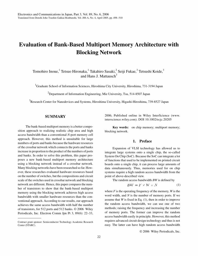
Figure 1 shows one implementation of the multiportmemory cell approach. The memory cell has multiple ports,so that all ports can access any memory cell without conflictunless the memory access address matches the addresswritten by the other processor. This approach can achievethe best performance, but the chip area increases in propor-tion to square of the number of ports, because all memorycells have multiple ports. For example, the chip area of a16-port SRAM implemented in a CMOS technology is 20times the chip area of a single-port SRAM [1].
2.2. Bank-based multiport memory
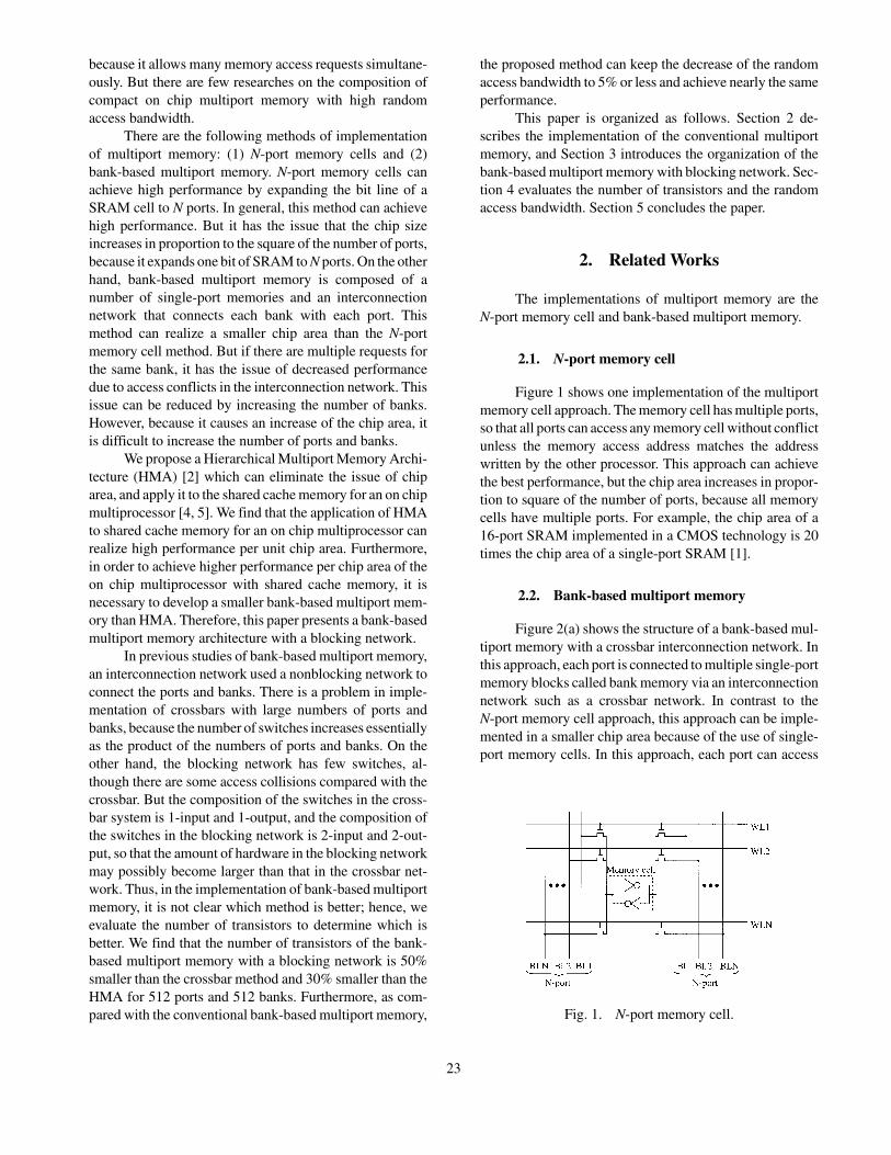
Figure 2(a) shows the structure of a bank-based mul-tiport memory with a crossbar interconnection network. Inthis approach, each port is connected to multiple single-portmemory blocks called bank memory via an interconnectionnetwork such as a crossbar network. In contrast to theN-port memory cell approach, this approach can be imple-mented in a smaller chip area because of the use of single-port memory cells. In this approach, each port can access
Fig. 1. N-port memory cell.
23
any memory bank. However, because this approach usessingle-port memory as bank memory, if two or more portsaccess one memory bank simultaneously, a bank conflictoccurs. To reduce bank conflict, it is effective to increasethe number of banks. But this causes an enlargement of chiparea because the transistors on the crosspoints in the cross-bar must be enlarged so as to drive highly loaded wires. Forthis reason, it is not easy to increase the number of banks.
In order to alleviate the problem, the HierarchicalMultiport Memory Architecture (HMA) has been intro-duced for the implementation of effective bank-based mul-tiport memory. Figure 2(b) shows the structure of the HMA.The HMA is similar to the bank-based multiport memoryusing a crossbar system, but it is devised for compactlayout. The HMA contains two unique circuits, namely, the1-to-N-port transition circuit on hierarchical level 1, and theconflict resolver on hierarchical level 2. The former per-forms 1-port to N-port or N-port to 1-port translation, andthe latter arbitrates port conflicts.
The HMA can be implemented in a smaller chip areabecause the hardware resources of the interconnection net-work are not proportional to the number of ports. Accordingto Ref. 2, the HMA approach can reduce chip area by 26%from that in the conventional bank-based multiport memoryif the number of ports is 8 and the number of banks is 8.
3. EBMA
In this section, we consider how the conventionalbank-based multiport memory uses the interconnection net-work, and we propose EBMA (EBSF-based Multiport
memory Architecture), which uses the EBSF (ExpandedBanyan Switching Fabrics) blocking network instead of thecrossbar system used in the conventional bank-based mul-tiport memory.
In contrast to the conventional bank-based multiportmemory using the crossbar system, EBMA has the follow-ing advantages.
(1) By using the blocking network, EBMA canachieve smaller chip area.
(2) EBMA does not need a large driver because thecrosspoint system which constructs the blocking networkdivides long metal wires with large capacitive loads.
In Fig. 2(a), the bank based multiport memory usingthe crossbar needs a large buffer between the crosspoint andthe bank memory to drive the long metal wires. However,if we adopt the blocking network, the long metal wires withlarge loads in the crossbar can be divided into several localwires, so that we can expect an increase in the operationfrequency.
3.1. The structure of EBMA
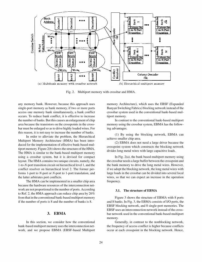
Figure 3 shows the structure of EBMA with 8 portsand 8 banks. In Fig. 3, the EBMA consists of I/O ports, theEBSF blocking network, and 8 single-port memories. TheEBSF uses an interconnection network instead of the cross-bar network used in the conventional bank-based multiportmemory.
Generally, in contrast to the nonblocking network,the frequency of access conflict is higher because conflictsoccur at each crosspoint in the blocking network. Hence,
Fig. 2. Multiport memory with crossbar and HMA.
24
this paper introduces the blocking network, which canreduce access conflicts, and allows the designer to defineits conflict ratio. Reference 7 proposes some blockingnetwork configurations based on a Banyan network withmultiple outlets per output in order to raise the accessbandwidth regardless of the use of a blocking network.Reference 7 proposes MBSF (Multi Banyan SwitchingFabrics), which uses K Banyan networks in parallel, EBSF,which expands its structure into K, TBSF (Tandem BanyanSwitching Fabrics), which connects K Banyan networks inseries, and PBSF (Piled Banyan Switching Fabrics), whichconnects K Banyan networks in a 3D structure. In order toreduce access conflicts in the blocking network, thoseblocking networks introduce a multiplex structure into theblocking network. We believe that the blocking networksdescribed in Ref. 7 can be introduced into the interconnec-tion network between ports and banks. Of the above net-works, we adopt EBSF because it can achieve low-accessconflicts with simple structure.
3.2. EBSF
EBSF is one of the blocking networks which canreduce access conflicts in the network because it expandsand multiplies the Banyan network. The EBSF consists ofMK/2 crosspoints per stage (vertical direction), and log2Mstages. The outlets of EBSF are K outlets useful at the last
stage. Here M is the number of banks and K is the numberof utilized Banyan networks. Hence, K equals the numberof input ports of the MUX in Fig. 3 divided by the numberof ports in EBMA. Furthermore, the number of ports inEBMA is the number of banks or less (N ≤ M). Figure 3shows the structure of EBSF in the case of 8 ports, 8 banks;the number of Banyan networks is doubled.
In bank-based multiport memory, to prevent accessconcentration at the same bank, the number of ports is setto the number of banks or less. In such cases, unusedcrosspoints at the first stages can be removed. For example,if the number of ports is reduced from 8 to 2 in Fig. 3, 6crosspoints in the first stage and 4 crosspoints in the secondstage can be removed.
To analyze the performance, the access rejectionprobability of the EBSF was estimated by a stochasticmodel in Ref. 7. According to Ref. 7, if N = 256 and K = 4,the access rejection probability of the EBSF is smaller byabout 40% than that of a normal blocking network, and thisis almost equal to the access rejection probability of thecrossbar network. In addition, the number of crosspoints inEBSF is theoretically smaller than that of the crossbarnetwork, since the EBSF consists of O(NM) crosspoints.On the other hand, the crossbar network hasO((MK / 2)log2M) crosspoints. But, because the size of thecrosspoint structures of EBSF and crossbar are different,we cannot easily estimate which is the smaller.
3.3. Circuit structures of EBMA
In this subsection, we describe the detailed circuitstructures of the EBMA as shown in Fig. 3.
3.3.1. The crosspoint structure of EBSF
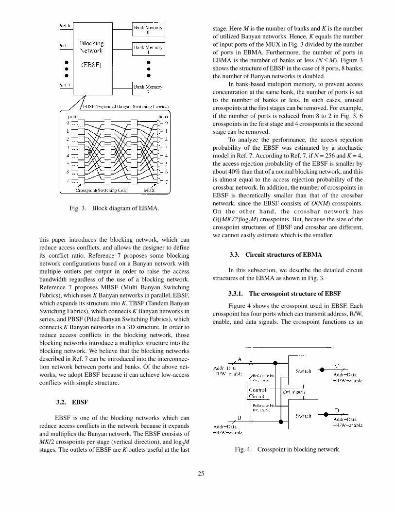
Figure 4 shows the crosspoint used in EBSF. Eachcrosspoint has four ports which can transmit address, R/W,enable, and data signals. The crosspoint functions as an
Fig. 3. Block diagram of EBMA.
Fig. 4. Crosspoint in blocking network.
25

exchange switch. To realize this function, the crosspointconsists of a control circuit and two switches. The twoswitches consist of an address switch and a data switch. Theaddress switch is a one-direction switch which transmitsmemory addresses from each port to one of the banks. Thedata switch is a bidirectional switch which transmits databetween each port and one of the banks.
1. Structure of the control circuit
Figure 5 shows the control circuit, which consists ofsimple combination logic implemented with 78 transis-tors.* To simplify the function of the control circuit, thepriority of the input ports is fixed. The control circuitgenerates the control signals (S0, S1, S2, S3) which controlthe CMOS switches for the address in Fig. 6 and the dataswitches in Fig. 7, and also the read/write control signals(R0, R1, W0, W1) which control the bidirectional tristateinverters in Fig. 7.
2. Structure of address switch
Figure 6 shows the circuit structure of the addressswitch, which uses exchange switches for the address sig-nals, R/W signals, and enable signals. The address switchconsists of four CMOS switches and two inverters used asoutput buffers. The four CMOS switches are controlled bythe signals (S0, S1, S2, S3) from the control circuit, andoutput exchanged signals from port A or port B to port C orport D via inverters. In case of exchange from port A to port
D, control signal S2 is active, so that the CMOS switchwhich connects between port A and port D is active. Theaddress switch consists of 12{log2(M1M2) + 3} transistors,where M1 is the total memory capacity and M2 is the numberof banks.
3. Structure of the data switch
Figure 7 shows the structure of the data switch whichexchanges data bidirectionally. The structure of the dataswitch is similar to the structure of the address switch, butit uses two tristate buffers instead of output buffers in theaddress switch. The four CMOS switches are controlled inthe same way by the signals (S0, S1, S2, S3) from thecontrol circuit. The bidirectional tristate inverters are con-trolled simultaneously by the signals (R0, W0, R1, W1)decoded by the control circuit. The data switch consists of24log2W transistors, where W is the bit width of a word.
*In this paper, the output signals of address switch and data switch areinverted signals from the input signals. Therefore, there are two kinds ofcontrol circuit with similar composition.
Fig. 5. Control circuit.
Fig. 6. Address switch.
Fig. 7. Data switch.
26
4. Evaluation
In this section, we present the evaluation results ofthe number of transistors and the access rejection prob-ability for the EBMA in comparison to the conventionalcrossbar memory.
As described above, we show the effectiveness of ourapproach in terms of the number of transistors to performmore precise evaluation. However, we cannot estimate theoperating frequency and the power consumption, becausethe performance of a chip layout, which is necessary toevaluate operation speed and power consumption of thecircuit, is time-consuming. Hence, this paper does notdiscuss the operating frequency and the power consumptionfurther.
4.1. Target
In this paper, we evaluate the following three ap-proaches.
Crossbar: a bank-based multiport memory using acrossbar system as the interconnection network in Section2.2.
HMA: a bank-based multiport memory based on theHMA technique described in Section 2.2.
EBMA: a bank-based multiport memory using anEBSF blocking network as the interconnection network asdescribed in Section 3.
4.2. Evaluation method
We present the results of evaluation of the number oftransistors and the access rejection probability.
4.2.1. Method of evaluation of the number oftransistors
The number of transistors of the EBMA was esti-mated based on the circuit structure in Section 3. Thenumber of transistors of the crossbar and HMA were esti-mated based on Refs. 3 and 8.
Incidentally, in order to compare the number of tran-sistors fairly, in each approach, it is necessary to equate theamount of the data which can be accessed in the memorysimultaneously. Thus, in this paper we impose the followingconditions: memory accesses occur from all ports simulta-neously, and the access time without conflict is the sameamong all ports.
4.2.2. Method of evaluation of access rejectionprobability
The access rejection probability was calculated by astochastic model. The access rejection probability is the
probability of bank conflicts and conflicts in the intercon-nection network during access.
1. Stochastic model of crossbar and HMA
If two or more ports access one bank simultaneously,crossbar and HMA access conflicts occur. We consider thefollowing five conditions.
1. The memory access probability from each port isthe same.
2. Memory accesses to every port occur in everycycle.
3. The destination of memory accesses is uniformlyspread over all banks.
4. If two or more ports access one bank simultane-ously, nonprioritized requests are blocked.
5. All memory accesses are synchronized.
In the case of N ports, M banks, and a probability p(n, N,M) that access to n arbitrary s ports will be successful, theaccess rejection probability of crossbar and HMA, namely,PCrossbar,HMA(N, M), was calculated by the following equa-tion:
Equation (2) indicates the access rejection probability ofthe ideal bank-based multiport memory. p(n, N, M) is rep-resented as follows:
where the first and second terms on the right-hand sidedenote the allowed combinations which are chosen in naccess requests from N ports. The third term represents allcombinations and the fourth term denotes n successfulaccesses in N ports.
2. Stochastic model of EBMA
In EBMA, there are two conflicts; access conflicts inthe same bank access, and conflicts at a crosspoint in theEBSF blocking network. The access rejection probabilityof EBMA, PEBMA(N, M, K), referred to in Refs. 7 and 10,was calculated using the output probability in the EBSFblocking network, Xn(xi) and PCrossbar,HMA(N, M).PEBMA(N, M, K) was represented as
(2)
(3)
(4)
27
where Xn(xi) denotes the probability of output to the next,(i + 1)-th, stage xi+1 ≡ Xn(xi) if there are access requests atstage i with a probabili ty of xi. Additionally,PEBMA(N, M, K) ≤ 1 and K ≥ 1. However, in Eq. (4), it isnecessary to take into consideration the efficiency of same-bank arbitration at the mux in EBSF. However, this isdifficult because there are two cases; the case of multipleaccess requests to the same bank, and the opposite case. Forthis reason, in Eq. (4), the arbitration efficiency at the muxin EBSF was calculated using the result of Eq. (3). Thus,the result of Eq. (4) represents a severe evaluation.
Next, to calculate Xn(xi) we analyzed the state of eachcrosspoint based on the following assumptions:
1. The memory access probability from each port ofthe EBMA is the same.
2. The destination of memory accesses is uniformlyspread over all banks.
3. In the crosspoint of EBSF, when output port re-quests from two input ports conflict, access priority isalways given to port A and the request from port B isrejected.
4. All memory accesses are synchronized.
If a memory access request occurs with probability x at theinput port of a crosspoint, the probability of request rejec-tion is 0.25x2 for a 2-input, 2-output crosspoint, and 0 for a1-input, 2-output crosspoint. Therefore, if a memory accessrequest occurs at the input port of a crosspoint in the i-thstage with probability xi, the probability for the next stagexi+1 ≡ Xn(xi) is represented as follows:
4.3. Evaluation results
4.3.1. Evaluation results of the number oftransistors
In this section, we present the ratios of the numbersof transistor used in each approach and the share of theinterconnection part in total memory.
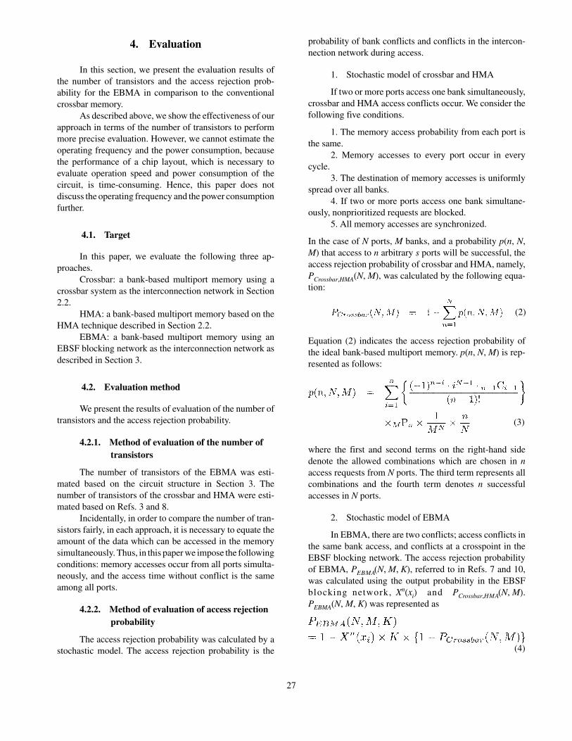
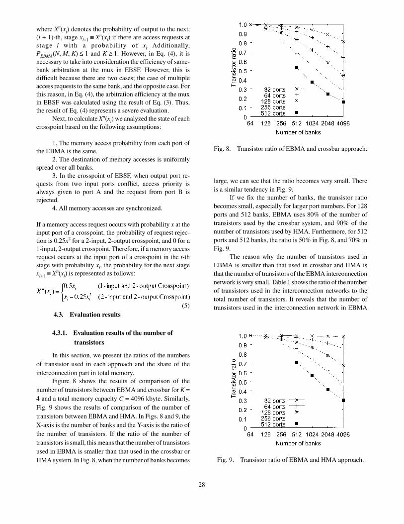
Figure 8 shows the results of comparison of thenumber of transistors between EBMA and crossbar for K =4 and a total memory capacity C = 4096 kbyte. Similarly,Fig. 9 shows the results of comparison of the number oftransistors between EBMA and HMA. In Figs. 8 and 9, theX-axis is the number of banks and the Y-axis is the ratio ofthe number of transistors. If the ratio of the number oftransistors is small, this means that the number of transistorsused in EBMA is smaller than that used in the crossbar orHMA system. In Fig. 8, when the number of banks becomes
large, we can see that the ratio becomes very small. Thereis a similar tendency in Fig. 9.
If we fix the number of banks, the transistor ratiobecomes small, especially for larger port numbers. For 128ports and 512 banks, EBMA uses 80% of the number oftransistors used by the crossbar system, and 90% of thenumber of transistors used by HMA. Furthermore, for 512ports and 512 banks, the ratio is 50% in Fig. 8, and 70% inFig. 9.
The reason why the number of transistors used inEBMA is smaller than that used in crossbar and HMA isthat the number of transistors of the EBMA interconnectionnetwork is very small. Table 1 shows the ratio of the numberof transistors used in the interconnection networks to thetotal number of transistors. It reveals that the number oftransistors used in the interconnection network in EBMA(5)
Fig. 8. Transistor ratio of EBMA and crossbar approach.
Fig. 9. Transistor ratio of EBMA and HMA approach.
28
is smaller than that in the crossbar and HMA systems. Theratio for EBMA is only 5% while those of the crossbar andHMA systems are 50 and 32%, respectively, for 512 portsand 512 banks. Hence, the number of transistors used in theinterconnection network in EBMA is much smaller than thenumber used in crossbar and HMA systems.
Next, we consider the reasons why the EBMA ap-proach can be implemented with fewer transistors than thecrossbar approach and the HMA approach. Before discuss-ing this reason, we subdivide circuit of each approach intothe following circuit elements, and estimate the total num-ber of transistors used in each circuit element.
Decoder: The bank decoder is the decoder circuit atthe crosspoints in crossbar systems, the row/column de-coder circuit on level 2 in HMA systems, and the controlcircuit at the crosspoints in EBMA.
Ctrl: the circuit used to control the data switch direc-tion in crossbar and HMA systems.
Addr sw: the address switch used to transmit addresssignals.
Data sw: the data switch used to transmit data signals.Bank buffer: I/O buffers in the bank memory of
crossbar systems and EBMA. In HMA, the circuit thatfunctions as I/O buffers in the 1-to-N-port transition circuit.
For example, we present the results for 4096 banksand K (the number of Banyans) = four. Figure 10 shows thenumber of transistors of each circuit in EBMA. Similarly,Fig. 11 shows that for a crossbar system and Fig. 12 showsthat for HMA. The X-axis is the number of ports and theY-axis is the number of transistors. In contrast to the cross-bar system in Fig. 11 and the HMA system in Fig. 12, theincrease in the number of transistors in EBMA is small. InFigs. 10 to 12, data switch constitutes a large part of thecircuit. Meanwhile, the ratios of the numbers of transistorsused in the data switch in crossbar and HMA systems areabout 70 to 80% of all memory, while the number oftransistors of the data switch in EBMA is about 60% of thetotal. Therefore, the difference in the number of transistorsis in the tens of percent. Figures 13 to 15 show the numberof transistors of each circuit other than the number oftransistors of the data switch. If we contrast EBMA withthe crossbar system, the number of transistors and theincrease in the number of transistors in EBMA is small,with the exception of 32 ports. Similarly, if we contrastEBMA with HMA, the number of transistors in EBMA islarger than in HMA for 32 to 128 ports, but the number oftransistors of EBMA is smaller than that in HMA for 256ports or more. Furthermore, the numbers of transistors used
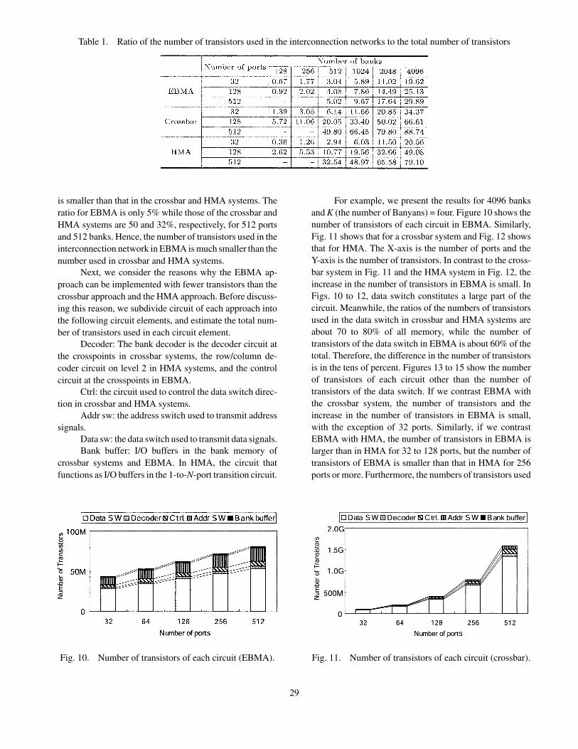
Table 1. Ratio of the number of transistors used in the interconnection networks to the total number of transistors
Fig. 10. Number of transistors of each circuit (EBMA). Fig. 11. Number of transistors of each circuit (crossbar).
29
for the decoder and ctrl in EBMA are smaller than those incrossbar and HMA systems. Hence, we infer that the rea-sons why the number of transistors in EBMA is smaller thanin crossbar and HMA systems are as follows: (1) The circuitstructure of the crosspoint in EBMA is simple. (2) Initially,the blocking network used in EBMA is constructed assum-ing that the number of ports is the same as the number ofbanks; afterward, in order to adjust the blocking networkstructure to a practical structure, we remove the unneces-sary parts. (3) Thus, the increase in the number of transistorsto the increase in the number of ports is small.
Thus, we can say the reason why the number oftransistors in the EBMA approach is smaller than in theother approaches is that the relation of the number oftransistors to the number of ports is constant.
4.3.2. Evaluation of access rejection probability
In this section, we show the access rejection prob-ability of each approach. Figure 16 shows the access rejec-tion probability of EBMA for 128 ports and 512 banks. TheX-axis is the number of Banyan networks and the Y-axis isthe access rejection probability. The dashed line shows theaccess rejection probability of crossbar and HMA systems.These are ideal results for bank-based multiport memory.If the number of Banyan networks used in EBSF is in-creased from 2 to 16, we can see that the access rejectionprobability of EBMA becomes small and is similar to thoseof the crossbar and HMA systems. In particular, if K, thenumber of Banyan networks, is 8 to 16, the difference inaccess rejection probability between EBMA and cross-bar/HMA is 10% or less. Figure 17 shows the accessrejection probability for 512 ports and 512 banks. In thiscase, the access rejection probabilities of all approaches are
Fig. 12. Number of transistors of each circuit (HMA).
Fig. 14. Number of transistors of each circuit withoutdata switch (crossbar).
Fig. 15. Number of transistors of each circuit withoutdata switch (HMA).
Fig. 13. Number of transistors of each circuit withoutdata switch (EBMA).
Fig. 16. Network size versus access rejectionprobability (128 ports, 512 banks).
30
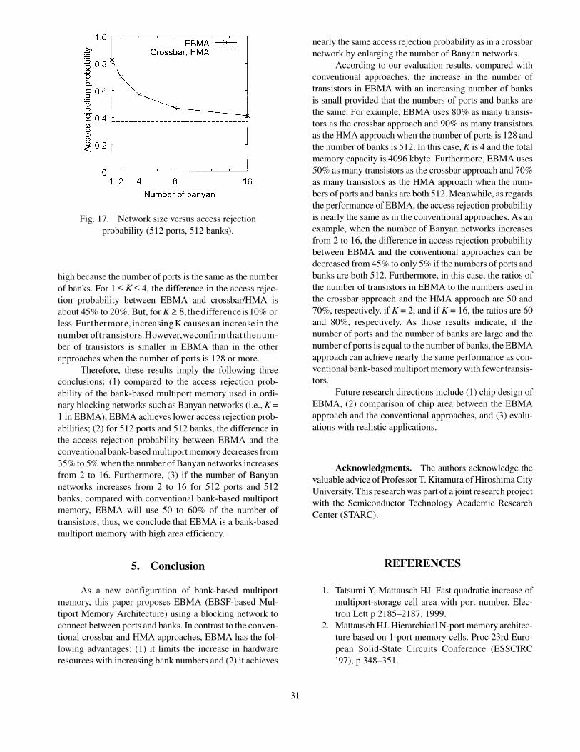
high because the number of ports is the same as the numberof banks. For 1 ≤ K ≤ 4, the difference in the access rejec-tion probability between EBMA and crossbar/HMA isabout 45% to 20%. But, for K ≥ 8, the difference is 10% orless. Fur thermore, increasing K causes an increase in thenumber of transistors. However, we confirm that the num-ber of transistors is smaller in EBMA than in the otherapproaches when the number of ports is 128 or more.
Therefore, these results imply the following threeconclusions: (1) compared to the access rejection prob-ability of the bank-based multiport memory used in ordi-nary blocking networks such as Banyan networks (i.e., K =1 in EBMA), EBMA achieves lower access rejection prob-abilities; (2) for 512 ports and 512 banks, the difference inthe access rejection probability between EBMA and theconventional bank-based multiport memory decreases from35% to 5% when the number of Banyan networks increasesfrom 2 to 16. Furthermore, (3) if the number of Banyannetworks increases from 2 to 16 for 512 ports and 512banks, compared with conventional bank-based multiportmemory, EBMA will use 50 to 60% of the number oftransistors; thus, we conclude that EBMA is a bank-basedmultiport memory with high area efficiency.
5. Conclusion
As a new configuration of bank-based multiportmemory, this paper proposes EBMA (EBSF-based Mul-tiport Memory Architecture) using a blocking network toconnect between ports and banks. In contrast to the conven-tional crossbar and HMA approaches, EBMA has the fol-lowing advantages: (1) it limits the increase in hardwareresources with increasing bank numbers and (2) it achieves
nearly the same access rejection probability as in a crossbarnetwork by enlarging the number of Banyan networks.
According to our evaluation results, compared withconventional approaches, the increase in the number oftransistors in EBMA with an increasing number of banksis small provided that the numbers of ports and banks arethe same. For example, EBMA uses 80% as many transis-tors as the crossbar approach and 90% as many transistorsas the HMA approach when the number of ports is 128 andthe number of banks is 512. In this case, K is 4 and the totalmemory capacity is 4096 kbyte. Furthermore, EBMA uses50% as many transistors as the crossbar approach and 70%as many transistors as the HMA approach when the num-bers of ports and banks are both 512. Meanwhile, as regardsthe performance of EBMA, the access rejection probabilityis nearly the same as in the conventional approaches. As anexample, when the number of Banyan networks increasesfrom 2 to 16, the difference in access rejection probabilitybetween EBMA and the conventional approaches can bedecreased from 45% to only 5% if the numbers of ports andbanks are both 512. Furthermore, in this case, the ratios ofthe number of transistors in EBMA to the numbers used inthe crossbar approach and the HMA approach are 50 and70%, respectively, if K = 2, and if K = 16, the ratios are 60and 80%, respectively. As those results indicate, if thenumber of ports and the number of banks are large and thenumber of ports is equal to the number of banks, the EBMAapproach can achieve nearly the same performance as con-ventional bank-based multiport memory with fewer transis-tors.
Future research directions include (1) chip design ofEBMA, (2) comparison of chip area between the EBMAapproach and the conventional approaches, and (3) evalu-ations with realistic applications.
Acknowledgments. The authors acknowledge thevaluable advice of Professor T. Kitamura of Hiroshima CityUniversity. This research was part of a joint research projectwith the Semiconductor Technology Academic ResearchCenter (STARC).
REFERENCES
1. Tatsumi Y, Mattausch HJ. Fast quadratic increase ofmultiport-storage cell area with port number. Elec-tron Lett p 2185–2187, 1999.
2. Mattausch HJ. Hierarchical N-port memory architec-ture based on 1-port memory cells. Proc 23rd Euro-pean Solid-State Circuits Conference (ESSCIRC’97), p 348–351.
Fig. 17. Network size versus access rejectionprobability (512 ports, 512 banks).
31
3. Fukae S, Omori N, Mattausch HJ, Koide T, Inoue T,Hironaka T. Comparison of the hierarchical andcrossbar-based architecture for the composition mul-tibank multiport memory. Tech Rep IEICE2002;CAS2002-48;37–42. (in Japanese)
4. Inoue T, Sasaki T, Hironaka T, Koide T, MattauschHJ. A study of compact and multi-banks memorysuitable for LSI. Tech Rep IEICE 2002;22:125–130.(in Japanese)
5. Sasaki T, Inoue T, Omori N, Hironaka T, MattauschHJ, Koide T. Chip size and performance evaluationsof shared cache for on-chip multiprocessor. J IEICE2004;J87-D-I:350–363. (in Japanese)
6. Tomita S. Parallel computer composition theory.ISBN: 4785630663, 1986. (in Japanese)
7. Hanawa T, Amano H. Performance analysis of MlNswith multiple outlets. J IPSJ 1995;36:1630–1639.
8. Fukae S, Omori N, Koide T, Mattausch HJ, Inoue T,Hironaka T. Optimized bank-based multi-portmemories through a hierarchical multi-bank struc-ture. Proc SASIMI2003, p 323–330.
9. Yamada K, Lee H, Murakami T, Mattausch HJ. Area-efficient circuit concept for dynamical conflict man-agement of N-port memories with multi-Gbit/saccess bandwidth. Proc 24th European Solid StateCircuits Conference (ESSCIRC’98), p 141.
10. Kumar M, Jump JR. Performance of unbuffered shuf-fle-exchange network. IEEE Trans Computer1986;35:573–578.
AUTHORS (from left to right)
Tomohiro Inoue received his M. S. degree in information engineering from Hiroshima City University in 2003 and iscurrently a doctoral student. His main interests include bank-based multiport memory architectures and their application tomultiprocessor architectures.
Tetsuo Hironaka received his B.E. degree from Yamaguchi University in 1988 and M.S. and Ph.D. degrees in engineeringfrom Kyushu University in 1990 and 1993. From 1993 to 1994, he was a research associate at Kyushu University. Since 1994,he has been an associate professor of computer systems at Hiroshima City University. His research interests are in the area ofreconfigurable architectures, system software, and on-chip multiprocessing. He is a member of IEICE, IPSJ, ACM, and IEEE.
Takahiro Sasaki received his B.S., M.S., and Ph.D. degrees in information engineering from Hiroshima City Universityin 1998, 2000, and 2003. His doctoral research was on efficient multiprocessor architecture. Since 2003 he has been on thefaculty of Mie University, where he is a research assistant in the Department of Information Engineering. His main interestsinclude multiprocessor architecture, low-power high-performance computing, and motion estimation LSI for MPEG. He is amember of IEICE and IPSJ.
Seiji Fukae received his B.S. degree from Kochi University in 1996 and M.S. and Ph.D. degrees in physics from HiroshimaUniversity in 1998 and 2001. Since 2001, he has been a research associate at the Research Center for Nanodevices and Systems,Hiroshima University. He is a member of the Physical Society of Japan.
32
AUTHORS (continued) (from left to right)
Tetsushi Koide received his B.E. degree in physical electronics and M.E. and Ph.D. degrees in systems engineering fromHiroshima University in 1990, 1992, and 1998. After serving as a research associate and an associate professor on the Facultyof Engineering at Hiroshima University and an associate professor at the VLSI Design and Education Center (VDEC) of theUniversity of Tokyo, he has been an associate professor at the Research Center for Nanodevices and Systems of HiroshimaUniversity since 2001. His research interests include system design and architecture issues for memory-based systems, real-timeimage processing, VLSI CAD/DA, genetic algorithms, and combinatorial optimization. He is a member of the Institute ofElectrical and Electronics Engineers, the Association for Computing Machinery, the Information Processing Society of Japan,and IEICE.
Hans J. Mattausch received his Dipl. Phys. degree from the University of Dortmund, Germany, in 1977 and Dr. rer. nat.degree from the University of Stuttgart, Germany, in 1981. He joined the Research Laboratories of Siemens AG, Munich, in1982, where he was involved in the development of MOS technology as well as the design of memory and telecommunicationcircuits. Beginning in 1990, he led a research group on MOS-technology-based power semiconductor devices, which includeddevice design, modeling and packaging. In 1995 he joined the Siemens Semiconductor Group as Manager of the Departmentfor Product Analysis and Improvement in the Chip Card IC Division. In 1996 he joined Hiroshima University, and is presentlya professor at the Research Center for Nanodevices and Systems. His main present interest is in system design and architectureissues for effective utilization of nanodevices and nanotechnology. He is a senior member of IEEE and a member of IEICE.
33