evaluation board user guide - analog devices€¦ · · 2017-02-15droop current sharing and...
TRANSCRIPT

Evaluation Board User Guide UG-566
One Technology Way • P.O. Box 9106 • Norwood, MA 02062-9106, U.S.A. • Tel: 781.329.4700 • Fax: 781.461.3113 • www.analog.com
240 W Evaluation Board Kit for the ADP1051, Digital Controller for Isolated Power
Supply with PMBus Interface
PLEASE SEE THE LAST PAGE FOR AN IMPORTANT WARNING AND LEGAL TERMS AND CONDITIONS. Rev. 0 | Page 1 of 40
FEATURES Full support evaluation kit for the ADP1051 240 W full bridge topology (adjustable to phase shifted full
bridge topology or half bridge topology) Input voltage range: 36 V dc to 75 V dc Output voltage: 12 V dc Nominal output current: 20 A Direct paralleling with multiple boards connected to a
common bus Synchronization as master device and slave device Droop current sharing and analog current sharing extension On-board tests for housekeeping functions LED indicated key status PMBusTM communication Graphical user interface (GUI) software
EVALUATION KIT CONTENTS ADP1051-240-EVALZ evaluation board ADP1051DC1-EVALZ daughter card CD with ADP1051 GUI installer, ADP1051 data sheet, UG-566
user guide, project sample files, schematics and BOMs for the ADP1051-240-EVALZ, ADP1051DC1-EVALZ, and current share daughter card
ADDITIONAL EQUIPMENT/SOFTWARE NEEDED ADP-I2C-USB-Z USB-to-I2C connector ADP-I2C-USB-Z drivers CD
GENERAL DESCRIPTION The ADP1051-240-EVALZ evaluation board, together with a ADP1051DC1-EVALZ daughter card, allows the user to evaluate the ADP1051 in a power supply unit (PSU) environ-ment. The boards are fully compatible with the ADP1051 GUI software. With the ADP-I2C-USB-Z USB-to-I2C connector and the GUI software, the ADP1051 on the evaluation board can be interfaced with a PC via a USB port.
The evaluation board allows the ADP1051 to be exercised without the need of external components. The board is set up to act as an isolated PSU, outputting a rated load of 12 V, 20 A from a 36 V dc to 75 V dc source.
Two parallel connectors on the evaluation board provide synchronization, share bus, and PMBus interfaces. They allow the direct paralleling evaluation when multiple evaluation boards are connected in parallel to a common bus. One analog current share daughter card connector allows analog current share extension.
Multiple test points allow easy access to all critical points/pins. Three LEDs give the user a direct visual indication of variations in the board status, such as the system input voltage, PGOOD output, and FLAGIN input.
Full performance details are provided in the ADP1051 data sheet, and the ADP1051 data sheet should be consulted in conjunction with this user guide.
EVALUATION BOARD SETUP
VIN+
VIN–
ADP-I2C-USB-Z
ADP1051DC1-EVALZ
VOUT+ADP1051-240-EVALZ
VOUT–
PC
1152
9-00
1
Figure 1. ADP1051 Evaluation Board Setup

UG-566 Evaluation Board User Guide
Rev. 0 | Page 2 of 40
TABLE OF CONTENTS Features .............................................................................................. 1 Evaluation Kit Contents ................................................................... 1 Additional Equipment/Software Needed ...................................... 1 General Description ......................................................................... 1 Evaluation Board Setup ................................................................... 1 Revision History ............................................................................... 2 Evaluation Board Hardware ............................................................ 3
Overview ........................................................................................ 3 Evaluation Board Characteristics ............................................... 5 Connectors .................................................................................... 5 Hardware Connection ................................................................. 6
Evaluation Board GUI Software ..................................................... 8 Overview ........................................................................................ 8 Downloading the GUI ................................................................. 8 Installing the GUI ......................................................................... 8 Launching the GUI ...................................................................... 8 Getting Started ............................................................................ 11 Project Sample Files ................................................................... 11
Evaluating the Board ...................................................................... 12 On/Off Control and Soft Start .................................................. 12 PWM Settings ............................................................................. 14
Digital Compensator and Load Transient Response ............. 14 Input Voltage Settings ................................................................ 16 Output Voltage Settings ............................................................. 17 Input Current Settings ............................................................... 19 Output Current Setting.............................................................. 19 Temperature Settings ................................................................. 22 Flags and Fault Response Configurations ............................... 22 Trimming ..................................................................................... 22 Synchronization .......................................................................... 23 Power Good Signal ..................................................................... 23 Phase Shifted Full Bridge Operation ....................................... 24 Direct Paralleling ........................................................................ 24
Additional Graphs .......................................................................... 26 Schematics and Artwork ............................................................... 27
ADP1051-240-EVALZ ............................................................... 27 ADP1051DC1-EVALZ .............................................................. 33 Current Share Daughter Card .................................................. 35
Ordering Information .................................................................... 37 Bill of Materials ........................................................................... 37
REVISION HISTORY 7/13—Revision 0: Initial Version

Evaluation Board User Guide UG-566
Rev. 0 | Page 3 of 40
EVALUATION BOARD HARDWARE OVERVIEW The ADP1051-240-EVALZ evaluation board and the ADP1051DC1-EVALZ daughter card feature the ADP1051 in a dc-to-dc switching power supply in full bridge topology with synchronous rectification. Figure 2 shows a hardware photo of the evaluation board. Figure 3 shows a block diagram of the main components on the board. The circuit is designed to provide a rated load of 12 V, 20 A from a dc input voltage source of 36 V dc to 75 V dc. The ADP1051 provides functions such as output voltage regulation, synchronization, constant current control, prebias start up, direct paralleling, and comprehensive protection.
The main transformer on the evaluation board breaks the dc-to-dc power supply into primary side and secondary side; therefore, creating isolation. On the primary side, the full bridge stage switches and inverts the dc voltage derived from the input terminals (J1 and J5) into ac voltage. The control signals for the full bridge stage come from the ADP1051 through the digital isolators (ADuM3210) and the half bridge drivers. There is also a current transformer (CT) sensing and transmitting the primary side current information to the ADP1051 on the secondary side.
On the secondary side, the full wave synchronous rectifiers (SR) rectify the ac voltage to dc voltage. An LC filter smooths the pulsated dc voltage. The current information is sensed through a current sense resistor and fed to the CS2+ and CS2− pins in the ADP1051. Output terminals, J2 and J6, are used for the load connection.
The ADP1051DC1-EVALZ daughter card shown in Figure 4 can be plugged into the daughter card connector (J8). It provides the signals that are used to regulate the output voltage, limit the output current, and control the on/off switch of the evaluation board. A 4-pin connector (J2) on the daughter card is used for I2C/PMBus communication through a USB-to-I2C connector, ADP-I2C-USB-Z. This allows the GUI software to communicate with the evaluation board through the USB port of the PC. If the J17 or J18 parallel connector is connected, the GUI can visit all the evaluation boards through a single USB-to-I2C connector. With this interface, users can monitor and program the ADP1051.
An auxiliary power supply on the evaluation board is used to generate a 10V_PRI bias power for full bridge drivers, a 5V_PRI bias power for the primary side power supply of the ADuM3210, and a 10V_SEC bias power for the ADP3654 driver. A 10V_VCC bias power is generated from an OR-diode network using a 10V_SEC bias power and 5 V voltage source from the USB-to-I2C connector. This allows the GUI access to the ADP1051 when the auxiliary power circuit is not powered up. The ADP3303 LDO converts 10V_VCC to a 3V3_SEC bias power for the ADP1051 and the secondary side power of the ADuM3210. Alternatively, the auxiliary power input can also come from an independent dc source through TP47 and TP50.
An analog current share connector (J15) allows an external current share daughter card to be used for analog current sharing control. Two parallel connectors (J17 and J18) allow the synchronization, current share, and PMBus communication between multiple evaluation boards.
There are wholly three blue color LEDs in the evaluation board to provide the status of the evaluation board. D7 indicates the input voltage signal. D17 indicates the PGOOD output (PG/ALT pin output signal). D18 indicates the FLAGIN signal.
There are three complete switches on the evaluation board. The SW1 switch is used to control the voltage level of the hardware CTRL pin. The SW2 and SW3 switches are used to change the part operating state between as master device and as slave device when the synchronization is enabled.
UG-566 Evaluation Board User Guide
Rev. 0 | Page 4 of 40
1152
9-00
2
Figure 2. ADP1051-240-EVALZ Evaluation Board
10V_PRINCP1031
VIN = 36V TO 75V
ADP3303
ON/OFF ANDUVP CONTROL
HIP 2101 HIP 2101
10V_SEC
AUXTRANSFORMER
ADP1051
CS2+CS2– OVP
VS+
VS–
AGND
SR1/SR2
I2CCONNECTOR
SDASCLRESADDRTDVDD
CTRL
OUTA/OUTB/OUTC/OUTD
CS1
SR FETs OUTPUT FILTER
VOUT (12V @ 20A)
ADP3654
ADuM3210
ADuM3210
ADuM3210
CT
MAINTRANSFORMER
FULL BRIDGE FETs
1152
9-00
3
Figure 3. Block Diagram of ADP1051-240-EVALZ Evaluation Board
1 152
9-00
4
Figure 4. ADP1051DC1-EVALZ Daughter Card

Evaluation Board User Guide UG-566
Rev. 0 | Page 5 of 40
EVALUATION BOARD CHARACTERISTICS
Table 1. Evaluation Board Characteristics Parameter Symbol Min Typ Max Unit Test Conditions/Comment INPUT VOLTAGE VIN 36 48 75 V dc OUTPUT VOLTAGE SETPOINT VOUT 12 V dc
VOUT OV Fault Limit (Default) 14 V dc Output Voltage Ripple 200 mV VIN = 48 V, VOUT = 12 V, IOUT = 20 A
OUTPUT CURRENT IOUT 0 20 A IOUT OC Fault Limit (Default) 25
OPERATION TEMPERATURE TA 25 50 °C Natural convection 25 85 °C Airflow = 200 LFM or above OT Fault Limit (Default) TOT_FAULT 110 °C
EFFICIENCY η 94.5 % VIN = 48 V, VOUT = 12 V, IOUT = 20 A SWITCHING FREQUENCY fSW 120 kHz DIMENSION
Width W 210 mm Length L 110 mm Component Height H 40 mm
CONNECTORS The connections to the ADP1051-240-EVALZ evaluation board are shown in Table 2. Table 3 to Table 6 show the details about these connectors.
Table 2. Evaluation Board Connections Connector Function J1 VIN+, dc input J5 VIN−, ground return for dc input J2 VOUT+, dc output J6 VOUT−, ground return for dc output J8 ADP1051 daughter card connector J15 Analog current share daughter card connector J17 Parallel Connector 1 J18 Parallel Connector 2
Daughter Card Connector J8
The connections to J8 are shown in Table 3.
Table 3. J8 Connections Pin Function 1 10V_VCC 2 VS− 3 VS+ 4 CS2− 5 CS2+ 6 VF 7 CS1 8 SR1 9 SR2 10 OUTA 11 OUTB 12 OUTC 13 OUTD 14 SCL 15 SDA 16 CTRL 17 PG/ALT
18 SYNI/FLGI 19 3V3_SEC 20 AGND 21 RTD 22 OVP

UG-566 Evaluation Board User Guide
Rev. 0 | Page 6 of 40
Analog Current Share Connector J15
The connections to J15 are shown in Table 4.
Table 4. J15 Connections Pin Function 1 CS2+ 2 CS2− 3 10V_SEC 4 3V3_SEC 5 IBUS 6 VF_ISHARE 7 AGND 8 AGND
Parallel Connector J17 and J18
The connections to J17 and J18 are shown in Table 5.
Table 5. J17 and J18 Connections Pin Function 1 SCL 2 SDA 3 SYNC 4 CTRL 5 AGND 6 10V_VCC 7 IBUS 8 AGND
Daughter Card I2C/PMBus Connector
The connections to J2 in the ADP1051 daughter card are shown in Table 6.
Table 6. J2 Connections Pin Function 1 5V 2 SCL 3 SDA 4 AGND
HARDWARE CONNECTION Caution
This evaluation board is supplied with high voltages and currents. Take extreme caution, especially on the primary side, to ensure safety for the user. It is strongly advised to switch off the evaluation board when not in use. A current-limit dc source is recommended to use as the input.
Required Equipment
• DC power supply capable of 36 V dc to 75 V dc, 10 A output
• Electronic load capable of 12 V, 25 A input • Oscilloscope capable of 500 MHz bandwidth or higher • PC with Microsoft Windows XP (32-bit), Vista (32-bit),
Windows 7 (32-bit), or Windows 8 (32-bit) • Precision digital multimeters (6-digit HP34401 or
equivalent) • Portable digital multimeters (fluke) for measuring up to
25 A dc current • ADP-I2C-USB-Z USB-to-I2C connector (see Figure 5)
available from Analog Devices, Inc.
1152
9-00
5
Figure 5. ADP-I2C-USB-Z USB-to-I2C Interface Connector

Evaluation Board User Guide UG-566
Rev. 0 | Page 7 of 40
Evaluation Board Configurations
There are a series of jumpers used for ADP1051-240-EVALZ hardware settings. All the jumper configurations have been completed during the evaluation board assembly. Table 7 shows the details of jumper configurations.
J3 and J4 are short pins for configuring the low-side output current sense method and high-side output current sense method. The low-side current sense method is used by default. T1 and T4 are current transformers for primary side current sense. Typically, T4 is used while T1 is not connected by default.
Users do not need to complete any hardware configuration unless special test items will be conducted.
Table 7. Jumpers Configuration Jumper Function JP1 Short this jumper to short the R46. This jumper can be
used as signal injection point during the control loop test. It is open by default.
JP2 Short this jumper to short R53. It is open by default. JP3 When SW1 is used to control the PSU, short this jumper.
It is shorted by default. JP4 When multiple evaluation boards are connected in
parallel, proper configuration of this jumper allows a single switch to control all evaluation boards. It is shorted by default.
JP5 Short this jumper to configure the on/off pin at an off state. It is open by default.
JP11 Short this jumper to select OUTD as a SYNO signal to J17 connector. It is open by default.
JP12 Short this jumper to select OUTC as a SYNO signal to J17 connector. It is open by default.
JP13 Short this jumper to select OUTD as a SYNO signal to J18 connector. It is open by default.
JP14 Short this jumper to select OUTC as a SYNO signal to J18 connector. It is open by default.
Connecting the Hardware
Do not connect the ADP-I2C-USB-Z connector to the evalua-tion board until after the GUI software has been installed.
Figure 6 shows the test configuration of the evaluation board. The digital multimeters are optional. An independent dc source can be applied on TP47 and TP50 to generate all bias power supplies even if the dc input is lower than 30 V. The board evaluation can start when the dc input voltage is increased from 0 V.
PC
J1
J5
DCPOWERSUPPLY
SW2SW1
ADP1051DC1-EVALZ
J8
J2
J6 –
+
–
+
ELECTRONICLOAD
5.40A
COMI
MULTIMETER
VICOM
48.00V
SW3
J17
J18ADP1051-240-EVALZ
J2 J15
20.00A
COMI
MULTIMETER
VICOM
12.00V
TP47
TP50
ADP-I2C-USB-Z
1152
9-00
6
JP4
Figure 6. Test Configuration for the Evaluation Board

UG-566 Evaluation Board User Guide
Rev. 0 | Page 8 of 40
EVALUATION BOARD GUI SOFTWARE OVERVIEW The ADP1051 GUI is a free software tool for programming and configuring the ADP1051. For more information on the GUI, refer to the ADP1051 GUI user guide.
DOWNLOADING THE GUI The ADP1051 GUI setup file is included on the CD in the ADP1051 evaluation kit.
Users can also visit http://www.analog.com/ADP1051 to obtain the latest version of GUI software.
INSTALLING THE GUI Warning
Do not connect the USB cable to the evaluation board until the software has been installed.
Installation Steps
To install the ADP1051 GUI software, use the following steps:
1. Insert the CD. 2. Double click ADP1051 Setup.msi installation file to start
the installation. 3. Click through the following windows (such as Figure 7). 4. In the Total Phase USB Setup window, click Next. 5. Check I accept the terms in the License Agreement after
reading it and click Next. 6. Check the Install USB drivers option when the driver is
not installed. If the driver has been installed, uncheck the Install USB drivers option. Then click Install.
7. After the installation, click Close to complete the driver installation.
8. When the Adobe Flash Player Installer window appears, check I have read and agree to the terms of the Flash Player License Agreement after reading it. Click INSTALL. If a newer version of Adobe Flash Player is already installed in the system, click Quit and continue.
9. Click Close to exit setup.
1152
9-00
7
Figure 7. GUI Installation
LAUNCHING THE GUI To launch the GUI, use the following steps:
1. Plug the ADP1051 daughter card into the J8 connector. 2. Ensure that the CTRL switch (SW1) is turned to the off
position. The off position is the left side by default. 3. Plug the ADP-I2C-USB-Z connector into the USB port
in the PC. 4. If the Found New Hardware - Total Phase Aardvark
I2C/SPI Host Adapter window appears, the PC automati-cally installs the hardware driver. Wait until the installation is finished. If this window does not appear, skip this step.
5. Connect the ADP-I2C-USB-Z connector to J2 on the ADP1051 daughter card.
6. Launch the ADP1051.exe file. The GUI software should report that the ADP1051 has been located on the board as shown in Figure 8.
7. Click Finish to proceed to the Monitor window (see Figure 10).
8. Click Unlock Chip Password (Button I in Figure 10) and enter the chip password in the following pop-up window. The default chip password is 0xFFFF. Click Enter after keying in the password to process the Setup tab as shown in Figure 11.
1152
9-00
8
Figure 8. Getting Started.

Evaluation Board User Guide UG-566
Rev. 0 | Page 9 of 40
If the user wants to load the default command and board settings file from a local folder, click Load Command and Board settings from a ‘.51s’ file to ADP1051 (Button A in Figure 11) and select the ADP1051-240W-EVALZ-Default.51s file when specifying the folder as shown in Figure 9. Because the ADP1051 in the evaluation kit is preprogrammed with the board and command settings, this step is optional.
1152
9-00
9
Figure 9. Load Board and Command Settings File

UG-566 Evaluation Board User Guide
Rev. 0 | Page 10 of 40
Table 8. shows a list of key buttons in the GUI. For more information about the ADP1051 GUI, refer to the ADP1051 GUI user guide.
Table 8. Key Buttons in the GUI Button Letter Button Description A
Load command and board settings from a ‘.51s’ file to the ADP1051 device.
B
Save command and board settings from the ADP1051 device to a ‘.51s’ file.
C
Generate a hex file of the command and board settings.
D
Access to the EEPROM.
E
Scan for the ADP1051 device.
F
Open a spy window to monitor I2C communication between the GUI and the ADP1051 device.
G
Program command and board settings into the EEPROM.
H
Unlock/lock the trim password.
I
Unlock/lock the chip password.
A
E F G H I
B C D
1152
9-01
0
Figure 10. Monitor Window in the GUI

Evaluation Board User Guide UG-566
Rev. 0 | Page 11 of 40
GETTING STARTED Connect a dc source (voltage range of 36 V dc to 75 V dc) at the J1 and J5 input terminals and connect an electronic load at the J2 and J6 output terminals. See Figure 6 for the correct configuration.
Connect the multimeters on the input terminals and output terminals separately as shown in Figure 6.
Connect the voltage probes at different test pins. Ensure that the differential probes are used and that the grounds of the probe are isolated if the measurements are made on the primary and secondary side of the transformer simultaneously.
Turn the CTRL switch (SW1) to the on position.
The evaluation board is now up and running, and ready for evaluation. The output should read 12 V dc.
After a successful startup, the PSU is in a steady state. The board’s LEDs provide the status of the board. D17 is turned on indicating that there are no faults detected. In case of a fault, the PGOOD LED will be turned off indicating that a flag has tripped. The Monitor tab in the GUI displays the appropriate state of the PSU.
After completing the programming of ADP1051, click Program command and board settings into EEPROM (Button G in Figure 11) to program the command and board settings into the EEPROM once the user wants to save the settings in the device.
Moreover, the user can use the Save Command and Board settings from ADP1051 to a ‘.51s’ file button (Button B in Figure 11) to generate a .51s file for the command and board settings.
Software Main Window
Figure 11 shows the main window. There are four tabs total in the main window: • Setup tab: All the setting windows are in this tab. It includes
the board settings and command setting windows. • Monitor tab: The readings and flags are monitored in this tab. • Commands Access tab: This tab provides the command
maps for direct access. • Password Settings tab: The PMBus command WRITE_
PROTECT and chip password can be configured in this tab.
PROJECT SAMPLE FILES There are a series of project sample files on the CD. Using the GUI software, the user can load the different project sample file from the CD to do different types of evaluation. The evaluation board hardware should be configured to half bridge topology if the half bridge sample settings are to be evaluated.
The default settings file is also stored as ADI_Default.51s in the GUI. After the GUI is stalled, the user can load the ADI_Default.51s file in the default folder to learn the default settings of the evaluation board.
Table 9. Project Sample Files File Name Description ADP1051-240-EVALZ-Default.51s ZVS full bridge converter sample file. This is the default settings file. ADP1051-240-EVALZ-HSFB-SAMPLE.51s Hard-switched full bridge converter sample file. ADP1051-240-EVALZ-FSFB-SAMPLE.51s Phase-shifted full bridge converter sample file. ADP1051-240-EVALZ-HB-SAMPLE.51s Half bridge sample file. ADP1051-240-EVALZ-OLFB-SAMPLE.51s Open-loop full bridge converter sample file. ADP1051-240-EVALZ-OLFF-SAMPLE.51s Open-loop input voltage feed forward converter sample file.
A
E F G H I
B C D
1 152
9-0 1
1
Figure 11. Main Setup Window of the ADP1051 GUI (See Also Table 8)

UG-566 Evaluation Board User Guide
Rev. 0 | Page 12 of 40
EVALUATING THE BOARD This ADP1051 evaluation kit allows the user to get an insight into the flexibility offered by the extensive ADP1051 program-ming options. The following sections provide an overview of evaluation items to evaluate the key features of the ADP1051. Unless otherwise specified, use the project sample file ADP1051-240-EVALZ-Default.51s (it is preprogrammed in the ADP1051 of the daughter card) to do all the evaluation.
ON/OFF CONTROL AND SOFT START This section specifies the power-on control behavior, power- off control behavior, and the soft start timing of the PSU. By default, the AND logic of the hardware CTRL pin logic and software OPERATION command are used to turn on the ADP1051, as shown in the CTRL Settings window of the Setup tab (Figure 12). It is recommended that Switch SW1 be used to control the operation state of the PSU.
The turn-on delay time, turn-on rise time, and the turn-off delay time can be programmed in Soft Start and Stop window of the Setup tab (see Figure 13). Additional soft start settings are programmed in Figure 14. Figure 15 and Figure 16 show the results of soft start at 0 A load and 20 A load separately. The soft start rise time is programmed to 40 ms. Figure 17 gives an example of soft start with disabled synchronous rectifiers during soft start ramp.
1152
9-01
2
Figure 12. CTRL Settings Window
1152
9-01
3
Figure 13. Soft Start and Stop Settings Window
1152
9-01
4
Figure 14. Additional Soft Start Settings Window
1 152
9-01
5
Figure 15. Soft Start at 48 V DC Input, 0 A Load
1152
9-01
6
Figure 16. Soft Start at 48 V DC Input, 20 A Load
1152
9-01
7
Figure 17. Soft Start with Disabled SRs

Evaluation Board User Guide UG-566
Rev. 0 | Page 13 of 40
Prebias Start Up
The prebias start-up function provides the capability to start up with a prebiased voltage on the output. To set up the prebias startup, use the following steps:
1. Enable the prebias start up and program the appropriate nominal modulation value for prebias startup through the additional soft start settings window shown in Figure 14.
2. Select the type of prebias start up as shown in Figure 18:
• If the closed-loop input voltage feed forward operation is enabled and the input voltage information is available for the ADP1051 before the PSU starts up, select the Feed Forward always Activated option (Option A).
• If the closed-loop input voltage feedforward operation is disabled and the input voltage information is availa-ble for the ADP1051 before the PSU starts up, select the Feed Forward only during Startup option (Option B).
• If the closed-loop feed forward operation is disabled and the input voltage information is not aviable for ADP1051 before the PSU starts up, select the Feed Forward always Disabled option (Option C).
1152
9-01
8
A
B
C
Figure 18. Feed Forward Selection Option
Figure 19 and Figure 20 show the prebias start up waveforms when the Feed Forward always Activated option (Option A) is selected.
1152
9-01
9
Figure 19. Prebias Start Up at 36 V DC Input and Low Residual Voltage
1152
9-02
0
Figure 20. Prebias Start Up at 60 V DC Input and High Residual Voltage
Because the input voltage cannot be sensed through the wind-ings of auxiliary power supply in this evaluation board, it is recommended that the Feed Forward always Disabled option (Option C) be selected for evaluation.
Other evaluation options are:
• Program different turn-on rise time in combination with different turn-on delay time.
• Blank different flags during soft start ramp as shown in Figure 14.
• Choose different soft start gains to derive a best soft start ramp.
• Enable the SR soft start and select a different SR soft start speed to prevent a glitch at the output voltage ramp.

UG-566 Evaluation Board User Guide
Rev. 0 | Page 14 of 40
PWM SETTINGS The PWM timings for the primary side switches and secondary side synchronous rectifiers are programmed in the PWM SR Settings window of the Setup tab as shown in Figure 21. This window allows the programming of the switching frequency, rising edge and falling edge timings, the type of modulating edge (rising edge or falling edge), modulation type (positive or negative), and modulation limit. Figure 21 shows the gate drive signals at the output pins of the ADP1051. The QA, QB, QC, QD, Q7/Q8, and Q3/Q4 switches in the evaluation board ADP1051-240-EVALZ are driven separately by PWM outputs OUTA, OUTB, OUTC, OUTD, SR1, and SR2.
Although the switching frequency can be adjusted, the GUI software does not account for the dead times and the PWM timings have to be programmed manually to guarantee the normal operation of the PWM outputs.
1152
9-02
1
Figure 21. PWM SR Settings Window
Additional PWM and SR evaluation options are:
Enable and disable the pulse skipping mode and measure the standby power of the PSU.
Double the switching frequency from 120 kHz to 240 kHz. The board is designed to operate at a switching frequency of up to 240 kHz with airflow cooling.
Program an imbalance in the on time of the QA and QC switches, and evaluate the volt-second balance control function.
Run the software in simulation mode and program the PWM settings for different topologies such as zero-voltage-switched full bridge, hard-switched full bridge, phase shifted full bridge, half bridge, push-pull, two-switch forward, or active clamp forward converters. The project sample files listed in Project Sample Files section can also be loaded.
Align all SR edges to OUTA, OUTB, OUTC, OUTD edges and adjust the primary-secondary propagation delay by programming the SR1 and SR2 delay.
Program the adaptive dead time compensation function as shown in Figure 22 to improve the efficiency at light load condition.
1152
9-02
2
Figure 22. Adaptive Dead Time Compensation Settings Window
DIGITAL COMPENSATOR AND LOAD TRANSIENT RESPONSE The digital compensator can be configured by the Filter Settings window of the Setup tab as shown in Figure 23. The digital compensator can be changed by manipulating the position of the poles and zeros in the s-domain. The ADP1051 allows two different sets of compensator responses to be programmed. One is normal mode compensator and the other is light load mode compensator.
The digital compensator is a Type III compensator. The first pole is placed at a dc position to eliminate the steady state error. The second pole can be freely placed (ideally at the ESR zero position). However, the third pole is fixed at half of the switching frequency.
1152
9-02
3
Figure 23. Filter Settings Window
Warning
While varying the compensator's parameters is possible when the part is running, the wrong combination of parameters can cause the system to become unstable.
Evaluation Board User Guide UG-566
Rev. 0 | Page 15 of 40
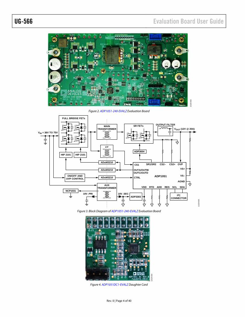
Control Loop Configuration
To configure the control loop, use the following steps:
1. Make sure the board parameters are set correctly, including the topology, the turn ratio of the main transformer, the output LC filter parameters, and the output voltage sense network parameters. Using the information, the GUI software generates the Bode plots of the power stage and output voltage sense network separately.
2. The switching frequency is determined in the PWM SR Settings window. Changing of the switching frequency changes the low frequency gain and the third pole position.
3. The user can start to place the zeros and poles, and set the low frequency gain and high frequency gain of the digital compensator, based on the stability rules.
4. The GUI then displays the full loop gain crossover frequency, the phase margin, the gain margin, and the phase crossover frequency.
5. Using the loop analyzer, the user can verify the pro-grammed control loop as shown in Figure 24. During the test on the control loop, the test signal from the loop analyzer can be easily injected in JP1 of the evaluation board.
100
40
32
16
24
8
–8
–24
0
–16
–32
–40
200
160
80
120
40
–40
–120
0
–80
–160
–2001k 10k
FREQUENCY (Hz)
MA
GN
ITU
DE
(B ÷
A) (
dB)
PHA
SE (B
–A
) (D
egre
es)
100k
1152
9-02
4
PHASE
MAGNITUDE
Figure 24. Control Loop Test by AP300 Loop Analyzer
Transient Response for the Load Step
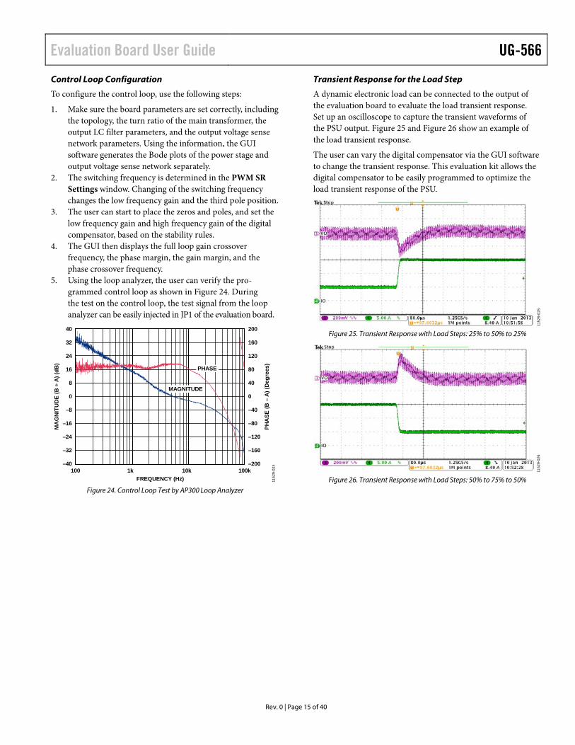
A dynamic electronic load can be connected to the output of the evaluation board to evaluate the load transient response. Set up an oscilloscope to capture the transient waveforms of the PSU output. Figure 25 and Figure 26 show an example of the load transient response.
The user can vary the digital compensator via the GUI software to change the transient response. This evaluation kit allows the digital compensator to be easily programmed to optimize the load transient response of the PSU.
1152
9-02
5
Figure 25. Transient Response with Load Steps: 25% to 50% to 25%
1152
9-02
6
Figure 26. Transient Response with Load Steps: 50% to 75% to 50%

UG-566 Evaluation Board User Guide
Rev. 0 | Page 16 of 40
INPUT VOLTAGE SETTINGS If the input voltage can be sensed by ADP1051 before the PSU is turned on (for example, the input voltage is sensed through the transformer windings of the auxiliary power circuit), the VIN on and VIN off limits can be programmed to control the input UVLO protection. Using the VIN Settings window in the Setup tab as shown in Figure 27, the user can program the VIN On limit and VIN Off limit.
By proper selection of the input voltage feed forward options as shown in Figure 18, the input voltage feed forward can be evaluated in different ways. Figure 28 gives a result of the input voltage transient with the feed forward being disabled (Option C—Feed Forward always Disabled in Figure 18). While Figure 29 gives a result of the input voltage transient with the input voltage feed forward being enabled (Option A—Feed Forward always Activated in Figure 18).
Additional input voltage related evaluation options are:
• Apply a different input voltage compensation multiplier (Register 0xFE59) to get an accurate input voltage sense at both no load and heavy load conditions.
• Select the input voltage signal to trigger the VIN_LOW flag or the VIN_UV_FAULT flag in the feed forward selection window shown in Figure 18.
1152
9-02
7
Figure 27. VIN Settings Window
1152
9-02
8
Figure 28. Input Voltage Transient Response with Feed Forward Disabled
1152
9-02
9
Figure 29. Input Voltage Transient Response with Feed Forward Enabled

Evaluation Board User Guide UG-566
Rev. 0 | Page 17 of 40
OUTPUT VOLTAGE SETTINGS The VOUT Settings windows (shown in Figure 30 and Figure 31) set all the output voltage related parameters, such as the output voltage settings, the droop resistor (through the VOUT_DROOP command), the output voltage transition rate (through the VOUT_TRANSITION_RATE), and conditional overvoltage protection setting. Figure 32 and Figure 33 provide results of output voltage adjustment when the VOUT transition rate is programmed as 3.125 µV/µs.
1152
9-03
0
Figure 30. VOUT Settings Window 1
1152
9-03
1
Figure 31. VOUT Settings Window 2
11
529-
032
Figure 32. VOUT Adjusted from 10 V to 12.5 V with 3.125 µV/µs Transition Rate
1152
9-03
3
Figure 33. VOUT Adjusted from 12.5 V to 10 V with 3.125 µV/µs Transition Rate

UG-566 Evaluation Board User Guide
Rev. 0 | Page 18 of 40
Droop Current Sharing
This test can be conducted by plotting the V-I curve when the load current is gradually increased from 0 A to 20 A. It can also be conducted by applying a dynamic load to test the transient performance. Moreover, the drooping current share test can be conducted using two or more evaluation boards connected in parallel. The settings of drooping current sharing are shown in Figure 31. The droop resister is programmed as 20 mΩ and the IOUT update rate is programmed as 82 µs. Figure 34 gives drooping current sharing accuracy using two ADP1051-240-EVALZ evaluation boards connected in parallel.
0
20
16
12
8
4
0
–46 12 18
LOAD CURRENT (A)
PSU
OU
TPU
T C
UR
REN
T (A
)
24 30 36
1152
9-03
4
BOARD A
BOARD B
Figure 34. Droop Current Sharing Accuracy
Output Overvoltage Protection
This test can be conducted in a number of ways. The simplest way is to set the output voltage to a value higher than the VOUT OV fault limit shown in Figure 30. Alternatively, shorting of the VS+ pin to AGND in the ADP1051 daughter card can cause a fast output overvoltage condition. The responses of the fault conditions can be programmed in the Flags and Fault Response Configurations section (see Figure 48). Figure 35 shows the waveforms when the response to an output overvoltage condition occurred.
The ADP1051 also supports the conditional overvoltage protection. The settings of conditional output overvoltage protection are shown in Figure 31. Figure 36 shows a result of conditional overvoltage protection when the outputs of two evaluation boards are connected to a common bus.
1152
9-03
5
Figure 35. Overvoltage Protection Waveform
1152
9-03
6
Figure 36. Conditional Overvoltage Protection with Two Evaluation Boards
Connected to a Common Bus
Output Undervoltage Protection
This test can be done in a number of ways. The simplest way is to set the output voltage to a value lower than the VOUT UV fault limit value shown in Figure 30. Even a shorted load or an internal short (such as shorting of the synchronous rectifiers) can cause an output undervoltage condition. The response of the fault condition can be programmed in the Flags and Fault Response Configurations section.

Evaluation Board User Guide UG-566
Rev. 0 | Page 19 of 40
INPUT CURRENT SETTINGS The input current settings are accessed using the CS1 and CS3 Settings window as shown in Figure 37. This window is used to program the cycle-by-cycle current limiting, the input over-current fast fault protection, the CS3 overcurrent protection and the volt-second balance control.
1152
9-03
7
Figure 37. CS1 and CS3 Settings Window
CS1 Cycle-by-Cycle Current Limiting
The leading edge blanking time, the leading edge blanking reference, debounce time, the PWM disabling selection, and the matched cycle-by-cycle current limiting can be pro-grammed in CS1 Settings window shown in Figure 37.
Input Overcurrent Fast Fault Protection
This test can be conducted by shorting the load. Using the setting window shown in Figure 37, the user can specify the IIN OC fast fault limit value by 2, 8, 16, 64, 128, 256, 512, or 1024. The fault response can be configured in the Flags and Fault Response Configurations section.
OUTPUT CURRENT SETTING The output current settings window is accessed using the IOUT Settings window. This window features the output overcurrent fault limit, the thresholds for the light load threshold and the deep light load, the responses for the light load threshold and the deep light load, the constant current mode, and the SR reverse current control.
1152
9-03
8
Figure 38. IOUT Settings Window 1
1152
9-03
9
Figure 39. IOUT Settings Window 2

UG-566 Evaluation Board User Guide
Rev. 0 | Page 20 of 40
Output Overcurrent Protection
This test can be conducted by applying a load current larger than the value programmed by the IOUT OC fault limit (shown in Figure 38). The fault response is programmed in the Fault Response window shown in Figure 48.
Figure 40 gives an experimental result by setting the IOUT OC fault limit at 25 A and enabling soft start after every 250 ms.
1152
9-04
0
Figure 40. IOUT OC Response Experimental Result
Constant Current Mode
Prior to the constant current mode test, the user needs to configure the constant current mode settings in Figure 39, including the output voltage change rates and the output current averaging speeds.
This test can be conducted in multiple ways:
• The constant current mode happens during a soft start at a CR load. The test is done on a standalone evaluation board.
• The constant current mode happens during a soft start at a CV load. The test is done on a standalone evaluation board.
• The constant current mode happens during a CR load transient. The test is done on a standalone evaluation board.
• The constant current mode happens during a CV load transient. The test is done on a standalone evaluation board.
• The constant current mode happens during a soft start when two or more evaluation board are connected in parallel. The load is a CR load.
• The constant current mode happens during a soft start when two or more evaluation boards are connected in parallel. The load is a CC load.
Figure 41 shows a result that the constant current mode happens during a soft start at a CR load. The test is done on a standalone evaluation board.
Figure 42 and Figure 43 show results that the constant current mode happens during a soft start when two evaluation boards are connected in parallel. The load is a CR load.
1152
9-04
1
Figure 41. Constant Current Control During Startup; Constant Current
Threshold is 10 A
1152
9-04
2
Figure 42. Constant Current Control with Two Evaluation Boards in Parallel;
Turn-On Timing is the Same
1152
9-04
3
Figure 43. Constant Current Control with Two Evaluation Boards in Parallel;
Turn-On Timing Difference is 50 ms

Evaluation Board User Guide UG-566
Rev. 0 | Page 21 of 40
SR Reverse Current Protection
This test can be conducted by several ways:
• At a no load condition, the VOUT voltage is adjusted from a higher voltage to a lower voltage with the fastest VOUT
transition rate. Up to 10,000 µF capacitance is connected at output terminals.
• Switch the load current between full load and no load with the fastest current slew rate programmed by E-load.
• At a no load condition, use an air switch to short the input terminals. A capacitor with up to 10,000 µF capacitance can be connected at the output terminals. This is a typical input voltage dip test.
Figure 44 shows a result where the output voltage is adjusted from a higher voltage to a lower voltage. Figure 45 shows a result that the input is shorted by an air switch.
1152
9-04
4
Figure 44. SR Reverse Current Protection During Output Voltage Adjustment
1 152
9-04
5
Figure 45. SR Reverse Current Protection During Input Dip Test; 10,000 µF
Capacitance is Connected at Output Terminal
Light Load Efficiency Optimization
The ADP1051 can be programmed to optimize performance when the output current drops below a certain level. The light load mode threshold and deep light load mode threshold are programmed in a manner to reduce the losses and increase the efficiency. A hysteresis for the light load mode and the deep light load mode is provided on the thresholds to avoid the current oscillations. The thresholds for light load mode and deep light load mode can also be programmed in the IOUT window as shown in Figure 39.
When operating in the light load mode or deep light load mode, the mode flag is set in the Monitor tab. In combination with the pulse skipping mode, the standby power consumption can be reduced.
The user can try the test items as follows:
• Try different thresholds for light load mode and deep light load mode to test the efficiency improvement.
• Try different averaging speed for light load mode and deep light load mode to test the transient response by applying a dynamic load.
• Program the threshold for the pulse skipping mode to test the efficiency improvement during standby mode.
• Select the PWM channels to be disabled during the deep light load mode as shown in Figure 46.
1152
9-04
6
Figure 46. Deep Light Load Response Check Box

UG-566 Evaluation Board User Guide
Rev. 0 | Page 22 of 40
TEMPERATURE SETTINGS This test can be conducted by enclosing the evaluation board in a thermal chamber at the desired ambient temperature to simulate the operating condition. The user can program the OT fault limit and OT warning limit through the Temperature Settings window shown in Figure 47. The OT hysteresis is the value difference of OT fault limit and OT warning limit.
1152
9-04
7
Figure 47. Temperature Settings Window
FLAGS AND FAULT RESPONSE CONFIGURATIONS The fault responses can be programmed in the Fault Response window of the Setup tab as shown in Figure 48. The state of faults can be monitored in the Monitor tab as shown in Figure 11. There are two groups of fault responses:
• PMBus faults responses, including IOUT OC, VOUT OV, VOUT UV, and OT.
• Manufacturer specific fault responses, including IIN OC FAST, CS3 OC, VIN UV, Flagin, SR RC, VDD OV. There is a global reenabling timing for all manufacturer specific fault responses.
The user can test this section by applying a fault condition. By changing the settings of the debounce timing, delay timings, responses and reenable timings, the user can see different protection performance.
When there is a fault causing the power supply to be shut down and a soft start is required if the PWM outputs are reenabled, the first fault ID information is shown in the Monitor tab. The first flag ID register gives the user more information for fault diagnosis than a simple flag.
1152
9-04
8
Figure 48. Fault Response Window
TRIMMING This test allows the entire power supply to be calibrated and trimmed digitally through the ADP1051 in the production environment.
All the ADP1051 parts are factory calibrated. The trimming is not needed if the voltage and current sense resistors have a high enough accuracy (see the ADP1051 data sheet for details). However, the ADP1051 can be retrimmed by the user to com-pensate for the errors introduced by external components. All the trimming can be done in the Trim Settings window of the Setup tab as shown in Figure 49.
1 152
9-04
9
Figure 49. Trimming Window

Evaluation Board User Guide UG-566
Rev. 0 | Page 23 of 40
SYNCHRONIZATION Synchronization as a Master Device
This test can be done by specifying OUTC or OUTD as a SYNO signal using the Sync Settings window of the Setup tab as shown in Figure 50. The SYNO signal should be stable to constantly represent the internal switching frequency once the ADP1051 VDD voltage is applied.
Jumper JP11 to Jumper JP13 can be used to configure OUTC or OUTD connected to SYNO. The user can test the SYNO clock through the test point TP35 or the SYNC pin in the JP17 and JP18 connectors.
Synchronization as a Slave Device
This test can be done by applying an external clock signal in the TP25 test point. Alternatively, the external clock signal (such as SYNO signal in the master device) can be applied in the SYNC pin of the J17 or J18 connector.
The settings can be programmed in the Sync Settings window (see Figure 50). To view the synchronization performance, try the following items:
• Enable and disable synchronization. • Set different delays to see the phase shift between master
device and slave device. • Program the different phase capture range. • If the external clock signal is generated by a signal
generator, the user can try to program the clock signal in sweep mode or burst mode to see the synchronization locking or unlocking.
1152
9-05
0
Figure 50. Synchronization Configurations
POWER GOOD SIGNAL This test can be conducted by applying a fault condition, which is used to trigger a PGOOD flag and pull down the PG/ALT pin. The user can follow the PGOOD Settings window shown in Figure 51 to program which fault signal asserts the PGOOD flag. In the case of a fault to trigger the PGOOD flag, the D17 LED is turned off indicating that the power supply is not good. Figure 52 shows that a VOUT_UV_FAULT flag triggers the PGOOD output (PG/ALT pin).
1152
9-05
1
Figure 51. PGOOD Configurations
1152
9-05
2
Figure 52. A VOUT_UV_FAULT Flag to Trigger PGOOD

UG-566 Evaluation Board User Guide
Rev. 0 | Page 24 of 40
PHASE SHIFTED FULL BRIDGE OPERATION The PWM settings for phase shifted full bridge operation is highly flexible. Either the QA/QB leg (controlled by OUTA/ OUTB PWM outputs) or the QC/QD leg (controlled by OUTC/ OUTD PWM outputs) can be configured to run in modulation mode. Figure 53 provides a PWM setting example of the QA/QB leg in positive modulation mode. In this case, the QA/QB leg is the leading leg and the QC/QD leg is the lagging leg.
All the test items are similar to the general full bridge operation. The only difference is the SR reverse current protection. In case of SR reverse current, configure the synchronous rectifier to be disabled. The user can load the phase shifted full bridge project sample file, ADP1051-240-EVALZ-FSFB-SAMPLE.51s, to do the evaluation.
1152
9-05
3
Figure 53. Phase Shifted Full Bridge PWM Setting Window
1152
9-05
4
Figure 54. PWM Waveforms under PSFB Operation
DIRECT PARALLELING The direct paralleling function is that multiple power supplies output rails are connected directly to a common bus without the existing of OR’ing devices. To overcome the challenges for direct paralleling, implement the following series of features:
• Prebias start up. • Current sharing. Use drooping current sharing or active
current sharing (through the current share daughter card). • Synchronous rectifiers reverse current protection to avoid
sinking current in a power supply. • Constant current control and hot-switching control. • Synchronization to reduce the output voltage ripple. • Conditional overvoltage protection for redundant control.
All the previous features are implemented in the ADP1051-240-EVALZ evaluation board.

Evaluation Board User Guide UG-566
Rev. 0 | Page 25 of 40
Figure 56 shows the setup of two ADP1051-240-EVALZ evaluation boards connected in parallel for direct paralleling test. Each board can be controlled by SW1 on each board (R73 should be removed). Alternatively, the SW1 on Board B can be configured to control both Board A and Board B. In this case, remove the JP4 jumper on Board A. For synchronization, if the ADP1051 in Board A is assigned as a slave device, then assign the ADP1051 in Board B as a master device. In this case, the SW2 in Board A should be turned to the slave position and the SW3 in Board B should be turned to the master position.
All the features listed in this section can be conducted in this direct paralleling system.
1152
9-05
6
Figure 55. Parallel Cable to Connect Two Evaluation Boards
PC
BOARD A
BOARD B
J1
J5
DCPOWERSUPPLY
SW2SW1
ADP1051DC1-EVALZ
J8
J2
J6
–
+
SW3
J17
J18ADP1051-240-EVALZ
J2
J1
J5
SW2SW1
ADP1051DC1-EVALZ
J8
J2
J6
SW3
J17
J18ADP1051-240-EVALZ
J2
ADP-I2C-USB-Z
1152
9-05
5
JP4
JP4
ELECTRONICLOAD
–
+
Figure 56. Direct Paralleling Configuration when Two Evaluation Boards are Connected in Parallel
UG-566 Evaluation Board User Guide
Rev. 0 | Page 26 of 40
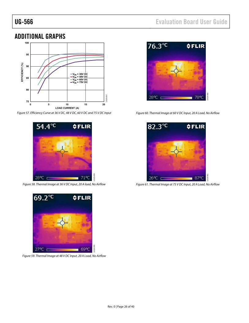
ADDITIONAL GRAPHS
0
100
95
90
85
80
755 10 15
LOAD CURRENT (A)
EF
FIC
IEN
CY
(%
)
2011
529-
057
VIN = 36V DCVIN = 48V DCVIN = 60V DCVIN = 75V DC
Figure 57. Efficiency Curve at 36 V DC, 48 V DC, 60 V DC and 75 V DC Input
1152
9-05
8
Figure 58. Thermal Image at 36 V DC Input, 20 A load, No Airflow
1152
9-05
9
Figure 59. Thermal Image at 48 V DC Input, 20 A Load, No Airflow
1152
9-06
0
Figure 60. Thermal Image at 60 V DC Input, 20 A Load, No Airflow
1152
9-06
1
Figure 61. Thermal Image at 75 V DC Input, 20 A Load, No Airflow

Evaluation Board User Guide UG-566
Rev. 0 | Page 27 of 40
SCHEMATICS AND ARTWORK ADP1051-240-EVALZ
D6
1A
/30
V
1 2
R9
2Ω
C7
1
10
nF
25
0V
R3
6
NC
R3
7
NC
T1
NC
73
8
1
2
4
65
+
C2220µF/100V1 2
D3
2A
/10
0V
C154.7µF/50V
Q2
90
A/1
00
V/ 6
.8mΩ
2
1
3 C3
00
.1µ
F/2
5V
C2
90
.1µ
F/2
5V
U5
AD
UM
32
10
BR
Z
VD
D1
1
VIA
2
VIB
3
GN
D1
4G
ND
25
VO
B6
VO
A7
VD
D2
8
3V
3_
SE
C
0
5V
_P
RI
OU
TD
OU
TC
R2
30
.00
2Ω
L3
56
0n
H/2
0A
/3.4
mΩ
C164.7µF/50V
R8910kΩ
D3
32
A/1
00
V
12
C1
3N
C
D5
1A
/30
V
12
R4
2Ω
R1
2Ω
J4
JU
MP
ER
12
R9010kΩ
Q4
90
A/1
00
V/ 6
.8mΩ
2
1
3
+
C10470µF/35V
1 2
Q5
90
A/1
00
V/ 6
.8mΩ
2
1
3
D8
2A
/10
0V
J1
2J
UM
PE
R
12
J2
1
R3
0.0
02Ω
TP
41
5V
_P
RI
C64NC
10
V_
PR
I
R3
50Ω
R9
10Ω
Q6
90
A/1
00
V/ 6
.8mΩ
2
1
3
VO
+
D3
42
A/1
00
V
12
C65NC
R9
61
0kΩ
+
C11470µF/35V
1 2
C124.7µF/50V
C66NC
10
V_
SE
C
PG
ND
VO
–
C67NC
T4
PA
10
05
.10
0N
L
73
8
1
2
4
65
C68NC
Vin
+
J6
BA
NA
NA
JA
CK
BA
NA
NA
JA
CK
BA
NA
NA
JA
CK
BA
NA
NA
JA
CK
1
CS1+
C69NC
R9
71
0kΩ
J3
JU
MP
ER
12
R1
92Ω
J1
3J
UM
PE
R
12
FU
LL
BR
IDG
E S
TA
GE
TP
42
TP
45
C84.7µF/50V
FU
LL
BR
IDG
E M
OS
FE
T D
RIV
ER
CIR
CU
IT
Sh
ort
TP
1
R6
2Ω
C2
61
µF
/25
V
TP
3
D7
20
mA
/4.9
V
2 1
TP
30
C2
50
.1µ
F/2
5V
R3
30Ω
C6 2.2µF/100V
U4
HIP
21
01
EIB
ZT
VD
D1
HB
2
HO
3
HS
4
LO
8
VS
S7
LI
6
HI
5
PAD9
R2
52Ω
SR
MO
SF
ET
DR
IVE
R C
IRC
UIT
J1
1
TP
6
R2
0
2Ω
D4
1A
/30
V
1 2
R2
10
kΩ
R8810kΩ
R3
1N
C
TP
5
TP
12
J5
1
D1
1A
/30
V
12
TP
9
R2
2
10
kΩ
C5 2.2µF/100V
R7
10
kΩ
R9
20Ω
R2
1
10
kΩ
R9
30Ω
C144.7µF/50V
TP
11
C2
21
µF
/25
V
R3
20Ω
C4 2.2µF/100V
C1
8 2.2µF/100V
Vo
+V
o+
T2
ER
I 25
5-2
-2
2
741 3
65
Q1
90
A/1
00
V/ 6
.8mΩ
2
1
3
C3 2.2µF/100V
C1
7 2.2µF/100V
R2
60Ω
R2
70Ω
+
C1220µF/100V1 2
D2
1A
/30
V
1 2
CS2–_L
C2
80
.1µ
F/2
5V
C2
40
.1µ
F/2
5V
U3
AD
P3
65
4
NC
1
INA
2
PG
ND
3
INB
4
NC
.8
OU
TA
7
VD
D6
OU
TB
5
PAD9
TP
14
U1
HIP
21
01
EIB
ZT
VD
D1
HB
2
HO
3
HS
4
LO
8
VS
S7
LI
6
HI
5
PAD9
C2
30
.1µ
F/2
5V
TP
8
D1
11
A/3
0V
1 2
D1
01
A/3
0V
1 2
D9
1A
/30
V
1 2
TP
13
TP
10
L1
1µ
H/3
2A
/2mΩ
R8
10
kΩ
TP
7
R3
40Ω
C94.7µF/50V
C2
71
µF
/25
V
R1
12Ω
R2
41
0kΩ
SW
4
R1
43
0.1
kΩ
TP
15
TP
4
U2
AD
UM
32
10
BR
Z
VD
D1
1
VIA
2
VIB
3
GN
D1
4G
ND
25
VO
B6
VO
A7
VD
D2
8
R3
00Ω
SW
1
DR
IVE
A
SW
2
DR
IVE
B
DR
IVE
C
DR
IVE
D
DR
IVE
A
SW
1
DR
IVE
B
SS
R1
SS
R2
SS
R1
SS
R2
SW
4
VIN
+
VIN
–
DR
IVE
C
SW
2
DR
IVE
D
SW
3
TR
3
TR
5
3V
3_
SE
C
0
5V
_P
RI
10
V_
PR
I
CS2+_L
10
V_
SE
C
10
V_
PR
I
Vin
–
AG
ND
OU
TB
OU
TA
10
V_
PR
I
5V
_P
RI
10
V_
SE
C
Vin
+
SR
1
SR
2
C8
5N
C
L2
3.6
µH
/24
A/3
.04
mΩ
12
CS2+_H
R9
40Ω
R9
50Ω
Q3
90
A/1
00
V/ 6
.8mΩ
2
1
3
Q7
90
A/1
00
V/ 6
.8mΩ
2
1
3
3V
3_
SE
C
Vo
-V
o–
C7
0
10
nF
25
0V
Q8
90
A/1
00
V/ 6
.8mΩ
2
1
3
CS+
CS–
PG
ND
SW
4
3V
3_
SE
C
CS2–_H
R5
10
kΩ
CS
1–
R10010kΩ
R10110kΩ
R10810kΩ
R10910kΩ
R11010kΩ
Sh
ort
R10310kΩ
R10410kΩ
ISO
LA
TIO
N B
AR
RIE
R
Vin
-
AG
ND
VIN
–
11529-062
TP
45
GR
OU
ND
TE
ST
PO
INT
12
TP
39
GR
OU
ND
TE
ST
PO
INT
12
TP
44
GR
OU
ND
TE
ST
PO
INT
12
Figure 62. ADP1051 Evaluation Board Schematic—Part I

UG-566 Evaluation Board User Guide
Rev. 0 | Page 28 of 40
IBU
S
TP
27
10
V_
VC
C
C4
0
NC
TP
29
0
C3
9
NC
TP
19
10
V_
VC
C
CT
RL
_1
SD
A_
FIL
TE
RS
CL
_F
ILT
ER
0
J1
8
CO
N8
SH
RO
UD
ED
12
34
56
78
TP
33
CS
1 C
UR
RE
NT
SE
NS
E
IBU
S
SY
NC
2J
P1
JU
MP
ER
12
SC
L_
FIL
TE
R
SR
2S
R1
R5
7
0Ω
OU
TB
OU
TA
R4
9N
C
OU
TD
OU
TC
CT
RL
SW
4
CS
+
CS
–
SC
L_
FIL
TE
R
CS2-_H
CS2+_H
CS2+_L
PG
ND
SD
A_
FIL
TE
R
CS2-_L
PG
ND
R5
6
1kΩ
AG
ND
OU
TD
AG
ND
TP
34
SD
A_
FIL
TE
R
OU
TC
R3
91
0Ω
C4
1
NC
CU
RR
EN
T S
HA
RE
CO
NN
EC
TO
R
R4
8
0Ω
JP
2J
UM
PE
R
12
VF
TP
24
R4
61
0Ω
C3
11
00
nF
/50
V
D3
72
00
mA
/70
V
D1
5N
C
10
V_
VC
C
TP
25
D1
8
20
mA
/4.9
V
2 1
VS
-
R5
8
NC
R7
41Ω
TP
21
VS
+
tRT
11
00
kΩ
TP
20
CS
2-
CS
2+
VF
C4
2
C3
4
10
0p
F/5
0V
CS
1
R5
9
0Ω
AG
ND
R5
1
1kΩ
TP
22
TP
16
FE
ED
FO
RW
AR
D F
ILT
ER
0
OV
P
CS
1
D3
8
20
0m
A/3
0V
VS
+
VS
-
RT
D
SY
NC
1
D3
62
00
mA
/30
V
R9
91Ω
AG
ND
CS
2–
CS
2+
OV
P
CT
RL
_1
00
AG
ND
FL
AG
IN/S
YN
C/R
TD
CIR
CU
IT
D3
92
00
mA
/30
V
3V
3_
SE
C
D4
0
20
0m
A/3
0V
FL
AG
IN
SY
NC
2
J8
AD
P1
05
1 S
OC
KE
T
10
V_
VC
C1
VS
–2
VS
+3
CS
2-
4
CS
2+
5
VF
6
CS
17
SR
18
SR
29
OU
TA
10
OU
TB
11
OU
TC
12
OU
TD
13
SC
L1
4S
DA
15
CT
RL
16
PG
/AL
T#
17
SY
NI/F
LG
I1
83
.3V
19
AG
ND
20
RT
D2
1O
VP
22
RT
D
D4
32
00
mA
/30
V
PG
OO
D
D4
4
20
0m
A/3
0V
PG
OO
D
SD
AS
CL
D4
52
00
mA
/30
V
R5
4
0Ω
D4
6
20
0m
A/3
0V
PA
RA
LL
EL
ING
CO
NN
EC
TO
R
D5
22
00
mA
/30
V
I2C
/PM
BU
S F
ILT
ER
D5
1
20
0m
A/3
0V
Q9
BS
S1
38
3
1
2
R1
40
NC
0 0
R4
11
0Ω
R4
31
0Ω
TP
18
C3
6
33
pF
/50
V
R4
54
.7kΩ
TP
17
R1
01
kΩ
3V
3_
SE
C
SD
A
SC
L
0
AG
ND
R1
23
0Ω
TE
ST
PO
INT
R1
02
4.7
kΩ
10
V_
SE
C
C3
2
33
pF
/50
V
3V
3_
SE
C
OU
TD
OU
TC
D1
4
20
0m
A/7
0V
10
V_
SE
C
PG
OO
D
FL
AG
IN
FL
AG
IN
OU
TP
UT
VO
LT
AG
E S
EN
SE
FL
AG
IN
SY
NC
1
SY
NO
TP
35
10
V_
VC
C
CS
2 C
UR
RE
NT
SE
NS
E
Vo
+J
15
CO
N8
SIN
GL
E R
OW
1 2 3 4 5 6 7 8
AD
P10
51 D
AU
GH
TE
R C
AR
D S
OC
KE
T
VF
_IS
HA
RE
C7
2
10
nF
/50
V
Vo
-
CS
1+
D1
2
2A
/10
0V
OU
TA
R9
81
0kΩ
OU
TB
SR
1
TP
49
SW
2
SW
21 3
JP
11
JU
MP
ER
12
JP
12
JU
MP
ER
12
SY
NO
SR
2
OU
TD
SY
NC
2
FL
AG
IN
OU
TC
SW
3
SW
21 3
JP
14
JU
MP
ER
12
JP
13
JU
MP
ER
12
TP
48
SY
NO
D1
62
00
mA
/30
V
D2
82
00
mA
/30
V
D2
9N
C
D3
0N
C
OU
TA
OU
TB
0
OU
TC
OU
TD
JP
9S
HO
RT
PIN
12
C3
51
00
pF
/50
V
0
R1
06
22
0Ω
CT
RL
_1
SC
L_
FIL
TE
R
CS
1–
R1
05
0Ω
J1
7
CO
N8
SH
RO
UD
ED
12
34
56
78
3V
3_
SE
C
R1
07
NC
10
V_
SE
C
CS
2+
CS
2-
IBU
SV
F_
ISH
AR
E
D3
12
00
mA
/30
V
VF
_IS
HA
RE
AG
ND
SD
A_
FIL
TE
R
3V
3_
SE
C
0
SY
NC
1
R4
01
0Ω
TP
23
R5
01
6.5
kΩ
R5
2N
C
D1
7
20
mA
/4.9
V
2 1
TP
26
TP
28
D1
3
NC
R4
7
0Ω
TP
39
IBU
S
AG
ND
R5
31
0Ω
R6
0
NC
C3
8N
C
R3
81
00Ω
11529-063
Figure 63. ADP1051 Evaluation Board Schematic—Part II

Evaluation Board User Guide UG-566
Rev. 0 | Page 29 of 40
C5
6
1µ
F/2
5VC502.2µF/100V
D3
2
2A
/10
0V
12
D3
5
2A
/10
0V
12
PG
ND
R7
5
5.1
kΩ
D2
32
00
mA
/20
0V
R6
61
00
kΩ
R8014kΩ
D2
6
MM
BZ
52
31
BL
T1
G
31
2
R7
62
20Ω
C5
14
70
pF
/25
0V
C5310µF/16V
R7
00Ω
D2
2
2A
/10
0V1
2
C4
30
.1µ
F/2
5V
10
V_
SE
C
D2
4
2A
/10
0V
1 2
C4
7
10
nF
/50
V
AG
ND
U7
AD
UM
32
10
BR
Z
VD
D1
1
VIA
2
VIB
3
GN
D1
4G
ND
25
VO
B6
VO
A7
VD
D2
8D
19
ZR
43
1
R8
2
68
0Ω
C5410µF/16V
R845.1kΩ
C5
7
0.1
µF
/25
V
C4
61
0n
F/5
0V
R8
36
80Ω
R8
11
MΩ
C6
3
10
00
pF
/20
00
V
C6
11
µF
/25
V
R6
88
K2Ω
D2
01
A/3
0V
12
TP
36
C4
5
1µ
F/2
5V
R6
41
kΩ
D2
5
50
0m
A/1
00
V
1 2
R7
92
0kΩ
C492.2µF/100V
R8
6
54
.9kΩ
C4
81
0n
F/5
0V
MH
3
R3
0-1
01
16
02
C6
2
22
0p
F/1
00
V
R6
32
20
kΩ
R7
25
.1kΩ
MH
4R
30
-10
11
60
2
T3
FL
YB
AC
K T
RA
NS
FO
RM
ER
1 342
8 5
6
7
5V
_P
RI
SW
1
SW
21 3
JP
3J
UM
PE
R
12
Q1
0
80
0m
A/6
0V
R6
91
kΩ
TP
38
TP
37
TE
ST
PO
INT
R8
73
6kΩ
MH
1
R3
0-1
01
16
02
R7
12
20Ω
C6010µF/16V
MH
2R
30
-10
11
60
2
C520.1µF/100V
PG
ND
C5810µF/16V
D2
12
00
mA
/70
V
C4
40
.1µ
F/2
5V
R6
55
.1kΩ
C5
91
nF
/50
V
10
V_
PR
I
VIN
+
C5
53
90
pF
/50
V
R7
82
0kΩ
VIN
+
10
V_
PR
I
10
V_
SE
C
0
0
10
V_
PR
I
5V
_P
RI
5V
_P
RI
3V
3_
SE
C
5V
_P
RI
0
0
10
V_
SE
C
R7
3
0Ω
AG
ND
VIN
–
VIN
+V
IN–
VIN
+
5V
_P
RI
PG
ND
10
V_
PR
I
CT
RL
CT
RL
_1
VIN
+_
AU
X
U1
4
NC
P1
03
1D
R2
G
GN
D1
CT
2
VF
B3
CO
M4
OV
5U
V6
VC
C7
VD
8
MH
5R
30
-10
11
60
2
D4
1
NC
R1
11
NC
ON
/OF
F A
ND
UV
P C
IRC
UIT
R6
7
10
kΩ
R7
7
10
kΩ
TP
40
R8
5
10
kΩ
FL
AG
IN
3V
3_
SE
C3
V3
_S
EC
0
JP
4
JU
MP
ER1
2
JP
5
JU
MP
ER
1 2
HE
AD
ER
S
AU
XIL
IAR
Y P
OW
ER
SU
PP
LY
TP
47
TP
50
VEN
VE
N
ISO
LA
TIO
N B
AR
RIE
R
11529-064
Figure 64. ADP1051 Evaluation Board Schematic—Part III

UG-566 Evaluation Board User Guide
Rev. 0 | Page 30 of 40
1152
9-06
5
Figure 65. PCB Layout, Silkscreen Layer
1152
9-06
6
Figure 66. PCB Layout, Top Layer

Evaluation Board User Guide UG-566
Rev. 0 | Page 31 of 40
1152
9-06
7
Figure 67. PCB Layout, Layer 2
1152
9-06
8
Figure 68. PCB Layout, Layer 3

UG-566 Evaluation Board User Guide
Rev. 0 | Page 32 of 40
1152
9-06
9
Figure 69. PCB Layout, Layer 4
1152
9-07
0
Figure 70. PCB Layout, Layer 5

Evaluation Board User Guide UG-566
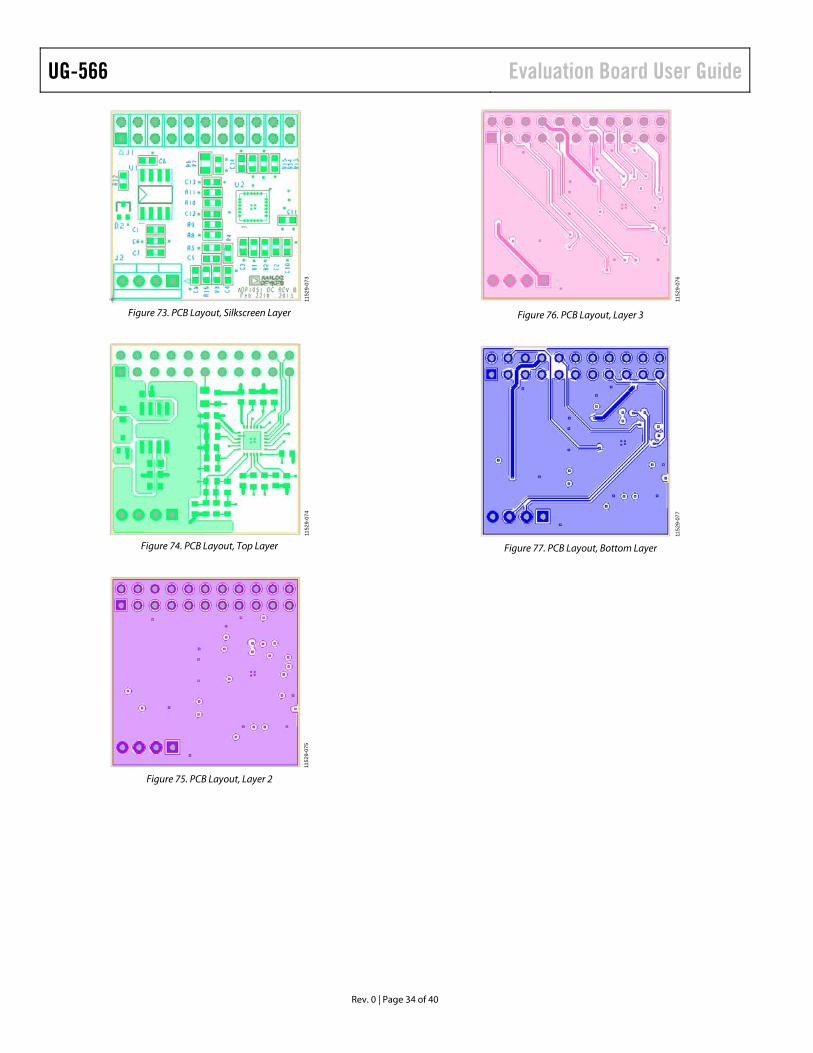
Rev. 0 | Page 33 of 40
1152
9-07
1
Figure 71. PCB Layout, Bottom Layout
ADP1051DC1-EVALZ
J1
CONN HEADERFEMALE 22PIN
10V1
VS–2
VS+3
CS2-4
CS2+5
VF6
CS17
SR18
SR29
OUTA10
OUTB11
OUTC12
OUTD13
SCL14
SDA15
PSON16
PGOOD17
FLAGIN18
3.3V19
AGND20
RTD21
OVP22
OUTA
OVP
C100.1µF/25V
00
SCL
SDA
0.1% RESISTOR
0.1% RESISTOR
0.1% RESISTOR
0.1% RESISTOR
0
0
SDASCL
3.3V
R16
10Ω
CS2–
CS2+
VS–
VS+
10V
SR2
OUTB
OUTD
OUTC
SR1
R132.2kΩ
C1
0.1µF/25V
C2
NC
C9
0.1µF/25V
C7
2.2µF/10V
J2
CONN HEADER4POS
1
234
R4
11kΩ
R8
11kΩ
R14
2.2kΩ
R12 2Ω
12
R3
200Ω
D2
200mA/70V
R51kΩ
R2 4.99kΩU1
ADP3303
OUT11
OUT22
NR3
GND4
#SD5
#ERR6
IN17
IN28
C5 1nF/50V
C14
330nF/50V
R9
1kΩ
C41nF/50V
C12
100pF/50V
R6 19.1kΩ
R10 10kΩ
PSON
C11
100pF/50V
R15 2.2kΩ
R11 10kΩ
R1 4.99kΩ
C60.1µF/25V
C3
NC
C8
1µF/16V
R7 1kΩ
10V_VCC
0
3.3V
0
3.3V
0
PGOOD
CS1
U2
ADP1051
VS
–1
VS
+2
CS
2–
3
CS
2+
4
VF
5
CS
16
SR17
SR28
OUTA9
OUTB10
OUTC11
OUTD12
SY
NC
I/F
LG
I1
3
SC
L1
4
SD
A1
5
CT
RL
16
PG
/AL
T#
17
VC
OR
E1
8
VDD19
AGND20
RES21
ADD22
RTD23
OVP24
0
FLAGIN3.3V
C13 0.1µF/25V3.3V
0.1% RESISTOR
RTD
VF
10V
0
0
0
1152
9-07
2
Figure 72. ADP1051 Daughter Schematic
UG-566 Evaluation Board User Guide
Rev. 0 | Page 34 of 40
1152
9-07
3
Figure 73. PCB Layout, Silkscreen Layer
1152
9-07
4
Figure 74. PCB Layout, Top Layer
1152
9-07
5
Figure 75. PCB Layout, Layer 2
1152
9-07
6
Figure 76. PCB Layout, Layer 3
1152
9-07
7
Figure 77. PCB Layout, Bottom Layer

Evaluation Board User Guide UG-566
Rev. 0 | Page 35 of 40
CURRENT SHARE DAUGHTER CARD
R44 1kΩ
R45 1kΩ
D2
1PS79SB31
21
R13
169kΩ
VSENSE
VSENSER125.11kΩ
3V3_SECR7 33.2kΩ
R9 33.2kΩ
0
10V_SEC
R18
20.5kΩ
R5 1MΩ
OPC
0
D1
1PS79SB31
21
U1ADA4851-4
+IN25 –VS
11+VS
4
–IN413
–IN12
+IN412
+IN13
–IN39
OUT414
+IN310
OUT38
OUT27
OUT11
–IN26
R17 169kΩ
VSENSE
R10 5.11kΩ
R4 66.5kΩ
R11
66.5kΩ
0
R2
1MΩR3
100kΩ
OPC
R16
169kΩ
3V3_SEC
CS2–
CS2+
R15
169kΩ
C24
0.1µF/25V
R14
2kΩ
IBUS
0CS2+CS2–
10V_SEC3V3_SEC
IBUSVF_ISHARE
AGNDAGND
R1
51kΩVF_ISHARE
J1
8 POS
12345678
C230.1µF/25V
C46 10nF/50V
C4710nF/50V
1152
9-07
8
Figure 78. Current Share Daughter Card Schematic
1152
9-07
9
Figure 79. PCB Layout, Silkscreen Layer
1152
9-08
0
Figure 80. PCB Layout, Top Layer
1152
9-08
1
Figure 81. PCB Layout, Layer 2

UG-566 Evaluation Board User Guide
Rev. 0 | Page 36 of 40
1152
9-08
2
Figure 82. PCB Layout, Layer 3
1152
9-08
3
Figure 83. PCB Layout, Bottom Layer

Evaluation Board User Guide UG-566
Rev. 0 | Page 37 of 40
ORDERING INFORMATION BILL OF MATERIALS
Table 10. ADP1051 Evaluation Board
Qty Reference Designator
Part Number
Footprint Description Manufacturer Digi-Key1
2 C1, C2 EEEFK2A221AM PCE4866TR-ND SMC-AEC-TG-K16 Capacitor ALUM 220 μF 100 V 20% SMD 8 C3, C4, C5, C6, C17,
C18, C49, C50 C3225X7R2A225K 445-4497-2-ND C1210 Capacitor 2.2 μF/100 V X7R 1210
6 C8, C9, C12, C14, C15, C16
GRM32ER71H475KA88 490-1864-2-ND C1210 Capacitor ceramic 4.7 μF 50 V 10% X7R 1210
2 C10, C11 EEEFK1V471AQ PCE4862TR-ND AL_CAP_H13 Capacitor ALUM 470 μF 35 V 20% SMD 2 C13, C85 C3225X7R2A225K 445-4497-2-ND C1210 Capacitor ceramic 2.2 μF 100 V 10% X7R 1210 6 C22, C26, C27,
C45, C56, C61 C2012X7R1E105K 445-1354-2-ND C0805 Capacitor ceramic 1 μF 25 V 10% X7R 0805
9 C23, C24, C25, C28, C29, C30, C43, C44, C57
C1608X7R1E104K 445-1316-2-ND C0603 Capacitor ceramic 0.1 μF 25 V 10% X7R 0603
1 C31 C1608X7R1H104K 445-1314-2-ND C0603 Capacitor ceramic 0.1μF 50 V 10% X7R 0603 2 C32, C36 C1608COG1H330J 445-1257-2-ND C0603 Capacitor ceramic 33 pF 50 V 5% NP0 0603 2 C34, C35 C1608COG1H101J 445-1281-2-ND C0603 Capacitor ceramic 100 pF 50 V 5% NP0 0603 4 C38, C39, C40, C41 C1608COG1H102J 445-1293-2-ND C0603 Capacitor ceramic 1000 pF 50 V 5% NP0 0603 1 C42 C1608X7R1H104K 445-1314-2-ND C0603 Capacitor ceramic 0.1 μF 50 V 10% X7R 0603 4 C46, C47, C48, C72 C1608X7R1H103J 445-5089-2-ND C0603 Capacitor ceramic 10 nF 50 V 5% X7R 0603 1 C51 C1608C0G2E471J 445-2318-2-ND C0603 Capacitor ceramic 470 pF 250 V 5% NP0 0603 1 C52 C2012X7R2A104K 445-1418-2-ND C0805 Capacitor ceramic 0.1 μF 100 V 10% X7R 0805 4 C53, C54, C58, C60 C3216X7R1C106K 445-4042-2-ND C1206 Capacitor ceramic 10 μF 16 V 10% X7R 1206 1 C55 C1608C0G1H391J 445-1288-2-ND C0603 Capacitor ceramic 390 pF 50 V 5% NP0 0603 1 C59 C1608COG1H102J 445-1293-2-ND C0603 Capacitor ceramic 1 nF 50 V 5% NP0 0603 1 C62 C1608COG2A221J 445-2308-2-ND C0603 Capacitor ceramic 220 pF 100 V 5% NP0 0603 1 C63 202S43W102KV4E 709-1053-2-ND C1812 Capacitor ceramic 1 nF 2 KV 10% X7R 1812 6 C64, C65, C66,
C67, C68, C69 C3225X7R1H335K 445-3936-2-ND C1210 Capacitor ceramic 3.3 μF 50 V 10% X7R 1210
2 C70, C71 C2012X7R2E103K 445-2280-2-ND C0805 Capacitor ceramic 10 nF 250 V X7R 0805 9 D1, D2, D4, D5, D6,
D9, D10, D11, D20 MBR130LSFT1G MBR130LSFT1GOSTR-ND SOD123 Schottky diode 1 A 30 V SOD-123FL
9 D3, D8, D12, D22, D24, D32, D33, D34, D35
MURA110T3G MURA110T3GOSTR-ND SMA Diode ultrafast 2 A 100 V SMA
3 D7, D17, D18 CMD15-21UBC/TR8 L62206CT-ND D1206 LED blue clear 1206 SMD 2 D13, D15 BAV99 BAV99FSTR-ND SOT23 Diode ultrafast HI COND 70 V SOT-23 3 D14, D21, D37 BAV70WT1G BAV70WT1GOSTR-ND SOT323 Diode switch dual CC 70 V SOT323 13 D16, D28, D31, D36,
D38, D39, D40, D43, D44, D45, D46, D51, D52
BAT42WS-7 BAT42WSDITR-ND SOD323 Schottky diode 30 V 200MW SOD-323
1 D19 ZR431F01TA ZR431F01TR-ND SOT23-IC IC VREF shunt PREC ADJ SOT-23 1 D23 MMBD1504A MMBD1504ATR-ND SOT23 Diode SS 200 V 200 MA SOT23 1 D25 EGL34B-E3/83 EGL34B-E3/83-ND DO-213AA Diode 0.5A 100 V 50 NS MELF 1 D26 MMBZ5231BLT1G MMBZ5231BLT1GOSTR-ND SOT23 Diode Zener 5.1 V 225 MW SOT-23 3 D29, D30, D41 BAT42WS-7 BAT42WSDITR-ND SOD323 Schottky diode 30 V 200 MW SOD-323 9 JP1, JP2, JP3, JP4, JP5,
JP11, JP12, JP13, JP14 STC02SYAN S9000-ND HEADER-SR-2 Connector jumper shorting tin
1 JP9 N/A N/A Shortpin Single connect point of AGND and PGND 4 J1, J2, J5, J6 108-0740-001 J147-ND B-JACK Connector jack banana 4 J3, J4, J12, J13 N/A N/A PADJUMPER Power connector jumper on PCB 1 J8 TSW-111-14-T-D SAM1058-11-ND HEADER-DR-22 Connector header 22POS 0.100 dual tin 22
male pin 2.54 1 J15 PPC081LFBN-RC S4108-ND HEADER-I-SR-8 Single row 8 female pin 2.54 mm 2 J17, J18 75869-132LF 609-3530-ND 313-208-s2 Connector header 8POS dual vert PCB 1 L1 IHLP5050FDER1R0M01 541-1032-2-ND IND-IHLP-5050FD Power inductor 1.0 μH 32 A SMD 1 L2 #7443630420 N/A LER-20-63 Power inductor 4.2uH 24 A 3.04 mΩ SMD
LER-20-63 N/A Power Inductor 3.6 μH 30 A 2.3 mΩ SMD 1 L3 IHLP2525EZERR56M01 IHLP2525EZERR56M01-ND 2525ez power Inductor 0.56 μH 20 A SMD

UG-566 Evaluation Board User Guide
Rev. 0 | Page 38 of 40
Qty Reference Designator
Part Number
Footprint Description Manufacturer Digi-Key1
5 MH1, MH2, MH3, MH4, MH5
R30-1011602 952-1492-ND MH Standoff HEX M3 THR Brass 16 mm
8 QA, QB, QC, QD, Q3, Q4, Q7, Q8
IPD068N10N3 G IPD068N10N3 G-ND DPAK MOSFET N-CH 100 V 90 A TO252-3
1 Q9 BSS138 BSS138TR-ND SOT23 MOSFET N-CH 50 V 220 MA SOT-23 1 Q10 MMBT2907A MMBT2907AFSTR-ND SOT23 Transistor GP PNP AMP SOT-23 1 RT1 NCP15WF104F03RC 490-4803-2-ND R0402 Thermistor 100 kΩ NTC 0402 SMD
resistance 1% beta 12 R2, R5, R7, R8, R21,
R22, R24, R67, R77, R85, R96, R98
CRCW060310K0JNTA CRCW060310K0JNTA-ND R0603 Resistor 10 kΩ 5% 1/10 W 0603 SMD
2 R3, R23 ERJ-M1WTF2M0U P2.0NDTR-ND R2512 Resistor 0.002 Ω 1 W 1% 2512 8 R1, R4, R6, R9, R11,
R19, R20, R25 CRCW08052R00JNEA 541-2.0ATR-ND R0805 Resistor 2 Ω 5% 1/8 W 0805 SMD
1 R10 CRCW060310K0JNTA CRCW060310K0JNTA-ND R0603 Resistor 10 kΩ 5% 1/10 W 0603 SMD 1 R14 CRCW120630K1FKEA 541-30.1KFTR-ND R1206 Resistor 30.1 kΩ 1/4 W 1% 1206 SMD 2 R26, R32 CRCW08050000Z0EA 541-0.0ATR-ND R0805 Resistor 0.0 Ω 1/8 W 0805 SMD 19 R27, R30, R33, R34,
R35, R47, R48, R54, R57, R59, R70, R73, R91, R92, R93, R94, R95, R105, R123
CRCW06030000Z0EA 541-0.0GTR-ND R0603 Resistor 0.0 Ω 1/10 W 0603 SMD
9 R31, R36, R37, R49, R58, R60, R107, R111, R140
CRCW06030000Z0EA 541-0.0GTR-ND R0603 Resistor 0.0 Ω 1/10 W 0603 SMD
1 R38 CRCW0603100RFKEA 541-100HCT-ND R0603 Resistor 100 Ω 1/10 W 1% 0603 SMD 2 R39, R40 CRCW080510R0FKEA 541-10.0CTR-ND R0805 Resistor 10.0 Ω 1/8 W 1% 0805 SMD 4 R41, R43, R46, R53 CRCW060310R0FKEA 541-10.0HTR-ND R0603 Resistor 10.0 Ω 1/10 W 1% 0603 SMD 2 R45, R102 CRCW06034K10JNEA 541-4.7KGCT-ND R0603 Resistor 4.7 kΩ 1/10 W 5% 0603 SMD 1 R50 CRCW060316K5FKTA CRCW060316K5FKTA-ND R0603 Resistor 16.5 kΩ 1% 1/10 W 0603 SMD 4 R51, R56, R64, R69 CRCW06031K00FKEA 541-1.00KHCT-ND R0603 Resistor 1.00 kΩ 1/10 W 1% 0603 SMD 1 R52 CRCW06031K00FKEA 541-1.00KHCT-ND R0603 Resistor 1.00 kΩ 1/10 W 1% 0603 SMD 1 R63 CRCW0603220KFKEA 541-220KHTR-ND R0603 Resistor 220 kΩ 1/10 W 1% 0603 SMD 3 R65, R72, R75 CRCW06035K10JNEA 541-5.1KGCT-ND R0603 Resistor 5.1 kΩ 1/10 W 5% 0603 SMD 1 R66 CRCW0805100KJNEA 541-100KATR-ND R0805 Resistor 100 kΩ 1/8 W 5% 0805 SMD 1 R68 CRCW06038K20FKEA 541-8.20KHCT-ND R0603 Resistor 8.20 kΩ 1/10 W 1% 0603 SMD 3 R71, R76, R106 CRCW0603220RJNEA 541-220GCT-ND R0603 Resistor 220 Ω 1/10W 5% 0603 SMD 2 R74, R99 CRCW08051R00JNEA 541-1.0ATR-ND R0805 Resistor 1 Ω 5% 1/8W 0805 2 R78, R79 CRCW080520R0JNEA 541-20ACT-ND R0805 Resistor 20 Ω 1/8 W 5% 0805 SMD 1 R80 CRCW060314K0FKEA 541-14.0KHTR-ND R0603 Resistor 14.0 kΩ 1/10 W 1% 0603 SMD 1 R81 CRCW08051M00FKEA 541-1.00MCTR-ND R0805 Resistor 1.00 M Ω 1/8 W 1% 0805 SMD 2 R82, R83 CRCW0805680RJNEA 541-680ACT-ND R0805 Resistor 680 Ω 1/8 W 5% 0805 SMD 1 R84 CRCW06035K10FKEA 541-5.10KHTR-ND R0603 Resistor 5.10 kΩ 1/10 W 1% 0603 SMD 1 R86 CRCW060354K9FKEA 541-54.9KHTR-ND R0603 Resistor 54.9 kΩ 1/10 W 1% 0603 SMD 1 R87 CRCW060336K0FKEA 541-36.0KHTR-ND R0603 Resistor 36.0 kΩ 1/10 W 1% 0603 SMD 10 R88, R89, R90, R100,
R101, R103, R104, R108, R109, R110
CRCW120620K0JNEA 541-20KETR-ND R1206 Resistor 20 kΩ 1/4 W 5% 1206 SMD
1 R97 CRCW080510K0JNEA 541-10KATR-ND R0805 Resistor 10 kΩ 1/8 W 5% 0805 SMD 3 SW1, SW2, SW3 EG1218 EG1903-ND SPDT-SLSW Switch slide SPDT 30 V.2A PC MNT

Evaluation Board User Guide UG-566
Rev. 0 | Page 39 of 40
Qty Reference Designator
Part Number
Footprint Description Manufacturer Digi-Key1
43 TP1, TP3, TP4, TP5, TP6, TP7, TP8, TP9, TP10, TP11, TP12, TP13, TP14, TP15, TP16, TP17, TP18, TP19, TP20, TP21, TP22, TP23, TP24, TP25, TP26, TP27, TP28, TP29, TP30, TP33, TP34, TP35, TP36, TP37, TP38, TP40, TP41, TP42, TP47, TP48, TP49, TP50, TP51
5010 5010K-ND TP-70 Test point PC
3 TP39, TP44, TP45 GTP002 N/A TP-70 dual Ground test point 1 T1 PA1005.100NL 553-1529-2-ND P820X XFRMR current sense 2.0 MH 1:100 SMD 1 T2 #750341378 N/A BDC_2512 Transformer ER25 5:2:2
BDC-25-69 N/A Transformer ER25 5:2:2 1 T3 #750341379 N/A PBSER9-77 36 V to 75 V input, 12 V 0.25 A pri output,
12 V, 0.25 A sec output, ER9.5 22:8:8 BSER9-77 N/A 36 V to 75 V input, 12 V pri output, 12 V sec
output, ER9.5 22:8:8 1 T4 PA1005.100NL 553-1529-2-ND P820X XFRMR current sense 2.0 MH 1:100 SMD 2 U1, U4 HIP2101EIBZT HIP2101EIBZTTR-ND 8-SOIC-EP IC driver half bridge 100 V 8EPSOIC 3 U2, U5, U7 ADUM3210BRZ-RL7 ADUM3210BRZ-RL7TR-ND 8-SOIC iCoupler 2CH 8-SOIC 1 U3 ADP3654ARDZ-R7 ADP3654ARDZ-R7-ND 8-SOIC_N_EP IC MOSFET DVR 4 A dual HS SOIC_N_EP 1 U14 NCP1031DR2G NCP1031DR2GOSTR-ND 8-SOIC IC CTRLR PWM OTP OVD HV 8SOIC 1 N/A = not applicable.
Table 11. ADP1051 Daughter Card
Qty Reference Designator
Part Number
Footprint Description Manufacturer Digi-Key1
5 C1, C6, C9, C10, C13 C1608X7R1H104K 445-1316-2-ND C0603 Capacitor ceramic 0.1 μF 25 V 10% X7R 0603 2 C2, C3 C1608X7R1H104K 445-1316-2-ND C0603 Capacitor ceramic 0.1 μF 25 V 10% X7R 0603 2 C4, C5 C1608COG1H102J 445-1293-2-ND C0603 Capacitor ceramic 1 nF 50 V 5% NP0 0603 1 C7 C1608X7R1A225K 445-5958-6-ND C0603 Capacitor ceramic 2.2 μF 10 V 10% X7R 0603 1 C8 C1608X7R1C105K 445-1604-2-ND C0603 Capacitor ceramic 1 μF 16 V 10% X7R 0603 2 C11, C12 C1608COG1H101J 445-1281-2-ND C0603 Capacitor ceramic 100 pF 50 V 5% NP0 0603 1 C14 C1608X7R1H334K 445-5950-2-ND C0603 Capacitor ceramic 330 nF 50 V 10% X7R 0603 1 D2 BAV70WT1G BAV70WT1GOSTR-ND SOT323 Diode switch dual CC 70 V SOT323 1 J1 PPPC112LFBN-RC S7114-ND Header-dr-22 Connector header FMAL 22PS.1" DL gold 1 J2 69167-104HLF 609-2411-ND HEADER-L-SR-4 Connector header 4POS SGL PCB 30GOLD 2 R1, R2 9-1879360-4 9-1879360-4-ND R0603 Resistor 4.99 kΩ 1/16 W 0.1% 0603 10PPM 1 R3 CRCW0603200RFKEA 541-200HTR-ND R0603 Resistor 200 Ω 1/10 W 1% 0603 SMD 1 R4 TNPW060311K0BEEA TNP11.0KAATR-ND R0603 Resistor 11 kΩ 1/10 W 0.1% 0603 SMD 1 R5 TNPW06031K00BEEA TNP1.00KAATR-ND R0603 Resistor 1.00 kΩ 1/10 W 0.1% 0603 SMD 1 R6 CRCW080519K1FKEA 541-19.1KCTR-ND R0805 Resistor 19.1 kΩ 1/8 W 1% 0805 SMD 2 R7, R9 CRCW06031K00FKEA 541-1.00KHCT-ND R0603 Resistor 1.00 kΩ 1/10 W 1% 0603 SMD 1 R8 CRCW060311K0FKEA 541-11.0KHTR-ND R0603 Resistor 11 kΩ 1/10 W 1% 0603 SMD 1 R10 CRCW060310K0FKEA 541-10.0KHTR-ND R0603 Resistor 10 kΩ 1% 1/10 W 0603 SMD 1 R11 TNPW060310K0BEEA TNP10.0KAATR-ND R0603 Resistor 10 kΩ 0.1% 1/10 W 0603 SMD 1 R12 CRCW06032R00FKEA 541-2.00HHTR-ND R0603 Resistor 2 Ω 1% 1/10 W 0603 SMD 3 R13, R14, R15 CRCW06032K20FKEA 541-2.20KHTR-ND R0603 Resistor 2.2 kΩ 1% 1/10 W 0603 SMD 1 R16 CRCW060310R0FKEA 541-10.0HTR-ND R0603 Resistor 10 Ω 1% 1/10 W 0603 SMD 1 U1 ADP3303ARZ-3.3 ADP3303ARZ-3.3-ND SO8 IC regulator LDO 200 MA 3.3 V 8-SOIC 1 U2 ADP1051ACPZ N/A CP-24-7 Digital controller ADP1051 CP-24-7 1 N/A = not applicable.

UG-566 Evaluation Board User Guide
Rev. 0 | Page 40 of 40
Table 12. Current Share Daughter Card
Qty Reference Designator
Part Number
Footprint Description Manufacturer Digi-Key 2 C23, C24 C1608X7R1H104K 445-1316-2-ND C0603 Capacitor ceramic 0.1 μF 25 V 10% X7R 0603 2 C46, C47 C1608X7R1H103J 445-5089-2-ND C0603 Capacitor ceramic 10000 pF 50 V 5% X7R 0603 2 D1, D2 1PS79SB31 1PS79SB31,315-ND SOD523 Diode Schottky 30 V 200 mA SC-79 1 J1 PPC081LFBN-RC 09-3321-ND HEADER-SR-8 CONN HEADER 8POS 0.100 R/A 15AU 1 R1 CRCW060351K0FKEA 541-51.0KHTR-ND R0603 Resistor 51.0 kΩ 1/10 W 1% 0603 SMD 2 R2, R5 CRCW06031M00FKEA 541-1.00MHTR-ND R0603 Resistor 1.00 MΩ 1/10 W 1% 0603 SMD 1 R3 CRCW0603100KFKEA 541-100KHTR-ND R0603 Resistor 100 kΩ 1/10 W 1% 0603 SMD 2 R4, R11 CRCW060366K5FKEA 541-66.5KHTR-ND R0603 Resistor 66.5 kΩ 1/10 W 1% 0603 SMD 2 R7, R9 CRCW060333K2FKEA 541-33.2KHTR-ND R0603 Resistor 33.2 kΩ 1/10 W 1% 0603 SMD 2 R10, R12 CRCW06035K11FKEA 541-5.11KHTR-ND R0603 Resistor 5.11 kΩ 1/10 W 1% 0603 SMD 4 R13, R15, R16, R17 CRCW0603169KFKEA 541-169KHTR-ND R0603 Resistor 169 kΩ 1/10 W 1% 0603 SMD 1 R14 CRCW06032K00FKEA 541-2.00KHTR-ND R0603 Resistor 2.00 kΩ 1/10 W 1% 0603 SMD 1 R18 CRCW060320K5FKEA 541-20.5KHTR-ND R0603 Resistor 20.5 kΩ 1/10 W 1% 0603 SMD 2 R44, R45 CRCW06031K00FKEA 541-1.00KHCT-ND R0603 Resistor 1.00 kΩ 1/10 W 1% 0603 SMD 1 U1 ADA4851-4YRUZ ADA4851-4YRUZ-ND TSSOP14 IC op amp VF R-R quad LP 14-lead TSSOP
ESD Caution ESD (electrostatic discharge) sensitive device. Charged devices and circuit boards can discharge without detection. Although this product features patented or proprietary protection circuitry, damage may occur on devices subjected to high energy ESD. Therefore, proper ESD precautions should be taken to avoid performance degradation or loss of functionality.
Legal Terms and Conditions By using the evaluation board discussed herein (together with any tools, components documentation or support materials, the “Evaluation Board”), you are agreeing to be bound by the terms and conditions set forth below (“Agreement”) unless you have purchased the Evaluation Board, in which case the Analog Devices Standard Terms and Conditions of Sale shall govern. Do not use the Evaluation Board until you have read and agreed to the Agreement. Your use of the Evaluation Board shall signify your acceptance of the Agreement. This Agreement is made by and between you (“Customer”) and Analog Devices, Inc. (“ADI”), with its principal place of business at One Technology Way, Norwood, MA 02062, USA. Subject to the terms and conditions of the Agreement, ADI hereby grants to Customer a free, limited, personal, temporary, non-exclusive, non-sublicensable, non-transferable license to use the Evaluation Board FOR EVALUATION PURPOSES ONLY. Customer understands and agrees that the Evaluation Board is provided for the sole and exclusive purpose referenced above, and agrees not to use the Evaluation Board for any other purpose. Furthermore, the license granted is expressly made subject to the following additional limitations: Customer shall not (i) rent, lease, display, sell, transfer, assign, sublicense, or distribute the Evaluation Board; and (ii) permit any Third Party to access the Evaluation Board. As used herein, the term “Third Party” includes any entity other than ADI, Customer, their employees, affiliates and in-house consultants. The Evaluation Board is NOT sold to Customer; all rights not expressly granted herein, including ownership of the Evaluation Board, are reserved by ADI. CONFIDENTIALITY. This Agreement and the Evaluation Board shall all be considered the confidential and proprietary information of ADI. Customer may not disclose or transfer any portion of the Evaluation Board to any other party for any reason. Upon discontinuation of use of the Evaluation Board or termination of this Agreement, Customer agrees to promptly return the Evaluation Board to ADI. ADDITIONAL RESTRICTIONS. Customer may not disassemble, decompile or reverse engineer chips on the Evaluation Board. Customer shall inform ADI of any occurred damages or any modifications or alterations it makes to the Evaluation Board, including but not limited to soldering or any other activity that affects the material content of the Evaluation Board. Modifications to the Evaluation Board must comply with applicable law, including but not limited to the RoHS Directive. TERMINATION. ADI may terminate this Agreement at any time upon giving written notice to Customer. Customer agrees to return to ADI the Evaluation Board at that time. LIMITATION OF LIABILITY. THE EVALUATION BOARD PROVIDED HEREUNDER IS PROVIDED “AS IS” AND ADI MAKES NO WARRANTIES OR REPRESENTATIONS OF ANY KIND WITH RESPECT TO IT. ADI SPECIFICALLY DISCLAIMS ANY REPRESENTATIONS, ENDORSEMENTS, GUARANTEES, OR WARRANTIES, EXPRESS OR IMPLIED, RELATED TO THE EVALUATION BOARD INCLUDING, BUT NOT LIMITED TO, THE IMPLIED WARRANTY OF MERCHANTABILITY, TITLE, FITNESS FOR A PARTICULAR PURPOSE OR NONINFRINGEMENT OF INTELLECTUAL PROPERTY RIGHTS. IN NO EVENT WILL ADI AND ITS LICENSORS BE LIABLE FOR ANY INCIDENTAL, SPECIAL, INDIRECT, OR CONSEQUENTIAL DAMAGES RESULTING FROM CUSTOMER’S POSSESSION OR USE OF THE EVALUATION BOARD, INCLUDING BUT NOT LIMITED TO LOST PROFITS, DELAY COSTS, LABOR COSTS OR LOSS OF GOODWILL. ADI’S TOTAL LIABILITY FROM ANY AND ALL CAUSES SHALL BE LIMITED TO THE AMOUNT OF ONE HUNDRED US DOLLARS ($100.00). EXPORT. Customer agrees that it will not directly or indirectly export the Evaluation Board to another country, and that it will comply with all applicable United States federal laws and regulations relating to exports. GOVERNING LAW. This Agreement shall be governed by and construed in accordance with the substantive laws of the Commonwealth of Massachusetts (excluding conflict of law rules). Any legal action regarding this Agreement will be heard in the state or federal courts having jurisdiction in Suffolk County, Massachusetts, and Customer hereby submits to the personal jurisdiction and venue of such courts. The United Nations Convention on Contracts for the International Sale of Goods shall not apply to this Agreement and is expressly disclaimed.
©2013 Analog Devices, Inc. All rights reserved. Trademarks and registered trademarks are the property of their respective owners. UG11529-0-7/13(0)