evaluating the effectiveness of a cdm esd control program · evaluating the effectiveness of a cdm...
TRANSCRIPT
Proc. ESA Annual Meeting on Electrostatics 2010, Paper L2
Evaluating the Effectiveness of a CDM ESD Control Program
Arnold Steinman, M.S.E.E.
Electronics Workshop Trek Inc.
Dangelmayer Associates Phone: (1) 510-549-3775
e-mail: [email protected]
Abstract—Electric fields from charged semiconductor device packages or nearby charged insulators cause Charged Device Model (CDM) electrostatic discharge (ESD) events, when the device leads touch ground. Exposure to CDM ESD occurs primarily in the assembly, packaging, and test areas of semiconductor manufacturing, as well as in assembly areas of electronics contract manufacturing. Device design and proper handling methods, combined with static control methods, can prevent the rapid and damaging discharge to packaged devices. A complete static control program includes grounding methods, proper material selection, and ionization to neutralize charge on insulators. While this may be sufficient to prevent Human Body Model (HBM) ESD damage, more is needed to eliminate CDM ESD. Additional measurements to target the locations of CDM ESD, elimination of metal-to-metal contact, and monitoring to verify the effectiveness of the CDM ESD program are all required.
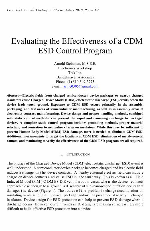
I. INTRODUCTION The physics of the Char ged Device Model (CDM) electrostatic discharge (ESD) event is well understood. A semiconductor device package becomes charged and its electric field induces a c harge on t he device contacts. A nearby e xternal elect ric field can induc e charge on de vice contacts a nd cause ESD in the sam e way. T his is known as a Field Induced M odel (FIM ) C DM ES D E vent. I n bot h cases, whe n the device contacts approach close enough to a ground, a d ischarge of sub- nanosecond duration occurs that damages t he device (Figure 1). The s ource o f t he problem i s char ge a ccumulation on insulating m aterial of the device package and/or the prese nce of nearby charged insulators. Device design for ESD protection can help to prevent ESD damage when a discharge occurs. However, current trends in IC design are making it increasingly more difficult to build effective ESD protection into a device.
Proc. ESA Annual Meeting on Electrostatics 2010 2
Charged Package ++ ++ ++
ESD
Conductive Apparatus
Mobile Charge
on Lead Frame
Immobile
Charge on
Plastic ++ ++ ++
Fig. 1. CDM ESD Event caused by charged device package. Smaller feature sizes, higher pin counts and higher operating speeds make designs that provide ade quate prot ection agai nst ES D si gnificantly h arder to achieve. [1] It is therefore unreasonable to depend solely on device design solutions to solve CDM ESD problems. More effective static con trol methods that prevent the buildup of static ch arge must also be implemented in the production environment.
II. SOLVING THE CDM ESD PROBLEM FOR DEVICES Control of ESD is required in all stages of device manufacture, including when inserting devices in circuit boards, when inserting circuit boards in equipment and l arge systems, and anytim e electronic sys tems need se rvicing. Indee d, t riboelectric static char ge generation i s a lmost unavoidable during device or ci rcuit board handling. Contact with other m aterials, re gardless o f whether t hose materials are in sulators or con ductors or whether or not they are gro unded, will easi ly pass charge to the in sulating material in a device package or circuit board. Devices should not be placed in proximity to or pass near any charged objects. Ideally, insulators or un grounded conductors should be kept at least 3 0 cm away fro m sensitive parts or they should be provided with electrostatic shielding. Devices can be affected by electric fields from cha rged pa rts previ ously placed on a circuit boa rd. In fact, the additional parts that are connected to a device once it is placed in a ci rcuit board increase the overall capacitance that determines the maximum static charge accumulation. If a lead of any component on the circuit board touches ground, a CDM-like discharge may occur. This type of discharge, known as a Charged Board Event (CBE), is currently under study. The higher capacitance and greater accumulated charge involved in CBE-type discharges often results i n m uch m ore severe device damage t han t hat occurring i n a C DM E SD event. It is easily mistaken for ESD damage accountable by other models. Device design

Proc. ESA Annual Meeting on Electrostatics 2010 3
for CDM-type discharge prevention cannot provide protection for the higher capacitance discharge of t he CBE type. The sam e ESD mitigation m ethods used to pre vent CDM ESD events are useful in preventing CBE. Since CDM ESD events occur when a device lead contacts ground, a risk of CDM-type events be gins i n Wafer Probe at t he e nd o f sem iconductor f rontend p rocessing a nd continues t hroughout th e assem bly, p ackaging and test p rocesses in b ackend manufacturing. Th e device is th us at h azard t o C DM ESD until it i s con tained in static-protective p ackaging fo r shipment to th e cu stomer. A further risk o f CDM ESD damage exi sts w hen t he c ustomer rem oves t he de vice f rom t he s tatic-protective packaging and places it in a circuit board or other location. Once a device is placed on the circuit board, ESD damage is rarely du e to a C DM ESD event. ESD d amage to circu it board mounted components may be CBE, or characterized by other ESD damage models. Given th e v aried env ironments th e device passes thro ugh, it is unreasonable to ex pect device design to provide complete protection from ESD. Indeed, protection alone, either through d esign or t hrough static co ntrol grounding m ethods, is i nsufficient without charge elimination from the device environment.
III. STATIC CHARGE CONTROL Since t he l ate 1970’s t he understanding of p revention and protection from ESD e vents and ESD con trol through device design has been improving. However, functionality and feature size issues continue to challenge design for ESD control. Higher device operating speeds make the design of ESD protection networks more di fficult and large pin count devices limit the die area available for the protection networks. Feature sizes keep rapidly shrinking to i ncrease d evice fun ctionality an d in crease manufacturing p rofitability, but the area needed to d issipate the energy of ESD events does not change accordingly. As the res ult, the ESD designers are as king t o reduce user expectations for on-c hip ESD protection, pa rticularly due t o signific ant im provements and wide acce ptance of ESD control programs throughout the electronics industry. [1] The understanding of ESD control is improving. This improvement was stimulated by the needs of hard disk drive (HDD) manufacturing in the late 1990’s. Magneto-resistive (MR) read head techn ology in troduced an essen tial electro nic part th at was sen sitive to both Human B ody M odel (HBM) a nd C DM ES D e vents o f 25 volts or l ess. De sign improvements that increase d the st orage cap acity of t he H DD by several orders of magnitude lowered the voltage sensitivity for ESD even further. As a consequence, HDD factories now reliably control ESD levels below 5 volts and in some cases below 1 volt. Few sem iconductors need ESD co ntrols at th is lev el at th is ti me, b ut th e HDD manufacturing results show that it is achievable. The methods for strict control of electrostatic potential in HDD manufacturing developed because no design solution was available to mitigate CDM ESD problems. Once this was recognized the devel opment of a c omplete static control progra m became an industry
Proc. ESA Annual Meeting on Electrostatics 2010 4
focus. Today, the production of disk drives without a co mplete static con trol program is not a possibility. As feature sizes sh rink on sem iconductor devices, HDD-style ESD control m ay b e n eeded in t he photolithography areas wh ere reticles are h andled. [2] Future design changes in semiconductor devices may also require more extensive static control programs.
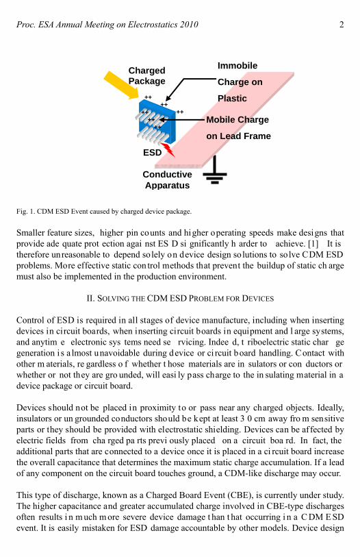
IV. MODIFYING THE ESD CONTROL PROGRAM TO CONTROL CDM ESD ESD control involves preventing the generation, storage, or rapid transfer of static charge. Properly designed static control programs, such as ANSI ESD S20.20 and IEC 61340-5-1, include all the elem ents need ed to control static char ge and to pro tect 10 0-volt HBM sensitive devices. [3 ][4] Th ese program s fo cus on th e devices an d th eir env ironment, including the personnel that handle the devices. The focus of these programs is removing static ch arge fro m all ob jects in th e work area, b y conn ecting th em th rough a resistive path to ground. Grounding of pe rsonnel, worksurfaces, furniture, flooring, t ransport methods, and packaging eliminates charge transfer to ESD sensitive devices and provides some shielding from electric fields. The static control program uses resistance measuring devices to ve rify the c haracteristics and grounding of the ESD con trol m aterials. An example of such a measuring device and different probes for worksurfaces is sh own in Figure 2.
Fig. 2. Instruments for resistance measurement of worksurfaces To stop C DM ESD damage in more sensi tive devices, t he st atic co ntrol p rogram must expand i ts f ocus t o i nclude the device, t he a utomated e quipment use d t o handle t he device, and the en vironment in wh ich it is h andled. As in all static co ntrol p rograms, grounding methods and static dissipative materials prevent the generation and storage of static char ge. This ap proach, whe n a pplied t o a de vice, uses c onductive or dissipative
Proc. ESA Annual Meeting on Electrostatics 2010 5
carriers to maintain all d evice leads in contact with ground throughout the manufacture and handling of t he device. Ground co ntact i s oft en l ost, ho wever, when t he de vice i s removed f rom t he car rier f or different m anufacturing steps or for i nsertion i nto ci rcuit boards. Metal-to-metal contact betwee n the exposed device leads and grounded surfaces must be avoi ded and dissipative c ontact surfaces m ust replace c onductive surfac es whenever possible. Final device test p rovides a good example of the difficulties experienced in protecting a device from CDM ESD damage. Even if all device leads remained connected to ground during all m anufacturing steps leadi ng up to fi nal test, it is necessary that the device be removed from its carrier and inserted into a test socket during final test. At the moment of separation from the carrier , charge on t he insulative d evice p ackage is able to indu ce charge on the device l eads. This charge on the package may have come f rom previous manufacturing steps or from the physical act of picking up the device from its carrier. The device is next inserted into the metal contacts of the test socket. For testing purposes this is unavoidable and static dissipative contacts are not possible. CDM ESD events can occur at the instant of contact. Device damage may occur depending on the package size, package charge, and the level of device ESD protection built in to the device. Similarly, removing the device from the s ocket afte r test m ay g enerate ch arge on the test socket itself. Left unneutralized this charge may present an in creased CDM ESD hazard to the next device inserted in the test socket.
V. IONIZATION IN THE CDM ESD STATIC CONTROL PROGRAM Effective static con trol programs must also consider the charged insulators that a re the source of the CDM ESD problem. Device packages, process essential insulating surfaces in test so ckets, lab eling equ ipment, circ uit boards , packaging m aterials and ot her electronic components, al l contribute to t he CDM ESD problem. Properly designed ai r ionization, as a part o f an overall st atic cont rol p rogram, is t he key t o rem oving a ny accumulated char ge from these insulators. Leaving any static char ge in the de vice environment will only increase the likelihood of device failure. The proper application of ionizers requires that the ionized air come into contact with the charged s urface long e nough to ass ure charge n eutralization. This co nsideration is especially important for ESD control in high-speed manufacturing equipment. Only the topside of a device package may be neut ralized while the package is i n its carrier. Only when t he de vice i s picked u p ca n b oth si des be neutralized. Pi ckup a nd t ransport t ime needs to be long enough to assure sufficient device package neutralization. Ionization re moves st atic char ge f rom t he de vice pac kage and all objects in their immediate area. Th e possibility o f CDM ESD is all bu t eliminated i f t here is no static charge present . Thus, at a sm all incremental co st to a static con trol prog ram, air ionization eliminates the static char ge, com plementing the protective ef fects of device design for E SD a nd ot her protective grounding m easures. A n e xample of an i onizer
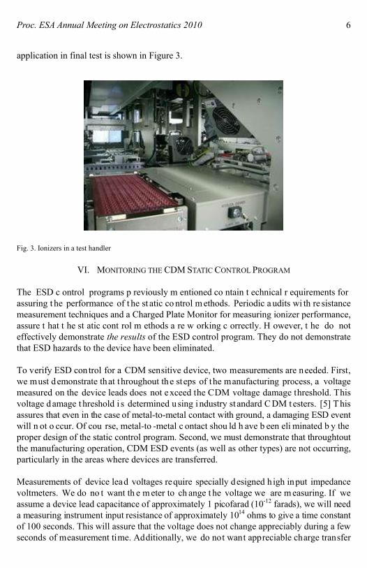
Proc. ESA Annual Meeting on Electrostatics 2010 6
application in final test is shown in Figure 3.
Fig. 3. Ionizers in a test handler
VI. MONITORING THE CDM STATIC CONTROL PROGRAM The ESD c ontrol programs p reviously m entioned co ntain t echnical r equirements for assuring t he performance of t he st atic co ntrol m ethods. Periodic a udits wi th re sistance measurement techniques and a Charged Plate Monitor for measuring ionizer performance, assure t hat t he st atic cont rol m ethods a re w orking c orrectly. H owever, t he do not effectively demonstrate the results of the ESD control program. They do not demonstrate that ESD hazards to the device have been eliminated. To verify ESD con trol for a CDM sensitive device, two measurements are needed. First, we must demonstrate that throughout the steps of the manufacturing process, a voltage measured on the device leads does not e xceed the CDM voltage damage threshold. This voltage d amage t hreshold i s determined u sing i ndustry st andard C DM t esters. [5] This assures that even in the case of metal-to-metal contact with ground, a damaging ESD event will n ot o ccur. Of cou rse, metal-to -metal c ontact shou ld h ave b een eli minated b y the proper design of the static control program. Second, we must demonstrate that throughtout the manufacturing operation, CDM ESD events (as well as other types) are not occurring, particularly in the areas where devices are transferred. Measurements of device lead voltages require specially designed h igh input impedance voltmeters. We do no t want th e m eter to ch ange t he voltage we are m easuring. If we assume a device lead capacitance of approximately 1 picofarad (10-12 farads), we will need a measuring instrument input resistance of approximately 1014 ohms to give a time constant of 100 seconds. This will assure that the voltage does not change appreciably during a few seconds of measurement time. Additionally, we do not want appreciable charge transfer
Proc. ESA Annual Meeting on Electrostatics 2010 7
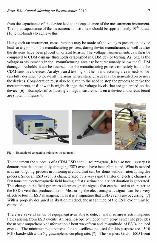
from the capacitance of the device lead to the capacitance of the measurement instrument. The input capacitance of the measurement instrument should be approximately 10-14 farads (10 femtofarads) to achieve this. Using such an instrument, measurements may be made of the voltages present on device leads at any point in the manufacturing process, during device manufacture, as well as after the devices have been placed on ci rcuit boards. The voltage measurements can then be compared to CDM damage thresholds established in CDM device testing. As long as the voltage m easurements in the manufacturing area a re ke pt reasonably below the C DM damage thresholds, it can be assumed that the manufacturing process can safely handle the CDM-sensitive d evices. An alysis an d testin g of t he m anufacturing area n eeds to be carefully designed to locate all the areas where static charge may be generated on or near the devices. Consideration must also be given to the need to stop the process to make the measurements, an d how th is might ch ange the voltage lev els t hat are gen erated on the device. [6] Examples of contacting voltage measurements on a device and circuit board are shown in Figure 4.
Fig. 4. Example of contacting voltmeter meaurement To doc ument the succes s of a CDM ESD cont rol program , it is also nec essary t o demonstrate that potentially damaging ESD events have been eliminated. What is needed is as an ongoing process m onitoring m ethod th at can be done without i nterrupting th e process. Since an ESD event is characterized by a very rapid transfer of electric charges, a fast transient electromagnetic field having a fast risetime and a short duration is generated. This change in the field generates electromagnetic signals that can be used to characterize the ESD e vent that produced them . Measuring the electromagnetic signa l can be a very effective tool in ESD management, as it is a signature that ESD events are occurring. [7] With a properly designed cal ibration method, t he magnitude of t he ESD event may be estimated. There are se veral ki nds of e quipment avai lable to detect and m easure e lectromagnetic fields arising from ESD events. An oscilloscope equipped with proper antennae provides the m ost c omprehensive i nformation a bout wa veform and m agnitude of ES D-induced events. The minimum requirements for an oscilloscope used for this purpose are a 50 0 MHz bandwidth and a 5 gigasamples/s sampling rate. [7] The simplest kind of ESD Event
Proc. ESA Annual Meeting on Electrostatics 2010 8
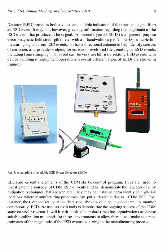
Detector (EED) provides both a visual and audible indication of the transient signal from an ESD event. It may not, however, give any information regarding the magnitude of the ESD e vent t hat pr oduced t he si gnal. A second t ype o f EE D i s a general-purpose electromagnetic field stren gth m eter with a bandwidth (u p to 2 GHz) su itable fo r measuring signals from ESD events. It has a directional antenna to help identify sources of emission, and provides outputs for emission l evels and the counting o f ESD events, including t ime st amping. This t ool can be ve ry use ful i n correlating ESD events with device handling or equipment operations. Several different types of EEDs are shown in Figure 5.
Fig.
EDs are es sential elem ents of the CDM sta tic con trol program. Th ey are used to
5. A sampling of available ESD Event Detectors (EED) Einvestigate t he source s of CDM ESD e vents a nd to demonstrate the success of a ny mitigation t echniques t hat a re applied. They may be i nstalled permanently i n high-risk locations where m anufacturing proce sses can put a device at risk to CDM ESD. For instance, the t est soc ket loc ation discussed above w ould be a g ood area to monitor continuously. EEDs are used as audit tools to demonstrate the ongoing success of the CDM static co ntrol p rogram. It will b e th e task of stan dards making organizations to devise suitable calibration m ethods for these ins truments to allow them to make accurate estimates of the magnitude of the ESD events occurring in the manufacturing process.
Proc. ESA Annual Meeting on Electrostatics 2010 9
VII. C ONCLUSION
tatic char ge control is a basic requirem ent in electronics manufacturing. Pre venting
iven t he co mplexity of t he device designs a nd t he va riety o f m anufacturing
REFERENCES [1] White Paper 2: A Case for Lower ing C CDM ESD Specifications and Requirements,
SCDM ES D damage re quires at tention t o device desi gn and a c omplete st atic co ntrol program. Such a pr ogram maintains de vice gr ound c ontact as much a s p ossible, uses static dissipative m aterials to re place i nsulators a nd to prevent da maging de vice discharges, eliminates metal-to-metal contact, and uses air ionization to neutralize charge on device packages and other process-essential insulators. Genvironments, device design for ESD control cannot, by itself, fully control CDM ESD problems. On ly a co mplete static co ntrol pr ogram i n all areas of manufacture a nd assembly can assure s uccessful, hi gh yiel d production of today’ s electronic devices. ANSI/ESD S20.20 and IEC 61340-5-1 st atic cont rol st andards provide guidance in the design and maintenance of a static control program. Fully solving the CDM ESD problem will require carefu l application of all th e el ements o f these programs, bu t verifying the operation of the elements of the static control is not sufficient. It will also be necessary to verify the results of t he st atic cont rol p rogram by de monstrating t hat t here are no potentially da maging voltages on t he devices t hemselves, a nd t hat t here a re n o ES D events occurring in the manufacturing area.
omponent Level Industry Device Council on E SD Target Levels, Apr il 2010. Available on the E SD Association website, http://www.esda.org/ [2] G. Rider, EFM – A Pernicious Threat To R eticles – Exposed, Future Fab In ternational, Is sue 25, April
f Electrical and Electronic Parts, Assemblies and Equipment (Excluding Electrically Initiated 2008, pp. 67-73 [3] Protection oExplosive Devices), ESD Association Standard ANSI/ESD S20.20, 2007, www.esda.org/ [4] Electrostatics P art 5- 1, Protection of E lectronic Devices from E lectrostatic P henomena – General Requirements, I nternational E lectrotechnical Co mmission ( IEC) Stan dard I EC 61340 -5-1, 2007- 2008, www.iec.ch [5] ESD Se nsitivity T esting – Cha rged Device Model – Component Level , E SD Association Standar d ANSI/ESD S5.3.1, 2009, www.esda.org/ [6] S. Halperin et al., Process Capability & Transitional Analysis, EOS/ESD Symposium 2008; pp 148-158
s [7] Kraz, V ., Measuring E lectromagnetic I nterference fro m ESD, Sem iconductor Equipment and MaterialInternational (SEMI) Standard SEMI E129-0706 - Guide to Controlling Electrostatic Charge in a Semiconductor Manufacturing Facility, Related Information 3, 2006, www.semi.org