euripides office 17, rue de l’amiral hamelin 75783 paris ... · 3 euripides sab – strategy...
TRANSCRIPT

EURIPIDES Office
17, rue de l’Amiral HAMELIN
75783 Paris cedex 16
FRANCE
September 2010 | version 1
EURIPIDES SAB - STRATEGY RESEARCH AGENDA
2 EURIPIDES SAB – Strategy Research Agenda
Version 1/ September 2010
INTRODUCTION AND EURIPIDES POSITION INSIDE EUREKA
EUREKA and its Information and Communications Technology (ICT) Clusters are making major
contributions to the future of ICT in Europe. CATRENE, CELTIC, EURIPIDES and ITEA 2 have clear views
on their roles in ensuring Europe maintains and increases its global leadership in a domain that is
crucial to the competitiveness of all major industrial sectors as well as to the wellbeing of European
citizens.
ICT and Smart System Integration will play a key role in the future prosperity of Europe. However,
while the global market is growing fast, research and development costs are rising even faster. As
few companies can support these costs alone, alliances are necessary, with similar public support in
Europe as is found in the rest of the world.
Europe needs micro/nanoelectronics and smart systems as a driving force and enabling technology,
with intensified efforts needed to fully exploit existing potential. While Europe is globally
competitive, it must continue to generate leading-edge technology at research centers of sufficient
size and critical mass, while at the same time stimulating the creativity and flexibility of smaller
organizations – particularly small and medium-sized enterprises (SMEs) – in creating new ideas and
applying them commercially.
Advanced System Integration and smart manufacturing processes for high-tech products in
numerous application fields
“ICT in the form of systems, software and services is responsible for innovations in most fields,” says
Jean Luc Maté, chairman of the EURIPIDES smart system integration cluster. “Hardware and software
integration is required in smart devices to deliver a complete system. However, while everyone
thinks Europe is the leader in systems design and architecture, they all envisage manufacture in the
Far East or other low cost region.”
Shared research and development strategies, accompanied by market success, will help break this
paradigm and allow people to think differently about high-tech, low-cost production in Europe. For
example, by using heterogeneous technology to improve integration and cut costs, overall
competitiveness can be improved dramatically. However, this requires innovative, imaginative ways
of technology development and manufacturing – also needing funding. In this context, EURIPIDES is a
forum for European product innovation, especially for SMEs, with the financing help of the different
member states of EUREKA. In contrast to Framework Programs of the EC, EURIPIDES (EUREKA) is a
bottom-up approach led by industry. In such an environment the total value chain from R&D to
production is considered.
It is necessary to make breakthroughs to maintain employment (and even create the innovative
stimulus to re-localize employment in Europe) by synchronizing research investment for both low
volume, high-tech strategic devices such as for medicine, aerospace and defense, and mass volume,
high-tech low-cost products for communications, multimedia, automotive, etc. This also includes the
improvement of existing products to fulfill new functionality needs and to extend their market
competitiveness. Both strategies meet the challenge that EURIPIDES faces for the next generation of
smart systems and their manufacturing processes.
3 EURIPIDES SAB – Strategy Research Agenda
Version 1/ September 2010
EURIPIDES mission
The EURIPIDES program is a modern, highly regarded tool to structure industrial projects and
reinforce the strength and position of SMEs and LEs on the international market of Smart Systems.
Main contributions to European electronic system and microsystem competitiveness are:
• Increase the R&D and manufacturing capabilities of European companies, with a specific
focus on SMEs in the growing global market of Smart Systems
• Development of advanced systems based on miniaturization, autonomy, reliability, or low
energy using techniques such as micro and nano technologies, interconnects, system-
oriented packaging and test
• Reducing time to market by organizing product value chains ,
• Support high volume, low cost solutions for smart systems and heterogeneous integration by
cooperation between high tech and low cost industry sectors
• Increase trans-national cooperation with the New European member States. Only high level
technology competencies of the whole community can guarantee the competitiveness of
Europe.
With more than 7,000 man-years of high-level research financed to date, EURIPIDES offers
unmatched capability in Europe to develop and deploy Integrated Smart Systems in such highly
diverse and complementary application fields as Automotive, Aeronautics, Medtech and Security.
With an average output of 170 M€ total cost of labeled projects per year, the results of the
EURIPIDES calls are encouraging.
The different technology domains covered by EURIPIDES members and projects are the following:
• Technologies for high reliability, high-density electronic modules
• Microsystems
• Technologies for smart cards
• Infrared sensors for medical applications
• THz imaging for security
• MEMS and MOEMS integration for all domains
• System in Packaging and chip stacking
• Optoelectronic and microwave on-chip
• LED systems and organic LED applications
• RFID integration
• Smart Wireless sensors and networks (ICs, passives, MEMS, antennas, ...)
• Ultra miniaturized modules for mobile communication
• Packaging for harsh environment
• Thermal management (materials, characterisation, simulation)
• Embedded systems: hardware and software co-design
• Reliability test and simulation, lifetime prediction
• Devices and systems for energy efficiency (e.g. for electric vehicle) ,
• Chemical sensing implementation ,
• Assembly and packaging of power systems
4 EURIPIDES SAB – Strategy Research Agenda
Version 1/ September 2010
EURIPIDES has a mission of near term development of new and improved products and technology
transfer, rather than a role of catalyst of mid to long term research. Consequently, EURIPIDES does
not compete with FP and platforms and is focused on linking research institutes and universities with
the industry and especially the SME’s to build up the value chain from R&D to production.
Europe has the advantage to have a rather efficient R&D infrastructure, but in order to link the
infrastructure to industry; EURIPIDES has a role to play as a facilitator for the support of innovative
projects relevant to industrial development. In addition, EURIPIDES strives for harmonization of
financing solutions through a strong effort of lobbying with public authorities to maintain and extend
the success of the program.
Through the long existence of EURIPIDES (previously Eurimus and Pidea) this mission has not
fundamentally changed and has proven to be highly appreciated by the industries using it. The
number of projects could be improved by building up more cross-border support.
The mission of EURIPIDES must be continuously focused on the bridging of national financing
authorities to facilitate technology transfer, irrespective of borders, for the benefit of the whole of
European industry. It will be shown that transnational cooperation between research institutes and
companies is the most effective way.
Structure of EURIPIDES inside EUREKA
As mentioned above, EURIPIDES is one of the EUREKA clusters devoted to ICT and Smart System
Integration.
EUREKA ‘Clusters’ are long-term, strategically significant industrial initiatives. They usually have a
large number of participants, and aim to develop generic technologies of key importance for
European competitiveness mainly in ICT, energy and more recently in the biotechnology sector.
Clusters bring together large companies, often competitors, along with SMEs, research institutes and
universities, sharing both the risk and benefits of innovation. They focus on developing and
commercially exploiting new technologies. Their goal is to ensure that Europe retains its leading
position in the world market.
Initiated by industry in close collaboration with national funding authorities, each Cluster has a
technological ‘roadmap’ defining the most important strategic domains. Specific goals are achieved
through scores of individual projects. A key asset of EUREKA is its flexibility: roadmaps and projects
are continuously adapted in response to the rapidly changing technological environment and market
demands.
Clusters aim to exploit the technologies developed through existing national and European programs
and play an important role in defining European standards and interoperability.
EURIPIDES promotes the development of new products, processes and services using or enabling the
use of integrated smart systems based on microtechnology.
5 EURIPIDES SAB – Strategy Research Agenda
Version 1/ September 2010
Large & Complex Systems
End-to-end solutions
Electronic System
Components
Optical components
Electronic packaging
& assembly
Micro/Nano
Electronics &
Software
Telecom
Application&S
ervicesMiddleware
Mobile&Home
Integration
Telecom NW
solutions
Security&Test
platforms
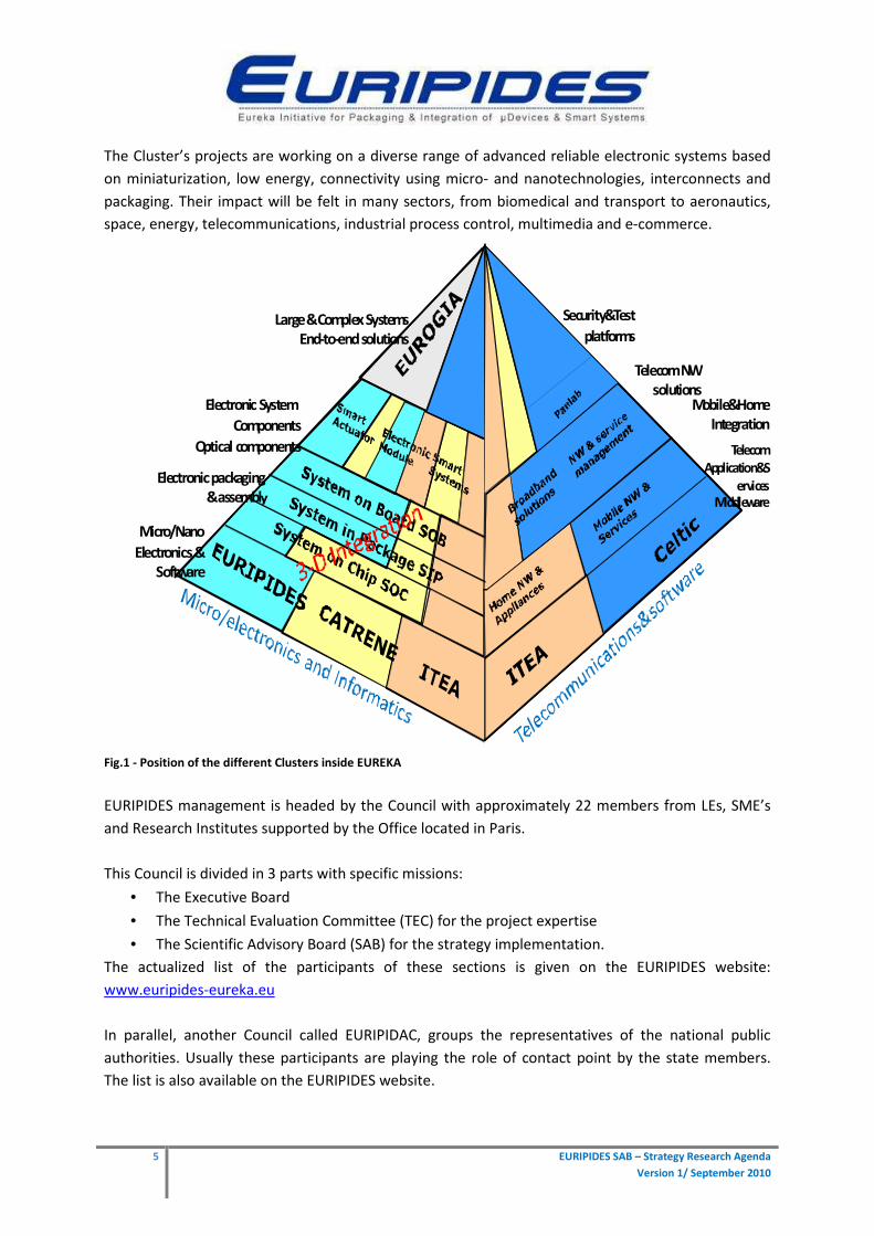
The Cluster’s projects are working on a diverse range of advanced reliable electronic systems based
on miniaturization, low energy, connectivity using micro- and nanotechnologies, interconnects and
packaging. Their impact will be felt in many sectors, from biomedical and transport to aeronautics,
space, energy, telecommunications, industrial process control, multimedia and e-commerce.
Fig.1 - Position of the different Clusters inside EUREKA
EURIPIDES management is headed by the Council with approximately 22 members from LEs, SME’s
and Research Institutes supported by the Office located in Paris.
This Council is divided in 3 parts with specific missions:
• The Executive Board
• The Technical Evaluation Committee (TEC) for the project expertise
• The Scientific Advisory Board (SAB) for the strategy implementation.
The actualized list of the participants of these sections is given on the EURIPIDES website:
www.euripides-eureka.eu
In parallel, another Council called EURIPIDAC, groups the representatives of the national public
authorities. Usually these participants are playing the role of contact point by the state members.
The list is also available on the EURIPIDES website.
6 EURIPIDES SAB – Strategy Research Agenda
Version 1/ September 2010
BUILDING PROJECTS AND FINANCING
EURIPIDES has been created with a clear industrial objective to support R&D activities in the area of
Smart Systems. The program management reflects this industrial involvement. The mainstream of
project partnerships will be built on small teams of industries and institutes teaming-up to achieve
advanced industrial results in the scope of EURIPIDES. Very large co-operative projects aiming at
achieving major breakthroughs and gathering larger consortia will also be encouraged. The ultimate
goal is to gain globally significant market shares for the European Heterogeneous system-based
industry with strong trans-European cooperation.
The rules for participation in a EUREKA project are the following:
• Main member: the country of the participant who submits the project or who is responsible
or who coordinates it must be a EUREKA member. The list of these countries is available on
the EUREKA web site: www.EUREKAnetwork.org
• Other members: they should come at least from another EUREKA member.
Associated countries can participate as any full EUREKA member with the only additional
requirement of a balanced European participation, involving at least two companies from
different EUREKA member countries.
• The non- EUREKA members or “Third Country”: they could participate as the third partner
only if at least 2 organizations from 2 EUREKA member countries are involved and they must
have secured funding (own private sources and/or combination own funding plus national
public co-funding) for participation in a project.
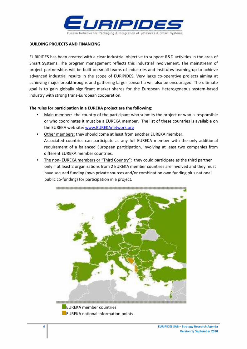
EUREKA member countries
EUREKA national information points
7 EURIPIDES SAB – Strategy Research Agenda
Version 1/ September 2010
Financing process
The EURIPIDES label allows a proposer from a EURIPIDES country to receive funding from its National
Public Authorities (NPAs) according to the national policy of this country. EURIPIDES proposers
should check the specific rules existing in the various countries before the submission of a PO
(Project Outline) to be sure that the project can be supported in every country.
Regular contacts are established between the EURIPIDES Council and the Public Authorities to
harmonize the access to funding. A “EURIPIDES Authority Council” (EURIPIDAC) is in place, gathering
members from the various EURIPIDES countries to facilitate the funding process from the beginning
of the proposal.
Project organization
Minimum 2 partners from EUREKA members: the main member should come from a EUREKA
country. Participants from associated countries or non-EUREKA members are submitted to special
rules. Please refer to the “EUREKA Project Form Guidelines”.
- One country’s share in a project should not exceed 75% of the total budget of the project (in
Euros).
- A Project Consortium Agreement (PCA) between the partners of the consortium should be
signed at the beginning of the project.
The most efficient method for building-up a consortium is to submit an “Expression of Interest” to
the EURIPIDES Office which can spread the information to the first level of members or on the
EURIPIDES website, depending on the level of confidentiality desired by the main contractor. If a
high level is requested, the Office can contact a limited number of persons able to find partners in
the right countries.
To submit a proposal, such consortium should constitute a European Consortium (EUREKA countries)
between businesses and/or research institutes.
The first step is to propose a Project Outline (PO). The PO is addressed to the EURIPIDES Office
before the closing date for PO submission. In the same time, each partner (or one per country)
contacts its national public authority to prepare the documents for project funding (Expression of
Interest, checking of the thematic priorities and existing program lines, clarification of the chances
for funding, etc.).
According to the EUREKA regulations, each country defines its own financing rules. Therefore some
discrepancies appear between the different EUREKA members in terms of:
• National Priorities in R/D topics
• ROI expectations
• Public/private financing ratio ; Industry/RTO public money distribution
In consequence, a primary contact with the National Authorities is highly recommended.
8 EURIPIDES SAB – Strategy Research Agenda
Version 1/ September 2010
If the project is selected by EURIPIDES Technical Evaluation Committee (TEC), the consortium is
invited to submit a Full Proposal Project (FPP).
In all cases, the excellence of project proposers and the quality of their co-operation will be the
major criteria for project selection by the EURIPIDES Council.
The project should be industry-driven with clear targets in terms of product development and/or
technology acquisition (know-how, patents, etc.). The economical impact is also a key issue.
The Call calendar for EURIPIDES, PO and FPP forms are available on EURIPIDES web site :
www.euripides-eureka.eu
BENEFITS FOR INDUSTRY AND MEMBER COUNTRIES
As mentioned in the mission, EURIPIDES is more focused in the development of new and improved
products and technology transfer than as catalyst of future research. EURIPIDES is devoted to linking
research institutes with the industry and especially the SME’s to fill the gap between R&D and
production.
Due to its extensive network EURIPIDES is the organization which can provide partners covering the
total value chain from research, design, development, prototyping, small scale production for market
launch and even large scale production. Some companies specialized in product dissemination can
also be added.
Specific benefits for industrial EURIPIDES members are:
• Introduction in the European R&D network (Road mapping, Know How, Intellectual Property,
etc.)
• Funding of product developments (from EUREKA member states)
• Establishment as a supplier
• Complete own value chain
• Prototyping and pre-production for market evaluation
• Access to volume production facilities
• Contact with distribution networks
The benefit for the EUREKA member states participating in EURIPIDES includes active support for
industry, including both SMEs and LEs, to identify and interact with partners, subcontractors, product
distributors, etc. inside Europe and keep the know-how on the continent.
Specific advantages for the member states are:
• Maintain a leading position in high tech system integration
• Strengthen industrial networks, preserving and creating jobs,
• Expand reach of national companies to international business
• Connect start-ups to complete value chains
• Achieve national and international recognition for high tech performance
9 EURIPIDES SAB – Strategy Research Agenda
Version 1/ September 2010
While not all countries support EURIPIDES projects equally, some regional sources of financing can
also be engaged as alternative or complementary financing. EURIPIDES remains committed to
bringing together the strongest consortiums for the projects within the EUREKA states, regardless of
national borders. The market success of the participating companies and the growth of the European
high tech sector will provide the validation to the national authorities that transnational cooperation
between research institutes and companies is the most effective way.
SUCCESS STORIES
Some examples of successful projects can be directly attributed to the EURIPIDES cluster. New
technologies or new products are the outcomes and their benefits are visible in our everyday lives.
EURIPIDES success stories cover a large range of applications including medical, communication,
automotive, health, safety, security,etc.
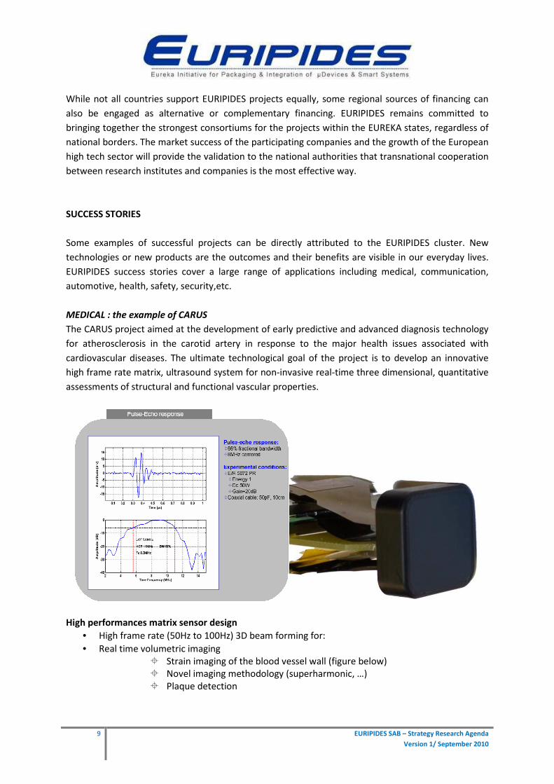
MEDICAL : the example of CARUS
The CARUS project aimed at the development of early predictive and advanced diagnosis technology
for atherosclerosis in the carotid artery in response to the major health issues associated with
cardiovascular diseases. The ultimate technological goal of the project is to develop an innovative
high frame rate matrix, ultrasound system for non-invasive real-time three dimensional, quantitative
assessments of structural and functional vascular properties.
High performances matrix sensor design
• High frame rate (50Hz to 100Hz) 3D beam forming for:
• Real time volumetric imaging
� Strain imaging of the blood vessel wall (figure below)
� Novel imaging methodology (superharmonic, …)
� Plaque detection
10 EURIPIDES SAB – Strategy Research Agenda
Version 1/ September 2010
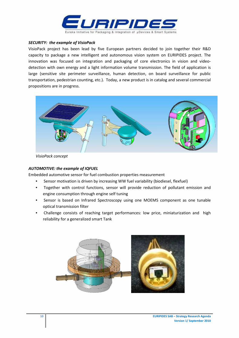
SECURITY: the example of VisioPack
VisioPack project has been lead by five European partners decided to join together their R&D
capacity to package a new intelligent and autonomous vision system on EURIPIDES project. The
innovation was focused on integration and packaging of core electronics in vision and video-
detection with own energy and a light information volume transmission. The field of application is
large (sensitive site perimeter surveillance, human detection, on board surveillance for public
transportation, pedestrian counting, etc.). Today, a new product is in catalog and several commercial
propositions are in progress.
VisioPack concept
AUTOMOTIVE: the example of IQFUEL
Embedded automotive sensor for fuel combustion properties measurement
• Sensor motivation is driven by increasing WW fuel variability (biodiesel, flexfuel)
• Together with control functions, sensor will provide reduction of pollutant emission and
engine consumption through engine self tuning
• Sensor is based on Infrared Spectroscopy using one MOEMS component as one tunable
optical transmission filter
• Challenge consists of reaching target performances: low price, miniaturization and high
reliability for a generalized smart Tank
11 EURIPIDES SAB – Strategy Research Agenda
Version 1/ September 2010
Courtesy of 3D PLUS
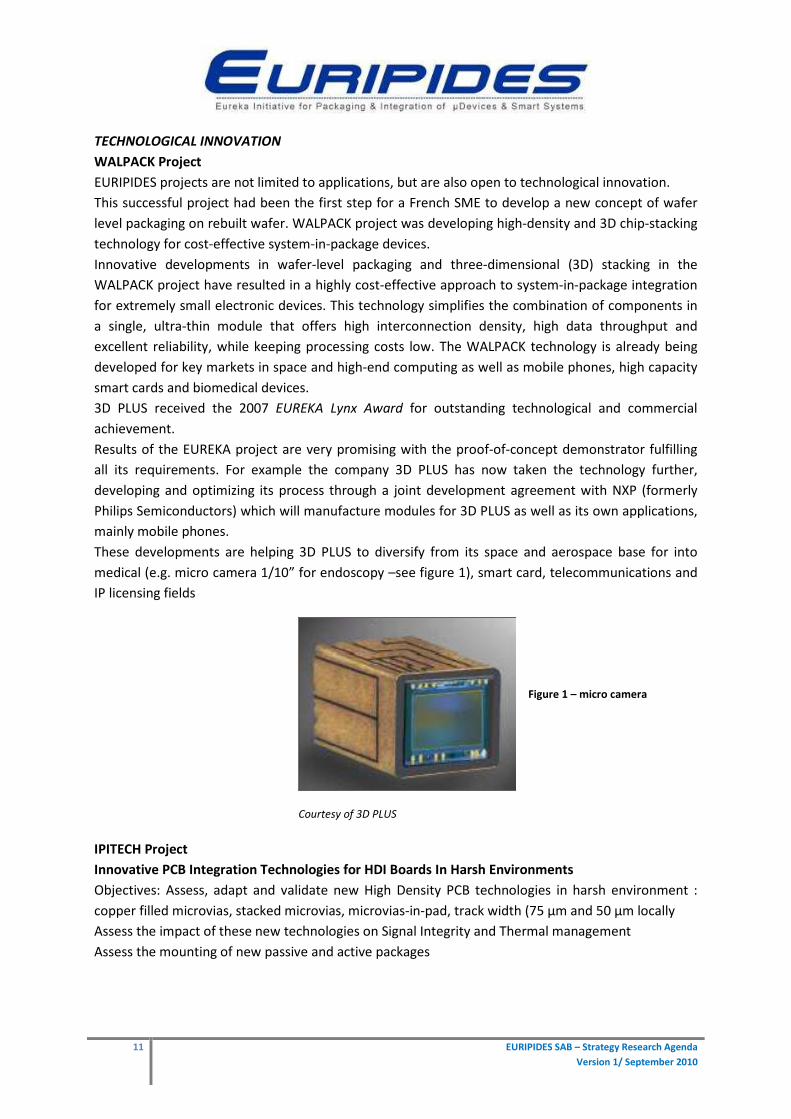
TECHNOLOGICAL INNOVATION
WALPACK Project
EURIPIDES projects are not limited to applications, but are also open to technological innovation.
This successful project had been the first step for a French SME to develop a new concept of wafer
level packaging on rebuilt wafer. WALPACK project was developing high-density and 3D chip-stacking
technology for cost-effective system-in-package devices.
Innovative developments in wafer-level packaging and three-dimensional (3D) stacking in the
WALPACK project have resulted in a highly cost-effective approach to system-in-package integration
for extremely small electronic devices. This technology simplifies the combination of components in
a single, ultra-thin module that offers high interconnection density, high data throughput and
excellent reliability, while keeping processing costs low. The WALPACK technology is already being
developed for key markets in space and high-end computing as well as mobile phones, high capacity
smart cards and biomedical devices.
3D PLUS received the 2007 EUREKA Lynx Award for outstanding technological and commercial
achievement.
Results of the EUREKA project are very promising with the proof-of-concept demonstrator fulfilling
all its requirements. For example the company 3D PLUS has now taken the technology further,
developing and optimizing its process through a joint development agreement with NXP (formerly
Philips Semiconductors) which will manufacture modules for 3D PLUS as well as its own applications,
mainly mobile phones.
These developments are helping 3D PLUS to diversify from its space and aerospace base for into
medical (e.g. micro camera 1/10” for endoscopy –see figure 1), smart card, telecommunications and
IP licensing fields
Figure 1 – micro camera
IPITECH Project
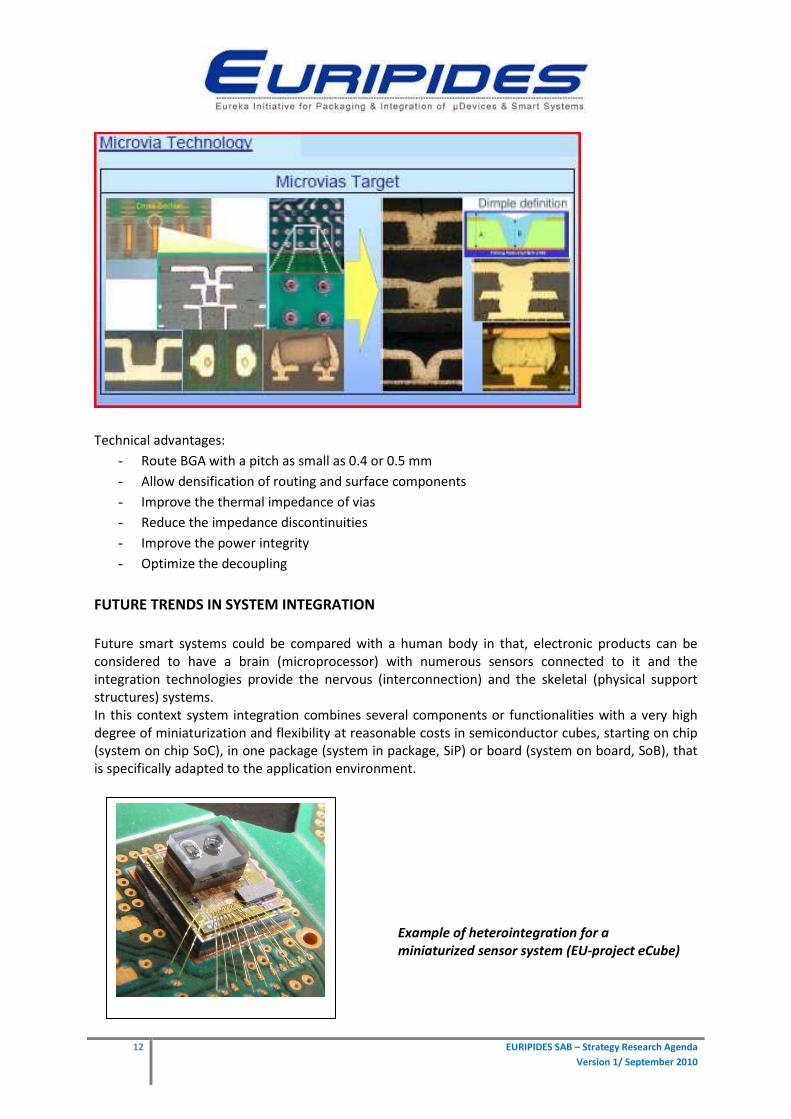
Innovative PCB Integration Technologies for HDI Boards In Harsh Environments
Objectives: Assess, adapt and validate new High Density PCB technologies in harsh environment :
copper filled microvias, stacked microvias, microvias-in-pad, track width (75 µm and 50 µm locally
Assess the impact of these new technologies on Signal Integrity and Thermal management
Assess the mounting of new passive and active packages
12 EURIPIDES SAB – Strategy Research Agenda
Version 1/ September 2010
Technical advantages:
- Route BGA with a pitch as small as 0.4 or 0.5 mm
- Allow densification of routing and surface components
- Improve the thermal impedance of vias
- Reduce the impedance discontinuities
- Improve the power integrity
- Optimize the decoupling
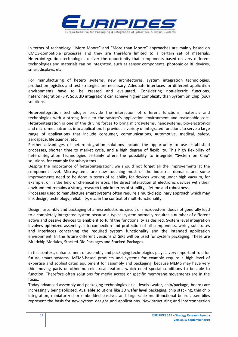
FUTURE TRENDS IN SYSTEM INTEGRATION
Future smart systems could be compared with a human body in that, electronic products can be
considered to have a brain (microprocessor) with numerous sensors connected to it and the
integration technologies provide the nervous (interconnection) and the skeletal (physical support
structures) systems.
In this context system integration combines several components or functionalities with a very high
degree of miniaturization and flexibility at reasonable costs in semiconductor cubes, starting on chip
(system on chip SoC), in one package (system in package, SiP) or board (system on board, SoB), that
is specifically adapted to the application environment.
Example of heterointegration for a
miniaturized sensor system (EU-project eCube)
13 EURIPIDES SAB – Strategy Research Agenda
Version 1/ September 2010
In terms of technology, “More Moore” and “More than Moore” approaches are mainly based on
CMOS-compatible processes and they are therefore limited to a certain set of materials.
Heterointegration technologies deliver the opportunity that components based on very different
technologies and materials can be integrated, such as sensor components, photonic or RF devices,
smart displays, etc.
For manufacturing of hetero systems, new architectures, system integration technologies,
production logistics and test strategies are necessary. Adequate interfaces for different application
environments have to be created and evaluated. Considering non-electric functions,
heterointegration (SiP, SoB, 3D integration) can achieve higher complexity than System on Chip (SoC)
solutions.
Heterointegration technologies provide the interaction of different functions, materials and
technologies with a strong focus to the system’s application environment and reasonable cost.
Heterointegration is one of the driving forces to bring microsystems, nanosystems, bio-electronics
and micro-mechatronics into application. It provides a variety of integrated functions to serve a large
range of applications that include consumer, communications, automotive, medical, safety,
aerospace, life science, etc.
Further advantages of heterointegration solutions include the opportunity to use established
processes, shorter time to market cycle, and a high degree of flexibility. This high flexibility of
heterointegration technologies certainly offers the possibility to integrate “System on Chip”
solutions, for example for subsystems.
Despite the importance of heterointegration, we should not forget all the improvements at the
component level. Microsystems are now touching most of the industrial domains and some
improvements need to be done in terms of reliability for devices working under high vacuum, for
example, or in the field of chemical sensors. The direct interaction of electronic devices with their
environment remains a strong research topic in terms of stability, lifetime and robustness.
Processes used to manufacture smart systems often require a multi-disciplinary approach which may
link design, technology, reliability, etc. in the context of multi-functionality.
Design, assembly and packaging of a microelectronic circuit or microsystem does not generally lead
to a completely integrated system because a typical system normally requires a number of different
active and passive devices to enable it to fulfil the functionality as desired. System level integration
involves optimized assembly, interconnection and protection of all components, wiring substrates
and interfaces concerning the required system functionality and the intended application
environment. In the future different versions of SiPs will be used for system packaging. These are
Multichip Modules, Stacked-Die Packages and Stacked-Packages.
In this context, enhancement of assembly and packaging technologies plays a very important role for
future smart systems. MEMS-based products and systems for example require a high level of
expertise and sophisticated equipment for assembly and packaging, because MEMS may have very
thin moving parts or other non-electrical features which need special conditions to be able to
function. Therefore often solutions for media access or specific membrane movements are in the
focus.
Today advanced assembly and packaging technologies at all levels (wafer, chip/package, board) are
increasingly being solicited. Available solutions like 3D wafer level packaging, chip stacking, thin chip
integration, miniaturized or embedded passives and large-scale multifunctional board assemblies
represent the basis for new system designs and applications. New structuring and interconnection
14 EURIPIDES SAB – Strategy Research Agenda
Version 1/ September 2010
methods (e.g. nano-interconnects) lead to very small system sizes and provide the opportunity for
functionality oriented system assemblies. This is a new challenge for interconnection and packaging:
to switch from technology oriented packaging to system oriented packaging.
The following needs have to be in focus to extend advanced assembly and packaging in the future:
• low cost interconnection technologies (high density multilevel wire bonding, fine pitch flip
chip, thin interconnects, fine pitch TSVs)
• interconnects and packages for high temperature and harsh environment
• low temperature assembly technologies
• low cost high speed assembly
• special functionality oriented mould compounds (e.g. with nanoparticles)
• improved materials functionality, such as new electrical, optical, thermal properties (e.g. by
Carbon NanoTubes)
• 3D compatible actives and passives (e.g. nano structured materials for high k capacitors, low
k inductors, interposer, thin chips)
• high accuracy positioning and self positioning/assembly technologies of die, devices,
components, interconnects, etc.
Because of their strong relevance, 3D wafer-level packaging on the one hand side and board level
system packaging on the other side will dominate future product manufacturing.
EURIPIDES community is committed to help European industries to absorb such new
technologies to create a wealth of new products and to keep our innovation forces to the
highest level.
CONTACT THE EURIPIDES OFFICE FOR FURTHER INFORMATION :
17, rue de l’Amiral HAMELIN
75783 Paris cedex 16
FRANCE
Tel : +33 1 45 05 70 49
Fax: +33 1 45 05 70 37