etsi en 300 394-1 v3.3 · etsi 2 etsi en 300 394-1 v3.3.1 (2015-04) reference ren/tcce-03233...
TRANSCRIPT
ETSI EN 300 394-1 V3.3.1 (2015-04)
Terrestrial Trunked Radio (TETRA); Conformance testing specification;
Part 1: Radio
EUROPEAN STANDARD
ETSI
ETSI EN 300 394-1 V3.3.1 (2015-04)2
Reference REN/TCCE-03233
Keywords DMO, testing, TETRA, V+D
ETSI
650 Route des Lucioles F-06921 Sophia Antipolis Cedex - FRANCE
Tel.: +33 4 92 94 42 00 Fax: +33 4 93 65 47 16
Siret N° 348 623 562 00017 - NAF 742 C
Association à but non lucratif enregistrée à la Sous-Préfecture de Grasse (06) N° 7803/88
Important notice
The present document can be downloaded from: http://www.etsi.org/standards-search
The present document may be made available in electronic versions and/or in print. The content of any electronic and/or print versions of the present document shall not be modified without the prior written authorization of ETSI. In case of any
existing or perceived difference in contents between such versions and/or in print, the only prevailing document is the print of the Portable Document Format (PDF) version kept on a specific network drive within ETSI Secretariat.
Users of the present document should be aware that the document may be subject to revision or change of status. Information on the current status of this and other ETSI documents is available at
http://portal.etsi.org/tb/status/status.asp
If you find errors in the present document, please send your comment to one of the following services: https://portal.etsi.org/People/CommiteeSupportStaff.aspx
Copyright Notification
No part may be reproduced or utilized in any form or by any means, electronic or mechanical, including photocopying and microfilm except as authorized by written permission of ETSI.
The content of the PDF version shall not be modified without the written authorization of ETSI. The copyright and the foregoing restriction extend to reproduction in all media.
© European Telecommunications Standards Institute 2015.
All rights reserved.
DECTTM, PLUGTESTSTM, UMTSTM and the ETSI logo are Trade Marks of ETSI registered for the benefit of its Members. 3GPPTM and LTE™ are Trade Marks of ETSI registered for the benefit of its Members and
of the 3GPP Organizational Partners. GSM® and the GSM logo are Trade Marks registered and owned by the GSM Association.
ETSI
ETSI EN 300 394-1 V3.3.1 (2015-04)3
Contents Intellectual Property Rights ...................................................................................................................... 10
Foreword ................................................................................................................................................... 10
Modal verbs terminology .......................................................................................................................... 10
Introduction .............................................................................................................................................. 10
1 Scope .............................................................................................................................................. 11
2 References ...................................................................................................................................... 11
2.1 Normative references .............................................................................................................................. 11
2.2 Informative references ............................................................................................................................. 12
3 Definitions, symbols and abbreviations ......................................................................................... 12
3.1 Definitions ............................................................................................................................................... 12
3.2 Symbols ................................................................................................................................................... 12
3.3 Abbreviations .......................................................................................................................................... 13
4 General ........................................................................................................................................... 13
4.1 Presentation of equipment for testing purposes ....................................................................................... 13
4.1.1 Facilities and information required for testing ................................................................................... 14
4.1.2 Choice of radio frequency channels to be tested ................................................................................ 14
4.1.3 Interpretation of the measurement results .......................................................................................... 15
4.2 Mechanical and electrical design ............................................................................................................. 15
4.2.1 General ............................................................................................................................................... 15
4.2.2 Controls ............................................................................................................................................. 15
4.2.3 Marking ............................................................................................................................................. 15
5 Radio test configuration, test signals and test modes ..................................................................... 15
5.1 General functional radio test configuration ............................................................................................. 15
5.2 Radio test modes ..................................................................................................................................... 16
5.2.1 Test receive mode .............................................................................................................................. 16
5.2.1.1 MS test receive mode for phase modulation ................................................................................ 16
5.2.1.2 BS test receive mode for phase modulation ................................................................................. 17
5.2.1.3 MS test receive mode for QAM (where supported) ..................................................................... 17
5.2.1.4 BS test receive mode for QAM (where supported) ...................................................................... 18
5.2.2 Test transmit mode............................................................................................................................. 19
5.2.2.1 MS testing for phase modulation ................................................................................................. 19
5.2.2.2 Void.............................................................................................................................................. 19
5.2.2.3 BS testing for phase modulation .................................................................................................. 19
5.2.2.4 MS testing for QAM (where supported) ...................................................................................... 19
5.2.2.5 BS testing for QAM (where supported) ....................................................................................... 20
5.3 Radio test signals ..................................................................................................................................... 21
5.3.1 General ............................................................................................................................................... 21
5.3.2 Test signal T1 (TETRA wanted signal, phase modulation) ............................................................... 21
5.3.2.1 MS testing .................................................................................................................................... 21
5.3.2.2 BS testing ..................................................................................................................................... 22
5.3.2.3 Void.............................................................................................................................................. 23
5.3.2.4 Void.............................................................................................................................................. 23
5.3.3 Test signal T2 (TETRA interferer) .................................................................................................... 23
5.3.4 Test signal T3 (unmodulated interferer) ............................................................................................ 23
5.3.5 Test signal T4 (TETRA wanted signal, QAM) .................................................................................. 23
5.3.5.1 MS testing .................................................................................................................................... 23
5.3.5.1.1 Use of synchronization burst in frame 18 when testing CA MSs ........................................... 25
5.3.5.1.1a Use of frequency correction burst in frame 18 when testing DA MSs ................................... 26
5.3.5.2 BS testing ..................................................................................................................................... 28
6 Test conditions ............................................................................................................................... 29
6.1 General .................................................................................................................................................... 29
6.2 Power sources and ambient conditions .................................................................................................... 29
6.2.1 Normal test conditions ....................................................................................................................... 29
ETSI
ETSI EN 300 394-1 V3.3.1 (2015-04)4
6.2.2 Extreme test conditions ...................................................................................................................... 30
6.3 Procedure for tests at extreme temperatures ............................................................................................ 31
6.3.1 Equipment designed for continuous operation ................................................................................... 31
6.3.2 Equipment designed for intermittent operation.................................................................................. 31
7 Technical characteristics ................................................................................................................ 31
7.1 Transmitter parameter definitions and limits ........................................................................................... 31
7.1.1 Transmitter output power ................................................................................................................... 31
7.1.1.1 Definition ..................................................................................................................................... 31
7.1.1.2 Limit values for phase modulation and QAM .............................................................................. 32
7.1.2 Unwanted output power in non-active transmit state ......................................................................... 32
7.1.2.1 Definition ..................................................................................................................................... 32
7.1.2.2 Limit values.................................................................................................................................. 32
7.1.3 Adjacent channel power due to modulation ....................................................................................... 32
7.1.3.1 Definition ..................................................................................................................................... 32
7.1.3.2 Limit values for phase modulation ............................................................................................... 32
7.1.3.3 Limit values for QAM .................................................................................................................. 33
7.1.4 Adjacent channel power due to switching transients ......................................................................... 34
7.1.4.1 Definition ..................................................................................................................................... 34
7.1.4.2 Limit values for phase modulation ............................................................................................... 34
7.1.4.3 Limit values for QAM .................................................................................................................. 34
7.1.5 Unwanted emissions far from the carrier ........................................................................................... 34
7.1.5.1 Definition ..................................................................................................................................... 34
7.1.5.2 Limit values for phase modulation ............................................................................................... 35
7.1.5.3 Limit values for QAM .................................................................................................................. 35
7.1.6 Unwanted radiated emissions ............................................................................................................ 37
7.1.6.1 Definition ..................................................................................................................................... 37
7.1.6.2 Limit values.................................................................................................................................. 37
7.1.7 Unwanted emissions during the BLCH/CLCH (linearization) .......................................................... 37
7.1.7.1 Definition ..................................................................................................................................... 37
7.1.7.2 Limit values for phase modulation ............................................................................................... 37
7.1.7.3 Limit values for QAM .................................................................................................................. 37
7.1.8 Transmitter intermodulation attenuation ............................................................................................ 37
7.1.8.1 Definition ..................................................................................................................................... 37
7.1.8.2 Limit values for phase modulation and QAM .............................................................................. 38
7.1.8.2.1 MS Limit values ..................................................................................................................... 38
7.1.8.2.2 Limit values for single BS transmitter .................................................................................... 38
7.1.8.2.3 Limit values for intra BS intermodulation .............................................................................. 38
7.2 Receiver parameter definitions and limits ............................................................................................... 38
7.2.1 General ............................................................................................................................................... 38
7.2.2 Nominal error rates ............................................................................................................................ 39
7.2.2.1 Definition ..................................................................................................................................... 39
7.2.2.2 Limit values for phase modulation ............................................................................................... 39
7.2.2.3 Limit values for QAM .................................................................................................................. 39
7.2.3 Reference sensitivity performance ..................................................................................................... 39
7.2.3.1 Definition ..................................................................................................................................... 39
7.2.3.2 Limit values for phase modulation ............................................................................................... 39
7.2.3.3 Limit values for QAM .................................................................................................................. 40
7.2.4 Reference interference performance .................................................................................................. 41
7.2.4.1 Definition ..................................................................................................................................... 41
7.2.4.2 Limit values for phase modulation ............................................................................................... 42
7.2.4.3 Limit values for QAM .................................................................................................................. 42
7.2.4.3.1 Adjacent channel interference ................................................................................................ 42
7.2.4.3.2 Co-channel interference .......................................................................................................... 43
7.2.5 Blocking characteristics ..................................................................................................................... 43
7.2.5.1 Definition ..................................................................................................................................... 43
7.2.5.2 Limit values for phase modulation ............................................................................................... 43
7.2.5.3 Limit values for QAM .................................................................................................................. 44
7.2.6 Spurious response rejection ............................................................................................................... 44
7.2.6.1 Definition ..................................................................................................................................... 44
7.2.6.2 Limit values for phase modulation ............................................................................................... 45
7.2.6.3 Limit values for QAM .................................................................................................................. 45
ETSI
ETSI EN 300 394-1 V3.3.1 (2015-04)5
7.2.7 Intermodulation response rejection .................................................................................................... 45
7.2.7.1 Definition ..................................................................................................................................... 45
7.2.7.2 Limit values.................................................................................................................................. 45
7.2.8 Unwanted conducted emissions ......................................................................................................... 46
7.2.8.1 Definition ..................................................................................................................................... 46
7.2.8.2 Limit values.................................................................................................................................. 46
7.2.9 Unwanted radiated emissions ............................................................................................................ 46
7.2.9.1 Definition ..................................................................................................................................... 46
7.2.9.2 Limit values.................................................................................................................................. 46
7.3 Transmitter/receiver parameter definitions and limits ............................................................................. 46
7.3.1 Modulation accuracy.......................................................................................................................... 46
7.3.1.1 Definition ..................................................................................................................................... 46
7.3.1.2 Limit values for phase modulation ............................................................................................... 47
7.3.1.3 Limit values for QAM .................................................................................................................. 47
7.3.2 Carrier frequency accuracy ................................................................................................................ 47
7.3.2.1 Definition ..................................................................................................................................... 47
7.3.2.2 Limit values.................................................................................................................................. 47
7.3.3 MS receiver performance for synchronization burst acquisition ....................................................... 47
7.3.3.1 Definition for phase modulation .................................................................................................. 47
7.3.3.2 Limit values for phase modulation ............................................................................................... 47
7.3.3.3 Definition for QAM modulation .................................................................................................. 48
7.3.3.4 Limit values for QAM modulation ............................................................................................... 48
7.3.4 MS Frame alignment performance .................................................................................................... 48
7.3.4.1 Definition ..................................................................................................................................... 48
7.3.4.2 Limit values.................................................................................................................................. 48
7.3.5 MS link control .................................................................................................................................. 48
7.3.5.1 Definition ..................................................................................................................................... 48
7.3.5.2 Limit values.................................................................................................................................. 48
8 Methods of measurement for transmitter parameters ..................................................................... 49
8.1 Transmitter output power ........................................................................................................................ 49
8.1.1 Transmitter output power for phase modulation ................................................................................ 49
8.1.1.1 MS transmitter output power for phase modulation ..................................................................... 49
8.1.1.2 BS transmitter output power for phase modulation ...................................................................... 50
8.1.2 Transmitter output power for QAM ................................................................................................... 51
8.1.2.1 MS transmitter output power for QAM ........................................................................................ 51
8.1.2.2 BS transmitter output power for QAM......................................................................................... 52
8.2 Unwanted output power in non active transmit state ............................................................................... 52
8.3 Adjacent channel power due to modulation ............................................................................................ 52
8.4 Adjacent channel power due to switching transients ............................................................................... 53
8.5 Unwanted emissions far from the carrier ................................................................................................ 53
8.6 Unwanted radiated emissions .................................................................................................................. 55
8.7 Unwanted emissions during the BLCH/CLCH and BLCH-Q/CLCH-Q (linearization) ......................... 55
8.7.1 MS unwanted emissions during the CLCH (linearization) ................................................................ 55
8.7.2 BS unwanted emissions during the BLCH (linearization) ................................................................. 56
8.7.3 MS unwanted emissions during the CLCH-Q (linearization) ............................................................ 56
8.7.4 BS unwanted emissions during the BLCH-Q (linearization) ............................................................. 56
8.8 Transmitter intermodulation attenuation ................................................................................................. 57
8.8.1 MS Transmitter intermodulation attenuation ..................................................................................... 57
8.8.2 BS Transmitter intermodulation attenuation ...................................................................................... 57
8.8.3 Intra BS transmitter intermodulation attenuation ............................................................................... 57
9 Methods of measurement for receiver parameters ......................................................................... 57
9.1 General .................................................................................................................................................... 57
9.2 Nominal error rates for phase modulation ............................................................................................... 57
9.2.1 MS nominal error rate ........................................................................................................................ 57
9.2.2 BS nominal error rate ......................................................................................................................... 58
9.3 Reference sensitivity performance .......................................................................................................... 58
9.3.1 MS reference sensitivity performance for phase modulation ............................................................. 58
9.3.2 BS reference sensitivity performance for phase modulation ............................................................. 58
9.3.3 MS reference sensitivity performance for QAM ............................................................................... 59
9.3.4 BS reference sensitivity performance for QAM ................................................................................ 59
ETSI
ETSI EN 300 394-1 V3.3.1 (2015-04)6
9.3.5 PUEM performance ........................................................................................................................... 59
9.4 Reference interference performance ........................................................................................................ 59
9.4.1 MS reference interference performance for phase modulation .......................................................... 59
9.4.2 BS reference interference performance for phase modulation ........................................................... 60
9.4.3 MS reference interference performance for QAM ............................................................................. 60
9.4.4 BS reference interference performance for QAM .............................................................................. 60
9.5 Blocking characteristics .......................................................................................................................... 61
9.5.1 MS blocking for phase modulation .................................................................................................... 61
9.5.2 BS blocking for phase modulation ..................................................................................................... 61
9.5.3 MS blocking for QAM ....................................................................................................................... 61
9.5.4 BS blocking for QAM........................................................................................................................ 62
9.6 Spurious response rejection ..................................................................................................................... 62
9.6.1 Phase Modulation .............................................................................................................................. 62
9.6.2 QAM .................................................................................................................................................. 62
9.7 Intermodulation response rejection ......................................................................................................... 62
9.7.1 MS intermodulation response rejection for phase modulation ........................................................... 62
9.7.2 BS intermodulation response rejection for phase modulation ........................................................... 63
9.7.3 MS intermodulation response rejection for QAM ............................................................................. 63
9.7.4 BS intermodulation response rejection for QAM .............................................................................. 63
9.8 Unwanted emissions ................................................................................................................................ 64
9.9 Unwanted radiated emissions .................................................................................................................. 64
10 Methods of measurement for transmitter/receiver parameters ....................................................... 64
10.1 Modulation accuracy ............................................................................................................................... 64
10.1.1 MS modulation accuracy for phase modulation................................................................................. 65
10.1.2 BS modulation accuracy for phase modulation ................................................................................. 65
10.1.3 Vector error magnitude at symbol time for phase modulation ........................................................... 65
10.1.4 MS modulation accuracy for QAM ................................................................................................... 65
10.1.5 BS modulation accuracy for QAM .................................................................................................... 65
10.1.6 Vector error magnitude at symbol time for QAM ............................................................................. 66
10.2 Carrier frequency accuracy...................................................................................................................... 66
10.2.1 MS carrier frequency accuracy for phase modulation ....................................................................... 66
10.2.2 BS carrier frequency accuracy for phase modulation ........................................................................ 67
10.2.3 MS carrier frequency accuracy for QAM .......................................................................................... 67
10.2.4 BS carrier frequency accuracy for QAM ........................................................................................... 68
10.3 MS receiver performance for synchronization acquisition ...................................................................... 68
10.3.1 CA MS receiver performance for synchronization burst acquisition ................................................. 68
10.3.2 DA MS receiver performance for frequency correction burst acquisition ......................................... 69
10.4 MS Frame alignment performance .......................................................................................................... 69
10.5 MS link control ........................................................................................................................................ 69
11 Measurement uncertainty ............................................................................................................... 70
11.1 Transmitter .............................................................................................................................................. 71
11.2 Receiver ................................................................................................................................................... 74
11.3 Transmitter/receiver parameter definitions and limits ............................................................................. 76
11.4 Interpretation of measurement results ..................................................................................................... 77
Annex A (normative): TETRA receiver testing ................................................................................... 78
A.1 Frequencies of spurious response ................................................................................................... 78
A.2 Test cases and test conditions for BS and MS receivers ................................................................ 78
A.3 Test signal T1/T4, content of BSCH, BSCH-Q/T, BNCH/T and BNCH-Q/T ............................. 103
Annex B (normative): Radio test system functions............................................................................ 109
B.1 Test transmitter and receiver ........................................................................................................ 109
B.1.1 General .................................................................................................................................................. 109
B.1.2 Sampling system ................................................................................................................................... 109
B.1.2.1 General ............................................................................................................................................. 109
B.1.2.2 TETRA filter .................................................................................................................................... 109
B.1.2.3 Adjacent channel power measurements ........................................................................................... 110
B.1.2.4 Modulation accuracy measurements ................................................................................................ 110
ETSI
ETSI EN 300 394-1 V3.3.1 (2015-04)7
B.1.2.5 Measurement of unwanted output power in the non-active transmit state ....................................... 110
B.1.3 Spectrum analyser ................................................................................................................................. 110
B.1.4 Error rate tester ...................................................................................................................................... 110
B.1.5 Test signal requirements ........................................................................................................................ 111
B.1.5.1 On channel test signal T1 ................................................................................................................. 111
B.1.5.2 Interfering test signal T2 .................................................................................................................. 111
B.1.5.2.1 Phase Modulated ........................................................................................................................ 111
B.1.5.2.2 QAM Modulated ........................................................................................................................ 111
B.1.5.3 Interfering test signal T3 .................................................................................................................. 111
B.1.5.4 On channel test signal T4 ................................................................................................................. 112
B.1.6 Propagation simulators .......................................................................................................................... 112
B.1.7 Timing measurement unit ...................................................................................................................... 112
B.1.8 Passive test system components ............................................................................................................ 112
B.1.9 Test system controller ........................................................................................................................... 112
Annex C (normative): TETRA Test Connector Interface (TTCI) ................................................... 113
C.1 General ......................................................................................................................................... 113
C.2 Formal aspects .............................................................................................................................. 113
C.3 TTCI, layer 1 ................................................................................................................................ 114
C.3.1 Mechanical and electrical characteristics .............................................................................................. 114
C.3.2 Transmission and reception characteristics ........................................................................................... 114
C.4 TTCI, Layer 2 ............................................................................................................................... 114
C.4.1 General structure ................................................................................................................................... 114
C.4.2 Frame structure ...................................................................................................................................... 114
C.4.3 Flow of I-frames on layer 2 ................................................................................................................... 115
C.4.3.1 Transmission of frames .................................................................................................................... 115
C.4.3.2 Reception of frames ......................................................................................................................... 115
C.4.3.3 Parameters on layer 2 ....................................................................................................................... 116
C.5 TTCI, Layer 3 ............................................................................................................................... 116
C.5.1 Message structure .................................................................................................................................. 116
C.5.2 Definitions of the messages ................................................................................................................... 116
C.5.2.1 DATO .............................................................................................................................................. 116
C.5.2.1.1 Test equipment error handling ................................................................................................... 118
C.5.2.2 Bi-directional operation of the TTCI ............................................................................................... 118
C.5.2.3 Codec conformance testing .............................................................................................................. 119
C.5.2.4 ST indicator ..................................................................................................................................... 119
C.6 Control of MS/BS ......................................................................................................................... 119
C.6.1 Manual intervention of MS/BS ............................................................................................................. 119
C.6.2 Bi-directional operation of the test interface ......................................................................................... 119
C.6.3 MS controlled by T1.............................................................................................................................. 120
C.7 Characteristics of the interface ..................................................................................................... 120
C.7.1 Mechanical characteristics of the interface............................................................................................ 120
C.7.2 Electric characteristics of the interface .................................................................................................. 120
C.8 Codec conformance testing using the TTCI ................................................................................. 120
C.8.1 Codec conformance test methodology using the TTCI ......................................................................... 121
Annex D (normative): RF test facility using RF loop back ............................................................... 122
D.1 Introduction to the TETRA Test (TT) protocol for RF loop back test ......................................... 123
D.1.1 Outline requirements ............................................................................................................................. 123
D.1.2 Test modes............................................................................................................................................. 124
D.1.3 Switching for loop back test mode ........................................................................................................ 125
D.2 TETRA test entity ........................................................................................................................ 125
D.3 TETRA RF loop back test protocol .............................................................................................. 126
D.3.1 Setting the TETRA MS into TETRA test mode .................................................................................... 126
D.3.2 TETRA test protocol ............................................................................................................................. 127

ETSI
ETSI EN 300 394-1 V3.3.1 (2015-04)8
D.3.2.1 Confirming that TETRA test mode is set ......................................................................................... 127
D.3.2.2 Operating TETRA loop back ........................................................................................................... 128
D.3.2.3 Ending TETRA test mode ................................................................................................................ 128
D.3.3 Bad frame indication ............................................................................................................................. 128
D.3.4 Channels required to be looped back ..................................................................................................... 129
D.3.5 TETRA loop back test scenarios ........................................................................................................... 129
D.4 TETRA Test (TT) PDU descriptions ........................................................................................... 129
D.4.1 TT PDU description tables downlink .................................................................................................... 130
D.4.1.1 D-LOOP COMMAND .................................................................................................................... 130
D.4.1.2 D-OPEN LOOP COMMAND ......................................................................................................... 130
D.4.1.3 D-TEST MODE CONFIRM COMMAND...................................................................................... 130
D.4.1.4 D-TEST MODE END COMMAND ............................................................................................... 130
D.4.2 TT PDU description tables uplink ......................................................................................................... 131
D.4.2.1 U-LOOP CONFIRM........................................................................................................................ 131
D.4.2.2 U-OPEN LOOP CONFIRM ............................................................................................................ 131
D.4.2.3 U-TEST MODE CONFIRM ............................................................................................................ 131
D.4.2.4 U-TEST MODE END CONFIRM ................................................................................................... 132
D.4.3 Information elements coding ................................................................................................................. 132
D.4.3.1 Loopback type ................................................................................................................................. 132
D.4.3.2 Confirm ............................................................................................................................................ 132
D.4.3.3 MS power class ................................................................................................................................ 133
D.4.3.4 PDU ................................................................................................................................................. 133
D.4.3.5 Receiver class .................................................................................................................................. 133
D.5 TT use of MLE, LLC and MAC ................................................................................................... 134
D.6 Message sequence charts and operation of TETRA loop back .................................................... 134
D.7 Introduction to the T1 and T4 test modes for RF loop back test .................................................. 134
D.7.1 Outline requirements ............................................................................................................................. 134
D.7.2 T1/T4 Test Modes ................................................................................................................................. 135
D.7.3 Switching for loop back test mode ........................................................................................................ 135
D.8 TETRA RF loop back T1 test mode (phase modulation) ............................................................. 137
D.8.1 Setting TETRA equipment into T1 test mode ....................................................................................... 137
D.8.2 T1 loop back test mode operation.......................................................................................................... 137
D.8.3 Logical channels to be looped back ....................................................................................................... 138
D.8.4 Return channel for logical channel loop back ....................................................................................... 138
D.8.4.1 Type 1: TCH/7,2 + AACH .............................................................................................................. 139
D.8.4.2 Type 2: SCH/F + AACH ................................................................................................................. 139
D.8.4.3 Type 3: BSCH + SCH/HD + AACH ............................................................................................... 139
D.8.4.4 Type 4: TCH/2,4 N = 1 + AACH .................................................................................................... 140
D.8.4.5 Type 7: TCH/7,2 (uplink) ................................................................................................................ 140
D.8.4.6 Type 8: SCH/F (uplink) ................................................................................................................... 140
D.8.4.7 Type 9: STCH + STCH (uplink) ...................................................................................................... 140
D.8.4.8 Type 10: TCH/2,4 N = 1 (uplink) .................................................................................................... 141
D.8.4.9 Type 11: SCH/HU + SCH/HU ......................................................................................................... 141
D.8.4.10 Type 15: TCH/S + TCH/S + AACH ................................................................................................ 141
D.8.4.11 Type 16: TCH/S + TCH/S (uplink) ................................................................................................. 141
D.8.4.12 Type 17: TCH/4,8 N = 1 + AACH .................................................................................................. 142
D.8.4.13 Type 18: TCH/4,8 N = 1 (uplink) .................................................................................................... 142
D.8.4.14 Type 19: TCH/S speech codec test (downlink)................................................................................ 142
D.8.4.15 Type 20: TCH/S speech codec test (uplink) .................................................................................... 142
D.8.4.16 Type 21: TCH-P8/10,8 (downlink) .................................................................................................. 143
D.8.4.17 Type 22: SCH-P8/HD + SCH-P8/HD .............................................................................................. 143
D.8.4.18 Type 24: SCH-P8/F (downlink) ....................................................................................................... 143
D.8.4.19 Type 21: TCH-P8/10,8 (uplink) ....................................................................................................... 143
D.8.4.20 Type 24: SCH-P8/F (uplink) ............................................................................................................ 144
D.8.4.21 Type 23: SCH-P8/HU + SCH-P8/HU .............................................................................................. 144
D.8.5 Loop back test scenarios ........................................................................................................................ 144
D.9 TETRA RF loop back T4 test mode (QAM) ................................................................................ 146
D.9.1 Setting TETRA equipment into T4 test mode ....................................................................................... 146
ETSI
ETSI EN 300 394-1 V3.3.1 (2015-04)9
D.9.2 T4 loop back test mode operation.......................................................................................................... 147
D.9.3 Logical channels to be looped back ....................................................................................................... 147
D.9.4 Return channel for logical channel loop back ....................................................................................... 147
D.9.4.1 Type 27: SCH-Q/D with coding rates of 1/2 or 2/3 and error correction enabled ........................... 148
D.9.4.2 Type 27: SCH-Q/D with error correction disabled or when the coding rate is 1 ............................. 149
D.9.4.3 Type 26: SCH-Q/U with coding rates of 1/2 or 2/3 and error correction enabled ........................... 150
D.9.4.4 Type 26: SCH-Q/U with coding rate of 1 or error correction disabled ............................................ 150
D.9.4.5 Type 25: SCH-Q/HU with coding rates of 1/2 or 2/3 and error correction enabled ........................ 151
D.9.4.6 Type 25: SCH-Q/HU with coding rate of 1 or error correction disabled ......................................... 151
D.9.4.7 Type 28: SCH-Q/RA with error correction enabled ........................................................................ 152
D.10 Direct Mode Operation (DMO) .................................................................................................... 152
D.10.1 Direct mode only mobile station (DO-MS) ........................................................................................... 153
D.10.2 Dual mode switchable mobile station (DU-MS) ................................................................................... 153
D.10.3 Dual watch mobile station (DW-MS) .................................................................................................... 153
D.10.4 Direct mode repeater (DM-REP) ........................................................................................................... 153
D.10.5 Direct mode gateway (DM-GATE) ....................................................................................................... 153
D.10.6 Direct mode repeater/gateway combination (DM-REP/GATE) ............................................................ 153
D.10.7 DMO summary ...................................................................................................................................... 153
Annex E (normative): Using RF loop back to test a TETRA MS .................................................... 154
E.1 Introduction .................................................................................................................................. 154
E.2 Expected mode of operation for testing a MS .............................................................................. 155
E.3 Recognition of TETRA Test mode by MS ................................................................................... 158
E.4 Using loop back to test traffic channels ....................................................................................... 159
E.4.1 TCH/7,2 ................................................................................................................................................. 161
E.4.2 TCH/S ................................................................................................................................................... 162
E.4.3 TCH/2,4, N = 8 ...................................................................................................................................... 162
E.4.4 Control messages during loop back of traffic channels ......................................................................... 163
Annex F (normative): Direct Mode (DM) Conformance Testing ..................................................... 164
F.1 Scope ............................................................................................................................................ 164
F.2 Definitions, symbols and abbreviations ....................................................................................... 164
F.3 General ......................................................................................................................................... 164
F.4 Radio test modes .......................................................................................................................... 164
F.5 Test conditions ............................................................................................................................. 165
F.6 Additional tests for equipment which is capable of Direct Mode Operation ............................... 166
F.6.1 DMO test transmit mode ....................................................................................................................... 166
F.6.2 DMO transmitter output power profile .................................................................................................. 166
F.6.2.1 DMO transmitter output power profile, limit values ....................................................................... 166
F.6.2.2 DMO transmitter output power profile, method of measurement .................................................... 166
F.6.3 DMO Carrier frequency accuracy ......................................................................................................... 167
F.6.3.1 DMO Carrier frequency accuracy, limit values ............................................................................... 167
F.6.3.2 DMO Carrier frequency accuracy, method of measurement ........................................................... 167
F.6.4 DM-MS Slave synchronization accuracy .............................................................................................. 167
F.6.4.1 DM-MS Slave synchronization accuracy, definition ....................................................................... 167
F.6.4.2 DM-MS Slave synchronization accuracy, limit values .................................................................... 167
F.6.4.3 DM-MS Slave synchronization accuracy, method of measurement ................................................ 167
Annex G (informative): Change requests ........................................................................................... 168
History .................................................................................................................................................... 169
ETSI
ETSI EN 300 394-1 V3.3.1 (2015-04)10
Intellectual Property Rights IPRs essential or potentially essential to the present document may have been declared to ETSI. The information pertaining to these essential IPRs, if any, is publicly available for ETSI members and non-members, and can be found in ETSI SR 000 314: "Intellectual Property Rights (IPRs); Essential, or potentially Essential, IPRs notified to ETSI in respect of ETSI standards", which is available from the ETSI Secretariat. Latest updates are available on the ETSI Web server (http://ipr.etsi.org).
Pursuant to the ETSI IPR Policy, no investigation, including IPR searches, has been carried out by ETSI. No guarantee can be given as to the existence of other IPRs not referenced in ETSI SR 000 314 (or the updates on the ETSI Web server) which are, or may be, or may become, essential to the present document.
Foreword This European Standard (EN) has been produced by ETSI Technical Committee TETRA and Critical Communications Evolution (TCCE).
The present document contains text concerning conformance testing of the equipment to which it relates. This text should be considered only as guidance and does not make the present document mandatory.
The present document is part 1 of a multi-part deliverable covering the conformance testing specification, as identified below:
Part 1: "Radio";
Part 2: "Protocol testing specification for Voice plus Data (V+D)";
Part 4: "Protocol testing specification for Direct Mode Operation (DMO)";
Part 5: "Security".
NOTE: Part 2, part 4 and part 5 of this multi-part deliverable are in status "historical" and are not maintained.
National transposition dates
Date of adoption of this EN: 15 April 2015
Date of latest announcement of this EN (doa): 31 July 2015
Date of latest publication of new National Standard or endorsement of this EN (dop/e):
31 January 2016
Date of withdrawal of any conflicting National Standard (dow): 31 January 2016
Modal verbs terminology In the present document "shall", "shall not", "should", "should not", "may", "need not", "will", "will not", "can" and "cannot" are to be interpreted as described in clause 3.2 of the ETSI Drafting Rules (Verbal forms for the expression of provisions).
"must" and "must not" are NOT allowed in ETSI deliverables except when used in direct citation.
Introduction The present document includes Direct Access and multislot receiver testing in addition to the earlier Release 2 tests and is aligned with ETSI EN 300 392-2 [1].

ETSI
ETSI EN 300 394-1 V3.3.1 (2015-04)11
1 Scope The present document specifies the minimum technical characteristics of TETRA Voice plus Data (V+D) Base Stations (BS) and Mobile Station (MS) equipment, and TETRA Direct Mode Operation (DMO) equipment, and the radio test methods used for type testing. Specific test methods for DMO equipment are defined in annex F of the present document. The purpose of these specifications is to provide a sufficient quality of radio transmission and reception for equipment operating in a TETRA system and to minimize harmful interference to other equipment. The present document is applicable to TETRA systems operating at radio frequencies in the range of 300 MHz to 1 GHz.
These specifications do not necessarily include all the characteristics which may be required by a user of equipment, nor do they necessarily represent the optimum performance achievable.
2 References
2.1 Normative references References are either specific (identified by date of publication and/or edition number or version number) or non-specific. For specific references, only the cited version applies. For non-specific references, the latest version of the reference document (including any amendments) applies.
Referenced documents which are not found to be publicly available in the expected location might be found at http://docbox.etsi.org/Reference.
NOTE: While any hyperlinks included in this clause were valid at the time of publication, ETSI cannot guarantee their long term validity.
The following referenced documents are necessary for the application of the present document.
[1] ETSI EN 300 392-2: "Terrestrial Trunked Radio (TETRA); Voice plus Data (V+D); Part 2: Air Interface (AI)" / ETSI TS 100 392-2: "Terrestrial Trunked Radio (TETRA); Voice plus Data (V+D); Part 2: Air Interface (AI)".
NOTE: The references EN 300 392-2 and TS 100 392-2 are two instances of the same document and the latest version of those is used as the normative reference. For a shorter presentation only EN 300 392-2 [1] is used as the reference in the present document.
[2] Recommendation ITU-T O.153: "Basic parameters for the measurement of error performance at bit rates below the primary rate".
[3] ETSI EN 300 113-1: "Electromagnetic compatibility and Radio spectrum Matters (ERM); Land mobile service; Radio equipment intended for the transmission of data (and/or speech) using constant or non-constant envelope modulation and having an antenna connector; Part 1: Technical characteristics and methods of measurement".
[4] Recommendation ITU-T V.1: "Equivalence between binary notation symbols and the significant conditions of a two-condition code".
[5] ISO 2110:1989: "Information technology - Data communication - 25-pole DTE/DCE interface connector and contact number assignments".
[6] ETSI EN 300 395-4: "Terrestrial Trunked Radio (TETRA); Speech codec for full-rate traffic channel; Part 4: Codec conformance testing".
[7] ETSI EN 300 396-2: "Terrestrial Trunked Radio (TETRA); Technical requirements for Direct Mode Operation (DMO); Part 2: Radio aspects".
[8] ETSI EN 300 392-1: "Terrestrial Trunked Radio (TETRA); Voice plus Data (V+D); Part 1: General Network Design".
[9] ETSI EN 300 392-7: "Terrestrial Trunked Radio (TETRA); Voice plus Data (V+D); Part 7: Security".
ETSI
ETSI EN 300 394-1 V3.3.1 (2015-04)12
[10] ETSI ETS 300 392-11-22: "Terrestrial Trunked Radio (TETRA); Voice plus Data (V+D); Part 11: Supplementary services stage 2; Sub-part 22: Dynamic Group Number Assignment (DGNA)".
[11] ETSI EN 300 392-12-22: "Terrestrial Trunked Radio (TETRA); Voice plus Data (V+D); Part 12: Supplementary services stage 3; Sub-part 22: Dynamic Group Number Assignment (DGNA)".
[12] ETSI EN 300 395-2: "Terrestrial Trunked Radio (TETRA); Speech codec for full-rate traffic channel; Part 2: TETRA codec".
2.2 Informative references References are either specific (identified by date of publication and/or edition number or version number) or non-specific. For specific references, only the cited version applies. For non-specific references, the latest version of the reference document (including any amendments) applies.
NOTE: While any hyperlinks included in this clause were valid at the time of publication, ETSI cannot guarantee their long term validity.
The following referenced documents are not necessary for the application of the present document but they assist the user with regard to a particular subject area.
[i.1] ETSI ETR 028: "Radio Equipment and Systems (RES); Uncertainties in the measurement of mobile radio equipment characteristics".
[i.2] ETSI EN 300 396-1: "Terrestrial Trunked Radio (TETRA); Technical requirements for Direct Mode Operation (DMO); Part 1: General network design".
[i.3] ETSI TS 101 293: "Digital cellular telecommunications system (Phase 2+); Individual equipment type requirements and interworking; Special conformance testing functions (3GPP TS 04.14)".
3 Definitions, symbols and abbreviations
3.1 Definitions For the purposes of the present document, the terms and definitions given in ETSI EN 300 392-2 [1] and the following apply:
accreditation body: body that conducts and administers a laboratory accreditation system and grants accreditation
accredited laboratory: testing laboratory to which accreditation has been granted
receive band of the equipment: maximum frequency range (declared by the manufacturer) over which the receiver can be operated without reprogramming or realignment
testing laboratory: laboratory that performs tests
transmit band of the equipment: maximum frequency range (declared by the manufacturer) over which the transmitter can be operated without reprogramming or realignment
3.2 Symbols For the purposes of the present document, the symbols given in ETSI EN 300 392-2 [1] and the following apply:
flo local oscillator frequency applied to first receiver mixer if1...ifn receiver intermediate frequencies PMS access power E Stop bit Message Information on layer 3
ETSI
ETSI EN 300 394-1 V3.3.1 (2015-04)13
3.3 Abbreviations For the purposes of the present document, the abbreviations given in ETSI EN 300 392-2 [1] and the following apply:
AI Air Interface B measurement Bandwidth BFI Bad Frame Indication C/I Carrier to Interference ratio C/Ia Carrier to Interference ratio for adjacent channel C/Ic Carrier to Interference ratio for co-channel CA MS Conventional Access Mobile Station CRC Cyclic Redundancy Check DA MS Direct Access Mobile Station dBc deciBels relative to carrier power dBm deciBels relative to one mW DM-GATE Direct Mode operation - GATEway DM-MS Direct Mode - Mobile Station DMO Direct Mode Operation DM-REP Direct Mode - REPeater DM-REP/GATE Direct Mode - REPeater/GATEway DO-MS Direct mode Only Mobile Station DU-MS DUal mode Mobile Station DW-MS Dual Watch - Mobile Station ETX End of data Frame Used on layer 2 to transfer messages to and from layer 3 HTHV High Temperature High Voltage IUT Implementation Under Test LTHV Low Temperature High Voltage LTLV Low Temperature Low Voltage LTT-SAP Service Access Point for TT entity to access Mobile Link Entity (MLE) MI Message Identifier PRBS Pseudo Random Bit Sequence RSSI Received Signal Strength Indicator Rx Receiver S Start bit SCH/F Signalling CHannel Full ST Status indicator STX Start of data TD Timing Delay TEI TETRA Equipment Identity TSS TETRA System Simulator TT TETRA Test TTCI TETRA Test Connector Interface T-TEST Layer 3 timer (30s) for confirmation of setting of TETRA Test mode Tx Transmitter V+D Voice plus Data
4 General
4.1 Presentation of equipment for testing purposes Each equipment submitted for type testing shall fulfil the requirements of the present document on all channels over which it is intended to operate. The manufacturer, or other applicant, shall provide one or more production model(s) of the equipment, as appropriate, for type testing. If type approval is given on the basis of tests on pre-production models, those models shall be manufactured in accordance with the same production drawings and manufacturers specifications as the later production models. This fact shall be declared by the manufacturer in the application form. For more details refer to ETSI EN 300 113-1 [3].
ETSI
ETSI EN 300 394-1 V3.3.1 (2015-04)14
4.1.1 Facilities and information required for testing
The applicant shall, when submitting equipment for type testing, provide the following facilities:
• at least one antenna connector as a test point;
• for equipment supporting diversity, or for any other reason having more than one antenna connector, the applicant shall supply coupling and/or terminating devices so that the tests can be performed via a single antenna connector;
• TETRA equipment, which may not have an antenna connector, may be submitted for type testing by the manufacturer, or other applicant, if a suitable jig or adapter is supplied which allows the conducted tests to be carried out;
• specific test modes, as defined in clause 5.2;
• a test connector which provides decoded data output for all uplink logical channels in the case of BS and downlink logical channels in the case of MS to be tested. The test connector shall also provide any test signalling data. The use of the term "Test Connector" throughout the present document shall mean either a physical connection, as defined in annex C, or a virtual connection by means of an RF Loopback Facility as defined in annex D. The RF Loopback Facility, when used for QAM, may have a certain residual bit error rate due to the peak power limitation. This should be considered when using the RF Loopback Facility as the "Test Connector" for QAM receiver tests;
• for BS equipment a trigger signal which can be used by the test equipment for uplink synchronization. The trigger signal shall be sent once within a multiframe structure and it shall have an arbitrary but fixed relationship (frame, timeslot), defined by the base station manufacturer, to the multiframe structure. The trigger signal shall have TTL level, the timing uncertainty shall be less than ±2,5 µs and the rise time and fall time shall each be less than 50 ns;
• a means to connect the equipment to the test power source according to clause 6.
Equipment submitted for type testing shall be capable of performing conformance tests using the T1 Test Signal and T4 Test Signal if QAM is supported, whether or not the optional requirements of the RF Loopback Facility are implemented. It is at the discretion of the test laboratory whether to implement a test system supporting the optional requirements of the RF Loopback Facility.
The applicant shall provide the following information to the test laboratory:
• power class of equipment;
• receiver class A, B, D or E (MS only);
• other capabilities and options implemented in equipment, including traffic channels supported;
• information related to radio sub-system of equipment, i.e. transmit and receive frequency bands, first local oscillator frequency (flo) and intermediate frequencies (if1…ifn) of receiver;
• description how to use equipment in specific test modes and test connector interface details;
• information of power source used in equipment.
4.1.2 Choice of radio frequency channels to be tested
The tests described in clauses 8 to 10 shall be performed on one or more frequency channels selected from the lowest 5, the highest 5 and the middle 5 radio frequency channels of either the transmit or receive band of the equipment, whichever is appropriate. The channels required to be tested are defined in clauses 8 to 10 for each individual test.
The use of the terms "lowest radio frequency channel", "highest radio frequency channel" and "middle radio frequency channel" throughout the present document shall mean one of the lowest 5, one of the highest 5 and one of the middle 5 radio frequency channels respectively.
ETSI
ETSI EN 300 394-1 V3.3.1 (2015-04)15
4.1.3 Interpretation of the measurement results
The interpretation of the results recorded in the test report for the measurements described in the present document shall be as follows:
a) the measured value related to the corresponding limit will be used to decide whether an equipment meets the minimum requirements of the specification in accordance with the shared risk method;
b) the actual measurement uncertainty of the test laboratory carrying out the measurement, for each particular measurement, shall be included in the test report;
c) the values of the actual measurement uncertainty shall be, for each measurement, equal to or lower than the figures given in clause 11. The measurement uncertainty requirements given in the present document corresponds to a confidence level of 95 %, unless otherwise stated. The confidence level is the probability that the true value of the measured parameter lies within the range of values bounded by the uncertainty as described in ETSI ETR 028 [i.1].
This procedure for using maximum acceptable uncertainty values is valid until superseded by other appropriate ETSI publications covering this subject. The use of the measured value has been chosen because there is no definitive standard allowing for measurement uncertainty at the time of publication of the present document. Therefore, the measurement uncertainty shall be used to assess the quality of the actual measurement. The measurement uncertainty values can also be used by accreditation authorities during their accreditation procedures to ensure compliance of type testing to ETSI standards.
4.2 Mechanical and electrical design
4.2.1 General
The equipment submitted for type testing by the manufacturer or other applicant, shall be designed, constructed and manufactured in accordance with sound engineering practice and with the aim to minimize harmful interference to other equipment and services.
4.2.2 Controls
Those controls which if maladjusted might increase the interfering potentialities of the equipment shall not be accessible to the user.
4.2.3 Marking
The equipment shall be marked in a visible place. This marking shall be legible, tamperproof and durable. The marking shall include:
• the name of the manufacturer or his trademark;
• type number of designation and serial number;
• type approval number (when allocated by appropriate authorities).
5 Radio test configuration, test signals and test modes This clause outlines, in terms of functional blocks, the test system required to perform the radio test procedures and test modes used in clauses 8 to 10.
5.1 General functional radio test configuration The radio test system configuration shown in figure 5.1 is presented for information only and is not mandatory. The equipment under test shall be connected to the test system via the antenna connector. For the purposes of testing, all TETRA stations shall have at least one antenna connector as specified by the manufacturer.
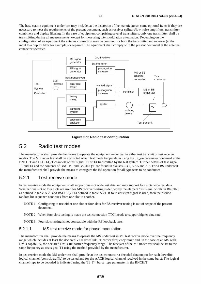
ETSI
ETSI EN 300 394-1 V3.3.1 (2015-04)16
The base station equipment under test may include, at the discretion of the manufacturer, some optional items if they are necessary to meet the requirements of the present document, such as receiver splitters/low noise amplifiers, transmitter combiners and duplex filtering. In the case of equipment comprising several transmitters, only one transmitter shall be transmitting during all measurements, except for measuring intermodulation attenuation. Depending on the configuration of an equipment the antenna connection may be common for both the transmitter and receiver (at the input to a duplex filter for example) or separate. The equipment shall comply with the present document at the antenna connector specified.
RF signal generator
RF signal generator
propagation simulator
(test transceiver)
tester error rate
timing meas.
sampling system
spectrum analyser
propagation simulator
splitter
combiner
wanted signal
isolating device
MS or BS under test
MS or BS antenna connector
Test connector
Test transmit
Bus interface Test
System
Controller
Tx
2nd Interferer
1st Interferer
Figure 5.1: Radio test configuration
5.2 Radio test modes The manufacturer shall provide the means to operate the equipment under test in either test transmit or test receive modes. The MS under test shall be instructed which test mode to operate in using the Tx_on parameter contained in the BNCH/T and BSCH-Q/T channels of test signal T1 or T4 transmitted by the test system. Further details of test signal T1 and T4 and the contents of BNCH/T and BSCH-Q/T are found in clauses 5.3.2, 5.3.5 and A.3. For a BS under test the manufacturer shall provide the means to configure the BS operation for all type tests to be conducted.
5.2.1 Test receive mode
In test receive mode the equipment shall support one slot wide test data and may support four slots wide test data. Whether one slot or four slots are used for MS receiver testing is defined by the element 'test signal width' in BNCH/T as defined in table A.20 and BSCH-Q/T as defined in table A.21. If four slots test signal is used, then the pseudo random bit sequence continues from one slot to another.
NOTE 1: Configuring to use either one slot or four slots for BS receiver testing is out of scope of the present document.
NOTE 2: When four slots testing is made the test connection TTCI needs to support higher data rate.
NOTE 3: Four slots testing is not compatible with the RF loopback tests.
5.2.1.1 MS test receive mode for phase modulation
The manufacturer shall provide the means to operate the MS under test in MS test receive mode over the frequency range which includes at least the declared V+D downlink RF carrier frequency range and, in the case of an MS with DMO capability, the declared DMO RF carrier frequency range. The receiver of the MS under test shall be set to the same frequency as test signal T1 using the method provided by the manufacturer.
In test receive mode the MS under test shall provide at the test connector a decoded data output for each downlink logical channel (control, traffic) to be tested and for the AACH logical channel received in the same burst. The logical channel type to be decoded is indicated using the T1_T4_burst_type parameter in the BNCH/T.

ETSI
ETSI EN 300 394-1 V3.3.1 (2015-04)17
In all cases whenever the MS decodes a timeslot containing BSCH and BNCH/T the MS shall provide the data decoded from these channels and from the AACH channel received on the same burst at the test connector. In the case where the MS detects an erroneous message on the BSCH or BNCH/T transmitted by the test equipment during frame 18, the MS shall remain in the same state as it was on frames 1 to 17.
5.2.1.2 BS test receive mode for phase modulation
Using the method provided by the manufacturer, the BS in test receive mode shall be configured to receive the desired logical channel type from the test system. The BS shall operate in its normal mode and provide at the test connector the decoded data output of each uplink logical channel tested.
The BS shall be configured to receive the desired logical channel on timeslot 1 of each uplink frame 1 … 17. During testing the test system shall use the down link BS transmissions to synchronize its uplink burst frequency and timing. The BS may transmit in timeslot 1 of frame 18 a downlink synchronization burst according to table 5.1.
Table 5.1: Base Station down link synchronization burst
Burst type Block 1 Block 2 Broadcast Block synchronization BSCH BNCH/T AACH
The downlink synchronization burst contains both BSCH and BNCH/T channels, which includes the T1_T4_burst_type parameter indicating the logical channel the BS is expecting to receive. The BNCH/T is a logical channel specific to the test mode. The contents of the BSCH and BNCH/T channels used during testing are defined in clause A.3. For a BS in continuous mode time slots 1 to 4 of downlink frames 1 to 17 and time slots 2 to 4 of downlink frame 18 are filled with a channel type 1 signal, see clause 5.3.2 for details of channel types. For a BS in discontinuous mode time slot 1 of downlink frames 1 to 17 are filled with a channel type 1 signal.
The values of MCC + MNC + BCC in the BSCH shall form the 30 bits of the extended colour code which is used to generate the scrambling sequence for all downlink and uplink logical channels, except for the BSCH itself where the 30 bits shall be set equal to zero. The test equipment shall use the scrambling sequence indicated by the BS under test.
Unless otherwise specified the following configuration shall be used:
• channel type 1 (see clause 5.3.2 for details);
• the parameters MS_TXPWR_MAX_CELL shall be set to 15 dBm;
• the parameter ACCESS_PARAMETER shall be set to -53 dBm.
The downlink synchronization burst shall be used by the test system to synchronize its uplink sub burst frequency and timing.
In the case of testing a receive-only BS, the manufacturer shall also provide a BS transmitter and the required interconnections with the receive-only BS for synchronization purposes.
5.2.1.3 MS test receive mode for QAM (where supported)
The manufacturer shall provide the means to operate the MS under test in MS QAM test receive mode over the frequency range which includes at least the declared V+D downlink RF carrier frequency. The receiver of the MS under test shall be set to the same frequency and bandwidth as test signal T4 using the method provided by the manufacturer. The MS under test may synchronize to T4 by means of the phase modulation synchronization burst in slot 3 of frame 18 (clause 5.3.5), when testing CA MS performance on a QAM channel. This synchronization burst contains the BSCH and the BNCH/T logical channels.
The MS under test may synchronize to T4 by means of the QAM Frequency Correction Burst (FCB) in slot 1 of frame 18 (clause 5.3.5) when testing DA MS performance on a QAM channel. FCB contains the BSCH-Q/T logical channel.
ETSI
ETSI EN 300 394-1 V3.3.1 (2015-04)18
In test receive mode the MS under test shall provide at the test connector a decoded data output for the downlink payload logical channel to be tested (SCH-Q/D) and for the downlink header logical channels received in the same burst (SICH-Q/D and AACH-Q). The logical channel type to be decoded in the burst payload is indicated using the T1_T4_burst_type parameter in the BNCH/T or BSCH-Q/T. The modulation and code rate information of the payload logical channel is indicated using the QAM_payload_type parameter in the BNCH/T or BSCH-Q/T (i.e. not indicated in SICH-Q/D). The payload logical channel (SCH-Q/D) and the slot information channel (SICH-Q/D) each contain an independent pseudo random bit sequence for testing purposes; the SICH-Q/D therefore does not provide control information to the MS under test.
In the case where the CA MS detects an erroneous message on the BSCH or BNCH/T transmitted by the test equipment during frame 18, slot 3, the MS shall remain in the same state as it was on frames 1 to 17. In the case where the DA MS detects an erroneous message on the BSCH-Q/T transmitted by the test equipment during frame 18, slot 1, the MS shall remain in the same state as it was on frames 1 to 17.
5.2.1.4 BS test receive mode for QAM (where supported)
Using the method provided by the manufacturer, the BS in test receive mode shall be configured to receive the desired logical channel type from the test system. The BS shall operate in its normal mode and provide at the test connector the decoded data output of the uplink payload logical channel to be tested (SCH-Q/U or SCH-Q/HU) and for the uplink header logical channel received in the same burst (SICH-Q/U).
The BS shall be configured to receive the desired logical channel either on timeslot 1 or on all four of each uplink frame 1 … 17. The BS equipment shall provide a trigger signal which can be used by the test equipment for uplink synchronization (clause 4.1.1).
NOTE 1: Configuring to use either one slot or four slots for BS receiver testing is out of scope of the present document.
Frame 18, slot 1 may contain the BNCH-Q/T channels, which includes the T1_T4_burst_type parameter indicating the logical channel the BS is expecting to receive in the burst payload and the QAM_payload_type parameter indicating the modulation and code rate information the BS is expecting to be used in the received burst payload. The BNCH-Q/T is a logical channel specific to the test mode. The contents of the BNCH-Q/T channels used during testing are defined in clause A.3. Time slots 1 through 4 of downlink frames 1 to 17 and slots 2 through 4 of downlink frame 18 are filled with a channel type 27 signal, see clause 5.3.5 for details of channel types.
NOTE 2: BNCH-Q/T is sent on 25 kHz QAM channel using 4-QAM modulation level with coding rate r=1/2. The test equipment will ignore the received SICH-Q, which is scrambled by using the normal scrambling sequence.
The values of MCC + MNC + BCC in the BNCH-Q/T shall form the 30 bits of the extended colour code which is used to generate the scrambling sequence for all downlink and uplink logical channels, except for the BNCH-Q/T itself where the 30 bits shall be set equal to zero. The test equipment shall use the scrambling sequence indicated by the BS under test.
Unless otherwise specified the following configuration shall be used:
• channel type 27 (see clause 5.3.2 for details);
• the parameters MS_TXPWR_MAX_CELL shall be set to 15 dBm;
• the parameter ACCESS_PARAMETER shall be set to -53 dBm.
In the case of testing a receive-only BS, the manufacturer shall also provide a BS transmitter and the required interconnections with the receive-only BS for synchronization purposes.
ETSI
ETSI EN 300 394-1 V3.3.1 (2015-04)19
5.2.2 Test transmit mode
5.2.2.1 MS testing for phase modulation
The manufacturer shall provide the means to operate the MS under test in MS test transmit mode using phase modulation over the frequency range which includes at least the declared V+D uplink RF carrier frequency range and, in the case of an MS with DMO capability, the declared DMO RF carrier frequency range. In test transmit mode, the MS under test may use the Main Carrier, Frequency Band, Offset, Duplex Spacing and Reverse Operation parameters contained in the BNCH/T channel of test signal T1 to set its transmit frequency. If the MS duplex spacing or reverse operation capabilities are fixed, the MS shall ignore these parameters. In test transmit mode the MS under test shall transmit either a normal uplink burst or control uplink burst, as indicated by the Tx_Burst_type parameter of the BNCH/T. The MS shall transmit a π/4-DQPSK modulated signal type if the T1_T4_burst_type is a π/4-DQPSK modulated signal type. Where supported, a π/8-D8PSK modulated signal type shall be used by the MS if the T1_T4_burst_type is a π/8-D8PSK modulated signal type. The MS shall be synchronized in time and frequency to the test signal T1 and shall transmit only on timeslot 1.
In test transmit mode the MS shall begin by transmitting a typical CLCH burst on subslot 1 of frame 18 followed by transmission of TCH/7,2 or TCH-P8/10,8 normal uplink bursts on frames 1 to 17, or SCH/HU or SCH-P8/HU control uplink burst on subslot 1 of frames 1 to 17, the sequence then repeating. Further CLCH opportunities are therefore available every multiframe. A bit stream, produced by repeating a pseudo random sequence with a length of 511 bits according to Recommendation ITU-T O.153 [2], shall be used as the information to be transmitted over the logical channel, the sequence then continues across multiframes without breaks after the CLCH slots. The MS shall set its transmit power according to the measured signal strength of signal T1 and the decoded power control parameters in the BNCH/T channel.
In all MS transmitter testing the test system shall continuously transmit test signal T1 with channel type 1 (TCH/7,2) or channel type 21 (TCH-P8/10,8) in timeslot 1 of frames 1 to 17 and synchronization burst containing a BSCH and BNCH/T in timeslot 1 of frame 18. In timeslots 2 to 4 of frames 1 to 18 channel type 0 shall be transmitted.
In test transmission mode the MS shall continue to monitor the BSCH and BNCH/T transmitted by the test equipment on frame 18.
5.2.2.2 Void
5.2.2.3 BS testing for phase modulation
Using the method provided by the manufacturer, the BS in test transmit mode shall be configured to transmit the desired down link logical channel and burst/sub burst type. The BS shall operate in its normal mode e.g. continuous or discontinuous mode. For a BS in discontinuous mode the BS shall transmit only in time slot 1 of each frame. A bit stream, produced by repeating a pseudo random sequence with a length of 511 bits according to Recommendation ITU-T O.153 [2], shall be used as the information to be transmitted over the logical channel. The BS transmission may begin with a BLCH burst and, if required, shall include further BLCH bursts not exceeding one occurrence per four multiframe periods, which shall only occur in block 2 of a Normal Downlink Burst with SCH/HD in block 1 (using Normal Training sequence 2) defined in ETSI EN 300 392-2 [1], clause 9.
The BS shall transmit in timeslot 1 of frame 18, a synchronization burst containing BSCH and BNCH/T information. A BS operating in continuous mode shall transmit a channel type 1 signal in time slots 1 to 4 of frames 1 to 17 and time slots 2 to 4 in frame 18. A BS operating in discontinuous mode shall transmit a channel type 1 signal in timeslot 1 of frames 1 to 17 only.
5.2.2.4 MS testing for QAM (where supported)
The manufacturer shall provide the means to operate the MS under test in MS test transmit mode using QAM over the frequency range which includes at least the declared V+D uplink RF carrier frequency range. The MS under test shall be able to transmit the 8, 16, 32, or 48 subcarrier control up-link burst or normal up-link burst. In test transmit mode, the MS under test may use the Main Carrier, Frequency Band, Offset, Duplex Spacing and Reverse Operation parameters contained in the BNCH/T or BSCH-Q/T channel of test signal T4 to set its transmit frequency. If the MS duplex spacing or reverse operation capabilities are fixed, the MS shall ignore these parameters.
NOTE 1: BNCH/T is used when CA MS performance on a QAM channel is tested. BSCH-Q/T is used when DA MS performance on a QAM channel is tested.
ETSI
ETSI EN 300 394-1 V3.3.1 (2015-04)20
In test transmit mode the MS under test shall transmit either a normal uplink burst or control uplink burst, as indicated by the Tx_Burst_type parameter of the BNCH/T or BSCH-Q/T. The MS shall be synchronized in time and frequency to the test signal T4 and shall transmit only on timeslot 1.
In test transmit mode the MS may begin by transmitting a typical CLCH-Q burst on subslot 1 of uplink timeslots 1 or 3 of frame 18 followed by transmission of SCH-Q/U normal uplink bursts on frames 1 to 17, or SCH-Q/HU control uplink burst on subslot 1 of frames 1 to 17, the sequence then repeating. The SCH-Q/U or SCH-Q/HU logical channel contains K4 type-4 bits and they are only scrambled as in ETSI EN 300 392-2 [1], clause 8.3.2.5 or clause 8.3.2.4, i.e. only encoding of type-4 bits into type-5 bits is applicable, excluding coding of type-1 bits into type-4 bits. The SICH-Q/U logical channel is encoded normally as in ETSI EN 300 392-2 [1], clause 8.3.2.1, i.e. 5 type-1 bits are encoded into 16 type-5 bits. Further CLCH-Q opportunities are therefore available every multiframe. A bit stream, produced by repeating a pseudo random sequence with a length of 511 bits according to Recommendation ITU-T O.153 [2], shall be used as the information to be transmitted over the logical channel, the sequence then continues across multiframes without breaks after the CLCH-Q slots.
NOTE 2: Continuing the pseudo random bit sequence without breaks from one multiframe to the next is required for randomization of the data patterns across multiple transmitted burst measurements. The 'PRBS continuation' element in the BNCH/T or BSCH-Q/T does not provide control information to the MS in test transmission mode.
The SICH-Q/U logical channel does not provide valid slot information but carries a separate continuous pseudo random bit sequence of length 511 bits which is independent of the bit sequence in the SCH-Q/U or SCH-Q/HU logical channel. The MS shall set its transmit power according to the measured signal strength of signal T4 and the decoded power control parameters in the BNCH/T or BSCH-Q/T channel. The MS shall set its transmit bandwidth and QAM type the same as the received downlink T4 signal according to the 'carrier bandwidth' and 'QAM_payload_type' parameters in the BNCH/T or BSCH-Q/T channel, always transmitting uncoded (only scrambled) regardless of the indication of the downlink rate as 1/2, 2/3 or 1.
NOTE 3: When linearizing the amplifier on the subslot 1 of frame 18, the CA MS is not able to receive and decode the BSCH and BNCH/T and therefore the MS may need to postpone the linearization to the next multiframe. The CA MS may also choose to linearize immediately on subslot 1 of uplink timeslot 3 of frame 18; in this case the CA MS is not able to receive and decode the downlink timeslot 1 of frame 1, but is able to receive and decode the BSCH and BNCH/T.
In all MS transmitter testing the test system shall continuously transmit test signal T4 with channel type 27 (SCH-Q/D) in timeslot 1 of frames 1 to 17 and a synchronization containing a BSCH and BNCH/T, or a BSCH-Q/T, in frame 18 (clause 5.3.5).
In test transmission mode the MS shall continue to monitor the BSCH and BNCH/T, or a BSCH-Q/T, transmitted by the test equipment on frame 18, except when the MS needs to linearize the amplifier and is thus unable to monitor BSCH and BNCH/T, or BSCH-Q/T in the same frame 18.
5.2.2.5 BS testing for QAM (where supported)
Using the method provided by the manufacturer, the BS in test transmit mode shall be configured to transmit the SCH-Q/D logical channel type with 8, 16, 32, or 48 subcarriers and 4-QAM, 16-QAM, or 64-QAM modulation. A bit stream, produced by repeating a pseudo random sequence with a length of 511 bits according to Recommendation ITU-T O.153 [2], shall be used as the information to be transmitted over the logical channel. The pseudo random sequence shall continue without breaks from one multiframe to another.
The BS transmission may begin with a BLCH-Q burst and, if required, shall include further BLCH-Q bursts not exceeding one occurrence per four multiframe periods.
The BS shall transmit in frame 18, slot 1 a BNCH-Q/T logical channel (see clause A.3). The BS equipment shall provide a trigger signal which can be used by the test equipment synchronization (clause 4.1.1). A BS shall transmit a channel type 27 signal in time slots 1 to 4 of frames 1 to 17 and slot 2 to 4 of frame 18.

ETSI
ETSI EN 300 394-1 V3.3.1 (2015-04)21
5.3 Radio test signals
5.3.1 General
In principle the modulation of the test signals T1, to be described below, shall comply with ETSI EN 300 392-2 [1], clause 5. The modulation filter is specified by a set of windowed discrete impulse response samples, {g'j}, where
j = 0...N-1 and,
where g(t) is the symbol waveform defined in ETSI EN 300 392-2 [1], clause 5, Ns is the number of symbols spanned by the filter and T is the symbol duration as defined in ETSI EN 300 392-2 [1], clause 5. Ns shall be at least 15. The window coefficients, wj, are defined by:
The test transmitter shall be sufficiently linear with respect to amplitude and phase (active linearization should be avoided whenever possible) to meet the requirements in clause B.1.
5.3.2 Test signal T1 (TETRA wanted signal, phase modulation)
The T1 signal sequence shall comply with the TETRA air interface multiframe, frame and slot/burst/sub burst structure and is the wanted signal transmitted by the test system during frames 1 to 17 in all receiver tests. The modulation type shall be π/4-DQPSK or π/8-D8PSK (where supported). The information transmitted by the test system in frame 18 of T1 is used for test control purposes. The slot structure of T1 in frames 1 to 17 is dependent upon the type of receiver test being conducted, defined by the channel type number.
5.3.2.1 MS testing
During MS receiver testing, the test system shall transmit in timeslot 1 of T1 continuous down link burst and channel types according to the tables 5.2 and 5.3.
On frame 18 according to table 5.2.
Table 5.2: Test system transmission
Burst type Block 1 Block 2 Broadcast Block synchronization BSCH BNCH/T AACH
The BNCH/T is a logical channel specific to the test mode. The contents of the BSCH and BNCH/T to be used during the test are given in clause A.3. The Main Carrier, Frequency Band and Offset parameters contained in the BNCH/T shall indicate the downlink frequency of the T1 test signal being generated. The Duplex Spacing and Reverse Operation parameters contained in the BNCH/T shall indicate the required uplink frequency with respect to the indicated downlink frequency. These parameters are defined in ETSI EN 300 392-2 [1], clause 21.
On frame 1 to 17 one of the following channel types according to table 5.3.
g w g TNj
Nj j s' =
−−
⎛
⎝⎜
⎞
⎠⎟
⎛
⎝⎜
⎞
⎠⎟
1
1
2
( )
( )w
j N
Nj = −
− −
+
⎛
⎝
⎜⎜⎜
⎞
⎠
⎟⎟⎟
1
1
21
1
21
2
ETSI
ETSI EN 300 394-1 V3.3.1 (2015-04)22
Table 5.3: Channel types
Channel type Burst type Block 1 Block 2 Broadcast Block 0 normal TCH/7,2 AACH 1 normal TCH/7,2 AACH 2 normal SCH/F AACH 3 synchronization BSCH SCH/HD AACH 4 normal TCH/2,4, N = 1 AACH 21 normal TCH-P8/10,8 AACH 22 normal SCH-P8/HD AACH 24 normal SCH-P8/F AACH
The T1 signal shall be scrambled according to ETSI EN 300 392-2 [1], clause 8, using the scrambling sequence generated from the 30 bits of the extended colour code, except for the BSCH where the 30 bits shall be set equal to zero. The extended colour code shall be formed from the values of MCC + MNC + BCC which are transmitted in the T1 signal BSCH information defined in table A.15. The MS under test shall use the scrambling sequence indicated by the T1 signal.
A bit stream, produced by repeating a pseudo random sequence with a length of 511 bits according to Recommendation ITU-T O.153 [2], shall be used as the information to be transmitted over the logical channel to be tested. Unless otherwise specified the contents of any logical channels not currently being tested is undefined. The test system shall support at least one of the pseudo random bit sequence alternatives:
• sequence continues without breaks from one multiframe to another; or
• sequence is repeated for each multiframe starting with frame 1, timeslot 1.
The indication of the sequence type may be defined in BNCH/T, see table A.20.
NOTE: For channel type 3, the logical channels BNCH and STCH have the same coding, interleaving format and performance specification as SCH/HD and are not, therefore, specifically tested.
Channel types 1, 2, 3, 4, 21, 22 and 24 shall be tested in continuous transmission mode where channel type 0 is inserted in time slots 2 to 4 of frames 1 to 18.
For MS synchronization burst acquisition performance testing, the normal multiframe structure shall not be respected and the synchronization continuous downlink bursts (including start and stop bursts) carrying BSCH/T shall be transmitted randomly. The period between the start of two synchronization bursts shall be randomly selected in the range between 800 and 25 000 symbol durations, with a step less than or equal to ¼ symbol duration. Nothing shall be transmitted in the time interval between synchronization bursts. This special transmission mode is defined as channel type 13.
5.3.2.2 BS testing
During BS receiver testing the test system shall transmit in timeslot 1 of T1 up link burst and channel types according to the tables 5.4 and 5.5.
On frame 18 according to table 5.4.
Table 5.4: Test system transmission
Channel type Burst type Block 1 Block 2 8 normal SCH/F
On frame 1 to 17 one of the following channel types according to table 5.5.
ETSI
ETSI EN 300 394-1 V3.3.1 (2015-04)23
Table 5.5: Channel types
Channel type Burst type Block 1 / Sub slot 1 Block 2 / Sub slot 2 7 normal TCH/7,2 8 normal SCH/F 9 normal STCH STCH 10 normal TCH/2,4, N = 1 11 control SCH/HU SCH/HU 21 normal TCH-P8/10,8 23 normal SCH-P8/HU 24 normal SCH-P8/F
For BS receiver testing, channel type 7 shall be inserted in time slots 2 to 4 of all uplink frames 1 to 18. A bit stream, produced by repeating a pseudo random sequence with a length of 511 bits according to Recommendation ITU-T O.153 [2], shall be used as the information to be transmitted over the logical channel.
5.3.2.3 Void
5.3.2.4 Void
5.3.3 Test signal T2 (TETRA interferer)
The phase modulated test signal T2 is a π/4-DQPSK modulated continuous radio signal following the structure of TETRA signals, but with all modulating bits (including training sequences) derived directly from pseudo random bit sequence (with a length of 511 bits according to Recommendation ITU-T O.153 [2]).
The QAM modulated test signal T2 is a 4-QAM, 16-QAM, or 64-QAM modulated continuous signal with a bandwidth of 25 kHz, 50 kHz, 100 kHz, or 150 kHz following the structure of TEDS signals, but with all modulating symbols' underlying bits (including synchronization and pilot symbols) derived directly from pseudo random bit sequence (with a length of 511 bits according to Recommendation ITU-T O.153 [2]).
T2 is used as an unwanted (modulated) signal.
5.3.4 Test signal T3 (unmodulated interferer)
Test signal T3 is an unmodulated continuous sinusoidal radio signal. T3 is used as an unwanted (unmodulated) signal.
5.3.5 Test signal T4 (TETRA wanted signal, QAM)
The T4 signal sequence shall comply with the TETRA air interface multiframe, frame and slot/burst/sub burst structure and is the wanted signal transmitted by the test system during all QAM receiver tests.
The bandwidth of T4 shall be 25 kHz, 50 kHz, 100 kHz, or 150 kHz during QAM modulation, and 25 kHz during π/4-DQPSK modulation.
5.3.5.1 MS testing
The slot structure of T4 for downlink in frames 1 to 17 is that of the normal downlink burst for QAM modulation.
a) CA MS testing
In the case that CA MS performance is tested, π/4-DQPSK modulation shall be transmitted in part of frame 18. The π/4-DQPSK information transmitted by the test system in frame 18 slot 3 of T4 is used for test control purposes. The structure of the π/4-DQPSK transmission in frame 18 is defined in clause 5.3.5.1.1.
During CA MS receiver testing, the test system shall transmit T4 continuous down link burst and channel types according to the tables 5.2 and 5.5b.
On timeslot 3 of frame 18 according to table 5.2.
On frame 1 to 17 one of the channel types according to table 5.5b.

ETSI
ETSI EN 300 394-1 V3.3.1 (2015-04)24
b) DA MS testing
In the case that DA MS performance is tested, QAM modulation shall be transmitted in part of frame 18. The 4-QAM information transmitted by the test system in frame 18 slot 1 of T4 is used for test control purposes. The structure of the QAM transmission in frame 18 is defined in clause 5.3.5.1.1a.
During DA MS receiver testing, the test system shall transmit T4 continuous down link burst and channel types according to the tables 5.5a and 5.5b.
On timeslot 1 of frame 18 according to table 5.5a.
Table 5.5a: Test system transmission
Burst type Frequency correction data set A Slot header frequency correction BSCH-Q/T AACH-Q and
SICH-Q/D
The BSCH-Q/T is a logical channel specific to the test mode. The contents of the BSCH-Q/T to be used during the test are given in clause A.3. The Main Carrier, Frequency Band and Offset parameters contained in the BSCH-Q/T shall indicate the downlink frequency of the T4 test signal being generated. The Duplex Spacing and Reverse Operation parameters contained in the BSCH-Q/T shall indicate the required uplink frequency with respect to the indicated downlink frequency. These parameters are defined in ETSI EN 300 392-2 [1], clause 21.
On frame 1 to 17 one of the channel types according to table 5.5b.
c) CA and DA MS testing
During both CA MS receiver testing and DA MS receiver testing, the test system shall continuously transmit test signal T4 with channel type 27 (SCH-Q/D) in timeslot 1 of frames 1 to 17, if one slot testing is used, and in timeslots 1 to 4 of frames 1 to 17, if four slots testing is used.
Table 5.5b: Channel types
Channel type Burst type Downlink data set Slot header 27 normal SCH-Q/D AACH-Q and
SICH-Q/D 27a normal SCH-Q/D AACH-Q and
SICH-Q/D
The pseudo random bit sequence continues from one used slot to another. If one slot testing is used, the test system shall continuously transmit test signal T4 with channel type 27a (SCH-Q/D) in timeslots 2 to 4 of frames 1 to 17. Channel type 27a is not intended to be received and decoded by the MS under test; its content is undefined and is independent of the content of channel type 27. The test system shall transmit on frame 18 according to clause 5.3.5.1.1. The T4 signal shall be scrambled according to ETSI EN 300 392-2 [1], clause 8, using the scrambling sequence generated from the 30 bits of the extended colour code, except for the BSCH or BSCH-Q/T where the 30 bits shall be set equal to zero. The extended colour code shall be formed from the values of MCC + MNC + BCC which are transmitted in the T4 signal BSCH information defined in table A.19 or BSCH-Q/T information defined in table A.21. The MS under test shall use the scrambling sequence indicated by the T4 signal.
A bit stream, produced by repeating a pseudo random sequence with a length of 511 bits according to Recommendation ITU-T O.153 [2], shall be used as the information to be transmitted over the logical channel to be tested. The test system shall support at least one of the pseudo random bit sequence alternatives:
• sequence continues without breaks from one multiframe to another; or
• sequence is repeated for each multiframe starting with frame 1, timeslot 1.
The indication of the sequence type may be defined in BNCH/T, see table A.20 and in BSCH-Q/T, see table A.21.
The SICH-Q/D logical channel and the AACH-Q logical channel do not provide valid control information in the T4 test signal: each logical channel carries a separate continuous pseudo random bit sequence of length 511 bits which is independent of the bit sequence in the SCH-Q/D logical channel. Unless otherwise specified the contents of any logical channels not currently being tested is undefined.
ETSI
ETSI EN 300 394-1 V3.3.1 (2015-04)25
NOTE 1: QAM-SLOTINFO has no meaning in the slot header of data stream, which follows the T4 signal. Modulation and code rate information in these slots is indicated by the information element QAM_payload_type in BSCH-Q/T, BNCH-Q/T or BNCH/T channel.
One or four slots may be used for test data, when MS is tested. Whether one slot or four slots are used for testing is defined by the element "test signal width" in BNCH/T as defined in Table A.20 and BSCH-Q/T as defined in table A.21.
NOTE 2: When four slots testing is made the test connection TTCI needs to support higher data rate.
NOTE 3: Four slots testing is not compatible with the RF loopback tests.
5.3.5.1.1 Use of synchronization burst in frame 18 when testing CA MSs
Figure 5.2 illustrates the method in which the test equipment's power, modulation type and RF bandwidth vary with time in the T4 signal.
In figure 5.2, a phase modulation synchronization continuous downlink burst is transmitted during frame 18 slot 3. The QAM signal under test is transmitted during all slots of frames 1 to 17.
The MS under test shall monitor the BNCH/T logical channel transmitted in frame 18 slot 3 in order to detect any changes in the type of test being indicated.
Figure 5.2 shows that frame 17 slot 4 contains a QAM burst transmitted at the RF power level PQ required for the
particular QAM FER and BER measurement in QAM bandwidth fQ (which may be 25 kHz, 50 kHz, 100 kHz or
150 kHz, according to the test in progress).
Frame 18 slot 1 contains the first two symbols SN-Q1 and SN-Q2 of a new QAM burst at the same RF power level and RF bandwidth – these contain synchronization pilot symbols and are provided to allow the MS to interpolate back into frame 17 slot 4 for channel estimation purposes.
From just after the symbol time of SN-Q2 until 0,5 QAM symbol periods after symbol time SN-Q4 the test equipment may ramp its QAM signal down to zero RF level (i.e. from 3 750/9 μs until 13 125/9 μs after the start of slot 1). After ramping down the RF output shall then remain at zero power until symbol time SN133 of slot 2).
NOTE: A slot starts at symbol times SN0 and SN-Q1 (ETSI EN 300 392-2 [1], clauses 7.3.2 and 7.5.1).
Frame 18 slot 1 after SN-Q2 is used for the QAM frequency correction burst (FCB) when DA MS performance is tested, see clause 5.3.5.1.1a. A CA MS is not required to decode any transmissions it receives in frame 18 slot 1 after SN-Q2.
After the symbol time SN133 of slot 2 (i.e. 66 500/9μs after the start of slot 2), the test equipment shall ramp up and transmit π/4-DQPSK symbols. This transmission shall be at the same power as frame 18 slot 3 and may be used by the MS for AGC purposes. The test equipment shall transmit a synchronization continuous down-link burst in slot 3, commencing with the first five symbols of the π/4-DQPSK normal training sequence 3 as symbols SN251 to SN255 of frame 18 slot 2 (slot 2 symbol time SN251 occurs 125 500/9 μs after the start of slot 2).
The synchronization continuous downlink burst sent in slot 3 has the form shown for the T1 test signal in clause 5.3.2.1 for frame 18 slot 1 of the T1 test signal. It contains BSCH in block 1 and BNCH/T in block 2. The synchronization continuous downlink burst includes the π/4-DQPSK normal training sequence 3 at the start and end of slot 3. The last six symbols of the π/4-DQPSK normal training sequence 3 at the end of slot 3 extend into slot 4, comprising symbols SN1 to SN6 of slot 4. The π/4-DQPSK signalling shall be transmitted in a 25 kHz bandwidth.
The phase modulation transmission shall be aligned so that symbol time SN0 for slot 3 occurs 255 000/9 μs ±125/9 μs after the start of frame 18 slot 1. The centre frequency of the phase modulation transmission shall be the same as the centre frequency of the QAM channel.
The mean power level of the phase modulation transmission should be user-adjustable in the range -115 dBm to -20 dBm. The mean power level of the QAM transmission in frames 1 to 17 may be above or below this level, depending on the type of test.
Transmission of phase modulation stops at the end of the π/4-DQPSK normal training sequence 3 that terminates on symbol SN6 of frame 18 slot 4 (i.e. at 3 000/9 μs after the start of slot 4). The phase modulation is ramped down to zero RF power from symbol times SN6 until SN21 (i.e. from 3 000/9 μs until 10 500/9 μs after the start of slot 4).
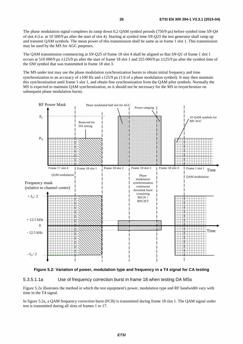
ETSI
ETSI EN 300 394-1 V3.3.1 (2015-04)26
The phase modulation signal completes its ramp down 0,2 QAM symbol periods (750/9 μs) before symbol time SN-Q4 of slot 4 (i.e. at 10 500/9 μs after the start of slot 4). Starting at symbol time SN-Q25 the test generator shall ramp up and transmit QAM symbols. The mean power of this transmission shall be same as in frame 1 slot 1. This transmission may be used by the MS for AGC purposes.
The QAM transmission commencing at SN-Q25 of frame 18 slot 4 shall be aligned so that SN-Q1 of frame 1 slot 1 occurs at 510 000/9 μs ±125/9 μs after the start of frame 18 slot 1 and 255 000/9 μs ±125/9 μs after the symbol time of the SN0 symbol that was transmitted in frame 18 slot 3.
The MS under test may use the phase modulation synchronization bursts to obtain initial frequency and time synchronization to an accuracy of ±100 Hz and ±125/9 μs (1/4 of a phase modulation symbol). It may then maintain this synchronization until frame 1 slot 1, and obtain fine synchronization from the QAM pilot symbols. Normally the MS is expected to maintain QAM synchronization, so it should not be necessary for the MS to resynchronize on subsequent phase modulation bursts.
Frame 17 slot 4
Frame 18 slot 1
Frame 18 slot 2
Frame 18 slot 3
Frame 18 slot 4
Frame 1 slot 1
RF Power Mask
Time
Time
QAM modulation
Phase modulation
synchronisation continuous
downlink burst containing BSCH + BNCH/T
Phase modulated half slot for AGC
QAM modulation
10 QAM symbols for MS AGC
Pp
PQ
Frequency mask (relative to channel centre)
0
- 12.5 kHz
+ fQ / 2
Power ramping
Reserved for DA testing
+ 12.5 kHz
- fQ / 2
Figure 5.2: Variation of power, modulation type and frequency in a T4 signal for CA testing
5.3.5.1.1a Use of frequency correction burst in frame 18 when testing DA MSs
Figure 5.2a illustrates the method in which the test equipment's power, modulation type and RF bandwidth vary with time in the T4 signal.
In figure 5.2a, a QAM frequency correction burst (FCB) is transmitted during frame 18 slot 1. The QAM signal under test is transmitted during all slots of frames 1 to 17.
ETSI
ETSI EN 300 394-1 V3.3.1 (2015-04)27
The MS under test shall monitor the BSCH-Q/T logical channel transmitted in frame 18 slot 1 in order to detect any changes in the type of test being indicated. In case continuous QAM transmission is used, the slots 2 to 4 in frame 18 include SCH-Q/D without any useful information.
Figure 5.2a shows that frame 17 slot 4 contains a QAM burst transmitted at the RF power level PQ required for the
particular QAM FER and BER measurement in QAM bandwidth fQ (which may be 25 kHz, 50 kHz, 100 kHz or
150 kHz, according to the test in progress).
The FCB shall be transmitted with the same RF bandwidth, frequency and mean power level as the transmissions in frames 1 to 17.
During the period between symbol time of SN-Q2 of slot 2 and 0,5 QAM symbol periods after symbol time SN-Q4 of slot 2 (i.e. from 3 750/9 μs until 13 125/9 μs after the start of slot 2) the QAM transmission may ramp down to zero RF level. The RF output shall then remain at zero power until at least symbol time SN133 of slot 2 (i.e. 66 500/9 μs after the start of slot 2). Alternatively, the QAM transmission may be continuous over the frame 18.
NOTE 1: A slot starts at symbol times SN0 and SN-Q1 (ETSI EN 300 392-2 [1], clauses 7.3.2 and 7.5.1).
In frame 18 slot 4 starting at symbol time SN-Q25 the test generator shall ramp up (if not already transmitting) and shall transmit QAM symbols. The mean power of this transmission shall be same as in frame 1 slot 1. This transmission may be used by the MS for AGC purposes.
The QAM transmission commencing at SN-Q25 of frame 18 slot 4 shall be aligned so that SN-Q1 of frame 1 slot 1 occurs at 510 000/9 μs ±125/9 μs after the start of frame 18 slot 1.
The MS under test may use the FCB to obtain initial frequency and time synchronization to an accuracy of ±100 Hz and ±125/9 μs. The MS is then expected to maintain QAM synchronization from the QAM pilot symbols in the SCH-Q/D transmissions in frames 1 to 17. It should not be necessary for the MS to resynchronize on subsequent FCBs.
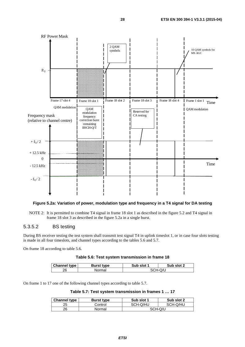
ETSI
ETSI EN 300 394-1 V3.3.1 (2015-04)28
QAM modulation frequency
correction burst containing BSCH-Q/T
+ fQ / 2
- fQ / 2
Reserved for CA testing
2 QAM symbols
Frame 17 slot 4
Frame 18 slot 1
Frame 18 slot 2
Frame 18 slot 3
Frame 18 slot 4
Frame 1 slot 1
RF Power Mask
Time
Time
QAM modulation
QAM modulation
10 QAM symbols for MS AGC
PQ
Frequency mask (relative to channel centre)
0
- 12.5 kHz
+ 12.5 kHz
Figure 5.2a: Variation of power, modulation type and frequency in a T4 signal for DA testing
NOTE 2: It is permitted to combine T4 signal in frame 18 slot 1 as described in the figure 5.2 and T4 signal in frame 18 slot 3 as described in the figure 5.2a in a single burst.
5.3.5.2 BS testing
During BS receiver testing the test system shall transmit test signal T4 in uplink timeslot 1, or in case four slots testing is made in all four timeslots, and channel types according to the tables 5.6 and 5.7.
On frame 18 according to table 5.6.
Table 5.6: Test system transmission in frame 18
Channel type Burst type Sub slot 1 Sub slot 2 26 Normal SCH-Q/U
On frame 1 to 17 one of the following channel types according to table 5.7.
Table 5.7: Test system transmission in frames 1 … 17
Channel type Burst type Sub slot 1 Sub slot 2 25 Control SCH-Q/HU SCH-Q/HU 26 Normal SCH-Q/U
ETSI
ETSI EN 300 394-1 V3.3.1 (2015-04)29
In case channel type 25 is used the data stream is inserted in Sub slot 1 and Sub slot 2.
For BS receiver testing, in case 1 slots testing is made, channel type 26 shall be inserted in time slots 2 to 4 of all uplink frames 1 to 17. A bit stream, produced by repeating a pseudo random sequence with a length of 511 bits according to Recommendation ITU-T O.153 [2], shall be used as the information to be transmitted over the logical channel. The test system shall support at least one of the pseudo random bit sequence alternatives:
• sequence continues without breaks from one multiframe to another; or
• sequence is repeated for each multiframe starting with frame 1, timeslot 1.
NOTE: The selection of the type of pseudo random bit sequence in BS receiver testing is out of scope of the present document.
6 Test conditions
6.1 General Type tests shall be made under normal test conditions and where stated also under extreme test conditions. The test conditions and procedures shall be as specified in clauses 6.2.1 and 6.2.2.
6.2 Power sources and ambient conditions During type tests the power source of the equipment shall be replaced by a test power source, capable of producing normal and extreme test voltages as specified in clauses 6.2.1 and 6.2.2. The internal impedance of the test power source shall be low enough for its effect on the test results to be negligible. For the purpose of tests, the voltage of the power source shall be measured at the input terminals of the equipment. If the equipment is provided with a permanently connected power cable, the test voltage shall be that measured at the point of connection of the power cable to the equipment. In equipment with incorporated batteries the test power source shall be applied as close to the battery terminals as practicable. During tests the power source voltages shall be maintained within a tolerance of ±1 % relative to the voltage at the beginning of each test.
6.2.1 Normal test conditions
The normal temperature and humidity conditions for tests shall be any convenient combination of temperature and humidity within the common range fulfilling all of the following requirements:
• temperature +15 °C to +35 °C (degrees Celsius);
• relative humidity 5 % to 75 %;
• intended operational humidity range of the IUT.
When it is impracticable to carry out the tests under the conditions stated above, the actual temperature and relative humidity during the tests shall be recorded in the test report.
The normal test voltage for equipment to be connected to the mains shall be the nominal mains voltage. For the purpose of these specifications, the nominal voltage shall be the declared voltage or any of the declared voltages for which the equipment was designed. The frequency of the test power source corresponding to the mains shall be between 49 Hz and 51 Hz.
When the radio equipment is intended for operation from the usual types of regulated lead-acid battery power source of vehicles, the normal test voltage shall be 1,1 times the nominal voltage of the battery (6 V, 12 V, etc.).
For operation from other power sources or types of battery (primary or secondary) the normal test voltage shall be that declared by the equipment manufacturer.
ETSI
ETSI EN 300 394-1 V3.3.1 (2015-04)30
6.2.2 Extreme test conditions
For tests on equipment at extreme ambient temperatures measurements shall be made at an upper temperature and a lower temperature defined as follows:
• the lower temperature shall be -20 °C except for BS equipment where the lowest intended operational temperature of the BS shall apply if this is higher than -20 °C;
• the upper temperature shall be +55 °C except for BS equipment where the highest intended operational temperature of the BS shall apply if this is lower than +55 °C.
NOTE: The following equipment types are also classified as MS equipment for the purpose of environmental testing: V+D repeater, DM-MS, DW-MS, DM-REP, DM-GATE, DM-REP/GATE.
The extreme humidity conditions shall be the same as the normal humidity conditions specified in clause 6.2.1.
The extreme test voltages for equipment to be connected to an ac mains source shall be the nominal mains voltage ±10 %.
When the equipment is intended for operation from the usual types of regulated lead-acid battery power sources of vehicles the extreme test voltages shall be 1,3 times and 0,9 times the nominal voltage of the battery (6 V, 12 V, etc.).
The extreme test voltages for equipment with power sources using non regulated batteries shall be as follows. The upper extreme test voltage shall be the normal test voltage. The lower extreme test voltage shall be:
• for the Leclanché, nickel metal hybrid or the lithium-type of battery, 0,85 times the nominal voltage of the battery;
• for the mercury-type or nickel cadmium type of battery, 0,9 times the nominal voltage of the battery;
• for other types of batteries, end point voltage declared by the equipment manufacturer.
However, the lower extreme test source voltages shall be those agreed between the equipment manufacturer and the testing laboratory for the following equipment:
• designed to use other power sources;
• capable of being operated from a variety of power sources;
• designed to include a shut-down facility to ease operation of the equipment at source voltages other than those referred to above.
The conditions shall be recorded in the test report and in the latter case the purpose of including this facility.
The following four extreme test condition combinations are applied while testing TETRA equipment under extreme test conditions:
• LTLV: lower temperature and lower voltage;
• LTHV: lower temperature and higher voltage;
• HTLV: upper temperature and lower voltage;
• HTHV: upper temperature and higher voltage.
Unless otherwise stated tests to be conducted under extreme test conditions shall include all the above temperature and voltage combinations.
ETSI
ETSI EN 300 394-1 V3.3.1 (2015-04)31
6.3 Procedure for tests at extreme temperatures Before measurements are made, the equipment shall have reached thermal balance in the test chamber. The equipment shall be switched off during the temperature stabilizing period. In the case of equipment containing temperature stabilization circuits designed to operate continuously, the temperature stabilization circuits may be switched on for 15 minutes after thermal balance has been obtained, the equipment shall then meet the specified requirements. If the thermal balance is not checked by measurements, a temperature stabilizing period of at least one hour, or such period as may be decided by the testing laboratory shall be allowed. The sequence of measurements shall be chosen, and the humidity content in the test chamber shall be controlled so that excessive condensation does not occur.
6.3.1 Equipment designed for continuous operation
Before tests at the upper temperature, the equipment shall be placed in the test chamber and left until thermal balance is attained. The equipment shall then be switched on in the transmit state for a period of 30 minutes after which the equipment shall meet the specified requirements.
Before tests at the lower temperature, the equipment shall be left in the test chamber until thermal balance is attained, then switched to the idle (non-transmit) state for a period of 4 minutes, after which the equipment shall meet the specified requirements.
6.3.2 Equipment designed for intermittent operation
Before tests at the upper temperature, the equipment shall be placed in the test chamber and left until thermal balance is attained. The equipment shall then be switched on in the idle (non-transmit) state for a period of four minutes prior to testing. In the case of transmitter CLCH testing, measurement of unwanted emissions shall take place immediately following this period. Prior to further transmitter testing the equipment shall be operated in the transmit state for a period of one minute followed by four minutes in the idle (non-transmit) state before measurements are made.
Before tests at the lower temperature, the equipment shall be left in the test chamber until thermal balance is attained, then switched to the idle (non-transmit) state for a period of one minute after which the equipment shall meet the specified requirements.
7 Technical characteristics
7.1 Transmitter parameter definitions and limits
7.1.1 Transmitter output power
7.1.1.1 Definition
Power for phase modulation is defined as the average power, measured through TETRA filter, refer to clause B.1.2.2 defined in ETSI EN 300 392-2 [1], clause 5.5, over the useful part of the burst as defined in ETSI EN 300 392-2 [1], clause 9.
Power for QAM is defined as the sum of the powers of each of the sub-carriers within the RF channel bandwidth. For each sub-carrier, reference power is defined as the average power, measured at symbol time through the square root raised cosine filter defined in ETSI EN 300 392-2 [1], clause 5.16, over the pilot and sync symbols within the QAM burst as defined in ETSI EN 300 392-2 [1], clause 9.
For a bursted transmission, power for QAM and phase modulation is further defined by transmitter output power versus time.

ETSI
ETSI EN 300 394-1 V3.3.1 (2015-04)32
7.1.1.2 Limit values for phase modulation and QAM
The following requirements shall be met:
a) The average transmitter output power measured under the normal test conditions shall be within ±2,0 dB of the nominal value specified for the BS or MS power class in ETSI EN 300 392-2 [1], clause 6. Under extreme test conditions the average transmitter output power shall be within +3,0 dB and -4,0 dB of nominal. The average transmitter output power under normal test conditions of the MS at all power control levels below its nominal power class shall be within ±2,5 dB of the MS power control levels in ETSI EN 300 392-2 [1], clause 6. The difference in level between adjacent power control levels shall be 5,0 dB ± 2,5 dB (2,5 dB ± 2,5 dB for the first step for mobiles with power class modifier L). The average transmitter output power at the minimum power level under extreme test conditions shall be within ±4,0 dB of the minimum MS power control level in ETSI EN 300 392-2 [1], clause 6.
b) For an MS or discontinuous BS with phase modulation, the transmitter output power versus time shall be within the power time mask specified in ETSI EN 300 392-2 [1], clause 6, figure 6.3, measured through the TETRA filter, refer to clause B.1.2.2, under normal and extreme test conditions. The time periods t1, t2 and t3
in ETSI EN 300 392-2 [1], clause 6, figure 6.3 are defined in ETSI EN 300 392-2 [1], clause 6, table 6.8, and in ETSI EN 300 392-2 [1], annex O, figure O.4 and table O.2 for the air to ground service.
c) For an MS with QAM modulation, the transmitter output power versus time shall be within the power time mask specified in ETSI EN 300 392-2 [1], clause 6, figure 6.4, measured under normal and extreme test conditions. The time periods t1, t2 and t3 in ETSI EN 300 392-2 [1], clause 6, figure 6.4 are defined in ETSI
EN 300 392-2 [1], clause 6, table 6.20.
For BS in discontinuous mode Lmin = -40 dBc and for MS Lmin = -70 dBc.
In any case, no requirement less than -36 dBm shall apply i.e. the maximum power level need not be less than -36 dBm.
7.1.2 Unwanted output power in non-active transmit state
7.1.2.1 Definition
The unwanted output power in non-active transmit state is the average power emitted by a BS operating in discontinuous mode or MS transmitter, as measured through the TETRA filter, refer to clause B.1.2.2, over the non active period of non active timeslots occurring between successive burst transmissions. The non-active period excludes the time periods t1 and t3 of active timeslots, defined in ETSI EN 300 392-2 [1], clause 6 table 6.8, and in ETSI
EN 300 392-2 [1], annex O, figure O.4 and table O.2 for the air to ground service.
7.1.2.2 Limit values
The unwanted output power in non active transmit state shall not exceed for a BS -40 dBc or MS -70 dBc under normal test conditions. In any case, no requirement less than -36 dBm shall apply i.e. the maximum power level need not be less than -36 dBm.
NOTE: 0 dBc refers to the BS or MS transmit power.
7.1.3 Adjacent channel power due to modulation
7.1.3.1 Definition
The adjacent channel power due to modulation is the average power over the useful part of a burst, as measured through the TETRA filter, refer to clause B.1.2.2, emitted by an active BS or MS transmitter at the frequency offsets specified from the nominal centre frequency of the allocated channel.
7.1.3.2 Limit values for phase modulation
The limit values given in tables 7.1 to 7.3 shall not be exceeded at the listed frequency offsets from the nominal carrier frequency. For frequencies below 700 MHz, tables 7.1 and 7.2 apply. For frequencies above 700 MHz, table 7.3 applies.
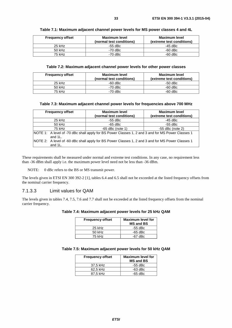
ETSI
ETSI EN 300 394-1 V3.3.1 (2015-04)33
Table 7.1: Maximum adjacent channel power levels for MS power classes 4 and 4L
Frequency offset Maximum level (normal test conditions)
Maximum level (extreme test conditions)
25 kHz -55 dBc -45 dBc 50 kHz -70 dBc -60 dBc 75 kHz -70 dBc -60 dBc
Table 7.2: Maximum adjacent channel power levels for other power classes
Frequency offset Maximum level (normal test conditions)
Maximum level (extreme test conditions)
25 kHz -60 dBc -50 dBc 50 kHz -70 dBc -60 dBc 75 kHz -70 dBc -60 dBc
Table 7.3: Maximum adjacent channel power levels for frequencies above 700 MHz
Frequency offset Maximum level (normal test conditions)
Maximum level (extreme test conditions)
25 kHz -55 dBc -45 dBc 50 kHz -65 dBc -55 dBc 75 kHz -65 dBc (note 1) -55 dBc (note 2)
NOTE 1: A level of -70 dBc shall apply for BS Power Classes 1, 2 and 3 and for MS Power Classes 1 and 1L.
NOTE 2: A level of -60 dBc shall apply for BS Power Classes 1, 2 and 3 and for MS Power Classes 1 and 1L.
These requirements shall be measured under normal and extreme test conditions. In any case, no requirement less than -36 dBm shall apply i.e. the maximum power level need not be less than -36 dBm.
NOTE: 0 dBc refers to the BS or MS transmit power.
The levels given in ETSI EN 300 392-2 [1], tables 6.4 and 6.5 shall not be exceeded at the listed frequency offsets from the nominal carrier frequency.
7.1.3.3 Limit values for QAM
The levels given in tables 7.4, 7.5, 7.6 and 7.7 shall not be exceeded at the listed frequency offsets from the nominal carrier frequency.
Table 7.4: Maximum adjacent power levels for 25 kHz QAM
Frequency offset Maximum level for MS and BS
25 kHz -55 dBc 50 kHz -65 dBc 75 kHz -67 dBc
Table 7.5: Maximum adjacent power levels for 50 kHz QAM
Frequency offset Maximum level for MS and BS
37,5 kHz -55 dBc 62,5 kHz -63 dBc 87,5 kHz -65 dBc
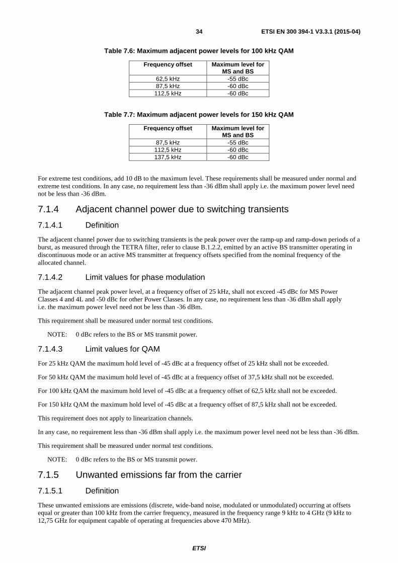
ETSI
ETSI EN 300 394-1 V3.3.1 (2015-04)34
Table 7.6: Maximum adjacent power levels for 100 kHz QAM
Frequency offset Maximum level for MS and BS
62,5 kHz -55 dBc 87,5 kHz -60 dBc
112,5 kHz -60 dBc
Table 7.7: Maximum adjacent power levels for 150 kHz QAM
Frequency offset Maximum level for MS and BS
87,5 kHz -55 dBc 112,5 kHz -60 dBc 137,5 kHz -60 dBc
For extreme test conditions, add 10 dB to the maximum level. These requirements shall be measured under normal and extreme test conditions. In any case, no requirement less than -36 dBm shall apply i.e. the maximum power level need not be less than -36 dBm.
7.1.4 Adjacent channel power due to switching transients
7.1.4.1 Definition
The adjacent channel power due to switching transients is the peak power over the ramp-up and ramp-down periods of a burst, as measured through the TETRA filter, refer to clause B.1.2.2, emitted by an active BS transmitter operating in discontinuous mode or an active MS transmitter at frequency offsets specified from the nominal frequency of the allocated channel.
7.1.4.2 Limit values for phase modulation
The adjacent channel peak power level, at a frequency offset of 25 kHz, shall not exceed -45 dBc for MS Power Classes 4 and 4L and -50 dBc for other Power Classes. In any case, no requirement less than -36 dBm shall apply i.e. the maximum power level need not be less than -36 dBm.
This requirement shall be measured under normal test conditions.
NOTE: 0 dBc refers to the BS or MS transmit power.
7.1.4.3 Limit values for QAM
For 25 kHz QAM the maximum hold level of -45 dBc at a frequency offset of 25 kHz shall not be exceeded.
For 50 kHz QAM the maximum hold level of -45 dBc at a frequency offset of 37,5 kHz shall not be exceeded.
For 100 kHz QAM the maximum hold level of -45 dBc at a frequency offset of 62,5 kHz shall not be exceeded.
For 150 kHz QAM the maximum hold level of -45 dBc at a frequency offset of 87,5 kHz shall not be exceeded.
This requirement does not apply to linearization channels.
In any case, no requirement less than -36 dBm shall apply i.e. the maximum power level need not be less than -36 dBm.
This requirement shall be measured under normal test conditions.
NOTE: 0 dBc refers to the BS or MS transmit power.
7.1.5 Unwanted emissions far from the carrier
7.1.5.1 Definition
These unwanted emissions are emissions (discrete, wide-band noise, modulated or unmodulated) occurring at offsets equal or greater than 100 kHz from the carrier frequency, measured in the frequency range 9 kHz to 4 GHz (9 kHz to 12,75 GHz for equipment capable of operating at frequencies above 470 MHz).
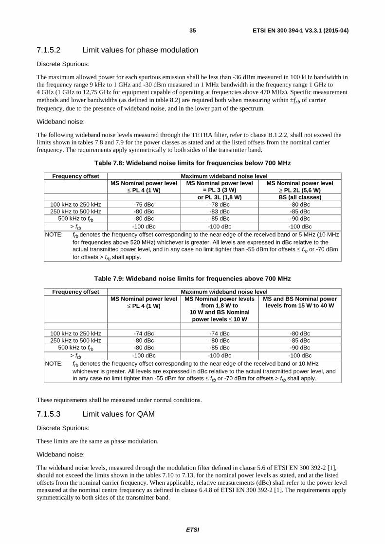
ETSI
ETSI EN 300 394-1 V3.3.1 (2015-04)35
7.1.5.2 Limit values for phase modulation
Discrete Spurious:
The maximum allowed power for each spurious emission shall be less than -36 dBm measured in 100 kHz bandwidth in the frequency range 9 kHz to 1 GHz and -30 dBm measured in 1 MHz bandwidth in the frequency range 1 GHz to 4 GHz (1 GHz to 12,75 GHz for equipment capable of operating at frequencies above 470 MHz). Specific measurement methods and lower bandwidths (as defined in table 8.2) are required both when measuring within ±frb of carrier frequency, due to the presence of wideband noise, and in the lower part of the spectrum.
Wideband noise:
The following wideband noise levels measured through the TETRA filter, refer to clause B.1.2.2, shall not exceed the limits shown in tables 7.8 and 7.9 for the power classes as stated and at the listed offsets from the nominal carrier frequency. The requirements apply symmetrically to both sides of the transmitter band.
Table 7.8: Wideband noise limits for frequencies below 700 MHz
Frequency offset Maximum wideband noise level MS Nominal power level
≤ PL 4 (1 W) MS Nominal power level
= PL 3 (3 W) MS Nominal power level
≥ PL 2L (5,6 W) or PL 3L (1,8 W) BS (all classes)
100 kHz to 250 kHz -75 dBc -78 dBc -80 dBc 250 kHz to 500 kHz -80 dBc -83 dBc -85 dBc
500 kHz to frb -80 dBc -85 dBc -90 dBc > frb -100 dBc -100 dBc -100 dBc
NOTE: frb denotes the frequency offset corresponding to the near edge of the received band or 5 MHz (10 MHz for frequencies above 520 MHz) whichever is greater. All levels are expressed in dBc relative to the actual transmitted power level, and in any case no limit tighter than -55 dBm for offsets ≤ frb or -70 dBm for offsets > frb shall apply.
Table 7.9: Wideband noise limits for frequencies above 700 MHz
Frequency offset Maximum wideband noise level MS Nominal power level
≤ PL 4 (1 W) MS Nominal power levels
from 1,8 W to 10 W and BS Nominal power levels ≤ 10 W
MS and BS Nominal power levels from 15 W to 40 W
100 kHz to 250 kHz -74 dBc -74 dBc -80 dBc 250 kHz to 500 kHz -80 dBc -80 dBc -85 dBc
500 kHz to frb -80 dBc -85 dBc -90 dBc > frb -100 dBc -100 dBc -100 dBc
NOTE: frb denotes the frequency offset corresponding to the near edge of the received band or 10 MHz whichever is greater. All levels are expressed in dBc relative to the actual transmitted power level, and in any case no limit tighter than -55 dBm for offsets ≤ frb or -70 dBm for offsets > frb shall apply.
These requirements shall be measured under normal conditions.
7.1.5.3 Limit values for QAM
Discrete Spurious:
These limits are the same as phase modulation.
Wideband noise:
The wideband noise levels, measured through the modulation filter defined in clause 5.6 of ETSI EN 300 392-2 [1], should not exceed the limits shown in the tables 7.10 to 7.13, for the nominal power levels as stated, and at the listed offsets from the nominal carrier frequency. When applicable, relative measurements (dBc) shall refer to the power level measured at the nominal centre frequency as defined in clause 6.4.8 of ETSI EN 300 392-2 [1]. The requirements apply symmetrically to both sides of the transmitter band.
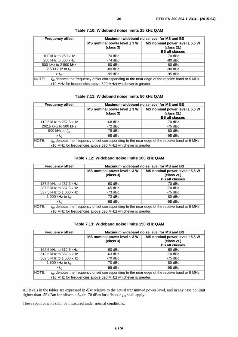
ETSI
ETSI EN 300 394-1 V3.3.1 (2015-04)36
Table 7.10: Wideband noise limits 25 kHz QAM
Frequency offset Maximum wideband noise level for MS and BS MS nominal power level ≤ 3 W
(class 3) MS nominal power level ≥ 5,6 W
(class 2L) BS all classes
100 kHz to 250 kHz -70 dBc -70 dBc 250 kHz to 500 kHz -74 dBc -80 dBc
500 kHz to 2 500 kHz -80 dBc -80 dBc 2 500 kHz to frb -80 dBc -90 dBc
> frb -95 dBc -95 dBc NOTE: frb denotes the frequency offset corresponding to the near edge of the receive band or 5 MHz
(10 MHz for frequencies above 520 MHz) whichever is greater.
Table 7.11: Wideband noise limits 50 kHz QAM
Frequency offset Maximum wideband noise level for MS and BS MS nominal power level ≤ 3 W
(class 3) MS nominal power level ≥ 5,6 W
(class 2L) BS all classes
112,5 kHz to 262,5 kHz -68 dBc -70 dBc 262,5 kHz to 500 kHz -72 dBc -75 dBc
500 kHz to frb -78 dBc -80 dBc > frb -95 dBc -95 dBc
NOTE: frb denotes the frequency offset corresponding to the near edge of the receive band or 5 MHz (10 MHz for frequencies above 520 MHz) whichever is greater.
Table 7.12: Wideband noise limits 100 kHz QAM
Frequency offset Maximum wideband noise level for MS and BS MS nominal power level ≤ 3 W
(class 3) MS nominal power level ≥ 5,6 W
(class 2L) BS all classes
137,5 kHz to 287,5 kHz -60 dBc -70 dBc 287,5 kHz to 537,5 kHz -65 dBc -70 dBc 537,5 kHz to 1 000 kHz -73 dBc -75 dBc
1 000 kHz to frb -73 dBc -80 dBc > frb -95 dBc -95 dBc
NOTE: frb denotes the frequency offset corresponding to the near edge of the receive band or 5 MHz (10 MHz for frequencies above 520 MHz) whichever is greater.
Table 7.13: Wideband noise limits 150 kHz QAM
Frequency offset Maximum wideband noise level for MS and BS MS nominal power level ≤ 3 W
(class 3) MS nominal power level ≥ 5,6 W
(class 2L) BS all classes
162,5 kHz to 312,5 kHz -60 dBc -60 dBc 312,5 kHz to 562,5 kHz -63 dBc -70 dBc 562,5 kHz to 1 500 kHz -70 dBc -75 dBc
1 500 kHz to frb -70 dBc -80 dBc > frb -95 dBc -95 dBc
NOTE: frb denotes the frequency offset corresponding to the near edge of the receive band or 5 MHz (10 MHz for frequencies above 520 MHz) whichever is greater.
All levels in the tables are expressed in dBc relative to the actual transmitted power level, and in any case no limit tighter than -55 dBm for offsets < frb or -70 dBm for offsets > frb shall apply.
These requirements shall be measured under normal conditions.
ETSI
ETSI EN 300 394-1 V3.3.1 (2015-04)37
7.1.6 Unwanted radiated emissions
7.1.6.1 Definition
Unwanted radiated emissions are emissions (whether modulated or unmodulated) radiated by the cabinet and structure of the equipment (MS or BS). This is also known as cabinet radiation.
7.1.6.2 Limit values
The limits given in clauses 7.1.5.2 (phase modulation) and 7.1.5.3 (QAM modulation) shall apply for frequencies between 30 MHz and 4 GHz only.
7.1.7 Unwanted emissions during the BLCH/CLCH (linearization)
7.1.7.1 Definition
These unwanted emissions are emissions produced by a BS or MS, measured through a TETRA filter, refer to clause B.1.2.2, at the specified frequency offset from the nominal carrier frequency, while the BS is transmitting a linearization burst on the BS Linearization Channel (BLCH) or a MS transmitting a linearization burst on the Common Linearization Channel (CLCH).
7.1.7.2 Limit values for phase modulation
The sum of the time periods during which the peak power, at a frequency offset of ±25 kHz during the BLCH/CLCH, is above -45 dBc shall not exceed 1 ms. This peak power shall never exceed -30 dBc.
NOTE: 0 dBc refers to the transmit power during normal operation after the BLCH/CLCH.
These requirements shall be measured under normal and extreme test conditions.
7.1.7.3 Limit values for QAM
For 25 kHz QAM the sum of the time periods during which the peak power, at a frequency offset of ±25 kHz during the BLCH-Q/CLCH-Q, is above -45 dBc shall not exceed 1 ms. This peak power shall never exceed -30 dBc.
For 50 kHz QAM the sum of the time periods during which the peak power, at a frequency offset of ±37,5 kHz during the BLCH-Q/CLCH-Q, is above -45 dBc shall not exceed 1 ms. This peak power shall never exceed -30 dBc.
For 100 kHz QAM the sum of the time periods during which the peak power, at a frequency offset of ±62,5 kHz during the BLCH-Q/CLCH-Q, is above -45 dBc shall not exceed 1 ms. This peak power shall never exceed -30 dBc.
For 150 kHz QAM the sum of the time periods during which the peak power, at a frequency offset of ±87,5 kHz during the BLCH-Q/CLCH-Q, is above -43 dBc shall not exceed 1 ms. This peak power shall never exceed -30 dBc.
NOTE: 0 dBc refers to the transmit power during normal operation after the CLCH-Q or BLCH-Q.
These requirements shall be measured under normal and extreme test conditions.
7.1.8 Transmitter intermodulation attenuation
7.1.8.1 Definition
Transmitter intermodulation attenuation is the ratio of the power level of the wanted signal to the power level of an intermodulation component. It is a measure of the capability of the transmitter to inhibit the generation of signals in its non-linear elements caused by the presence of the useful carrier and an interfering signal reaching the transmitter via its antenna.
ETSI
ETSI EN 300 394-1 V3.3.1 (2015-04)38
7.1.8.2 Limit values for phase modulation and QAM
7.1.8.2.1 MS Limit values
For an MS transmitter operating at the nominal power defined by its class, the intermodulation attenuation shall be at least 60 dB for any intermodulation component when measured in 30 kHz bandwidth. The interfering signal shall be unmodulated and have a frequency offset of at least 500 kHz from the carrier frequency. The power level of the interfering signal shall be 50 dB below the level of the modulated output signal from the transmitter under test.
This requirement shall be measured under normal test conditions.
7.1.8.2.2 Limit values for single BS transmitter
The intermodulation attenuation of the base station equipment shall be at least 70 dB for any intermodulation component when measured in 30 kHz bandwidth. However, in the case of base station equipment with only one transmitter and which is not intended to be collocated with other radio transmitting equipment, an intermodulation attenuation of at least 40 dB shall be sufficient. The interfering signal shall be unmodulated and have a frequency offset of at least 500 kHz from the carrier frequency. The power level of the interfering signal shall be 30 dB below the power level of the modulated output signal from the transmitter under test.
If the intermodulation attenuation is achieved by additional, internal or external, isolating devices they shall be included in the measurements.
In any case, no requirement less than -36 dBm shall apply i.e. the maximum power level need not be less than -36 dBm.
All power levels stated in the cases above are referring to the antenna connector of the base station.
These requirements shall be measured under normal test conditions.
7.1.8.2.3 Limit values for intra BS intermodulation
In a BS, intermodulation may be caused by combining several transmitters and carriers to feed a single antenna.
For all transmitters of a single TETRA base station, the power of any intermodulation components, when measured in a 30 kHz bandwidth, shall not exceed -60 dBc in the relevant downlink frequency band. In any case, no requirement less than -36 dBm shall apply i.e. the maximum power level need not be less than -36 dBm.
NOTE: The value of -60 dBc refers to the carrier power of the transmitter with the highest power output, measured at the antenna connector of the base station.
In the case where the performance is achieved by additional, internal or external isolating devices (such as circulators) they shall be supplied at the time of type testing and shall be used for measurements. The frequencies of the individual transmitters used during testing shall be stated in the test report.
This requirement shall be measured under normal test conditions.
7.2 Receiver parameter definitions and limits
7.2.1 General
The required minimum number of samples (bits in the case of BER measurements and messages in the case of MER and PUEM measurements) and the test limit error rates used in the following receiver tests have been defined such that:
a) the probability of passing a bad unit is lower than 0,3 %;
b) the probability of passing a good unit, operating on the limit of performance, is at least 99,5 %.
A unit shall be considered bad if its true BER/MER performance is worse than 1,5 times the specified BER/MER in static conditions and worse than 1,26 times the specified BER/MER in dynamic (fading multipath) conditions. These values have been adopted (taking into account the expected shapes of the BER/MER performance) in order to not to pass a unit with a sensitivity or interference rejection performance, 1 dB worse than that of a unit which just meets the specification.
NOTE: The above definition of a bad unit does not apply to PUEM measurements.

ETSI
ETSI EN 300 394-1 V3.3.1 (2015-04)39
Using at least the minimum number of samples shown in the tables of clause A.2, the MS or BS shall not exceed the test limits shown in the tables of clause A.2. These test limits (with the exception of PUEM measurements) are 1,22 times worse than the specified performance in static conditions, and 1,12 times worse than the specified performance in dynamic conditions, corresponding to a performance 0,5 dB worse than that specified. These values satisfy the requirements of a) and b) above. It is permitted to run the test over more samples than the value stated for minimum number of samples. The effect of increasing the number of samples is always to give a higher probability that a good unit will pass and a lower risk that a bad unit will pass, according to the definitions of good and bad unit in this clause.
All signal levels are referenced to the antenna connector of the equipment under test. The signal level is the available average power into 50 Ω measured over the useful part of a burst through the appropriate filter, refer to clause B.1.2.2.
7.2.2 Nominal error rates
7.2.2.1 Definition
The nominal error rate is a measure of the receiver performance under nominal channel conditions. Nominal channel conditions are defined as a received signal level ≥ -85 dBm with no interference under both static and fading conditions.
7.2.2.2 Limit values for phase modulation
The nominal bit error rate shall be measured. The cases to be tested and the corresponding limit values are given in the tables of clause A.2.
These requirements shall be measured under normal test conditions.
7.2.2.3 Limit values for QAM
The nominal bit error rate shall be measured. The cases to be tested and the corresponding limit values are given in the tables of clause A.2.
These requirements shall be measured under normal test conditions.
7.2.3 Reference sensitivity performance
7.2.3.1 Definition
The minimum required reference sensitivity performance is specified for V+D equipment according to test condition, logical channel, propagation condition, BS transmission mode, the receiver class, modulation type and channel bandwidth.
7.2.3.2 Limit values for phase modulation
The maximum dynamic and static reference sensitivity levels for a BS receiver under normal and extreme test conditions shall not exceed the signal levels shown in tables 7.14 and 7.15.
Table 7.14: BS receiver minimum reference sensitivity for π/4-DQPSK
Test condition Dynamic reference sensitivity Static reference sensitivity Normal -106 dBm -115 dBm Extreme -100 dBm -109 dBm
Table 7.15: BS receiver minimum reference sensitivity for π/8-D8PSK
Test condition Dynamic ref. Sensitivity Static reference sensitivity Normal -100 dBm -110 dBm Extreme -94 dBm -104 dBm
The maximum dynamic and static reference sensitivity levels for a MS receiver under normal and extreme test conditions shall not exceed the signal levels shown in tables 7.16 and 7.17.
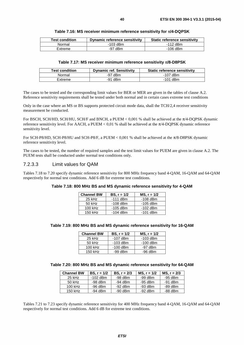
ETSI
ETSI EN 300 394-1 V3.3.1 (2015-04)40
Table 7.16: MS receiver minimum reference sensitivity for π/4-DQPSK
Test condition Dynamic reference sensitivity Static reference sensitivity Normal -103 dBm -112 dBm Extreme -97 dBm -106 dBm
Table 7.17: MS receiver minimum reference sensitivity π/8-D8PSK
Test condition Dynamic ref. Sensitivity Static reference sensitivity Normal -97 dBm -107 dBm Extreme -91 dBm -101 dBm
The cases to be tested and the corresponding limit values for BER or MER are given in the tables of clause A.2. Reference sensitivity requirements shall be tested under both normal and in certain cases extreme test conditions
Only in the case where an MS or BS supports protected circuit mode data, shall the TCH/2,4 receiver sensitivity measurement be conducted.
For BSCH, SCH/HD, SCH/HU, SCH/F and BNCH, a PUEM < 0,001 % shall be achieved at the π/4-DQPSK dynamic reference sensitivity level. For AACH, a PUEM < 0,01 % shall be achieved at the π/4-DQPSK dynamic reference sensitivity level.
For SCH-P8/HD, SCH-P8/HU and SCH-P8/F, a PUEM < 0,001 % shall be achieved at the π/8-D8PSK dynamic reference sensitivity level.
The cases to be tested, the number of required samples and the test limit values for PUEM are given in clause A.2. The PUEM tests shall be conducted under normal test conditions only.
7.2.3.3 Limit values for QAM
Tables 7.18 to 7.20 specify dynamic reference sensitivity for 800 MHz frequency band 4-QAM, 16-QAM and 64-QAM respectively for normal test conditions. Add 6 dB for extreme test conditions.
Table 7.18: 800 MHz BS and MS dynamic reference sensitivity for 4-QAM
Channel BW BS, r = 1/2 MS, r = 1/2 25 kHz -111 dBm -108 dBm 50 kHz -108 dBm -105 dBm
100 kHz -105 dBm -102 dBm 150 kHz -104 dBm -101 dBm
Table 7.19: 800 MHz BS and MS dynamic reference sensitivity for 16-QAM
Channel BW BS, r = 1/2 MS, r = 1/2 25 kHz -107 dBm -103 dBm 50 kHz -103 dBm -100 dBm
100 kHz -100 dBm -97 dBm 150 kHz -99 dBm -96 dBm
Table 7.20: 800 MHz BS and MS dynamic reference sensitivity for 64-QAM
Channel BW BS, r = 1/2 BS, r = 2/3 MS, r = 1/2 MS, r = 2/3 25 kHz -102 dBm -98 dBm -99 dBm -95 dBm 50 kHz -98 dBm -94 dBm -95 dBm -91 dBm
100 kHz -96 dBm -92 dBm -93 dBm -89 dBm 150 kHz -94 dBm -90 dBm -92 dBm -88 dBm
Tables 7.21 to 7.23 specify dynamic reference sensitivity for 400 MHz frequency band 4-QAM, 16-QAM and 64-QAM respectively for normal test conditions. Add 6 dB for extreme test conditions.

ETSI
ETSI EN 300 394-1 V3.3.1 (2015-04)41
Table 7.21: 400 MHz BS and MS dynamic reference sensitivity for 4-QAM
Channel BW BS, r = 1/2 MS, r = 1/2 25 kHz -111 dBm -108 dBm 50 kHz -108 dBm -105 dBm
100 kHz -105 dBm -102 dBm 150 kHz -104 dBm -101 dBm
Table 7.22: 400 MHz BS and MS dynamic reference sensitivity for 16-QAM
Channel BW BS, r = 1/2 MS, r = 1/2 25 kHz -106 dBm -103 dBm 50 kHz -102 dBm -100 dBm
100 kHz -100 dBm -97 dBm 150 kHz -99 dBm -96 dBm
Table 7.23: 400 MHz BS and MS dynamic reference sensitivity for 64-QAM
Channel BW
BS, r = 1/2 BS, r = 2/3 MS, r = 1/2 MS, r = 2/3
25 kHz -101 dBm -98 dBm -98 dBm -95 dBm 50 kHz -98 dBm -94 dBm -95 dBm -91 dBm
100 kHz -95 dBm -92 dBm -92 dBm -88 dBm 150 kHz -94 dBm -91 dBm -91 dBm -87 dBm
The minimum required static reference sensitivity performance for MS is specified in tables 7.24 and 7.25.
Table 7.24: QAM sensitivity levels for MS
Channel BW
4-QAM 3 % BER Sensitivity
16-QAM 3 % BER Sensitivity
64-QAM 3 % BER Sensitivity
25 kHz -113 dBm -106 dBm -101 dBm 50 kHz -110 dBm -103 dBm -97 dBm
100 kHz -107 dBm -100 dBm -95 dBm 150 kHz -105 dBm -99 dBm -93 dBm
The minimum required static reference sensitivity performance for BS is specified in the table 7.25.
Table 7.25: QAM sensitivity levels for BS
Channel BW
4-QAM 3 % BER Sensitivity
16-QAM 3 % BER Sensitivity
64-QAM 3 % BER Sensitivity
25 kHz -116 dBm -109 dBm -104 dBm 50 kHz -113 dBm -106 dBm -100 dBm
100 kHz -110 dBm -103 dBm -98 dBm 150 kHz -108 dBm -102 dBm -96 dBm
The cases to be tested and the corresponding limit values for BER or FER are given in the tables of clause A.2. Reference sensitivity requirements shall be tested under both normal and in certain cases extreme test conditions.
7.2.4 Reference interference performance
7.2.4.1 Definition
The minimum required reference interference performance (for co-channel C/Ic or adjacent channel C/Ia) is specified for V+D equipment with phase modulation according to test condition, channel type, propagation condition and the receiver class of the equipment.
The minimum required reference adjacent channel interference performance is specified for V+D equipment with QAM according to the wanted signal number of sub-carriers.
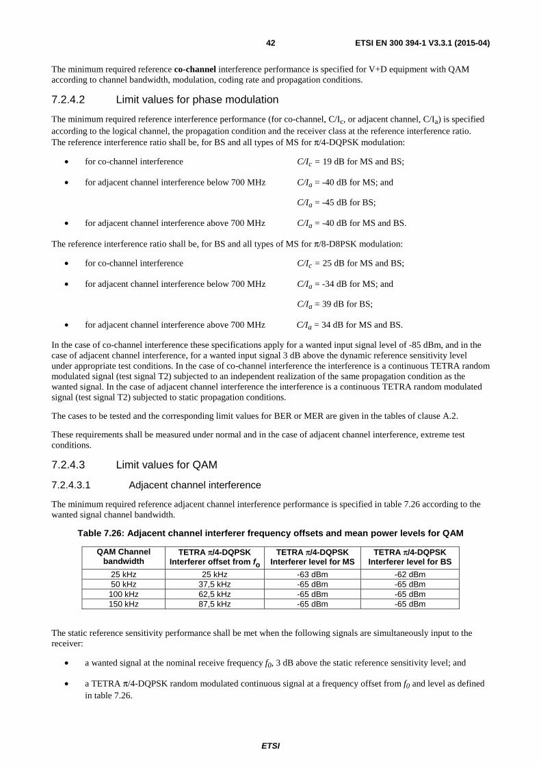
ETSI
ETSI EN 300 394-1 V3.3.1 (2015-04)42
The minimum required reference co-channel interference performance is specified for V+D equipment with QAM according to channel bandwidth, modulation, coding rate and propagation conditions.
7.2.4.2 Limit values for phase modulation
The minimum required reference interference performance (for co-channel, C/Ic, or adjacent channel, C/Ia) is specified according to the logical channel, the propagation condition and the receiver class at the reference interference ratio. The reference interference ratio shall be, for BS and all types of MS for π/4-DQPSK modulation:
• for co-channel interference C/Ic = 19 dB for MS and BS;
• for adjacent channel interference below 700 MHz C/Ia = -40 dB for MS; and
C/Ia = -45 dB for BS;
• for adjacent channel interference above 700 MHz C/Ia = -40 dB for MS and BS.
The reference interference ratio shall be, for BS and all types of MS for π/8-D8PSK modulation:
• for co-channel interference C/Ic = 25 dB for MS and BS;
• for adjacent channel interference below 700 MHz C/Ia = -34 dB for MS; and
C/Ia = 39 dB for BS;
• for adjacent channel interference above 700 MHz C/Ia = 34 dB for MS and BS.
In the case of co-channel interference these specifications apply for a wanted input signal level of -85 dBm, and in the case of adjacent channel interference, for a wanted input signal 3 dB above the dynamic reference sensitivity level under appropriate test conditions. In the case of co-channel interference the interference is a continuous TETRA random modulated signal (test signal T2) subjected to an independent realization of the same propagation condition as the wanted signal. In the case of adjacent channel interference the interference is a continuous TETRA random modulated signal (test signal T2) subjected to static propagation conditions.
The cases to be tested and the corresponding limit values for BER or MER are given in the tables of clause A.2.
These requirements shall be measured under normal and in the case of adjacent channel interference, extreme test conditions.
7.2.4.3 Limit values for QAM
7.2.4.3.1 Adjacent channel interference
The minimum required reference adjacent channel interference performance is specified in table 7.26 according to the wanted signal channel bandwidth.
Table 7.26: Adjacent channel interferer frequency offsets and mean power levels for QAM
QAM Channel bandwidth
TETRA π/4-DQPSK Interferer offset from fo
TETRA π/4-DQPSK Interferer level for MS
TETRA π/4-DQPSK Interferer level for BS
25 kHz 25 kHz -63 dBm -62 dBm 50 kHz 37,5 kHz -65 dBm -65 dBm
100 kHz 62,5 kHz -65 dBm -65 dBm 150 kHz 87,5 kHz -65 dBm -65 dBm
The static reference sensitivity performance shall be met when the following signals are simultaneously input to the receiver:
• a wanted signal at the nominal receive frequency f0, 3 dB above the static reference sensitivity level; and
• a TETRA π/4-DQPSK random modulated continuous signal at a frequency offset from f0 and level as defined in table 7.26.
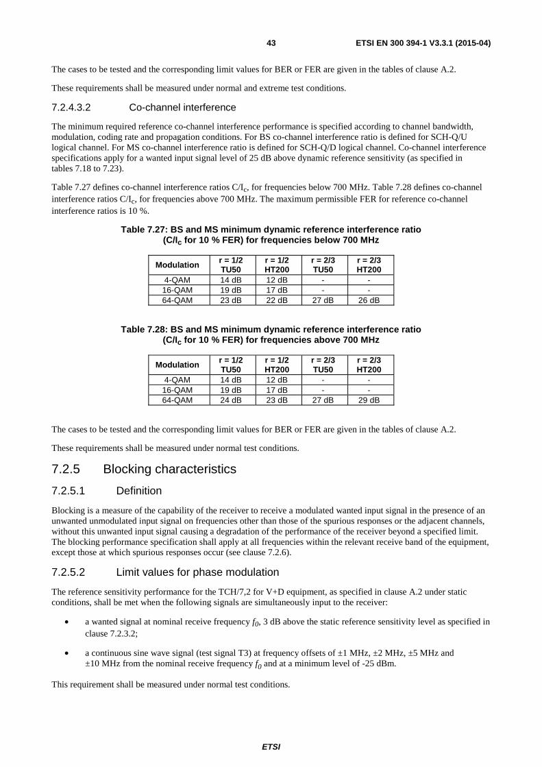
ETSI
ETSI EN 300 394-1 V3.3.1 (2015-04)43
The cases to be tested and the corresponding limit values for BER or FER are given in the tables of clause A.2.
These requirements shall be measured under normal and extreme test conditions.
7.2.4.3.2 Co-channel interference
The minimum required reference co-channel interference performance is specified according to channel bandwidth, modulation, coding rate and propagation conditions. For BS co-channel interference ratio is defined for SCH-Q/U logical channel. For MS co-channel interference ratio is defined for SCH-Q/D logical channel. Co-channel interference specifications apply for a wanted input signal level of 25 dB above dynamic reference sensitivity (as specified in tables 7.18 to 7.23).
Table 7.27 defines co-channel interference ratios C/Ic, for frequencies below 700 MHz. Table 7.28 defines co-channel interference ratios C/Ic, for frequencies above 700 MHz. The maximum permissible FER for reference co-channel interference ratios is 10 %.
Table 7.27: BS and MS minimum dynamic reference interference ratio (C/Ic for 10 % FER) for frequencies below 700 MHz
Modulation r = 1/2 TU50
r = 1/2 HT200
r = 2/3 TU50
r = 2/3 HT200
4-QAM 14 dB 12 dB - - 16-QAM 19 dB 17 dB - - 64-QAM 23 dB 22 dB 27 dB 26 dB
Table 7.28: BS and MS minimum dynamic reference interference ratio (C/Ic for 10 % FER) for frequencies above 700 MHz
Modulation r = 1/2 TU50
r = 1/2 HT200
r = 2/3 TU50
r = 2/3 HT200
4-QAM 14 dB 12 dB - - 16-QAM 19 dB 17 dB - - 64-QAM 24 dB 23 dB 27 dB 29 dB
The cases to be tested and the corresponding limit values for BER or FER are given in the tables of clause A.2.
These requirements shall be measured under normal test conditions.
7.2.5 Blocking characteristics
7.2.5.1 Definition
Blocking is a measure of the capability of the receiver to receive a modulated wanted input signal in the presence of an unwanted unmodulated input signal on frequencies other than those of the spurious responses or the adjacent channels, without this unwanted input signal causing a degradation of the performance of the receiver beyond a specified limit. The blocking performance specification shall apply at all frequencies within the relevant receive band of the equipment, except those at which spurious responses occur (see clause 7.2.6).
7.2.5.2 Limit values for phase modulation
The reference sensitivity performance for the TCH/7,2 for V+D equipment, as specified in clause A.2 under static conditions, shall be met when the following signals are simultaneously input to the receiver:
• a wanted signal at nominal receive frequency f0, 3 dB above the static reference sensitivity level as specified in clause 7.2.3.2;
• a continuous sine wave signal (test signal T3) at frequency offsets of ±1 MHz, ±2 MHz, ±5 MHz and ±10 MHz from the nominal receive frequency f0 and at a minimum level of -25 dBm.
This requirement shall be measured under normal test conditions.
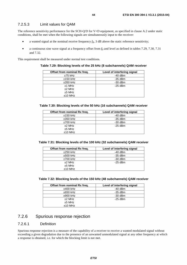
ETSI
ETSI EN 300 394-1 V3.3.1 (2015-04)44
7.2.5.3 Limit values for QAM
The reference sensitivity performance for the SCH-Q/D for V+D equipment, as specified in clause A.2 under static conditions, shall be met when the following signals are simultaneously input to the receiver:
• a wanted signal at the nominal receive frequency f0, 3 dB above the static reference sensitivity;
• a continuous sine wave signal at a frequency offset from f0 and level as defined in tables 7.29, 7.30, 7.31 and 7.32.
This requirement shall be measured under normal test conditions.
Table 7.29: Blocking levels of the 25 kHz (8 subchannels) QAM receiver
Offset from nominal Rx freq. Level of interfering signal ±75 kHz -40 dBm
±150 kHz -35 dBm ±350 kHz -30 dBm ±1 MHz ±2 MHz ±5 MHz
±10 MHz
-25 dBm
Table 7.30: Blocking levels of the 50 kHz (16 subchannels) QAM receiver
Offset from nominal Rx freq. Level of interfering signal ±150 kHz -40 dBm ±350 kHz -35 dBm ±700 kHz -30 dBm ±2 MHz ±5 MHz
±10 MHz
-25 dBm
Table 7.31: Blocking levels of the 100 kHz (32 subchannels) QAM receiver
Offset from nominal Rx freq. Level of interfering signal ±250 kHz -40 dBm ±500 kHz -35 dBm ±700 kHz -30 dBm ±2 MHz ±5 MHz
±10 MHz
-25 dBm
Table 7.32: Blocking levels of the 150 kHz (48 subchannels) QAM receiver
Offset from nominal Rx freq. Level of interfering signal ±400 kHz -40 dBm ±650 kHz -35 dBm ±900 kHz -30 dBm ±2 MHz ±5 MHz
±10 MHz
-25 dBm
7.2.6 Spurious response rejection
7.2.6.1 Definition
Spurious response rejection is a measure of the capability of a receiver to receive a wanted modulated signal without exceeding a given degradation due to the presence of an unwanted unmodulated signal at any other frequency at which a response is obtained, i.e. for which the blocking limit is not met.
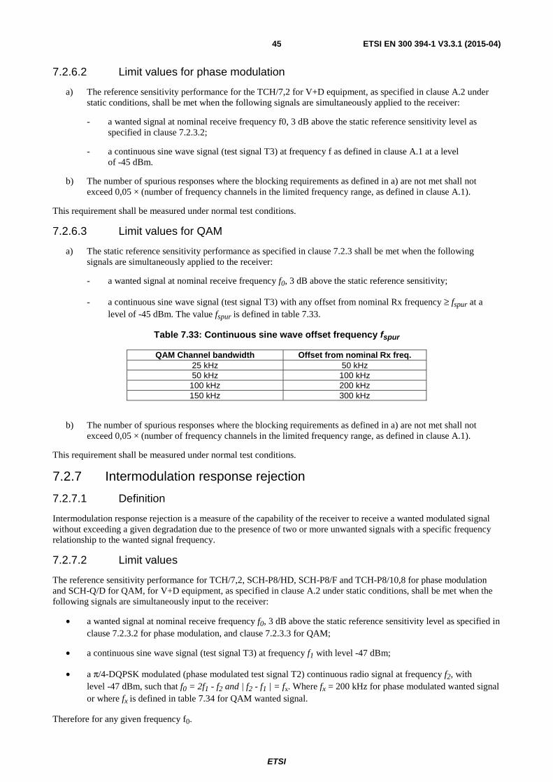
ETSI
ETSI EN 300 394-1 V3.3.1 (2015-04)45
7.2.6.2 Limit values for phase modulation
a) The reference sensitivity performance for the TCH/7,2 for V+D equipment, as specified in clause A.2 under static conditions, shall be met when the following signals are simultaneously applied to the receiver:
- a wanted signal at nominal receive frequency f0, 3 dB above the static reference sensitivity level as specified in clause 7.2.3.2;
- a continuous sine wave signal (test signal T3) at frequency f as defined in clause A.1 at a level of -45 dBm.
b) The number of spurious responses where the blocking requirements as defined in a) are not met shall not exceed 0,05 × (number of frequency channels in the limited frequency range, as defined in clause A.1).
This requirement shall be measured under normal test conditions.
7.2.6.3 Limit values for QAM
a) The static reference sensitivity performance as specified in clause 7.2.3 shall be met when the following signals are simultaneously applied to the receiver:
- a wanted signal at nominal receive frequency f0, 3 dB above the static reference sensitivity;
- a continuous sine wave signal (test signal T3) with any offset from nominal Rx frequency ≥ fspur at a level of -45 dBm. The value fspur is defined in table 7.33.
Table 7.33: Continuous sine wave offset frequency fspur
QAM Channel bandwidth Offset from nominal Rx freq. 25 kHz 50 kHz 50 kHz 100 kHz
100 kHz 200 kHz 150 kHz 300 kHz
b) The number of spurious responses where the blocking requirements as defined in a) are not met shall not exceed 0,05 × (number of frequency channels in the limited frequency range, as defined in clause A.1).
This requirement shall be measured under normal test conditions.
7.2.7 Intermodulation response rejection
7.2.7.1 Definition
Intermodulation response rejection is a measure of the capability of the receiver to receive a wanted modulated signal without exceeding a given degradation due to the presence of two or more unwanted signals with a specific frequency relationship to the wanted signal frequency.
7.2.7.2 Limit values
The reference sensitivity performance for TCH/7,2, SCH-P8/HD, SCH-P8/F and TCH-P8/10,8 for phase modulation and SCH-Q/D for QAM, for V+D equipment, as specified in clause A.2 under static conditions, shall be met when the following signals are simultaneously input to the receiver:
• a wanted signal at nominal receive frequency f0, 3 dB above the static reference sensitivity level as specified in clause 7.2.3.2 for phase modulation, and clause 7.2.3.3 for QAM;
• a continuous sine wave signal (test signal T3) at frequency f1 with level -47 dBm;
• a π/4-DQPSK modulated (phase modulated test signal T2) continuous radio signal at frequency f2, with level -47 dBm, such that f0 = 2f1 - f2 and | f2 - f1 | = fx. Where fx = 200 kHz for phase modulated wanted signal or where fx is defined in table 7.34 for QAM wanted signal.
Therefore for any given frequency f0.
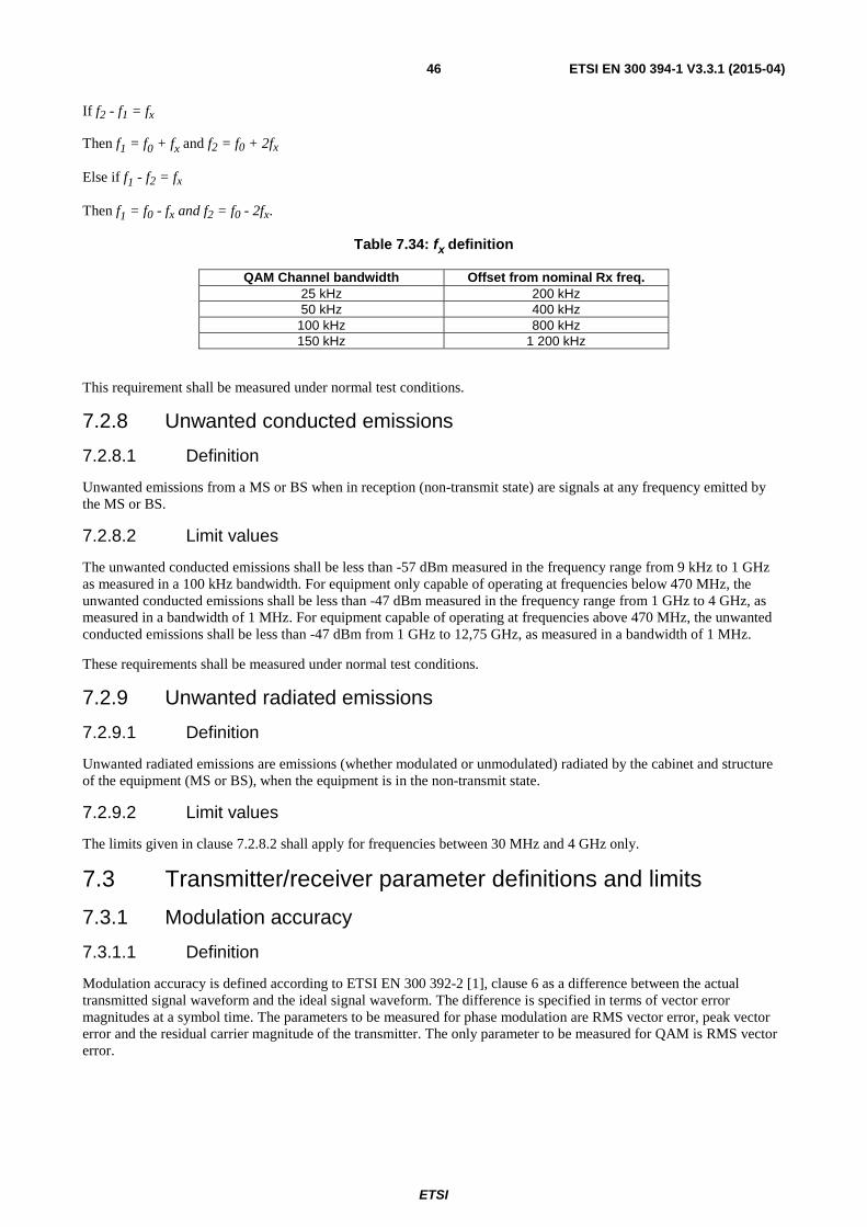
ETSI
ETSI EN 300 394-1 V3.3.1 (2015-04)46
If f2 - f1 = fx
Then f1 = f0 + fx and f2 = f0 + 2fx
Else if f1 - f2 = fx
Then f1 = f0 - fx and f2 = f0 - 2fx.
Table 7.34: fx definition
QAM Channel bandwidth Offset from nominal Rx freq. 25 kHz 200 kHz 50 kHz 400 kHz
100 kHz 800 kHz 150 kHz 1 200 kHz
This requirement shall be measured under normal test conditions.
7.2.8 Unwanted conducted emissions
7.2.8.1 Definition
Unwanted emissions from a MS or BS when in reception (non-transmit state) are signals at any frequency emitted by the MS or BS.
7.2.8.2 Limit values
The unwanted conducted emissions shall be less than -57 dBm measured in the frequency range from 9 kHz to 1 GHz as measured in a 100 kHz bandwidth. For equipment only capable of operating at frequencies below 470 MHz, the unwanted conducted emissions shall be less than -47 dBm measured in the frequency range from 1 GHz to 4 GHz, as measured in a bandwidth of 1 MHz. For equipment capable of operating at frequencies above 470 MHz, the unwanted conducted emissions shall be less than -47 dBm from 1 GHz to 12,75 GHz, as measured in a bandwidth of 1 MHz.
These requirements shall be measured under normal test conditions.
7.2.9 Unwanted radiated emissions
7.2.9.1 Definition
Unwanted radiated emissions are emissions (whether modulated or unmodulated) radiated by the cabinet and structure of the equipment (MS or BS), when the equipment is in the non-transmit state.
7.2.9.2 Limit values
The limits given in clause 7.2.8.2 shall apply for frequencies between 30 MHz and 4 GHz only.
7.3 Transmitter/receiver parameter definitions and limits
7.3.1 Modulation accuracy
7.3.1.1 Definition
Modulation accuracy is defined according to ETSI EN 300 392-2 [1], clause 6 as a difference between the actual transmitted signal waveform and the ideal signal waveform. The difference is specified in terms of vector error magnitudes at a symbol time. The parameters to be measured for phase modulation are RMS vector error, peak vector error and the residual carrier magnitude of the transmitter. The only parameter to be measured for QAM is RMS vector error.
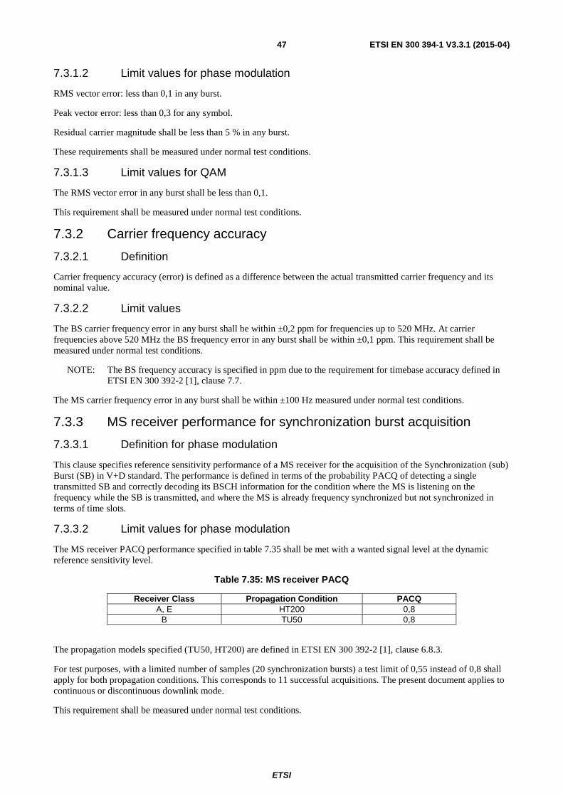
ETSI
ETSI EN 300 394-1 V3.3.1 (2015-04)47
7.3.1.2 Limit values for phase modulation
RMS vector error: less than 0,1 in any burst.
Peak vector error: less than 0,3 for any symbol.
Residual carrier magnitude shall be less than 5 % in any burst.
These requirements shall be measured under normal test conditions.
7.3.1.3 Limit values for QAM
The RMS vector error in any burst shall be less than 0,1.
This requirement shall be measured under normal test conditions.
7.3.2 Carrier frequency accuracy
7.3.2.1 Definition
Carrier frequency accuracy (error) is defined as a difference between the actual transmitted carrier frequency and its nominal value.
7.3.2.2 Limit values
The BS carrier frequency error in any burst shall be within ±0,2 ppm for frequencies up to 520 MHz. At carrier frequencies above 520 MHz the BS frequency error in any burst shall be within ±0,1 ppm. This requirement shall be measured under normal test conditions.
NOTE: The BS frequency accuracy is specified in ppm due to the requirement for timebase accuracy defined in ETSI EN 300 392-2 [1], clause 7.7.
The MS carrier frequency error in any burst shall be within ±100 Hz measured under normal test conditions.
7.3.3 MS receiver performance for synchronization burst acquisition
7.3.3.1 Definition for phase modulation
This clause specifies reference sensitivity performance of a MS receiver for the acquisition of the Synchronization (sub) Burst (SB) in V+D standard. The performance is defined in terms of the probability PACQ of detecting a single transmitted SB and correctly decoding its BSCH information for the condition where the MS is listening on the frequency while the SB is transmitted, and where the MS is already frequency synchronized but not synchronized in terms of time slots.
7.3.3.2 Limit values for phase modulation
The MS receiver PACQ performance specified in table 7.35 shall be met with a wanted signal level at the dynamic reference sensitivity level.
Table 7.35: MS receiver PACQ
Receiver Class Propagation Condition PACQ A, E HT200 0,8
B TU50 0,8
The propagation models specified (TU50, HT200) are defined in ETSI EN 300 392-2 [1], clause 6.8.3.
For test purposes, with a limited number of samples (20 synchronization bursts) a test limit of 0,55 instead of 0,8 shall apply for both propagation conditions. This corresponds to 11 successful acquisitions. The present document applies to continuous or discontinuous downlink mode.
This requirement shall be measured under normal test conditions.
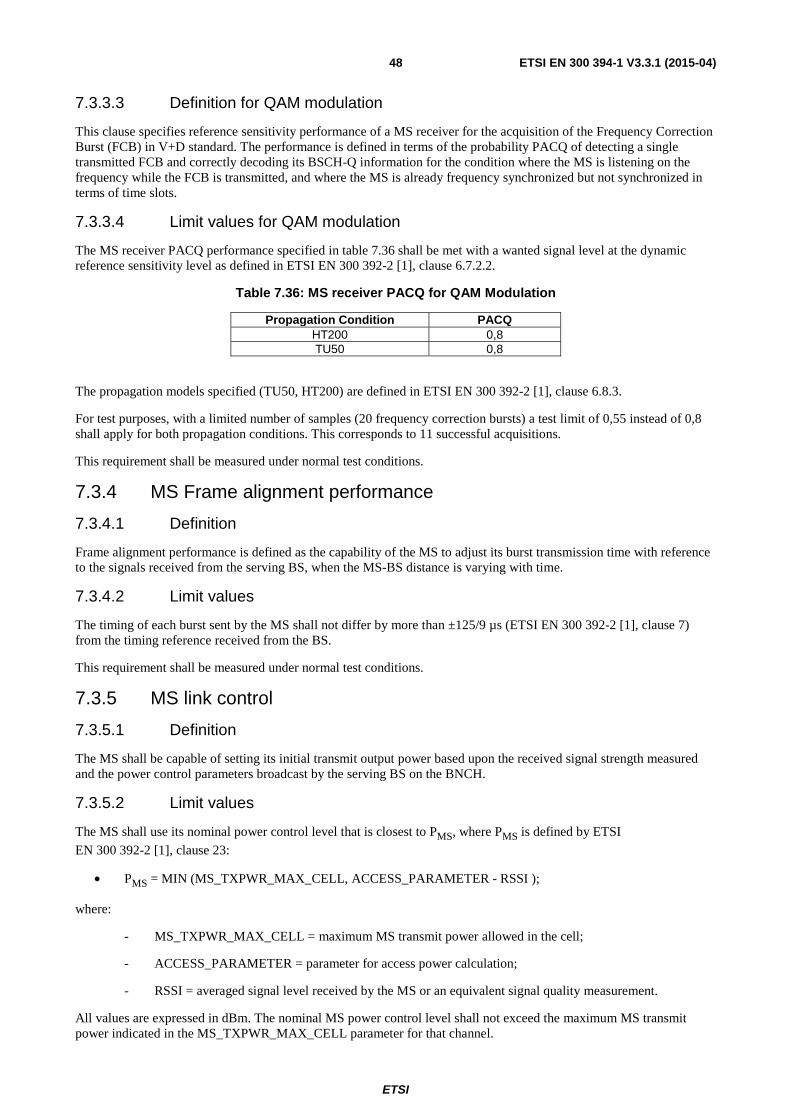
ETSI
ETSI EN 300 394-1 V3.3.1 (2015-04)48
7.3.3.3 Definition for QAM modulation
This clause specifies reference sensitivity performance of a MS receiver for the acquisition of the Frequency Correction Burst (FCB) in V+D standard. The performance is defined in terms of the probability PACQ of detecting a single transmitted FCB and correctly decoding its BSCH-Q information for the condition where the MS is listening on the frequency while the FCB is transmitted, and where the MS is already frequency synchronized but not synchronized in terms of time slots.
7.3.3.4 Limit values for QAM modulation
The MS receiver PACQ performance specified in table 7.36 shall be met with a wanted signal level at the dynamic reference sensitivity level as defined in ETSI EN 300 392-2 [1], clause 6.7.2.2.
Table 7.36: MS receiver PACQ for QAM Modulation
Propagation Condition PACQ HT200 0,8 TU50 0,8
The propagation models specified (TU50, HT200) are defined in ETSI EN 300 392-2 [1], clause 6.8.3.
For test purposes, with a limited number of samples (20 frequency correction bursts) a test limit of 0,55 instead of 0,8 shall apply for both propagation conditions. This corresponds to 11 successful acquisitions.
This requirement shall be measured under normal test conditions.
7.3.4 MS Frame alignment performance
7.3.4.1 Definition
Frame alignment performance is defined as the capability of the MS to adjust its burst transmission time with reference to the signals received from the serving BS, when the MS-BS distance is varying with time.
7.3.4.2 Limit values
The timing of each burst sent by the MS shall not differ by more than ±125/9 µs (ETSI EN 300 392-2 [1], clause 7) from the timing reference received from the BS.
This requirement shall be measured under normal test conditions.
7.3.5 MS link control
7.3.5.1 Definition
The MS shall be capable of setting its initial transmit output power based upon the received signal strength measured and the power control parameters broadcast by the serving BS on the BNCH.
7.3.5.2 Limit values
The MS shall use its nominal power control level that is closest to PMS, where PMS is defined by ETSI
EN 300 392-2 [1], clause 23:
• PMS = MIN (MS_TXPWR_MAX_CELL, ACCESS_PARAMETER - RSSI );
where:
- MS_TXPWR_MAX_CELL = maximum MS transmit power allowed in the cell;
- ACCESS_PARAMETER = parameter for access power calculation;
- RSSI = averaged signal level received by the MS or an equivalent signal quality measurement.
All values are expressed in dBm. The nominal MS power control level shall not exceed the maximum MS transmit power indicated in the MS_TXPWR_MAX_CELL parameter for that channel.
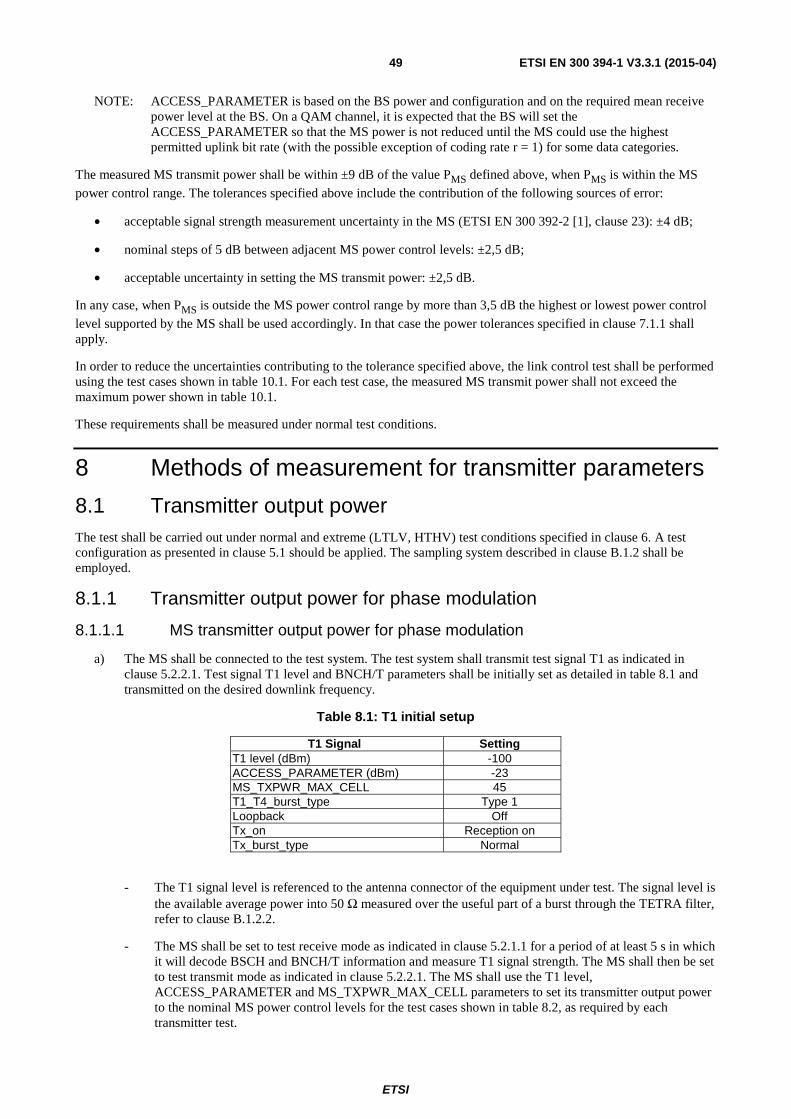
ETSI
ETSI EN 300 394-1 V3.3.1 (2015-04)49
NOTE: ACCESS_PARAMETER is based on the BS power and configuration and on the required mean receive power level at the BS. On a QAM channel, it is expected that the BS will set the ACCESS_PARAMETER so that the MS power is not reduced until the MS could use the highest permitted uplink bit rate (with the possible exception of coding rate r = 1) for some data categories.
The measured MS transmit power shall be within ±9 dB of the value PMS defined above, when PMS is within the MS
power control range. The tolerances specified above include the contribution of the following sources of error:
• acceptable signal strength measurement uncertainty in the MS (ETSI EN 300 392-2 [1], clause 23): ±4 dB;
• nominal steps of 5 dB between adjacent MS power control levels: ±2,5 dB;
• acceptable uncertainty in setting the MS transmit power: ±2,5 dB.
In any case, when PMS is outside the MS power control range by more than 3,5 dB the highest or lowest power control
level supported by the MS shall be used accordingly. In that case the power tolerances specified in clause 7.1.1 shall apply.
In order to reduce the uncertainties contributing to the tolerance specified above, the link control test shall be performed using the test cases shown in table 10.1. For each test case, the measured MS transmit power shall not exceed the maximum power shown in table 10.1.
These requirements shall be measured under normal test conditions.
8 Methods of measurement for transmitter parameters
8.1 Transmitter output power The test shall be carried out under normal and extreme (LTLV, HTHV) test conditions specified in clause 6. A test configuration as presented in clause 5.1 should be applied. The sampling system described in clause B.1.2 shall be employed.
8.1.1 Transmitter output power for phase modulation
8.1.1.1 MS transmitter output power for phase modulation
a) The MS shall be connected to the test system. The test system shall transmit test signal T1 as indicated in clause 5.2.2.1. Test signal T1 level and BNCH/T parameters shall be initially set as detailed in table 8.1 and transmitted on the desired downlink frequency.
Table 8.1: T1 initial setup
T1 Signal Setting T1 level (dBm) -100 ACCESS_PARAMETER (dBm) -23 MS_TXPWR_MAX_CELL 45 T1_T4_burst_type Type 1 Loopback Off Tx_on Reception on Tx_burst_type Normal
- The T1 signal level is referenced to the antenna connector of the equipment under test. The signal level is the available average power into 50 Ω measured over the useful part of a burst through the TETRA filter, refer to clause B.1.2.2.
- The MS shall be set to test receive mode as indicated in clause 5.2.1.1 for a period of at least 5 s in which it will decode BSCH and BNCH/T information and measure T1 signal strength. The MS shall then be set to test transmit mode as indicated in clause 5.2.2.1. The MS shall use the T1 level, ACCESS_PARAMETER and MS_TXPWR_MAX_CELL parameters to set its transmitter output power to the nominal MS power control levels for the test cases shown in table 8.2, as required by each transmitter test.
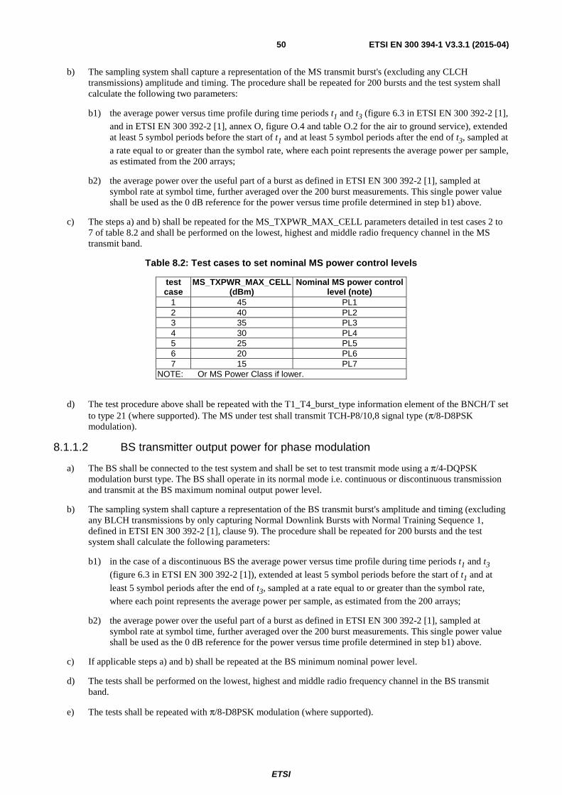
ETSI
ETSI EN 300 394-1 V3.3.1 (2015-04)50
b) The sampling system shall capture a representation of the MS transmit burst's (excluding any CLCH transmissions) amplitude and timing. The procedure shall be repeated for 200 bursts and the test system shall calculate the following two parameters:
b1) the average power versus time profile during time periods t1 and t3 (figure 6.3 in ETSI EN 300 392-2 [1],
and in ETSI EN 300 392-2 [1], annex O, figure O.4 and table O.2 for the air to ground service), extended at least 5 symbol periods before the start of t1 and at least 5 symbol periods after the end of t3, sampled at
a rate equal to or greater than the symbol rate, where each point represents the average power per sample, as estimated from the 200 arrays;
b2) the average power over the useful part of a burst as defined in ETSI EN 300 392-2 [1], sampled at symbol rate at symbol time, further averaged over the 200 burst measurements. This single power value shall be used as the 0 dB reference for the power versus time profile determined in step b1) above.
c) The steps a) and b) shall be repeated for the MS_TXPWR_MAX_CELL parameters detailed in test cases 2 to 7 of table 8.2 and shall be performed on the lowest, highest and middle radio frequency channel in the MS transmit band.
Table 8.2: Test cases to set nominal MS power control levels
test case
MS_TXPWR_MAX_CELL (dBm)
Nominal MS power control level (note)
1 45 PL1 2 40 PL2 3 35 PL3 4 30 PL4 5 25 PL5 6 20 PL6 7 15 PL7
NOTE: Or MS Power Class if lower.
d) The test procedure above shall be repeated with the T1_T4_burst_type information element of the BNCH/T set to type 21 (where supported). The MS under test shall transmit TCH-P8/10,8 signal type (π/8-D8PSK modulation).
8.1.1.2 BS transmitter output power for phase modulation
a) The BS shall be connected to the test system and shall be set to test transmit mode using a π/4-DQPSK modulation burst type. The BS shall operate in its normal mode i.e. continuous or discontinuous transmission and transmit at the BS maximum nominal output power level.
b) The sampling system shall capture a representation of the BS transmit burst's amplitude and timing (excluding any BLCH transmissions by only capturing Normal Downlink Bursts with Normal Training Sequence 1, defined in ETSI EN 300 392-2 [1], clause 9). The procedure shall be repeated for 200 bursts and the test system shall calculate the following parameters:
b1) in the case of a discontinuous BS the average power versus time profile during time periods t1 and t3
(figure 6.3 in ETSI EN 300 392-2 [1]), extended at least 5 symbol periods before the start of t1 and at
least 5 symbol periods after the end of t3, sampled at a rate equal to or greater than the symbol rate,
where each point represents the average power per sample, as estimated from the 200 arrays;
b2) the average power over the useful part of a burst as defined in ETSI EN 300 392-2 [1], sampled at symbol rate at symbol time, further averaged over the 200 burst measurements. This single power value shall be used as the 0 dB reference for the power versus time profile determined in step b1) above.
c) If applicable steps a) and b) shall be repeated at the BS minimum nominal power level.
d) The tests shall be performed on the lowest, highest and middle radio frequency channel in the BS transmit band.
e) The tests shall be repeated with π/8-D8PSK modulation (where supported).

ETSI
ETSI EN 300 394-1 V3.3.1 (2015-04)51
8.1.2 Transmitter output power for QAM
8.1.2.1 MS transmitter output power for QAM
a) The MS shall be connected to the test system. The test system shall transmit the QAM test signal T4 as indicated in clause 5.2.2.2. continuously with channel type 27. The test signal level and BNCH/T parameters shall be initially set as detailed in table 8.3 and transmitted on the desired downlink frequency.
Table 8.3: T4 initial setup
T4 Signal Setting T4 level (dBm) -100 ACCESS_PARAMETER (dBm) -23 MS_TXPWR_MAX_CELL 45 burst_type Type 27 Loopback Off Tx_on Reception on Tx_burst_type Normal Error correction 0 Bandwidth of QAM channel 25
- The T4 signal level is referenced to the antenna connector of the equipment under test. The signal level is the available average power into 50 Ω measured over the useful part of a burst.
- The MS shall be set to test receive mode as indicated in clause 5.2.1.3 for a period of at least 5 s in which it will decode BSCH and BNCH/T information and measure T4 signal strength. The MS shall then be set to test transmit mode as indicated in clause 5.2.2.2. The MS shall use the T4 level, ACCESS_PARAMETER and MS_TXPWR_MAX_CELL parameters to set its transmitter output power to the nominal MS power control levels for the test cases shown in table 8.2, as required by each transmitter test.
b) The sampling system shall capture a representation of the MS transmit burst's (excluding any CLCH transmissions) amplitude and timing. The procedure shall be repeated for 200 bursts and the test system shall calculate the following parameters:
b1) the average power versus time profile during time periods t1 and t3 (figure 6.4 in ETSI
EN 300 392-2 [1]), extended at least 2 symbol periods before the start of t1 and at least 2 symbol periods
after the end of t3, sampled at a rate equal to or greater than the symbol rate, where each point represents
the average power per sample, as estimated from the 200 arrays;
b2) the average power over the useful part of a burst as defined in ETSI EN 300 392-2 [1]. This is the sum of the powers of each of the sub-carriers within the RF channel bandwidth. For each sub-carrier, reference power is the average power, measured at symbol time through the square root raised cosine filter defined in ETSI EN 300 392-2 [1], clause 5.16, over the pilot and sync symbols within the QAM burst, further averaged over the 200 burst measurements. The average power value shall be used as the 0 dB reference for the power versus time profile determined in step b1) above;
b3) each individual pilot sub-carrier symbol power. This shall be measured to compare with the reference power from that sub-carrier.
c) The steps a) and b) shall be repeated for the MS_TXPWR_MAX_CELL parameters detailed in test cases 1 to 7 of table 8.2 and shall be performed on the lowest, highest and middle radio frequency channel in the MS transmit band.
d) This test shall be performed (where supported) using 4-QAM, 16-QAM, and 64-QAM modulation and at 25 kHz, 50 kHz, 100 kHz, and 150 kHz channel bandwidths.
ETSI
ETSI EN 300 394-1 V3.3.1 (2015-04)52
8.1.2.2 BS transmitter output power for QAM
a) The BS shall be connected to the test system and shall be set to test transmit mode using a QAM normal downlink burst type. The BS shall transmit at the BS maximum nominal output power level.
b) The sampling system shall capture a representation of the BS transmit burst's amplitude and timing (excluding any linearization down-link burst transmissions by only capturing Normal Downlink Bursts, defined in ETSI EN 300 392-2 [1], clause 9). The procedure shall be repeated for 200 bursts and the test system shall calculate the following parameters:
b1) the average power over the useful part of a burst as defined in ETSI EN 300 392-2 [1]. This shall be defined as the sum of the powers of each of the sub-carriers within the RF channel bandwidth. For each sub-carrier, reference power is defined as the average power, measured at symbol time through the square root raised cosine filter, over the pilot and sync symbols within the QAM, further averaged over the 200 burst measurements;
b2) each individual pilot sub-carrier symbol power. This shall be measured to compare with the reference power from that sub-carrier.
c) If applicable steps a) and b) shall be repeated at the BS minimum nominal power level.
d) This test shall be performed (where supported) using 4-QAM, 16-QAM, and 64-QAM modulation and at 25 kHz, 50 kHz, 100 kHz, and 150 kHz channel bandwidths.
8.2 Unwanted output power in non active transmit state The test shall be carried out at maximum nominal power level only under the normal test conditions specified in clause 6.
The procedure detailed in clauses 8.1.1.1 a) and 8.1.2.1 a) for MS or clause 8.1.1.2 a) for discontinuous BS shall be used. The sampling system shall be used to measure the average unwanted transmitter output power during the non-active time slots occurring between the successive burst transmissions of the MS or BS operating in discontinuous mode. The equipment under test shall transmit a burst only in one timeslot per frame and, hence each transmitted burst is followed by three non-active time slots.
The test system shall calculate the average power over 200 non active time slots by applying the measurement procedure detailed in step b2) of clause 8.1.1.1 or clause 8.1.2.1 for MS and clause 8.1.1.2 for discontinuous BS to the active time slots, and by continuing to sample at a rate equal to or greater than the symbol rate during the whole non-active period of the non active time slots. The transmitter output power measured during active bursts shall be used as the 0 dB reference for the unwanted output power in non active transmit state measured here. The test shall be performed on the lowest, highest and middle radio frequency channels of the equipment's transmit band.
In the case of π/8-D8PSK modulation (where supported), this test shall be repeated as indicated in clauses 8.1.1.1 d) and 8.1.1.2 e).
In the case of QAM modulation, this test shall be performed (where supported) using 4-QAM, 16-QAM, and 64-QAM modulation and at 25 kHz, 50 kHz, 100 kHz, and 150 kHz channel bandwidths.
8.3 Adjacent channel power due to modulation The test shall be carried out at maximum and minimum nominal power levels only under normal and extreme (LTLV, HTHV) test conditions specified in clause 6.
The procedure detailed in clauses 8.1.1.1 a) and 8.1.2.1 a) for MS and in clauses 8.1.1.2 a) and 8.1.2.2 a) for BS shall be used. The sampling system shall be set to capture the transmit power (sampled at a rate equal to or greater than the symbol rate) appearing in the adjacent channels at the frequency offsets specified in clause 7.1.3 from the nominal centre frequency of the allocated channel. The power measurements described here shall be timed to occur only during the useful part of Normal Uplink Bursts transmitted by the MS, or Normal Downlink Bursts with Normal Training Sequence 1 (to exclude any BLCH transmissions) transmitted by the BS, defined in ETSI EN 300 392-2 [1], clause 9.
ETSI
ETSI EN 300 394-1 V3.3.1 (2015-04)53
For each adjacent channel, the test system shall calculate the average power by measuring, through the TETRA filter, refer to clause B.1.2.2, the average power in the adjacent channel, sampled at a rate equal to or greater than the symbol rate, during the useful part of the burst in the allocated channel, further averaged over 200 burst measurements. The transmitter output power obtained by using the method described in clause 8.1 shall be used as the 0 dB reference for the adjacent channel power measured here. The test shall be conducted in the middle radio frequency channel of the equipment's transmit band and in the case of MS equipment repeated as per table 8.2 test case 7 (minimum power level) and if applicable at the BS minimum power level. In the case of π/8-D8PSK modulation (where supported), this test shall be repeated as indicated in clauses 8.1.1.1 d) and 8.1.1.2 e).
In the case of QAM modulation, this test shall be performed (where supported) using 4-QAM, 16-QAM, and 64-QAM modulation and at 25 kHz, 50 kHz, 100 kHz, and 150 kHz channel bandwidths.
8.4 Adjacent channel power due to switching transients The test shall be carried out under the normal test conditions specified in clause 6. The procedure detailed in clause 8.1.1.1 a) and in clause 8.1.2.1 a) for MS or in clause 8.1.1.2 a) for BS shall be used. The measurement shall be conducted only in the middle radio frequency channel of the MS or discontinuous mode BS transmit band. This test is carried out at maximum nominal power only.
The test procedure is similar to that described in clause 8.3, except that the measurements are performed only at the frequency offsets specified in clause 7.1.4. In this case, the sampling system shall capture a representation of the adjacent channel power (sampled with a rate of at least 4 times the symbol rate) during the ramp-up and ramp-down periods (t1, t3) of a burst transmitted by the equipment.
For each burst the test system shall record the peak power obtained. The procedure shall be repeated for 200 bursts and the results averaged. The transmitter output power obtained by using the method described in clause 8.1 shall be used as the 0 dB reference for the adjacent channel power measured here.
In the case of π/8-D8PSK modulation (where supported), this test shall be repeated as indicated in clause 8.1.1.1 d) and in clause 8.1.1.2 e).
In the case of QAM modulation, this test shall be performed (where supported) using 4-QAM, 16-QAM, and 64-QAM modulation and at 25 kHz, 50 kHz, 100 kHz, and 150 kHz channel bandwidths.
8.5 Unwanted emissions far from the carrier The tests shall be carried out under normal test conditions specified in clause 6. The procedure detailed in clauses 8.1.1.1 a) and 8.1.2.1 a) for MS or in clauses 8.1.1.2 a) and 8.1.2.2 a) for BS shall be used. The tests shall be performed at maximum nominal power level in the middle radio frequency channel only.
In the case of π/8-D8PSK modulation (where supported), this test shall be repeated as indicated in clauses 8.1.1.1 d) and 8.1.1.2 e).
In the case of QAM modulation, this test shall be performed (where supported) using 4-QAM, 16-QAM, and 64-QAM modulation and at 25 kHz, 50 kHz, 100 kHz, and 150 kHz channel bandwidths.
Discrete spurious:
Discrete spurious emissions shall be measured as the average power over at least 200 bursts, timed to occur only during the useful part of the burst and covering at least 200 symbols in each phase modulated burst or 26 symbols in each QAM burst. The test system shall be connected to the antenna port of the equipment.
For frequency offsets greater than frb (where frb denotes the frequency offset corresponding to the near edge of the
receive band or 5 MHz whichever is greater) a spectrum analyser with a resolution bandwidth according to table 8.4 shall be used.
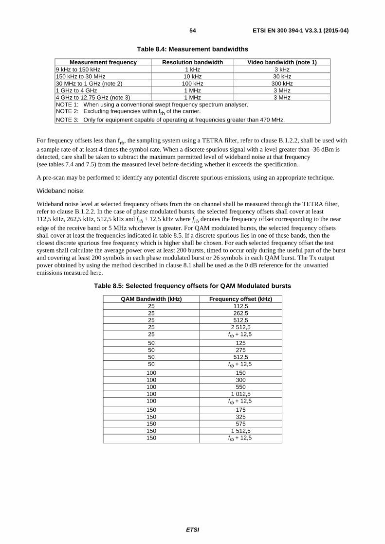
ETSI
ETSI EN 300 394-1 V3.3.1 (2015-04)54
Table 8.4: Measurement bandwidths
Measurement frequency Resolution bandwidth Video bandwidth (note 1) 9 kHz to 150 kHz 1 kHz 3 kHz 150 kHz to 30 MHz 10 kHz 30 kHz 30 MHz to 1 GHz (note 2) 100 kHz 300 kHz 1 GHz to 4 GHz 1 MHz 3 MHz 4 GHz to 12,75 GHz (note 3) 1 MHz 3 MHz NOTE 1: When using a conventional swept frequency spectrum analyser. NOTE 2: Excluding frequencies within frb of the carrier.
NOTE 3: Only for equipment capable of operating at frequencies greater than 470 MHz.
For frequency offsets less than frb, the sampling system using a TETRA filter, refer to clause B.1.2.2, shall be used with
a sample rate of at least 4 times the symbol rate. When a discrete spurious signal with a level greater than -36 dBm is detected, care shall be taken to subtract the maximum permitted level of wideband noise at that frequency (see tables 7.4 and 7.5) from the measured level before deciding whether it exceeds the specification.
A pre-scan may be performed to identify any potential discrete spurious emissions, using an appropriate technique.
Wideband noise:
Wideband noise level at selected frequency offsets from the on channel shall be measured through the TETRA filter, refer to clause B.1.2.2. In the case of phase modulated bursts, the selected frequency offsets shall cover at least 112,5 kHz, 262,5 kHz, 512,5 kHz and frb + 12,5 kHz where frb denotes the frequency offset corresponding to the near
edge of the receive band or 5 MHz whichever is greater. For QAM modulated bursts, the selected frequency offsets shall cover at least the frequencies indicated in table 8.5. If a discrete spurious lies in one of these bands, then the closest discrete spurious free frequency which is higher shall be chosen. For each selected frequency offset the test system shall calculate the average power over at least 200 bursts, timed to occur only during the useful part of the burst and covering at least 200 symbols in each phase modulated burst or 26 symbols in each QAM burst. The Tx output power obtained by using the method described in clause 8.1 shall be used as the 0 dB reference for the unwanted emissions measured here.
Table 8.5: Selected frequency offsets for QAM Modulated bursts
QAM Bandwidth (kHz) Frequency offset (kHz) 25 112,5 25 262,5 25 512,5 25 2 512,5 25 frb + 12,5
50 125 50 275 50 512,5 50 frb + 12,5
100 150 100 300 100 550 100 1 012,5 100 frb + 12,5
150 175 150 325 150 575 150 1 512,5 150 frb + 12,5
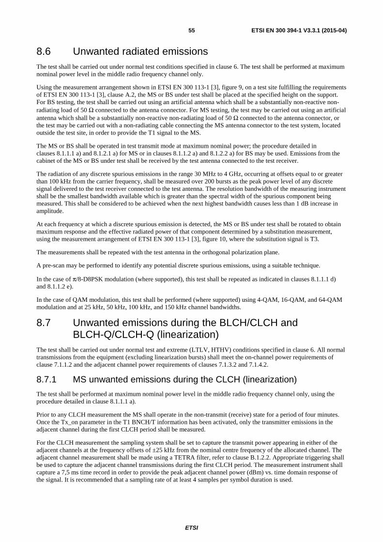
ETSI
ETSI EN 300 394-1 V3.3.1 (2015-04)55
8.6 Unwanted radiated emissions The test shall be carried out under normal test conditions specified in clause 6. The test shall be performed at maximum nominal power level in the middle radio frequency channel only.
Using the measurement arrangement shown in ETSI EN 300 113-1 [3], figure 9, on a test site fulfilling the requirements of ETSI EN 300 113-1 [3], clause A.2, the MS or BS under test shall be placed at the specified height on the support. For BS testing, the test shall be carried out using an artificial antenna which shall be a substantially non-reactive non-radiating load of 50 Ω connected to the antenna connector. For MS testing, the test may be carried out using an artificial antenna which shall be a substantially non-reactive non-radiating load of 50 Ω connected to the antenna connector, or the test may be carried out with a non-radiating cable connecting the MS antenna connector to the test system, located outside the test site, in order to provide the T1 signal to the MS.
The MS or BS shall be operated in test transmit mode at maximum nominal power; the procedure detailed in clauses 8.1.1.1 a) and 8.1.2.1 a) for MS or in clauses 8.1.1.2 a) and 8.1.2.2 a) for BS may be used. Emissions from the cabinet of the MS or BS under test shall be received by the test antenna connected to the test receiver.
The radiation of any discrete spurious emissions in the range 30 MHz to 4 GHz, occurring at offsets equal to or greater than 100 kHz from the carrier frequency, shall be measured over 200 bursts as the peak power level of any discrete signal delivered to the test receiver connected to the test antenna. The resolution bandwidth of the measuring instrument shall be the smallest bandwidth available which is greater than the spectral width of the spurious component being measured. This shall be considered to be achieved when the next highest bandwidth causes less than 1 dB increase in amplitude.
At each frequency at which a discrete spurious emission is detected, the MS or BS under test shall be rotated to obtain maximum response and the effective radiated power of that component determined by a substitution measurement, using the measurement arrangement of ETSI EN 300 113-1 [3], figure 10, where the substitution signal is T3.
The measurements shall be repeated with the test antenna in the orthogonal polarization plane.
A pre-scan may be performed to identify any potential discrete spurious emissions, using a suitable technique.
In the case of π/8-D8PSK modulation (where supported), this test shall be repeated as indicated in clauses 8.1.1.1 d) and 8.1.1.2 e).
In the case of QAM modulation, this test shall be performed (where supported) using 4-QAM, 16-QAM, and 64-QAM modulation and at 25 kHz, 50 kHz, 100 kHz, and 150 kHz channel bandwidths.
8.7 Unwanted emissions during the BLCH/CLCH and BLCH-Q/CLCH-Q (linearization)
The test shall be carried out under normal test and extreme (LTLV, HTHV) conditions specified in clause 6. All normal transmissions from the equipment (excluding linearization bursts) shall meet the on-channel power requirements of clause 7.1.1.2 and the adjacent channel power requirements of clauses 7.1.3.2 and 7.1.4.2.
8.7.1 MS unwanted emissions during the CLCH (linearization)
The test shall be performed at maximum nominal power level in the middle radio frequency channel only, using the procedure detailed in clause 8.1.1.1 a).
Prior to any CLCH measurement the MS shall operate in the non-transmit (receive) state for a period of four minutes. Once the Tx_on parameter in the T1 BNCH/T information has been activated, only the transmitter emissions in the adjacent channel during the first CLCH period shall be measured.
For the CLCH measurement the sampling system shall be set to capture the transmit power appearing in either of the adjacent channels at the frequency offsets of ±25 kHz from the nominal centre frequency of the allocated channel. The adjacent channel measurement shall be made using a TETRA filter, refer to clause B.1.2.2. Appropriate triggering shall be used to capture the adjacent channel transmissions during the first CLCH period. The measurement instrument shall capture a 7,5 ms time record in order to provide the peak adjacent channel power (dBm) vs. time domain response of the signal. It is recommended that a sampling rate of at least 4 samples per symbol duration is used.
ETSI
ETSI EN 300 394-1 V3.3.1 (2015-04)56
The measurement instrument provides a peak adjacent channel power "dBm" reading for CLCH period measured. To obtain a "dBc" reading the measured "dBm" value is then subtracted from the normal average on-channel "dBm" power level, as measured at maximum nominal power level in clause 8.1 under the appropriate test conditions.
8.7.2 BS unwanted emissions during the BLCH (linearization)
The test shall be performed at maximum nominal power level in the middle radio frequency channel only, using the procedure detailed in clause 8.1.1.2 a).
Prior to any BLCH measurement, the BS shall be operating in BS test transmit mode as defined in clause 5.2.2.3.
For the BLCH measurement the sampling system shall be set to capture the transmit power appearing in either of the adjacent channels at the frequency offsets of ±25 kHz from the nominal centre frequency of the allocated channel. The adjacent channel measurement shall be made using a TETRA filter, refer to clause B.1.2.2. The adjacent channel transmissions during a BLCH period shall be captured by timing the measurement to occur during block 2 of a Normal Downlink Burst with Normal Training Sequence 2, defined in ETSI EN 300 392-2 [1], clause 9. The measurement instrument shall capture a 6,0 ms time record in order to provide the peak adjacent channel power (dBm) vs. time domain response of the signal. It is recommended that a sampling rate of at least 4 samples per symbol duration is used.
The measurement instrument provides a peak adjacent channel power "dBm" reading for BLCH period measured. To obtain a "dBc" reading the measured "dBm" value is then subtracted from the normal average on-channel "dBm" power level, as measured at maximum nominal power level in clause 8.1 under the appropriate test conditions.
8.7.3 MS unwanted emissions during the CLCH-Q (linearization)
The test shall be performed at maximum nominal power level in the middle radio frequency channel only, using the procedure detailed in clause 8.1.2.1 a).
Prior to any CLCH-Q measurement the MS shall operate in the non-transmit (receive) state for a period of four minutes. Once the Tx_on parameter in the T1 BNCH/T information has been activated, only the transmitter emissions in the adjacent channel during the first CLCH-Q period shall be measured.
For the CLCH-Q measurement the sampling system shall be set to capture the transmit power appearing in either of the adjacent channels at the frequency offsets specified in clause 7.1.7.3 from the nominal centre frequency of the allocated channel. The adjacent channel measurement shall be made using a TETRA filter, refer to clause B.1.2.2. Appropriate triggering shall be used to capture the adjacent channel transmissions during the first CLCH period. The measurement instrument shall capture a 7,5 ms time record in order to provide the peak adjacent channel power (dBm) vs. time domain response of the signal. It is recommended that a sampling rate of at least 4 samples per symbol duration is used.
The measurement instrument provides a peak adjacent channel power "dBm" reading for CLCH-Q period measured. To obtain a "dBc" reading the measured "dBm" value is then subtracted from the normal average on-channel "dBm" power level, as measured at maximum nominal power level in clause 8.1 under the appropriate test conditions.
This test shall be performed (where supported) at 25 kHz, 50 kHz, 100 kHz, and 150 kHz channel bandwidths.
8.7.4 BS unwanted emissions during the BLCH-Q (linearization)
The test shall be performed at maximum nominal power level in the middle radio frequency channel only, using the procedure detailed in clause 8.1.2.2 a).
Prior to any BLCH-Q measurement, the BS shall be operating in BS test transmit mode as defined in clause 5.2.2.3.
For the BLCH-Q measurement the sampling system shall be set to capture the transmit power appearing in either of the adjacent channels at the frequency offsets specified in clause 7.1.7.3 from the nominal centre frequency of the allocated channel. The adjacent channel measurement shall be made using a TETRA filter, refer to clause B.1.2.2. The adjacent channel transmissions during a BLCH-Q period shall be captured by timing the measurement to occur during the linearization portion of the linearization downlink burst (LDB), defined in ETSI EN 300 392-2 [1], clause 9. The measurement instrument shall capture the samples over the middle 20 symbols of linearization in order to provide the peak adjacent channel power (dBm) vs. time domain response of the signal. It is recommended that a sampling rate of at least 4 samples per symbol duration is used.
The measurement instrument provides a peak adjacent channel power "dBm" reading for BLCH-Q period measured. To obtain a "dBc" reading the measured "dBm" value is then subtracted from the normal average on-channel "dBm" power level, as measured at maximum nominal power level in clause 8.1 under the appropriate test conditions.
ETSI
ETSI EN 300 394-1 V3.3.1 (2015-04)57
This test shall be performed (where supported) at 25 kHz, 50 kHz, 100 kHz, and 150 kHz channel bandwidths.
8.8 Transmitter intermodulation attenuation The test shall be carried out under normal test conditions specified in clause 6. Referring to the test configuration presented in clause 5.1, the following equipment shall be employed:
• A spectrum analyser with 30 kHz measurement bandwidth as a power detecting device in frequency domain (clause B.1.3) and an unmodulated signal generator as an interfering signal source (test signal T3, clause 5.3.4). In addition, a directional coupler and RF attenuators shall be used to complete the measurement arrangement.
• Using the procedure detailed in clauses 8.1.1.1 a) and 8.1.2.1 a) for MS and in clauses 8.1.1.2 a) and 8.1.2.2 a) for BS, the equipment under test shall be set to test transmit mode and transmit at its maximum nominal power level on the middle radio frequency channel. The interfering (unmodulated) signal generator shall be set to deliver the desired output power level detailed below, at a frequency of 500 kHz above the transmitter under test frequency. The frequency of signal T3 shall if necessary be adjusted in steps of 25 kHz such that the intermodulation components to be measured do not coincide with other spurious components. The spectrum analyser shall be used to measure the power of any intermodulation component occurring at offsets equal to or less than 10 MHz from the carrier frequency. The test shall be repeated with the T3 signal generator frequency set to 5 MHz above, 500 kHz below and 5 MHz below the frequency of the transmitter under test.
The transmitter shall be set to produce 4-QAM modulation. This test shall be performed (where supported) at 25 kHz, 50 kHz, 100 kHz, and 150 kHz channel bandwidths.
8.8.1 MS Transmitter intermodulation attenuation
The signal generator level shall be set to deliver at the antenna connector of the transmitter under test an interfering signal (T3) at a power level 50 dB below the transmitter transmit level.
8.8.2 BS Transmitter intermodulation attenuation
The signal generator level shall be set to deliver at the antenna connector of the transmitter under test an interfering signal (T3) at a power level 30 dB below the transmitter transmit level.
8.8.3 Intra BS transmitter intermodulation attenuation
In the case of intra BS intermodulation, the individual transmitters shall be set to their nominal power levels and test signal T3 shall be switched off.
9 Methods of measurement for receiver parameters
9.1 General Unless otherwise stated the equipment under test shall be operated in either the non-transmit state or the non-active transmit state.
9.2 Nominal error rates for phase modulation The test shall be carried out under normal test conditions specified in clause 6. A test configuration as presented in clause 5.1 should be applied. The equipment under test shall be connected to the test system via its antenna connector.
NOTE: There are no nominal error rates for QAM.
9.2.1 MS nominal error rate
a) The MS is set up to receive a T1 signal with channel type 1 burst in the middle radio frequency channel of the MS receive band. The propagation simulator function is set to TU50, defined in ETSI EN 300 392-2 [1], clause 6.8.3. The test system shall transmit test signal T1 such that the power level at the antenna connector of the MS is -85 dBm.

ETSI
ETSI EN 300 394-1 V3.3.1 (2015-04)58
b) At the test connector the error events in the received data shall be captured and the appropriate BER shall be calculated (refer to clause A.2).
c) Step b) shall be repeated for all test cases (where supported) defined in clause 7.2.2.
9.2.2 BS nominal error rate
a) The BS shall operate in its normal mode and shall transmit on timeslot 1 of frame 18 a synchronization burst containing BNCH/T information. The BNCH/T is used to indicate which channel type the BS expects the test system to send on timeslot 1 of the corresponding uplink channel in frames 1 to 18. A BS in continuous mode shall in time slots 1 to 4 of frames 1 to 17 and time slots 2 to 4 of frame 18, send a channel type 1 signal. For a discontinuous BS a channel type 1 signal shall be sent on timeslot 1 of frames 1 to 17 only.
b) The BS is set up to receive a T1 signal with channel type 7 burst in the middle radio frequency channel of the BS receive band. The propagation simulator function is set to TU50, defined in ETSI EN 300 392-2 [1], clause 6.8.3. The test system shall transmit test signal T1 such that the power level at the antenna connector of the BS is -85 dBm.
c) At the test connector the error events in the received data shall be captured and the appropriate BER shall be calculated (refer to clause A.2).
d) Step b) shall be repeated for all test cases (where supported) defined in clause 7.2.2.
9.3 Reference sensitivity performance The test shall be carried out under normal and where applicable extreme (LTLV, HTHV) test conditions specified in clause 6. A test configuration as presented in clause 5.1 should be applied. The equipment shall be connected to the test system via its antenna connector.
9.3.1 MS reference sensitivity performance for phase modulation
a) Using test signal T1 the MS is set up to receive one of the logical channels defined in clause 7.2.3.2. The propagation simulator function shall be set according to clause 7.2.3.2. The test system shall provide the test signal T1, under normal test conditions, at a power level of -103 dBm.
b) At the test connector the error events in the received data shall be captured and the appropriate error rate shall be calculated.
c) Step b) shall be repeated for all test cases defined in clause 7.2.3.2.
In order to reduce test time, only the MS receiver sensitivity test using channel type 2, shall be conducted under both normal and extreme test conditions. Under extreme test conditions the test system shall provide the test signal T1, at a power level of -97 dBm. Channel type 2 receiver sensitivity measurements shall also be repeated in the highest, middle and lowest channels of the receive band. In all other MS test cases the receiver sensitivity test shall only be performed in the middle channel of the receive band under normal conditions.
9.3.2 BS reference sensitivity performance for phase modulation
a) Using the test set-up outlined in clause 9.2.2 the BS shall be set up to receive one of the logical channels defined in clause 7.2.3.2. The test system shall provide the test signal T1 at a power level of -106 dBm.
- In order to reduce test time, only the BS receiver sensitivity test using channel type 8, shall be conducted under both normal and extreme test conditions. Under extreme test conditions the test system shall provide the test signal, at a power level of -100 dBm. Channel type 8 receiver sensitivity measurements shall also be repeated in the highest, middle and lowest channels of the receive band. In all other BS test cases the receiver sensitivity test shall only be performed in the middle channel of the receive band under normal conditions.
b) At the test connector the error events in the received data shall be captured and the appropriate error rate shall be calculated.
c) Step b) shall be repeated for all test cases defined in clause 7.2.3.2.
ETSI
ETSI EN 300 394-1 V3.3.1 (2015-04)59
9.3.3 MS reference sensitivity performance for QAM
a) Using the test set-up described in clause 5.2.1.3 for QAM MS test receive mode, the MS is set up to receive one of the logical channels defined in clause 7.2.3.3. The propagation simulator function shall be set according to clause 7.2.3.3. The test system shall provide the test signal T4 at a power level based on the modulation type and channel bandwidth from clause 7.2.3.3.
b) At the test connector the error events in the received data shall be captured and the appropriate error rate shall be calculated.
c) Step b) shall be repeated (where supported) for all test cases defined in clause 7.2.3.3.
9.3.4 BS reference sensitivity performance for QAM
a) Using the test set-up described in clause 5.2.1.4 for QAM BS test receive mode, the BS shall be set up to receive one of the logical channels defined in clause 7.2.3.3. The propagation simulator function shall be set according to clause 7.2.3.3. The test system shall provide the test signal T4 at a power level based on the modulation type and channel bandwidth from clause 7.2.3.3.
b) At the test connector the error events in the received data shall be captured and the appropriate error rate shall be calculated.
c) Step b) shall be repeated (where supported) for all test cases defined in clause 7.2.3.3.
9.3.5 PUEM performance
The PUEM performance of the receiver under test at reference sensitivity shall be measured, the test cases and conditions are detailed in the PUEM test table in clause A.2. The receiver under test shall provide along with the recovered data a message error flag at the test connector. The test system shall record those instances when a message error occurred, but the message error flag was not set. Following the completion of PUEM testing on the equipment, the test system shall generate a PUEM figure for each test case.
9.4 Reference interference performance The tests shall be carried out under normal and in the case of adjacent channel interference, also extreme (LTLV, HTHV) test conditions specified in clause 6. A test configuration as presented in clause 5.1 should be applied. The equipment shall be connected to the test system.
9.4.1 MS reference interference performance for phase modulation
a) The MS is set up to receive one of the logical channels defined for co-channel interference in clause 7.2.4.2 on a radio frequency channel in the middle of the MS receive band. The propagation simulator functions (for wanted and unwanted signals) shall be set according to clause 7.2.4.2. The test system shall provide the test signal T1 (wanted signal at the nominal frequency of the MS receiver) with a power level of -85 dBm at the antenna connector of the MS.
b) The interfering signal source shall provide the phase modulated test signal T2 (unwanted signal) at the nominal frequency of the MS receiver and with a power level of -104 dBm at the antenna connector of the MS.
c) At the test connector the error events in the received data shall be captured and the appropriate error rate calculated.
d) Step c) shall be repeated for all co-channel interference test cases defined in clause 7.2.4.2.
e) The test system shall provide the wanted test signal T1 with a power level of -100 dBm (normal test conditions) or -94 dBm (extreme test conditions). The interfering signal source shall be set to provide the unwanted phase modulated test signal T2 at the frequency offsets of ±25 kHz from the nominal frequency of the MS receiver and with a power level of -60 dBm (normal) or -64 dBm (extreme).
f) Step c) shall be repeated for all adjacent channel interference test cases defined in clause 7.2.4.2.
ETSI
ETSI EN 300 394-1 V3.3.1 (2015-04)60
9.4.2 BS reference interference performance for phase modulation
a) Using the test set-up outlined in clause 9.2.2 the BS shall be set up to receive one of the logical channels defined for co-channel interference in clause 7.2.4.2. on a radio frequency channel in the middle of the BS receive band. The propagation simulator functions (for wanted and unwanted signals) shall be set according to clause 7.2.4.2. The test system shall provide the test signal T1 (wanted signal at the nominal frequency of the BS receiver) with a power level of -85 dBm at the antenna connector of the BS.
b) The interfering signal source shall provide the phase modulated test signal T2(unwanted signal) at the nominal frequency of the BS receiver and with a power level of -104 dBm at the antenna connector of the BS.
c) At the test connector the error events in the received data shall be captured and the appropriate error rate calculated.
d) Step c) shall be repeated for all co-channel interference test cases defined in clause 7.2.4.2.
e) The test system shall provide the wanted test signal at a power level of -103 dBm (normal test conditions) or -97 dBm (extreme test conditions). The interfering signal source shall be set to provide the unwanted phase modulated test signal T2 at the frequency offsets of ±25 kHz from the nominal frequency of the BS receiver and with a power level of -58 dBm (normal) or -62 dBm (extreme) for frequencies less than 700 MHz, and -63 dBm (normal) or -67 dBm (extreme) for frequencies above 700 MHz.
f) Step c) shall be repeated for all adjacent channel interference test cases defined in clause 7.2.4.2.
9.4.3 MS reference interference performance for QAM
a) Using the test set-up described in clause 5.2.1.3 for QAM MS test receive mode, the MS shall be set up to receive one of the logical channels defined for co-channel interference in clause 7.2.4.3 on a radio frequency channel in the middle of the MS receive band. The propagation simulator functions (for wanted and unwanted signals) shall be set according to clause 7.2.4.3. The test system shall provide the test signal T4 (wanted signal at the nominal frequency of the MS receiver) with the power level indicated in clause 7.2.4.3 at the antenna connector of the MS.
b) The interfering signal source shall provide the QAM modulated test signal T2 (unwanted signal) at the nominal frequency of the MS receiver and with the power level indicated in clause 7.2.4.3 at the antenna connector of the MS. The bandwidth and modulation shall be the same as the test signal T4.
c) At the test connector the error events in the received data shall be captured and the appropriate error rate calculated.
d) Step c) shall be repeated (where supported) for all co-channel interference test cases defined in clause 7.2.4.3.
e) The test system shall provide the wanted test signal T4 with the power level indicated in clause 7.2.4.3. The interfering signal source shall be set to provide the phase modulated test signal T2 (unwanted signal) at the frequency offset and power level indicated in clause 7.2.4.3.
f) Step c) shall be repeated (where supported) for all adjacent channel interference test cases defined in clause 7.2.4.3.
9.4.4 BS reference interference performance for QAM
a) Using the test set-up described in clause 5.2.1.4 for QAM BS test receive mode, the BS shall be set up to receive one of the logical channels defined for co-channel interference in clause 7.2.4.3 on a radio frequency channel in the middle of the BS receive band. The propagation simulator functions (for wanted and unwanted signals) shall be set according to clause 7.2.4.3. The test system shall provide the test signal T4 (wanted signal at the nominal frequency of the BS receiver) with the power level indicated in clause 7.2.4.3 at the antenna connector of the BS.
b) The interfering signal source shall provide the QAM modulated test signal T2 (unwanted signal) at the nominal frequency of the BS receiver and with the power level indicated in clause 7.2.4.3 at the antenna connector of the BS. The bandwidth and modulation shall be the same as the test signal T4.
c) At the test connector the error events in the received data shall be captured and the appropriate error rate calculated.
ETSI
ETSI EN 300 394-1 V3.3.1 (2015-04)61
d) Step c) shall be repeated (where supported) for all co-channel interference test cases defined in clause 7.2.4.3.
e) The test system shall provide the wanted test signal at the power level indicated in clause 7.2.4.3. The interfering signal source shall be set to provide the unwanted phase modulated test signal T2 (unwanted signal) at the frequency offsets and power level indicated in clause 7.2.4.3.
f) Step c) shall be repeated (where supported) for all adjacent channel interference test cases defined in clause 7.2.4.3.
9.5 Blocking characteristics The test shall be carried out under normal test conditions specified in clause 6. The test configuration presented in clause 5.1 is applied. The error rate indication scheme used in clauses 9.3 and 9.4 may be employed. All propagation simulator functions are set to "static". The equipment shall be connected to the test system.
9.5.1 MS blocking for phase modulation
a) The MS is set up to receive a T1 channel type 1 signal (i.e. TCH/7,2) on a radio frequency channel in the middle of the MS receive band. The test system shall provide the wanted test signal T1 at a power level of -109 dBm at the antenna connector of the MS.
b) The interfering signal source shall provide the test signal T3 (unmodulated unwanted signal) at frequency offsets of approximately ±1 MHz, ±2 MHz, ±5 MHz and ±10 MHz from the nominal frequency of the MS receiver at a power level of -25 dBm. The actual values of the offset frequencies shall be adjusted in steps of 25 kHz such that they do not coincide with the frequencies of spurious response to be tested in clause 9.6.
c) For each of the offset frequencies chosen in step b) the bit error rate shall be indicated.
9.5.2 BS blocking for phase modulation
a) Using the test set-up outlined in clause 9.2.2 the BS shall be set up to receive a T1 channel type 7, on a radio frequency channel in the middle of the BS receive band. The test system shall provide the wanted test signal T1 at a power level of -112 dBm at the antenna connector of the BS.
b) The interfering signal source shall provide the test signal T3 (unmodulated unwanted signal) at frequency offsets of ±1 MHz, ±2 MHz, ±5 MHz and ±10 MHz from the nominal frequency of the BS receiver at a power level of -25 dBm. The actual values of the offset frequencies shall be adjusted in steps of 25 kHz such that they do not coincide with the frequencies of spurious response to be tested in clause 9.6.
c) For each of the offset frequencies chosen in step b) the bit error rate shall be indicated.
9.5.3 MS blocking for QAM
a) Using the test set-up described in clause 5.2.1.3 for QAM MS test receive mode, the MS shall be set up to receive a T4 channel type 27 signal (i.e. SCH-Q/D) on a radio frequency channel in the middle of the MS receive band. The test system shall provide the wanted test signal T4 at the power level indicated in clause 7.2.5.3 at the antenna connector of the MS.
b) The interfering signal source shall provide the test signal T3 (unmodulated unwanted signal) at frequency offsets and power levels from clause 7.2.5.3. The power level of the interfering signal is related to the frequency offset of the interferer and is given in tables 7.28, 7.29, 7.30, and 7.31. The actual values of the offset frequencies shall be adjusted in steps of 25 kHz such that they do not coincide with the frequencies of spurious response to be tested in clause 9.6.
c) For each of the offset frequencies chosen in step b) the bit error rate shall be indicated.
d) This test should be repeated (where supported) for each of the test cases in clause 7.2.5.3 at each of 4-QAM, 16-QAM and 64-QAM (where supported).

ETSI
ETSI EN 300 394-1 V3.3.1 (2015-04)62
9.5.4 BS blocking for QAM
a) Using the test set-up described in clause 5.2.1.4 for QAM BS test receive mode, the BS shall be set up to receive a T4 channel type 26 signal (i.e. SCH-Q/U), on a radio frequency channel in the middle of the BS receive band. The test system shall provide the test signal T4 (wanted signal at the nominal frequency of the BS receiver) with the power level indicated in clause 7.2.5.3 at the antenna connector of the BS.
b) The interfering signal source shall provide the test signal T3 (unmodulated unwanted signal) at frequency offsets and power levels from clause 7.2.5.3. The power level of the interfering signal is related to the frequency offset of the interferer and is given in tables 7.28 to 7.31. The actual values of the offset frequencies shall be adjusted in steps of 25 kHz such that they do not coincide with the frequencies of spurious response to be tested in clause 9.6.
c) For each of the offset frequencies chosen in step b) the bit error rate shall be indicated.
d) This test should be repeated (where supported) for each of the test cases in clause 7.2.5.3.
9.6 Spurious response rejection The tests shall be carried out under the normal test conditions specified in clause 6. The tests shall be performed in the middle radio frequency channel only.
9.6.1 Phase Modulation
a) The same test configuration and conditions as in clause 9.5 with exceptions are applied. The frequency of the interfering signal is set to the frequencies as defined in clause A.1, and the power level of the interfering signal is set to the level specified in ETSI EN 300 392-2 [1], table 6.21: Blocking levels of the receiver. For each interfering frequency the error rate shall be measured. An interfering frequency where the blocking bit error rate limits in clause A.2 is not fulfilled is defined as a spurious response frequency.
b) For each spurious response frequency the error rate shall be measured with a power level of the interfering signal of -45 dBm.
c) For each of the spurious response frequencies found in step a) the frequency and bit error rate shall be indicated.
9.6.2 QAM
a) The same test configuration and conditions as in clause 9.5 with exceptions are applied. The frequency of the interfering signal is set to the frequencies as defined in clause A.1, and the power level of the interfering signal is set to the level specified in ETSI EN 300 392-2 [1], tables 6.22 to 6.25. For each interfering frequency the error rate shall be measured. An interfering frequency where the blocking bit error rate limits in clause A.2 is not fulfilled is defined as a spurious response frequency.
b) For each spurious response frequency the error rate shall be measured with a power level of the interfering signal of -45 dBm.
c) For each of the spurious response frequencies found in step a) the frequency and bit error rate shall be indicated.
d) This test should be repeated (where supported) for each of the test cases in clause 7.2.6.3.
9.7 Intermodulation response rejection The test shall be carried out under normal test conditions specified in clause 6. The test configuration presented in clause 5.1 is applied. The error rate indication scheme used in clauses 9.2 to 9.4 may be employed. All propagation simulator functions are set to "static". The equipment under test shall be connected to the test system.
9.7.1 MS intermodulation response rejection for phase modulation
a) The MS is set up to receive a T1 channel type 1 signal (i.e. TCH/7,2) on a radio frequency channel f0 in the
middle of the MS receive band. The test system shall provide the wanted test signal T1 at a power level of -109 dBm at the antenna connector of the MS.

ETSI
ETSI EN 300 394-1 V3.3.1 (2015-04)63
b) The unmodulated interfering signal source shall provide the test signal T3 (unmodulated unwanted signal) at frequency (f1 = f0 - 200 kHz) and with a power level of -47 dBm. The modulated interfering signal source shall provide the phase modulated test signal T2 (modulated unwanted signal) at frequency (f2 = f0 - 400 kHz) and with a power level of -47 dBm. Both unwanted power levels refer to the antenna connector of the MS.
c) The error events in the received data shall be captured and the appropriate error rate shall be calculated.
d) Step c) shall be repeated with the unwanted signal frequencies set to (f1 = f0 + 200 kHz) and (f2 = f0 + 400 kHz).
9.7.2 BS intermodulation response rejection for phase modulation
a) Using the test set-up outlined in clause 9.2.2 the BS shall be set up to receive a T1 channel type 7, on a radio frequency channel f0 in the middle of the BS receive band. The test system shall provide the wanted test signal
T1 at a power level of -112 dBm at the antenna connector of the BS.
b) The unmodulated interfering signal source shall provide the test signal T3 (unmodulated unwanted signal) at frequency (f1 = f0 - 200 kHz) and with a power level of -47 dBm. The modulated interfering signal source shall provide the phase modulated test signal T2 (modulated unwanted signal) at frequency (f2 = f0 - 400 kHz) and with a power level of -47 dBm. Both unwanted power levels refer to the antenna connector of the BS.
c) The error events in the received data shall be captured and the appropriate error rate shall be calculated.
d) Step c) shall be repeated with the unwanted signal frequencies set to (f1 = f0 + 200 kHz) and (f2 = f0 + 400 kHz).
9.7.3 MS intermodulation response rejection for QAM
a) Using the test set-up described in clause 5.2.1.3 for QAM MS test receive mode, the MS shall be set up to receive a T4 channel type 27 signal (i.e. SCH-Q/D) on a radio frequency channel f0 in the middle of the MS
receive band. The test system shall provide the wanted test signal T4 at the power level indicated in clause 7.2.7.2 at the antenna connector of the MS. The modulation should be set to 4-QAM and the bandwidth should be set to 25 kHz.
b) The unmodulated interfering signal source shall provide the test signal T3 (unmodulated unwanted signal) at frequency (f1 = f0 - fx) and with a power level of -47 dBm. The modulated interfering signal source shall provide the phase modulated test signal T2 (modulated unwanted signal) at frequency (f2 = f0 - 2fx) and with a power level of -47 dBm. The value fx comes from table 7.33. Both unwanted power levels refer to the antenna connector of the MS.
c) The error events in the received data shall be captured and the appropriate error rate shall be calculated.
d) Step c) shall be repeated with the unwanted signal frequencies set to (f1 = f0 + f x) and (f2 = f0 + 2f x).
e) Steps b), c), and d) should be repeated (where supported) using 50 kHz, 100 kHz, and 150 kHz channel bandwidths for the wanted signal T4.
9.7.4 BS intermodulation response rejection for QAM
a) Using the test set-up described in clause 5.2.1.4 for QAM BS test receive mode, the BS shall be set up to receive a T4 channel type 26 signal (i.e. SCH-Q/U), on a radio frequency channel f0 in the middle of the BS receive band. The test system shall provide the wanted test signal T4 at a power level indicated in clause 7.2.7.2 at the antenna connector of the BS. The modulation should be set to 4-QAM and the bandwidth should be set to 25 kHz.
b) The unmodulated interfering signal source shall provide the test signal T3 (unmodulated unwanted signal) at frequency (f1 = f0 – fx) and with a power level of -47 dBm. The modulated interfering signal source shall provide the phase modulated test signal T2 (modulated unwanted signal) at frequency (f2 = f0 – 2fx) and with a power level of -47 dBm. Both unwanted power levels refer to the antenna connector of the BS. The value fx comes from table 7.33.
ETSI
ETSI EN 300 394-1 V3.3.1 (2015-04)64
c) The error events in the received data shall be captured and the appropriate error rate shall be calculated.
d) Step c) shall be repeated with the unwanted signal frequencies set to (f1 = f0 + f x) and (f2 = f0 + 2f x).
e) Steps b, c, and d should be repeated (where supported) using 50 kHz, 100 kHz, and 150 kHz channel bandwidths for the wanted signal T4.
9.8 Unwanted emissions The test shall be carried out under normal test conditions specified in clause 6.
The equipment shall be connected to the test system via its antenna connector. The equipment shall be in receive mode in the non-transmit state. For equipment only capable of operating at frequencies below 470 MHz, the test system shall measure the peak power emitted by the equipment in the frequency range 9 kHz to 4 GHz. For equipment capable of operating at frequencies above 470 MHz, the test system shall measure the peak power emitted by the equipment in the frequency range 9 kHz to 12,75 GHz. Discrete spurious emissions shall be measured as a peak power level of any discrete signal delivered to a spectrum analyser suitably connected to the antenna port of the equipment (defined in clause B.1.3). The resolution bandwidth of the spectrum analyser shall be 100 kHz for frequencies up to 1 GHz and 1 MHz for frequencies above 1 GHz. When measuring in the frequency range below 3 MHz the measurement bandwidth shall be reduced according to specifications of the spectrum analyser. The test shall be performed on the middle radio frequency channel only of the equipment's receive band.
9.9 Unwanted radiated emissions The test shall be carried out under normal test conditions specified in clause 6. The test shall be performed with the equipment in receive mode in the non-transmit state in the middle radio frequency channel only.
Using the measurement arrangement shown in ETSI EN 300 113-1 [3], figure 9, on a test site fulfilling the requirements of ETSI EN 300 113-1 [3], clause A.2, the MS or BS under test shall be placed at the specified height on the support. For BS testing, the test shall be carried out using an artificial antenna which shall be a substantially non-reactive non-radiating load of 50 Ω connected to the antenna connector. For MS testing, the test may be carried out using an artificial antenna which shall be a substantially non-reactive non-radiating load of 50 Ω connected to the antenna connector, or the test may be carried out with a non-radiating cable connecting the MS antenna connector to the test system, located outside the test site, in order to provide the T1 signal to the MS.
The MS or BS shall be operated in test receive mode in the non-transmit state. Emissions from the cabinet of the MS or BS under test shall be received by the test antenna connected to the test receiver.
The radiation of any discrete spurious emissions in the range 30 MHz to 4 GHz, occurring at offsets equal to or greater than 100 kHz from the carrier frequency, shall be measured over 200 bursts as the peak power level of any discrete signal delivered to the test receiver connected to the test antenna. The resolution bandwidth of the measuring instrument shall be the smallest bandwidth available which is greater than the spectral width of the spurious component being measured. This shall be considered to be achieved when the next highest bandwidth causes less than 1 dB increase in amplitude.
At each frequency at which a discrete spurious emission is detected, the MS or BS under test shall be rotated to obtain maximum response and the effective radiated power of that component determined by a substitution measurement, using the measurement arrangement of ETSI EN 300 113-1 [3], figure 10, where the substitution signal is T3.
The measurements shall be repeated with the test antenna in the orthogonal polarization plane.
A pre-scan may be performed to identify any potential discrete spurious emissions, using a suitable technique.
10 Methods of measurement for transmitter/receiver parameters
10.1 Modulation accuracy The test shall be carried out at maximum nominal power only under normal test conditions specified in clause 6. The test configuration presented in clause 5.1 is applied. The sampling system in clause B.1.2 shall be employed.
ETSI
ETSI EN 300 394-1 V3.3.1 (2015-04)65
10.1.1 MS modulation accuracy for phase modulation
This measurement shall be performed on a Normal Uplink Burst with Normal Training Sequence 1 (to exclude any BLCH transmissions), defined in ETSI EN 300 392-2 [1], clause 9. The MS shall be connected to the test system. The test system shall transmit test signal T1. Test signal T1 BNCH/T parameters and level as detailed in test case 1 of clause 8.1.1.1 a) shall be used. All T1 levels are referenced to the antenna connector of the MS.
The MS shall be set to test receive mode for a period of at least 5 s in which it will decode BSCH and BNCH/T information and measure T1 signal strength. The MS shall then be set to test transmit mode. The modulation accuracy shall be tested by measuring the vector error magnitude as specified in clause 10.1.3.
This test shall be repeated with a π/8-D8PSK modulated T1 signal type (where supported) as detailed in clause 8.1.1.1 d).
10.1.2 BS modulation accuracy for phase modulation
This measurement shall be performed on a Normal Downlink Bursts with Normal Training Sequence 1 (to exclude any BLCH transmissions), defined in ETSI EN 300 392-2 [1], clause 9. The BS shall be connected to the test system. The test procedure detailed in clause 8.1.1.2 a) shall be used. The modulation accuracy shall be tested by measuring the vector error magnitude as specified in clause 10.1.3.
This test shall be repeated with a π/8-D8PSK modulated T1 signal type (where supported) as detailed in clause 8.1.1.2 e).
10.1.3 Vector error magnitude at symbol time for phase modulation
a) The sampling system shall capture a representation of the transmit burst's vector error at sampling times tk
(symbol by symbol) where tk is the symbol time corresponding to the kth symbol. For each symbol the sampling system shall compute the vector error Z'(k) - S(k) defined in ETSI EN 300 392-2 [1], clause 6.6.1.2, where Z'(k) is the normalized modulation symbol transmitted by the MS and S(k) is the modulation symbol which would be transmitted by an ideal MS. The sampling system shall calculate the RMS vector error RMSVE for all symbols of the burst as defined in ETSI EN 300 392-2 [1], clause 6.6.1.2. The sampling system shall also calculate the peak vector error magnitude |Z'(k)-S(k)| and the residual carrier magnitude C0
as defined in ETSI EN 300 392-2 [1], clause 6.6.1.2 for each symbol of the burst and shall calculate the mean residual carrier magnitude <C0> averaged over all values C0 of the burst.
b) The procedure described in step a) shall be repeated for 200 bursts.
c) The procedures described in steps a) and b) shall be performed on the lowest, highest and middle radio frequency channel in the transmit band.
10.1.4 MS modulation accuracy for QAM
The MS shall be connected to the test system. The test system shall transmit test signal T4 as detailed in clause 8.1.2.1 a). All T4 levels are referenced to the antenna connector of the MS.
The MS shall be set to test receive mode for a period of at least 5 s in which it will decode BSCH and BNCH/T information and measure T4 signal strength. The MS shall then be set to test transmit mode. The modulation accuracy shall be tested by measuring the vector error magnitude as specified in clause 10.1.6.
This test shall be performed (where supported) using 4-QAM, 16-QAM, and 64-QAM modulation and at 25 kHz, 50 kHz, 100 kHz, and 150 kHz channel bandwidths.
10.1.5 BS modulation accuracy for QAM
The BS shall be connected to the test system and shall be set to test transmit mode using a QAM normal downlink burst type. The BS shall transmit at the BS maximum nominal output power level. The modulation accuracy shall be tested by measuring the vector error magnitude as specified in clause 10.1.6.
This test shall be performed (where supported) using 4-QAM, 16-QAM, and 64-QAM modulation and at 25 kHz, 50 kHz, 100 kHz, and 150 kHz channel bandwidths.
ETSI
ETSI EN 300 394-1 V3.3.1 (2015-04)66
10.1.6 Vector error magnitude at symbol time for QAM
a) The sampling system shall capture a representation of the transmit burst's vector error at sampling times tk
(symbol by symbol) where tk is the symbol time corresponding to the kth symbol of the associated sub-carrier. For each symbol the sampling system shall compute the vector error Z'm(k) - Sm(k) defined in ETSI
EN 300 392-2 [1], clause 6.7.1.2, where Z'm(k) is the normalized modulation symbol transmitted by the MS for
an individual sub-carrier and Sm(k) is the modulation symbol which would be transmitted by an ideal MS for
an individual sub-carrier. The sampling system shall calculate the RMS vector error RMSVE for all symbols of the burst as defined in ETSI EN 300 392-2 [1], clause 6.7.1.2.
b) The procedure described in step a) shall be repeated for 200 bursts.
c) The procedures described in steps a) and b) shall be performed on the lowest, highest and middle radio frequency channel in the transmit band.
10.2 Carrier frequency accuracy The test set-up shall be according to clause 10.1.
10.2.1 MS carrier frequency accuracy for phase modulation
The sampling system shall be synchronized to the internal timing reference of the test system. The MS shall adjust its frequency by means of BSCH signals received from the test system. The MS shall be connected to the test system and the test system shall transmit test signal T1. Test signal T1 level and BNCH/T parameters as detailed in test case 1 of clause 8.1.1.1 a) shall be used. All T1 levels are referenced to the antenna connector of the MS.
The MS shall be set to test receive mode for a period of at least 5 s in which it will decode BSCH and BNCH/T information and measure T1 signal strength. The MS shall then be set to test transmit mode and the input level applied to the MS shall be the static reference sensitivity level.
a) The sampling system shall capture a representation of the MS transmit burst's modulation symbol Z(k) at sampling times tk (symbol by symbol) where tk is the symbol time corresponding to the kth symbol. For each
symbol the sampling system shall measure the phase rotation θ which is caused by the frequency difference between the MS and the sampling system, as defined in ETSI EN 300 392-2 [1], clause 6. The sampling system shall calculate the frequency error df for the burst as follows:
df = 1/(2π T SNmax) θ(k)
where df is expressed in Hz, T is the symbol duration in seconds, θ(k) is expressed in radians, and SNmax is the number of symbols in a burst.
b) The procedure described in step a) shall be repeated for 200 bursts.
c) The procedures described in steps a) and b) shall be performed on the lowest, highest and middle radio frequency channel in the MS transmit band.
d) This test shall be repeated with a π/8-D8PSK modulated T1 signal type (where supported) as detailed in clause 8.1.1.1 d).
k
SN
=∑
1
max
ETSI
ETSI EN 300 394-1 V3.3.1 (2015-04)67
10.2.2 BS carrier frequency accuracy for phase modulation
The BS shall be connected to the test system. The test procedure detailed in clause 8.1.1.2 a) shall be used. The carrier frequency accuracy shall be tested as follows:
a) The sampling system shall capture a representation of the BS transmit burst's modulation symbol Z(k) at sampling times tk (symbol by symbol) where tk is the symbol time corresponding to the kth symbol. For each
symbol the sampling system shall measure the phase rotation θ which is caused by the frequency difference between the BS and the sampling system, as defined in ETSI EN 300 392-2 [1], clause 6. The sampling system shall calculate the frequency error df for the burst as follows:
df = 1/(2π T SNmax) θ(k)
where df is expressed in Hz, T is the symbol duration in seconds, θ(k) is expressed in radians, and SNmax is the number of symbols in a burst.
b) The procedure described in step a) shall be repeated for 200 bursts.
c) If applicable the procedures described in steps a) and b) shall be performed on the lowest, highest and middle radio frequency channel in the BS transmit band.
d) This test shall be repeated with a π/8-D8PSK modulated T1 signal type (where supported) as detailed in clause 8.1.1.2 e).
10.2.3 MS carrier frequency accuracy for QAM
The MS shall be connected to the test system. The test system shall transmit test signal T4 as detailed in clause 8.1.2.1 a). All T4 levels are referenced to the antenna connector of the MS.
The MS shall be set to test receive mode for a period of at least 5 s in which it will decode BSCH and BNCH/T information and measure T4 signal strength. The MS shall then be set to test transmit mode.
a) The sampling system shall capture a representation of the transmit burst's vector error at sampling times tk
(symbol by symbol) where tk is the symbol time corresponding to the kth symbol of the associated sub-carrier.
For each symbol the sampling system shall measure the phase rotation θ which is caused by the frequency difference between the MS and the sampling system, as defined in ETSI EN 300 392-2 [1], clause 6.7.1.2. The sampling system shall calculate the frequency error df for the burst as follows:
df = 1/(2π T SNmax) θ(k)
where df is expressed in Hz, T is the symbol duration in seconds, θ(k) is expressed in radians, and SNmax is the
number of symbols in a burst.
b) The procedure described in step a) shall be repeated for 200 bursts.
c) The procedures described in steps a) and b) shall be performed on the lowest, highest and middle radio frequency channel in the MS transmit band.
d) This test shall be performed (where supported) using 4-QAM, 16-QAM, and 64-QAM modulation and at 25 kHz, 50 kHz, 100 kHz, and 150 kHz channel bandwidths.
k
SN
=∑
1
max
k
SN
=∑
1
max
ETSI
ETSI EN 300 394-1 V3.3.1 (2015-04)68
10.2.4 BS carrier frequency accuracy for QAM
The BS shall be connected to the test system. The test procedure detailed in clause 8.1.2.2 a) shall be used. The carrier frequency accuracy shall be tested as follows:
a) The sampling system shall capture a representation of the BS transmit burst's modulation symbol Z(k) at sampling times tk (symbol by symbol) where tk is the symbol time corresponding to the kth symbol of the
associated sub-carrier. For each symbol the sampling system shall measure the phase rotation θ which is caused by the frequency difference between the BS and the sampling system, as defined in ETSI EN 300 392-2 [1], clause 6.7.1.2. The sampling system shall calculate the frequency error df for the burst as follows:
df = 1/(2π T SNmax) θ(k)
where df is expressed in Hz, T is the symbol duration in seconds, θ(k) is expressed in radians, and SNmax is the number of symbols in a burst.
b) The procedure described in step a) shall be repeated for 200 bursts.
c) If applicable the procedures described in steps a) and b) shall be performed on the lowest, highest and middle radio frequency channel in the BS transmit band.
d) This test shall be performed (where supported) using 4-QAM, 16-QAM, and 64-QAM modulation and at 25 kHz, 50 kHz, 100 kHz, and 150 kHz channel bandwidths.
10.3 MS receiver performance for synchronization acquisition
10.3.1 CA MS receiver performance for synchronization burst acquisition
The test shall be carried out under normal test conditions specified in clause 6. A test configuration as presented in clause 5.1 may be applied. The propagation simulator function (wanted signal only) shall be set to TU50 for class B receiver testing and HT200 for class A, class D, and class E receiver testing, defined in ETSI EN 300 392-2 [1], clause 6.8.3. The test system shall transmit discontinuous synchronization bursts (channel type 13) on the middle frequency of the receive band, at a power level of -103 dBm. Before starting the synchronization burst acquisition performance test the MS shall be switched off for a period of at least 60 s, following power on the MS receiver shall be fixed to the middle frequency channel of the receive band, i.e. no scanning required. The MS will now attempt to detect the synchronization burst and decode the BSCH and BNCH/T information. A special T1_T4_burst_type field contained in the BNCH/T, is used to place the MS into synchronization acquisition test mode. During this period the MS may perform some frequency offset correction.
Following the first synchronization burst which is successfully detected and decoded, the MS shall enter synchronization acquisition test mode, this shall be immediately indicated at the test connector to inform the test system that the MS is ready for the synchronization burst acquisition test.
Once in synchronization acquisition mode the MS shall continuously attempt to detect a synchronization burst and decode the BSCH information. Each successful decoding shall be indicated at the MS test connector.
The test system shall transmit 20 synchronization bursts and count the number of successful acquisitions and calculate the PACQ.
k
SN
=∑
1
max
ETSI
ETSI EN 300 394-1 V3.3.1 (2015-04)69
10.3.2 DA MS receiver performance for frequency correction burst acquisition
The test shall be carried out under normal test conditions specified in clause 6. A test configuration as presented in clause 5.1 may be applied. The propagation simulator function (wanted signal only) shall be TU50 or HT200, defined in ETSI EN 300 392-2 [1], clause 6.8.3. The test system shall transmit discontinuous frequency correction bursts (channel type 29) on the middle frequency of the receive band, at a power level of -108 dBm, -105 dBm, -102 dBm and -101 dBm for bandwidths of 25 kHz, 50 kHz, 100 kHz and 150 kHz respectively. Before starting the synchronization burst acquisition performance test the MS shall be switched off for a period of at least 60 s, following power on the MS receiver shall be fixed to the middle frequency channel of the receive band, i.e. no scanning required. The MS will now attempt to detect the frequency correction burst and decode the BSCH-Q/Tinformation. A special T1_T4_burst_type field contained in the BSCH-Q/T, is used to place the MS into synchronization acquisition test mode. During this period the MS may perform some frequency offset correction.
Following the first frequency correction burst which is successfully detected and decoded, the MS shall enter synchronization acquisition test mode, this shall be immediately indicated at the test connector to inform the test system that the MS is ready for the frequency correction burst acquisition test.
Once in synchronization acquisition mode the MS shall continuously attempt to detect a frequency correction burst and decode the BSCH-Q/T information. Each successful decoding shall be indicated at the MS test connector.
The test system shall transmit 20 frequency correction bursts and count the number of successful acquisitions and calculate the PACQ.
10.4 MS Frame alignment performance The test shall be carried out under normal test conditions specified in clause 6. A test configuration as presented in clause 5.1 may be applied. The training sequences transmitted by the test system shall be used as a timing reference during this test procedure. The MS shall be synchronized to the test system (in terms of frequency and time slot).
The test system shall transmit test signal T1 or T4 on a frequency in the middle of the MS receive band, at 3 dB below the dynamic reference sensitivity level, placing the MS into test transmit mode.
a) For phase modulation testing, the propagation simulator function for phase modulation (T1, wanted signal only) is set to TU50 (class B) or HT200 (class A, class D, class E), defined in ETSI EN 300 392-2 [1], clause 6.8.3. For QAM testing, the test is repeated with the propagation simulator function for QAM (T4, wanted signal only) is set to TU50 and HT200, defined in ETSI EN 300 392-2 [1], clause 6.8.3.
b) The Timing Delay (TD) of bursts transmitted by the test system shall be set to zero.
c) The MS shall transmit normal uplink bursts in the radio frequency channel in the middle of the MS transmit band. The timing measurement unit (refer to clause B.1.7) shall compare the timing of each burst received from the MS with that of the slot timing of test signal T1 or T4. The timing measurement shall be repeated for 200 bursts.
d) The test system shall increase the delay (TD) of its transmission in steps of 55,55 µs (one π/4-DQPSK symbol duration). After setting a new delay value (TD) a settling time of 10 s is required for the MS before starting the next timing measurement. The step c) above shall be repeated for TD values of 55,55 µs, 111,11 µs and 166,67 µs (i.e. 1, 2 and 3 π/4-DQPSK symbol durations).
e) This test shall be performed for all phase modulation and QAM types supported.
10.5 MS link control The test shall be carried out under normal test conditions specified in clause 6.
a) The MS shall be connected to the test system. The test system shall transmit test signal T1 or T4. Test signal T1/T4 level and BNCH/T parameters as detailed in test case 1 in table 10.1 shall be used. All test signal levels are referenced to the antenna connector of the MS.
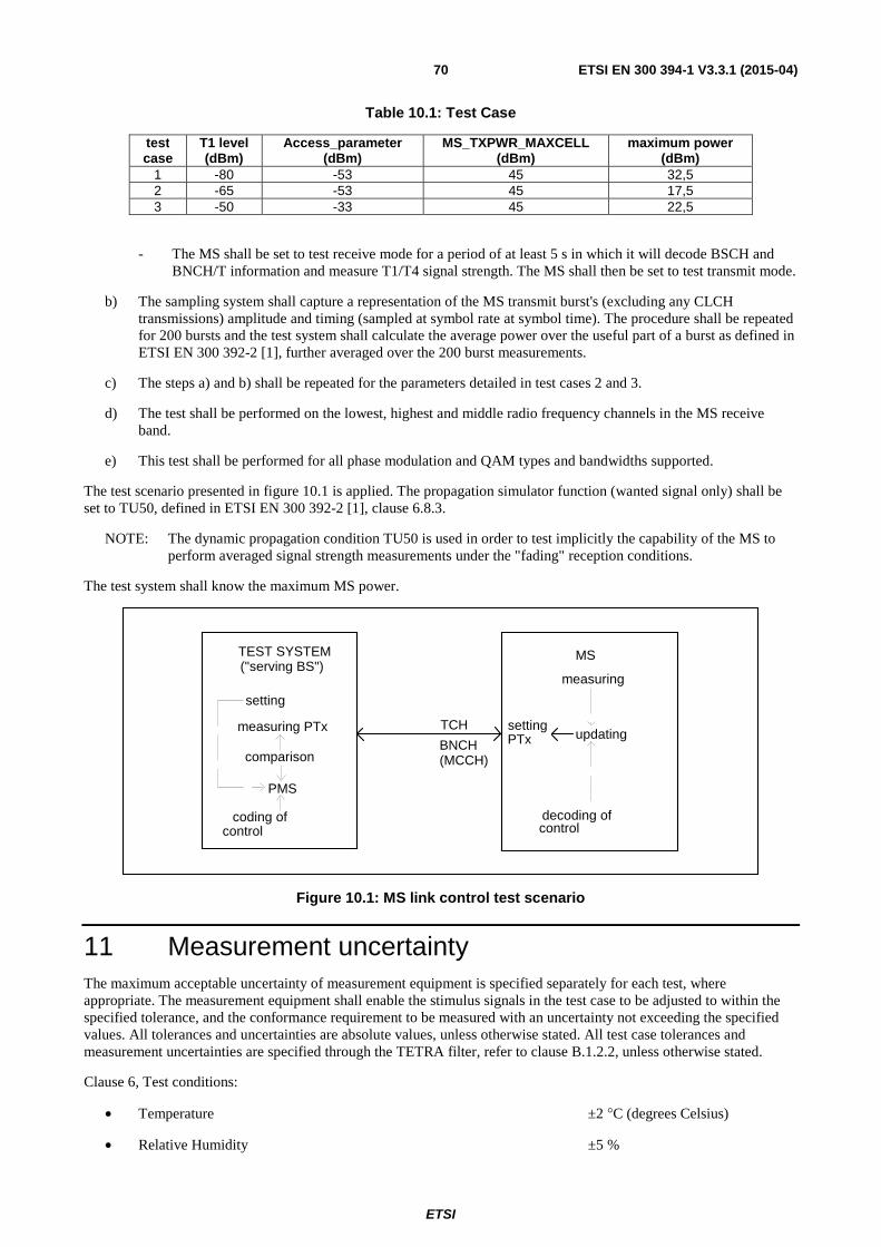
ETSI
ETSI EN 300 394-1 V3.3.1 (2015-04)70
Table 10.1: Test Case
test case
T1 level (dBm)
Access_parameter (dBm)
MS_TXPWR_MAXCELL (dBm)
maximum power (dBm)
1 -80 -53 45 32,5 2 -65 -53 45 17,5 3 -50 -33 45 22,5
- The MS shall be set to test receive mode for a period of at least 5 s in which it will decode BSCH and BNCH/T information and measure T1/T4 signal strength. The MS shall then be set to test transmit mode.
b) The sampling system shall capture a representation of the MS transmit burst's (excluding any CLCH transmissions) amplitude and timing (sampled at symbol rate at symbol time). The procedure shall be repeated for 200 bursts and the test system shall calculate the average power over the useful part of a burst as defined in ETSI EN 300 392-2 [1], further averaged over the 200 burst measurements.
c) The steps a) and b) shall be repeated for the parameters detailed in test cases 2 and 3.
d) The test shall be performed on the lowest, highest and middle radio frequency channels in the MS receive band.
e) This test shall be performed for all phase modulation and QAM types and bandwidths supported.
The test scenario presented in figure 10.1 is applied. The propagation simulator function (wanted signal only) shall be set to TU50, defined in ETSI EN 300 392-2 [1], clause 6.8.3.
NOTE: The dynamic propagation condition TU50 is used in order to test implicitly the capability of the MS to perform averaged signal strength measurements under the "fading" reception conditions.
The test system shall know the maximum MS power.
TEST SYSTEM MS("serving BS")
setting
measuring PTx
comparison
PMS
coding ofcontrol
measuring
updating
decoding ofcontrol
settingPTx
TCH
BNCH(MCCH)
Figure 10.1: MS link control test scenario
11 Measurement uncertainty The maximum acceptable uncertainty of measurement equipment is specified separately for each test, where appropriate. The measurement equipment shall enable the stimulus signals in the test case to be adjusted to within the specified tolerance, and the conformance requirement to be measured with an uncertainty not exceeding the specified values. All tolerances and uncertainties are absolute values, unless otherwise stated. All test case tolerances and measurement uncertainties are specified through the TETRA filter, refer to clause B.1.2.2, unless otherwise stated.
Clause 6, Test conditions:
• Temperature ±2 °C (degrees Celsius)
• Relative Humidity ±5 %
ETSI
ETSI EN 300 394-1 V3.3.1 (2015-04)71
• DC Voltage ±1,0 %
• AC Voltage ±1,5 %
The above values shall apply unless the test environment is controlled and the specification for the control of the test environment specifies the uncertainty for the parameter.
11.1 Transmitter Clause 8.1.1, MS Mean transmitted RF carrier power:
• Test case:
- T1/T4 level ±3,0 dB
• Conformance requirement:
- RF power ±0,75 dB
Clause 8.1.1, MS Transmitted RF carrier power versus time:
• Test case:
- T1/T4 level ±3,0 dB
- Inherent noise level:
- RF power (Lmin) ≤ -80 dBc
• Conformance requirement:
- RF power relative to 0 dB reference (0 dBc to -45 dBc) ±1,0 dB
- RF power relative to 0 dB reference (< -45 dBc to -73 dBc) ±1,5 dB
- Timing uncertainty (profile) ±1/16 symbol
Clause 8.1.2, BS Mean transmitted RF carrier power:
• Test case:
- T1/T4 level ±3,0 dB
• Conformance requirement:
- RF power ±0,75 dB
Clause 8.1.2, BS transmitted RF carrier power versus time:
• Test case:
- T1/T4 level ±3,0 dB
• Inherent noise level:
- RF power (Lmin) ≤ -50 dBc
• Conformance requirement:
- RF power relative to 0 dB reference (0 dBc to -45 dBc) ±1,0 dB
- RF power relative to 0 dB reference (< -45 dBc to -73 dBc) ±1,5 dB
- Timing uncertainty (profile) ±1/16 symbol

ETSI
ETSI EN 300 394-1 V3.3.1 (2015-04)72
Clause 8.2, Unwanted output power in non-active transmit state:
• Test case:
- T1/T4 level ±3,0 dB
• Conformance requirement:
- RF power relative to 0 dB reference (0 dBc to -45 dBc) ±1,0 dB
- RF power relative to 0 dB reference (< -45 dBc to -73 dBc) ±1,5 dB
- Inherent noise level ≤ -80 dBc
Clause 8.3, Adjacent channel power due to modulation:
• Test case:
- T1/T4 level ±3,0 dB
Maximum residual adjacent channel level of the test system:
• For a 25 kHz channel:
- Maximum level at frequency offset 25 kHz -70 dBc
- Maximum level at frequency offset 50 kHz -80 dBc
- Maximum level at frequency offset 75 kHz -80 dBc
• For a 50 kHz channel:
- Maximum level at frequency offset 37,5 kHz -65 dBc
- Maximum level at frequency offset 62,5 kHz -73 dBc
- Maximum level at frequency offset 87,5 kHz -75 dBc
• For a 100 kHz channel:
- Maximum level at frequency offset 62,5 kHz -73 dBc
- Maximum level at frequency offset 87,5 kHz -75 dBc
- Maximum level at frequency offset 112,5 kHz -70 dBc
• For a 150 kHz channel:
- Maximum level at frequency offset 87,5 kHz -75 dBc
- Maximum level at frequency offset 112,5 kHz -70 dBc
- Maximum level at frequency offset 137,5 kHz -70 dBc
• Conformance requirement:
- RF power (0 dB reference) ±1,0 dB
- RF power relative to 0 dB reference (0 dBc to -45 dBc) ±1,0 dB
- RF power relative to 0 dB reference (< -45 dBc to -73 dBc) ±1,5 dB
- RF power (absolute limit values) ±1,0 dB

ETSI
ETSI EN 300 394-1 V3.3.1 (2015-04)73
Clause 8.4, Adjacent channel power due to switching transients:
• Test case:
- T1/T4 level ±3,0 dB
Maximum residual adjacent channel level of the test system:
• For a 25 kHz channel:
- Maximum level at frequency offset 25 kHz -60 dBc
• For a 50 kHz channel:
- Maximum level at frequency offset 37,5 kHz -60 dBc
• For a 100 kHz channel:
- Maximum level at frequency offset 62,5 kHz -60 dBc
• For a 150 kHz channel:
- Maximum level at frequency offset 87,5 kHz -60 dBc
• Conformance requirement:
- RF power (0 dB reference) ±1,0 dB
- RF power relative to 0 dB reference (0 dBc to -45 dBc) ±1,0 dB
- RF power relative to 0 dB reference (< -45 dBc to -53 dBc) ±1,5 dB
Clause 8.5, Unwanted emissions far from the carrier; a) discrete spurious:
• Test case:
- T1/T4 level ±3,0 dB
• Conformance requirement:
- RF power (offsets within frb) ±1,5 dB
- RF power (offsets > frb, not TETRA filtered):
� f ≤ 1 GHz ±1,5 dB
� 1 GHz < f ≤ 2 GHz ±2,0 dB
� 2 GHz < f ≤ 4 GHz ±3,0 dB
� 4 GHz < f ≤ 12,75 GHz ±4,0 dB
Clause 8.5, Unwanted emissions far from the carrier; b) wideband noise:
• Test case:
- T1/T4 level ±3,0 dB
• Conformance requirement:
- RF power relative to 0 dB reference (0 dBc to - 45 dBc) ±1,0 dB
- RF power relative to 0 dB reference (< -45 dBc to -105 dBc) ±1,5 dB
ETSI
ETSI EN 300 394-1 V3.3.1 (2015-04)74
Clause 8.6, Unwanted radiated emissions:
• Test case:
- T1/T4 level (conducted) ±3,0 dB
• Conformance requirement:
- RF power (not TETRA filtered) ±4,0 dB
Clause 8.7, Unwanted emissions during the BLCH/CLCH (linearization):
• Test case:
- T1/T4 level ±3,0 dB
• Conformance requirement:
- RF power (0 dB reference) ±1,0 dB
- RF power relative to 0 dB reference (0 dBc to -45 dBc) ±1,0 dB
- RF power relative to 0 dB reference (< -45 dBc to -73 dBc) ±1,5 dB
Clause 8.8, Tx intermodulation attenuation:
• Test case:
- T1/T4 level ±3,0 dB
- T3 level (not TETRA filtered), relative to RF power ±1,0 dB
• Conformance requirement:
- RF power (0 dB reference) ±1,0 dB
- RF power (note) relative to 0 dB reference (0 dBc to -45 dBc) ±1,0 dB
- RF power (note) relative to 0 dB ref. (< -45 dBc to -73 dBc) ±1,5 dB
NOTE: Not TETRA filtered.
11.2 Receiver Where a measurement uncertainty of + x, x dB / 0,0 dB is specified for an input signal, the measured value of the input signal should be increased by an amount equal to the uncertainty with which it can be measured. This will ensure that the true value of the input signal is not below the specified nominal.
Clause 9.2, Nominal error rates:
• Test case:
- T1/T4 level, static ±1,0 dB
- T1/T4 level, dynamic ±1,5 dB
Clause 9.3, Reference sensitivity performance:
• Test case:
- T1/T4 level, dynamic +3,0 dB / -0,0 dB
Clause 9.4, Reference interference performance:
• Test case:
- T1/T4 level, dynamic +3,0 dB / -0,0 dB
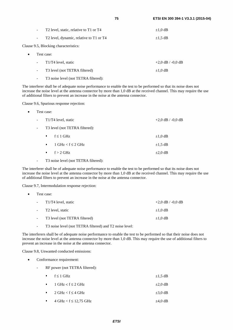
ETSI
ETSI EN 300 394-1 V3.3.1 (2015-04)75
- T2 level, static, relative to T1 or T4 ±1,0 dB
- T2 level, dynamic, relative to T1 or T4 ±1,5 dB
Clause 9.5, Blocking characteristics:
• Test case:
- T1/T4 level, static +2,0 dB / -0,0 dB
- T3 level (not TETRA filtered) ±1,0 dB
- T3 noise level (not TETRA filtered):
The interferer shall be of adequate noise performance to enable the test to be performed so that its noise does not increase the noise level at the antenna connector by more than 1,0 dB at the received channel. This may require the use of additional filters to prevent an increase in the noise at the antenna connector.
Clause 9.6, Spurious response rejection:
• Test case:
- T1/T4 level, static +2,0 dB / -0,0 dB
- T3 level (not TETRA filtered):
� f ≤ 1 GHz ±1,0 dB
� 1 GHz < f ≤ 2 GHz ±1,5 dB
� f > 2 GHz ±2,0 dB
- T3 noise level (not TETRA filtered):
The interferer shall be of adequate noise performance to enable the test to be performed so that its noise does not increase the noise level at the antenna connector by more than 1,0 dB at the received channel. This may require the use of additional filters to prevent an increase in the noise at the antenna connector.
Clause 9.7, Intermodulation response rejection:
• Test case:
- T1/T4 level, static +2,0 dB / -0,0 dB
- T2 level, static ±1,0 dB
- T3 level (not TETRA filtered) ±1,0 dB
- T3 noise level (not TETRA filtered) and T2 noise level:
The interferers shall be of adequate noise performance to enable the test to be performed so that their noise does not increase the noise level at the antenna connector by more than 1,0 dB. This may require the use of additional filters to prevent an increase in the noise at the antenna connector.
Clause 9.8, Unwanted conducted emissions:
• Conformance requirement:
- RF power (not TETRA filtered):
� f ≤ 1 GHz ±1,5 dB
� 1 GHz < f ≤ 2 GHz ±2,0 dB
� 2 GHz < f ≤ 4 GHz ±3,0 dB
� 4 GHz < f ≤ 12,75 GHz ±4,0 dB
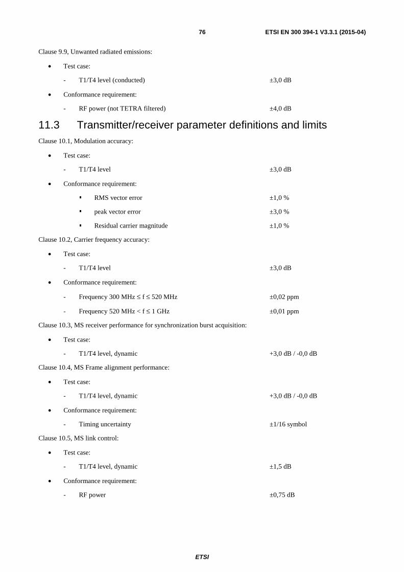
ETSI
ETSI EN 300 394-1 V3.3.1 (2015-04)76
Clause 9.9, Unwanted radiated emissions:
• Test case:
- T1/T4 level (conducted) ±3,0 dB
• Conformance requirement:
- RF power (not TETRA filtered) ±4,0 dB
11.3 Transmitter/receiver parameter definitions and limits Clause 10.1, Modulation accuracy:
• Test case:
- T1/T4 level ±3,0 dB
• Conformance requirement:
� RMS vector error ±1,0 %
� peak vector error ±3,0 %
� Residual carrier magnitude ±1,0 %
Clause 10.2, Carrier frequency accuracy:
• Test case:
- T1/T4 level ±3,0 dB
• Conformance requirement:
- Frequency 300 MHz ≤ f ≤ 520 MHz ±0,02 ppm
- Frequency 520 MHz < f ≤ 1 GHz ±0,01 ppm
Clause 10.3, MS receiver performance for synchronization burst acquisition:
• Test case:
- T1/T4 level, dynamic +3,0 dB / -0,0 dB
Clause 10.4, MS Frame alignment performance:
• Test case:
- T1/T4 level, dynamic +3,0 dB / -0,0 dB
• Conformance requirement:
- Timing uncertainty ±1/16 symbol
Clause 10.5, MS link control:
• Test case:
- T1/T4 level, dynamic ±1,5 dB
• Conformance requirement:
- RF power ±0,75 dB

ETSI
ETSI EN 300 394-1 V3.3.1 (2015-04)77
11.4 Interpretation of measurement results The measurement value related to the corresponding limit shall be used to decide whether equipment meets a requirement in the present document. The measurement uncertainty for the measurement of each parameter shall be included in the test report. The recorded value for the measurement uncertainty shall be, for each measurement, equal to or lower than the appropriate value in clause 11 of the present document.
NOTE: This procedure is recommended in ETSI ETR 028 [i.1].

ETSI
ETSI EN 300 394-1 V3.3.1 (2015-04)78
Annex A (normative): TETRA receiver testing
A.1 Frequencies of spurious response Annex A provides a definition of the interfering frequencies which are used during measurement of the spurious response rejection.
The interfering frequencies which are used during measurement of the spurious response rejection are defined as the combined frequencies of two sets of frequencies:
a) All frequencies (fl) in integer steps of the bandwidth of the signal divided by four and within the limited frequency range:
f f sr f f f sr lo ij
j
n l lo ij
j
n − − ∑ ≤ ≤ + +∑
= =1 1 2 2
Where (sr) is the switching range of the receive band of the equipment, (flo) is the frequency of the local oscillator signal applied to the first mixer of the receiver and (fi1,...,fin) is the intermediate frequencies of the receiver.
b) The discrete frequencies at which spurious response can occur outside the range determined in a) above for the remainder of the frequency range of interest up to 4 GHz determined as nflo ± fi1 and pfr ± fi1, where n is an integer greater than or equal to 2, p is an integer greater than or equal to 1, (fr) is the frequency of any other oscillator used to generate reference frequencies in the receiver and (fi1) is the first intermediate frequencies of the receiver.
For the calculations a) and b) above, the manufacturer shall state the frequency of the receiver (f0), the frequency of the
local oscillator signal (flo) applied to the 1st mixer of the receiver, the frequency (fr) of any other oscillator used to
generate reference frequencies in the receiver, the intermediate frequencies (fi1,..., fin) and the switching range (sr) of
the receiver (ETSI EN 300 392-2 [1]).
A.2 Test cases and test conditions for BS and MS receivers
Annex A contains receiver test tables A.1 to A.18 for TETRA BS and MS equipment for V+D applications. The tables list test type and provide information on channel type used in each test, test limits, minimum sample size and signal levels. Only in the case where a MS or BS supports protected circuit mode data shall the TCH/2,4 receiver sensitivity measurements be conducted. Test specifications and limits which are bold indicate a BER measurement and those which are not, are MER or FER measurements. For those tests measured under both normal and extreme test conditions, signal levels under extreme test conditions are shown in brackets, "( )". Test tables for PUEM measurements are given at the end of the annex. The propagation models specified (TU50, HT200, EQ200) are defined in ETSI EN 300 392-2 [1], clause 6.8.3. The minimum sample size is determined from the following equation, from ETSI ETR 028 [i.1].
NOTE: The minimum number of samples refers to the number of bits for BER measurements and number of frames or messages for FER and MER measurements.
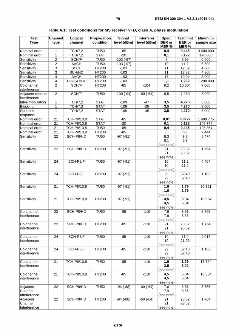
ETSI
ETSI EN 300 394-1 V3.3.1 (2015-04)79
Table A.1: Test conditions for MS receiver V+D, class A, phase modulation
Test Type
Channel type
Logical channel
Propagation condition
Signal level (dBm)
Interferer level (dBm)
Spec. BER or MER %
Test limit BER or MER %
Minimum sample size
Nominal error 1 TCH/7,2 TU50 -85 0,4 0,448 3 600 000 Nominal error 1 TCH/7,2 STAT -20 0,1 0,122 170 000 Sensitivity 2 SCH/F TU50 -103 (-97) 8 8,96 6 600 Sensitivity 2 AACH TU50 -103 (-97) 10 11,2 6 600 Sensitivity 3 BSCH HT200 -103 11 12,32 4 800 Sensitivity 3 SCH/HD HT200 -103 11 12,32 4 800 Sensitivity 4 AACH HT200 -103 17 19,04 3 000 Sensitivity 4 TCH/2,4 N = 1 HT200 -103 1,1 1,232 1 290 000 Co-channel interference
2 SCH/F HT200 -85 -104 9,2 10,304 7 000
Adjacent channel interference
2 SCH/F TU50 -100 (-94) -60 (-64) 6,5 7,280 8 000
Inter-modulation 1 TCH/7,2 STAT -109 -47 3,5 4,270 5 000 Blocking 1 TCH/7,2 STAT -109 -25 3,5 4,270 5 000 Spurious response
1 TCH/7,2 STAT -109 -45 3,5 4,270 5 000
Nominal error 21 TCH-P8/10,8 STAT -85 0,01 0,0122 1 499 775 Nominal error 21 TCH-P8/10,8 STAT -20 0,1 0,122 149 774 Nominal error 21 TCH-P8/10,8 TU50 -85 0,4 0,448 125 364 Nominal error 21 TCH-P8/10,8 HT200 -85 5 5,6 9 444 Sensitivity 22 SCH-P8/HD TU50 -97 (-91) 8,3
8,1 (see note)
9,3 9,3
5 474
Sensitivity 22 SCH-P8/HD HT200 -97 (-91) 21 21
(see note)
23,52 23,52
1 764
Sensitivity 24 SCH-P8/F TU50 -97 (-91) 10 10
(see note)
11,2 11,2
4 404
Sensitivity 24 SCH-P8/F HT200 -97 (-91) 29 29
(see note)
32,48 32,48
1 102
Sensitivity 21 TCH-P8/10,8 TU50 -97 (-91) 1,6 1,6
(see note)
1,79 1,79
30 321
Sensitivity 21 TCH-P8/10,8 HT200 -97 (-91) 4,5 4,5
(see note)
5,04 5,04
10 564
Co-channel interference
22 SCH-P8/HD TU50 -85 -110 7,6 7,9
(see note)
8,51 8,85
5 765
Co-channel interference
22 SCH-P8/HD HT200 -85 -110 21 21
(see note)
23,52 23,52
1 764
Co-channel interference
24 SCH-P8/F TU50 -85 -110 10 19
(see note)
11,2 21,28
2 017
Co-channel interference
24 SCH-P8/F HT200 -85 -110 29 29
(see note)
32,48 32,48
1 102
Co-channel interference
21 TCH-P8/10,8 TU50 -85 -110 1,6 3,5
(see note)
1,79 3,92
13 764
Co-channel interference
21 TCH-P8/10,8 HT200 -85 -110 4,5 4,5
(see note)
5,04 5,04
10 564
Adjacent Channel Interference
22 SCH-P8/HD TU50 -94 (-88) -60 (-64) 7,6 7,9
(see note)
8,51 8,85
5 765
Adjacent Channel Interference
22 SCH-P8/HD HT200 -94 (-88) -60 (-64) 21 21
(see note)
23,52 23,52
1 764
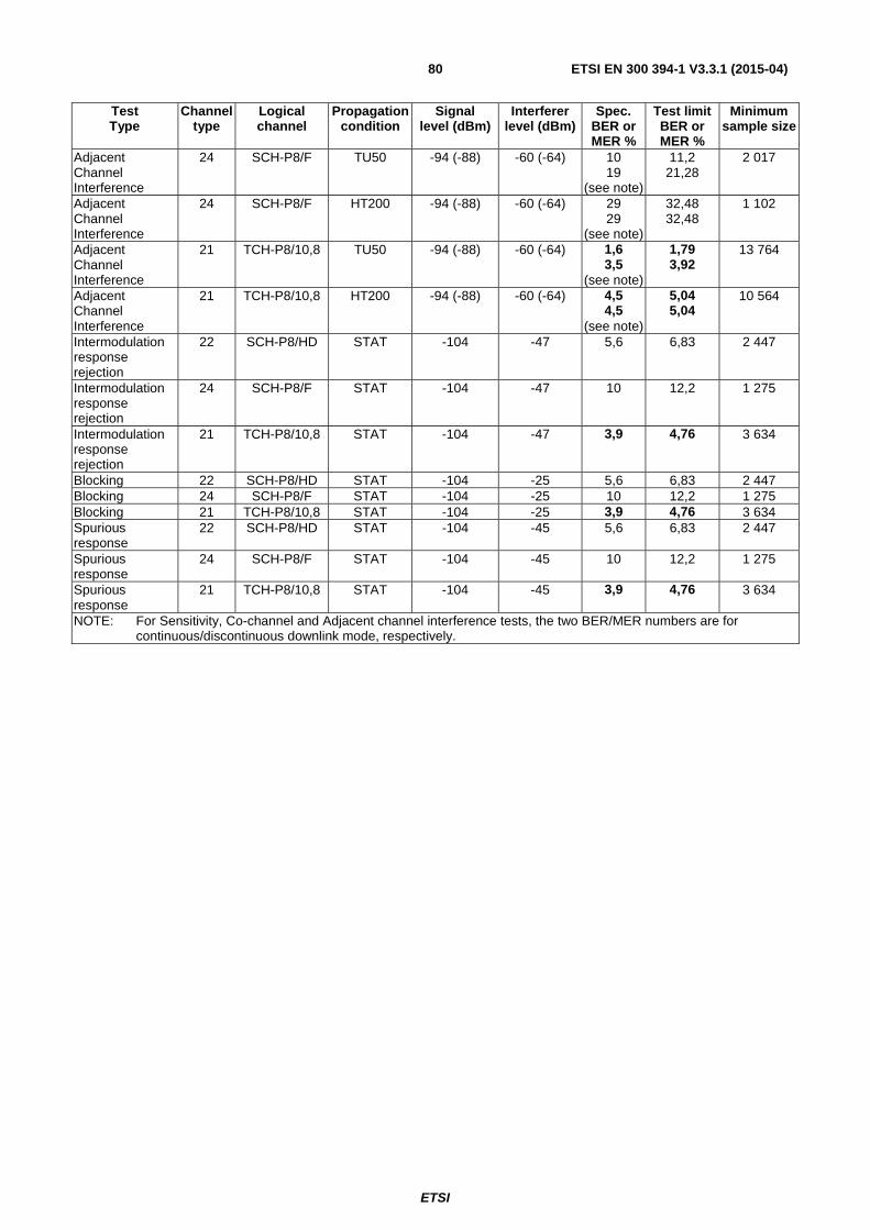
ETSI
ETSI EN 300 394-1 V3.3.1 (2015-04)80
Test Type
Channel type
Logical channel
Propagation condition
Signal level (dBm)
Interferer level (dBm)
Spec. BER or MER %
Test limit BER or MER %
Minimum sample size
Adjacent Channel Interference
24 SCH-P8/F TU50 -94 (-88) -60 (-64) 10 19
(see note)
11,2 21,28
2 017
Adjacent Channel Interference
24 SCH-P8/F HT200 -94 (-88) -60 (-64) 29 29
(see note)
32,48 32,48
1 102
Adjacent Channel Interference
21 TCH-P8/10,8 TU50 -94 (-88) -60 (-64) 1,6 3,5
(see note)
1,79 3,92
13 764
Adjacent Channel Interference
21 TCH-P8/10,8 HT200 -94 (-88) -60 (-64) 4,5 4,5
(see note)
5,04 5,04
10 564
Intermodulation response rejection
22 SCH-P8/HD STAT -104 -47 5,6 6,83 2 447
Intermodulation response rejection
24 SCH-P8/F STAT -104 -47 10 12,2 1 275
Intermodulation response rejection
21 TCH-P8/10,8 STAT -104 -47 3,9 4,76 3 634
Blocking 22 SCH-P8/HD STAT -104 -25 5,6 6,83 2 447 Blocking 24 SCH-P8/F STAT -104 -25 10 12,2 1 275 Blocking 21 TCH-P8/10,8 STAT -104 -25 3,9 4,76 3 634 Spurious response
22 SCH-P8/HD STAT -104 -45 5,6 6,83 2 447
Spurious response
24 SCH-P8/F STAT -104 -45 10 12,2 1 275
Spurious response
21 TCH-P8/10,8 STAT -104 -45 3,9 4,76 3 634
NOTE: For Sensitivity, Co-channel and Adjacent channel interference tests, the two BER/MER numbers are for continuous/discontinuous downlink mode, respectively.
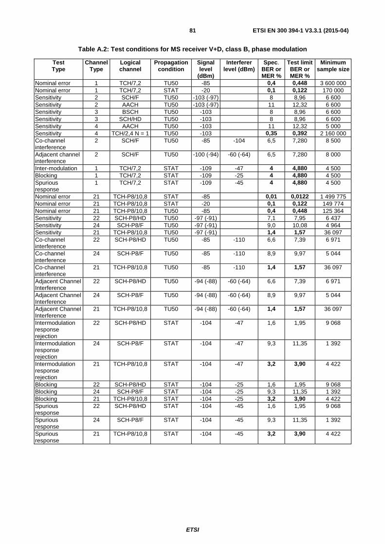
ETSI
ETSI EN 300 394-1 V3.3.1 (2015-04)81
Table A.2: Test conditions for MS receiver V+D, class B, phase modulation
Test Type
Channel Type
Logical channel
Propagation condition
Signal level
(dBm)
Interferer level (dBm)
Spec. BER or MER %
Test limit BER or MER %
Minimum sample size
Nominal error 1 TCH/7,2 TU50 -85 0,4 0,448 3 600 000 Nominal error 1 TCH/7,2 STAT -20 0,1 0,122 170 000 Sensitivity 2 SCH/F TU50 -103 (-97) 8 8,96 6 600 Sensitivity 2 AACH TU50 -103 (-97) 11 12,32 6 600 Sensitivity 3 BSCH TU50 -103 8 8,96 6 600 Sensitivity 3 SCH/HD TU50 -103 8 8,96 6 600 Sensitivity 4 AACH TU50 -103 11 12,32 5 000 Sensitivity 4 TCH/2,4 N = 1 TU50 -103 0,35 0,392 2 160 000 Co-channel interference
2 SCH/F TU50 -85 -104 6,5 7,280 8 500
Adjacent channel interference
2 SCH/F TU50 -100 (-94) -60 (-64) 6,5 7,280 8 000
Inter-modulation 1 TCH/7,2 STAT -109 -47 4 4,880 4 500 Blocking 1 TCH/7,2 STAT -109 -25 4 4,880 4 500 Spurious response
1 TCH/7,2 STAT -109 -45 4 4,880 4 500
Nominal error 21 TCH-P8/10,8 STAT -85 0,01 0,0122 1 499 775 Nominal error 21 TCH-P8/10,8 STAT -20 0,1 0,122 149 774 Nominal error 21 TCH-P8/10,8 TU50 -85 0,4 0,448 125 364 Sensitivity 22 SCH-P8/HD TU50 -97 (-91) 7,1 7,95 6 437 Sensitivity 24 SCH-P8/F TU50 -97 (-91) 9,0 10,08 4 964 Sensitivity 21 TCH-P8/10,8 TU50 -97 (-91) 1,4 1,57 36 097 Co-channel interference
22 SCH-P8/HD TU50 -85 -110
6,6 7,39 6 971
Co-channel interference
24 SCH-P8/F TU50 -85 -110 8,9 9,97 5 044
Co-channel interference
21 TCH-P8/10,8 TU50 -85 -110 1,4 1,57 36 097
Adjacent Channel Interference
22 SCH-P8/HD TU50 -94 (-88) -60 (-64) 6,6 7,39 6 971
Adjacent Channel Interference
24 SCH-P8/F TU50 -94 (-88) -60 (-64) 8,9 9,97 5 044
Adjacent Channel Interference
21 TCH-P8/10,8 TU50 -94 (-88) -60 (-64) 1,4 1,57 36 097
Intermodulation response rejection
22 SCH-P8/HD STAT -104 -47 1,6 1,95 9 068
Intermodulation response rejection
24 SCH-P8/F STAT -104 -47 9,3 11,35 1 392
Intermodulation response rejection
21 TCH-P8/10,8 STAT -104 -47 3,2 3,90 4 422
Blocking 22 SCH-P8/HD STAT -104 -25 1,6 1,95 9 068 Blocking 24 SCH-P8/F STAT -104 -25 9,3 11,35 1 392 Blocking 21 TCH-P8/10,8 STAT -104 -25 3,2 3,90 4 422 Spurious response
22 SCH-P8/HD STAT -104 -45 1,6 1,95 9 068
Spurious response
24 SCH-P8/F STAT -104 -45 9,3 11,35 1 392
Spurious response
21 TCH-P8/10,8 STAT -104 -45 3,2 3,90 4 422
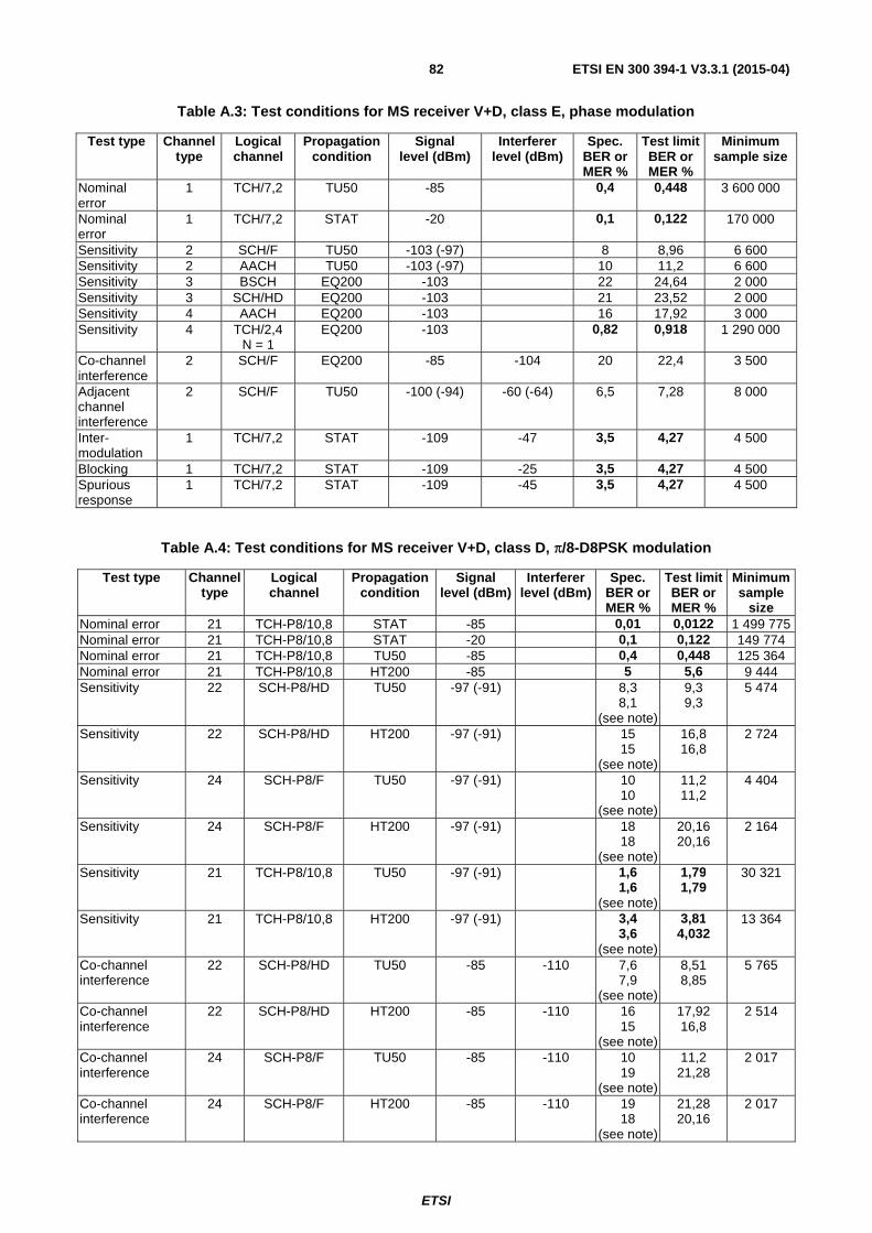
ETSI
ETSI EN 300 394-1 V3.3.1 (2015-04)82
Table A.3: Test conditions for MS receiver V+D, class E, phase modulation
Test type Channel type
Logical channel
Propagation condition
Signal level (dBm)
Interferer level (dBm)
Spec. BER or MER %
Test limit BER or MER %
Minimum sample size
Nominal error
1 TCH/7,2 TU50 -85 0,4 0,448 3 600 000
Nominal error
1 TCH/7,2 STAT -20 0,1 0,122 170 000
Sensitivity 2 SCH/F TU50 -103 (-97) 8 8,96 6 600 Sensitivity 2 AACH TU50 -103 (-97) 10 11,2 6 600 Sensitivity 3 BSCH EQ200 -103 22 24,64 2 000 Sensitivity 3 SCH/HD EQ200 -103 21 23,52 2 000 Sensitivity 4 AACH EQ200 -103 16 17,92 3 000 Sensitivity 4 TCH/2,4
N = 1 EQ200 -103 0,82 0,918 1 290 000
Co-channel interference
2 SCH/F EQ200 -85 -104 20 22,4 3 500
Adjacent channel interference
2 SCH/F TU50 -100 (-94) -60 (-64) 6,5 7,28 8 000
Inter-modulation
1 TCH/7,2 STAT -109 -47 3,5 4,27 4 500
Blocking 1 TCH/7,2 STAT -109 -25 3,5 4,27 4 500 Spurious response
1 TCH/7,2 STAT -109 -45 3,5 4,27 4 500
Table A.4: Test conditions for MS receiver V+D, class D, π/8-D8PSK modulation
Test type Channel type
Logical channel
Propagation condition
Signal level (dBm)
Interferer level (dBm)
Spec. BER or MER %
Test limit BER or MER %
Minimum sample
size Nominal error 21 TCH-P8/10,8 STAT -85 0,01 0,0122 1 499 775 Nominal error 21 TCH-P8/10,8 STAT -20 0,1 0,122 149 774 Nominal error 21 TCH-P8/10,8 TU50 -85 0,4 0,448 125 364 Nominal error 21 TCH-P8/10,8 HT200 -85 5 5,6 9 444 Sensitivity 22 SCH-P8/HD TU50 -97 (-91) 8,3
8,1 (see note)
9,3 9,3
5 474
Sensitivity 22 SCH-P8/HD HT200 -97 (-91) 15 15
(see note)
16,8 16,8
2 724
Sensitivity 24 SCH-P8/F TU50 -97 (-91) 10 10
(see note)
11,2 11,2
4 404
Sensitivity 24 SCH-P8/F HT200 -97 (-91) 18 18
(see note)
20,16 20,16
2 164
Sensitivity 21 TCH-P8/10,8 TU50 -97 (-91) 1,6 1,6
(see note)
1,79 1,79
30 321
Sensitivity 21 TCH-P8/10,8 HT200 -97 (-91) 3,4 3,6
(see note)
3,81 4,032
13 364
Co-channel interference
22 SCH-P8/HD TU50 -85 -110 7,6 7,9
(see note)
8,51 8,85
5 765
Co-channel interference
22 SCH-P8/HD HT200 -85 -110 16 15
(see note)
17,92 16,8
2 514
Co-channel interference
24 SCH-P8/F TU50 -85 -110 10 19
(see note)
11,2 21,28
2 017
Co-channel interference
24 SCH-P8/F HT200 -85 -110 19 18
(see note)
21,28 20,16
2 017
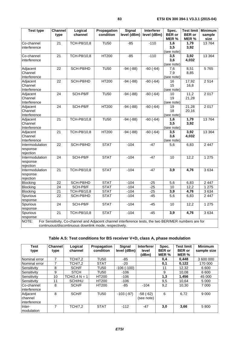
ETSI
ETSI EN 300 394-1 V3.3.1 (2015-04)83
Test type Channel type
Logical channel
Propagation condition
Signal level (dBm)
Interferer level (dBm)
Spec. BER or MER %
Test limit BER or MER %
Minimum sample
size Co-channel interference
21 TCH-P8/10,8 TU50 -85 -110 1,6 3,5
(see note)
1,79 3,92
13 764
Co-channel interference
21 TCH-P8/10,8 HT200 -85 -110 3,5 3,6
(see note)
3,92 4,032
13 364
Adjacent Channel Interference
22 SCH-P8/HD TU50 -94 (-88) -60 (-64) 7,6 7,9
(see note)
8,51 8,85
5 765
Adjacent Channel Interference
22 SCH-P8/HD HT200 -94 (-88) -60 (-64) 16 15
(see note)
17,92 16,8
2 514
Adjacent Channel Interference
24 SCH-P8/F TU50 -94 (-88) -60 (-64) 10 19
(see note)
11,2 21,28
2 017
Adjacent Channel Interference
24 SCH-P8/F HT200 -94 (-88) -60 (-64) 19 18
(see note)
21,28 20,16
2 017
Adjacent Channel Interference
21 TCH-P8/10,8 TU50 -94 (-88) -60 (-64) 1,6 3,5
(see note)
1,79 3,92
13 764
Adjacent Channel Interference
21 TCH-P8/10,8 HT200 -94 (-88) -60 (-64) 3,5 3,6
(see note)
3,92 4,032
13 364
Intermodulation response rejection
22 SCH-P8/HD STAT -104 -47 5,6 6,83 2 447
Intermodulation response rejection
24 SCH-P8/F STAT -104 -47 10 12,2 1 275
Intermodulation response rejection
21 TCH-P8/10,8 STAT -104 -47 3,9 4,76 3 634
Blocking 22 SCH-P8/HD STAT -104 -25 5,6 6,83 2 447 Blocking 24 SCH-P8/F STAT -104 -25 10 12,2 1 275 Blocking 21 TCH-P8/10,8 STAT -104 -25 3,9 4,76 3 634 Spurious response
22 SCH-P8/HD STAT -104 -45 5,6 6,83 2 447
Spurious response
24 SCH-P8/F STAT -104 -45 10 12,2 1 275
Spurious response
21 TCH-P8/10,8 STAT -104 -45 3,9 4,76 3 634
NOTE: For Sensitivity, Co-channel and Adjacent channel interference tests, the two BER/MER numbers are for continuous/discontinuous downlink mode, respectively.
Table A.5: Test conditions for BS receiver V+D, class A, phase modulation
Test type
Channel type
Logical channel
Propagation condition
Signal level (dBm)
Interferer level
(dBm)
Spec. BER or MER %
Test limit BER or MER %
Minimum sample size
Nominal error 7 TCH/7,2 TU50 -85 0,4 0,448 3 600 000 Nominal error 7 TCH/7,2 STAT -20 0,1 0,122 170 000 Sensitivity 8 SCH/F TU50 -106 (-100) 11 12,32 6 600 Sensitivity 9 STCH TU50 -106 9 10,08 6 600 Sensitivity 10 TCH/2,4 N = 1 HT200 -106 1,3 1,456 45 000 Sensitivity 11 SCH/HU HT200 -106 9,5 10,64 5 000 Co-channel interference
8 SCH/F HT200 -85 -104 9,2 10,30 7 000
Adjacent channel interference
8 SCH/F TU50 -103 (-97) -58 (-62) (see note)
6 6,72 9 000
Inter-modulation
7 TCH/7,2 STAT -112 -47 3,0 3,66 5 800
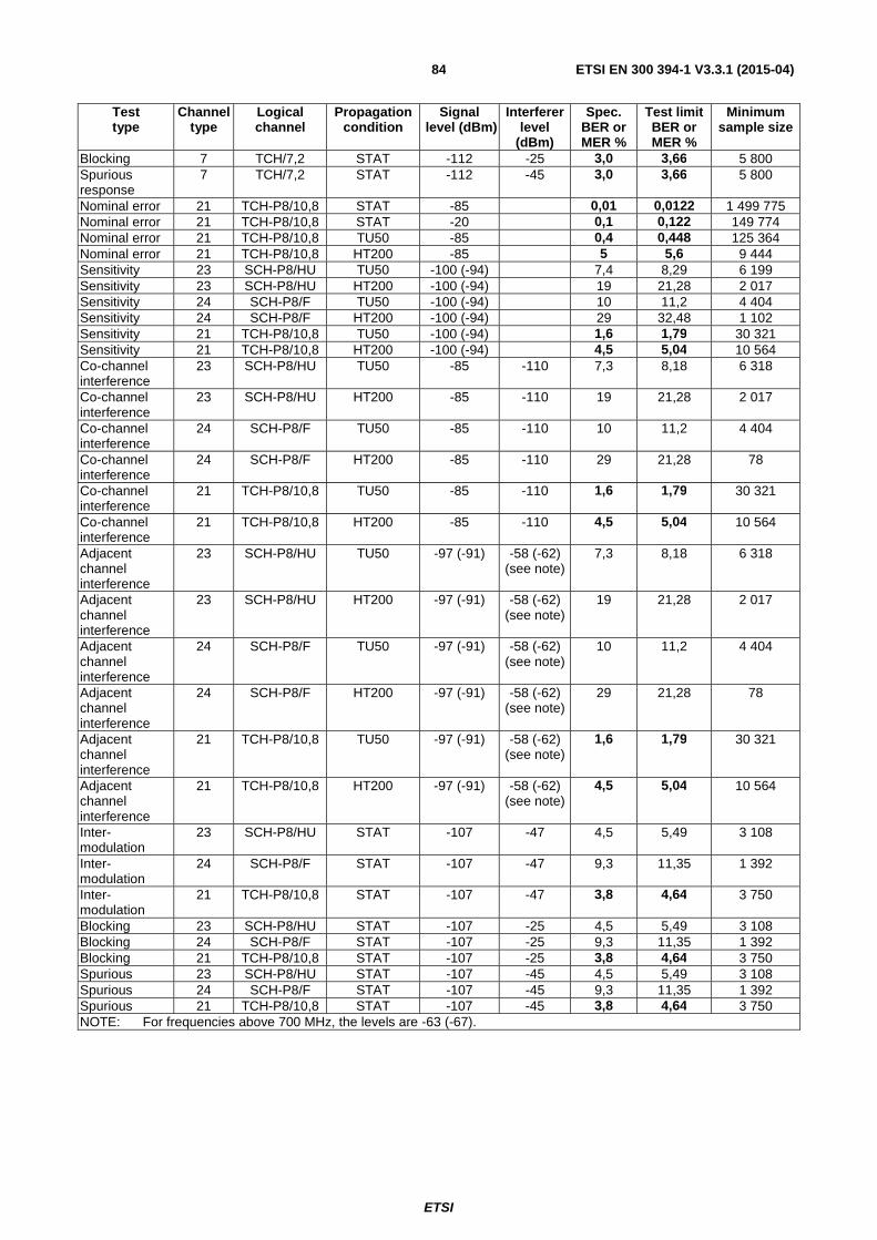
ETSI
ETSI EN 300 394-1 V3.3.1 (2015-04)84
Test type
Channel type
Logical channel
Propagation condition
Signal level (dBm)
Interferer level
(dBm)
Spec. BER or MER %
Test limit BER or MER %
Minimum sample size
Blocking 7 TCH/7,2 STAT -112 -25 3,0 3,66 5 800 Spurious response
7 TCH/7,2 STAT -112 -45 3,0 3,66 5 800
Nominal error 21 TCH-P8/10,8 STAT -85 0,01 0,0122 1 499 775 Nominal error 21 TCH-P8/10,8 STAT -20 0,1 0,122 149 774 Nominal error 21 TCH-P8/10,8 TU50 -85 0,4 0,448 125 364 Nominal error 21 TCH-P8/10,8 HT200 -85 5 5,6 9 444 Sensitivity 23 SCH-P8/HU TU50 -100 (-94) 7,4 8,29 6 199 Sensitivity 23 SCH-P8/HU HT200 -100 (-94) 19 21,28 2 017 Sensitivity 24 SCH-P8/F TU50 -100 (-94) 10 11,2 4 404 Sensitivity 24 SCH-P8/F HT200 -100 (-94) 29 32,48 1 102 Sensitivity 21 TCH-P8/10,8 TU50 -100 (-94) 1,6 1,79 30 321 Sensitivity 21 TCH-P8/10,8 HT200 -100 (-94) 4,5 5,04 10 564 Co-channel interference
23 SCH-P8/HU TU50 -85 -110 7,3 8,18 6 318
Co-channel interference
23 SCH-P8/HU HT200 -85 -110 19 21,28 2 017
Co-channel interference
24 SCH-P8/F TU50 -85 -110 10 11,2 4 404
Co-channel interference
24 SCH-P8/F HT200 -85 -110 29 21,28 78
Co-channel interference
21 TCH-P8/10,8 TU50 -85 -110 1,6 1,79 30 321
Co-channel interference
21 TCH-P8/10,8 HT200 -85 -110 4,5 5,04 10 564
Adjacent channel interference
23 SCH-P8/HU TU50 -97 (-91) -58 (-62) (see note)
7,3 8,18 6 318
Adjacent channel interference
23 SCH-P8/HU HT200 -97 (-91) -58 (-62) (see note)
19 21,28 2 017
Adjacent channel interference
24 SCH-P8/F TU50 -97 (-91) -58 (-62) (see note)
10 11,2 4 404
Adjacent channel interference
24 SCH-P8/F HT200 -97 (-91) -58 (-62) (see note)
29 21,28 78
Adjacent channel interference
21 TCH-P8/10,8 TU50 -97 (-91) -58 (-62) (see note)
1,6 1,79 30 321
Adjacent channel interference
21 TCH-P8/10,8 HT200 -97 (-91) -58 (-62) (see note)
4,5 5,04 10 564
Inter-modulation
23 SCH-P8/HU STAT -107 -47 4,5 5,49 3 108
Inter-modulation
24 SCH-P8/F STAT -107 -47 9,3 11,35 1 392
Inter-modulation
21 TCH-P8/10,8 STAT -107 -47 3,8 4,64 3 750
Blocking 23 SCH-P8/HU STAT -107 -25 4,5 5,49 3 108 Blocking 24 SCH-P8/F STAT -107 -25 9,3 11,35 1 392 Blocking 21 TCH-P8/10,8 STAT -107 -25 3,8 4,64 3 750 Spurious 23 SCH-P8/HU STAT -107 -45 4,5 5,49 3 108 Spurious 24 SCH-P8/F STAT -107 -45 9,3 11,35 1 392 Spurious 21 TCH-P8/10,8 STAT -107 -45 3,8 4,64 3 750 NOTE: For frequencies above 700 MHz, the levels are -63 (-67).

ETSI
ETSI EN 300 394-1 V3.3.1 (2015-04)85
Table A.6: Test conditions for BS receiver V+D, class B, phase modulation
Test type
Channel type
Logical channel Propagation condition
Signal level (dBm)
Interferer level
(dBm)
Spec. BER or MER %
Test limit BER or MER %
Minimum sample size
Nominal error 7 TCH/7,2 TU50 -85 0,4 0,448 3 600 000 Nominal error 7 TCH/7,2 STAT -20 0,1 0,122 170 000 Sensitivity 8 SCH/F TU50 -106 (-100) 8 8,96 6 600 Sensitivity 9 STCH TU50 -106 8 8,96 6 600 Sensitivity 10 TCH/2,4 N = 1 TU50 -106 0,35 0,392 160 000 Sensitivity 11 SCH/HU TU50 -106 8 8,96 6 600 Co-channel interference
8 SCH/F TU50 -85 -104 6 6,72 7 000
Adjacent channel interference
8 SCH/F TU50 -103 (-97) -58 (-62) (see note)
6 6,72 9 000
Inter-modulation
7 TCH/7,2 STAT -112 -47 4,0 4,88 4 000
Blocking 7 TCH/7,2 STAT -112 -25 4,0 4,88 4 000 Spurious response
7 TCH/7,2 STAT -112 -45 4,0 4,88 4 000
Nominal error 21 TCH-P8/10,8 STAT -85 0,01 0,0122 1 499 775 Nominal error 21 TCH-P8/10,8 STAT -20 0,1 0,122 149 774 Nominal error 21 TCH-P8/10,8 TU50 -85 0,4 0,448 125 364 Sensitivity 23 SCH-P8/HU TU50 -100 (-94) 6,3 7,06 7 432 Sensitivity 24 SCH-P8/F TU50 -100 (-94) 8,9 9,97 5 044 Sensitivity 21 TCH-P8/10,8 TU50 -100 (-94) 1,4 1,57 36 097 Co-channel interference
23 SCH-P8/HU TU50 -85 -110 6,6 7,39 6 971
Co-channel interference
24 SCH-P8/F TU50 -85 -110 9,1 10,19 4 888
Co-channel interference
21 TCH-P8/10,8 TU50 -85 -110 1,4 1,57 36 097
Adjacent channel interference
23 SCH-P8/HU TU50 -97 (-91) -58 (-62) (see note)
6,6 7,39 6 971
Adjacent channel interference
24 SCH-P8/F TU50 -97 (-91) -58 (-62) (see note)
9,1 10,19 4 888
Adjacent channel interference
21 TCH-P8/10,8 TU50 -97 (-91) -58 (-62) (see note)
1,4 1,57 36 097
Inter-modulation
23 SCH-P8/HU STAT -107 -47 4,3 5,25 3 285
Inter-modulation
24 SCH-P8/F STAT -107 -47 9,3 11,35 1 392
Inter-modulation
21 TCH-P8/10,8 STAT -107 -47 3,1 3,78 4 592
Blocking 23 SCH-P8/HU STAT -107 -25 4,3 5,25 3 285 Blocking 24 SCH-P8/F STAT -107 -25 9,3 11,35 1 392 Blocking 21 TCH-P8/10,8 STAT -107 -25 3,1 3,78 4 592 Spurious 23 SCH-P8/HU STAT -107 -45 4,3 5,25 3 285 Spurious 24 SCH-P8/F STAT -107 -45 9,3 11,35 1 392 Spurious 21 TCH-P8/10,8 STAT -107 -45 3,1 3,78 4 592 NOTE: For frequencies above 700 MHz, the levels are -63 (-67).
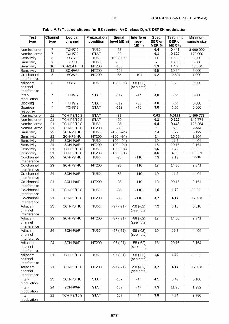
ETSI
ETSI EN 300 394-1 V3.3.1 (2015-04)86
Table A.7: Test conditions for BS receiver V+D, class D, π/8-D8PSK modulation
Test type
Channel type
Logical channel
Propagation condition
Signal level (dBm)
Interferer level
(dBm)
Spec. BER or MER %
Test limit BER or MER %
Minimum sample size
Nominal error 7 TCH/7,2 TU50 -85 0,4 0,448 3 600 000 Nominal error 7 TCH/7,2 STAT -20 0,1 0,122 170 000 Sensitivity 8 SCH/F TU50 -106 (-100) 11 12,32 6 600 Sensitivity 9 STCH TU50 -106 9 10,08 6 600 Sensitivity 10 TCH/2,4 N = 1 HT200 -106 1,3 1,456 45 000 Sensitivity 11 SCH/HU HT200 -106 9,5 10,64 5 000 Co-channel interference
8 SCH/F HT200 -85 -104 9,2 10,304 7 000
Adjacent channel interference
8 SCH/F TU50 -103 (-97) -58 (-62) (see note)
6 6,72 9 000
Inter-modulation
7 TCH/7,2 STAT -112 -47 3,0 3,66 5 800
Blocking 7 TCH/7,2 STAT -112 -25 3,0 3,66 5 800 Spurious response
7 TCH/7,2 STAT -112 -45 3,0 3,66 5 800
Nominal error 21 TCH-P8/10,8 STAT -85 0,01 0,0122 1 499 775 Nominal error 21 TCH-P8/10,8 STAT -20 0,1 0,122 149 774 Nominal error 21 TCH-P8/10,8 TU50 -85 0,4 0,448 125 364 Nominal error 21 TCH-P8/10,8 HT200 -85 5 5,6 9 444 Sensitivity 23 SCH-P8/HU TU50 -100 (-94) 7,4 8,29 6 199 Sensitivity 23 SCH-P8/HU HT200 -100 (-94) 14 15,68 2 964 Sensitivity 24 SCH-P8/F TU50 -100 (-94) 10 11,2 4 404 Sensitivity 24 SCH-P8/F HT200 -100 (-94) 18 20,16 2 164 Sensitivity 21 TCH-P8/10,8 TU50 -100 (-94) 1,6 1,79 30 321 Sensitivity 21 TCH-P8/10,8 HT200 -100 (-94) 3,6 4,03 13 259 Co-channel interference
23 SCH-P8/HU TU50 -85 -110 7,3 8,18 6 318
Co-channel interference
23 SCH-P8/HU HT200 -85 -110 13 14,56 3 241
Co-channel interference
24 SCH-P8/F TU50 -85 -110 10 11,2 4 404
Co-channel interference
24 SCH-P8/F HT200 -85 -110 18 20,16 2 164
Co-channel interference
21 TCH-P8/10,8 TU50 -85 -110 1,6 1,79 30 321
Co-channel interference
21 TCH-P8/10,8 HT200 -85 -110 3,7 4,14 12 788
Adjacent channel interference
23 SCH-P8/HU TU50 -97 (-91) -58 (-62) (see note)
7,3 8,18 6 318
Adjacent channel interference
23 SCH-P8/HU HT200 -97 (-91) -58 (-62) (see note)
13 14,56 3 241
Adjacent channel interference
24 SCH-P8/F TU50 -97 (-91) -58 (-62) (see note)
10 11,2 4 404
Adjacent channel interference
24 SCH-P8/F HT200 -97 (-91) -58 (-62) (see note)
18 20,16 2 164
Adjacent channel interference
21 TCH-P8/10,8 TU50 -97 (-91) -58 (-62) (see note)
1,6 1,79 30 321
Adjacent channel interference
21 TCH-P8/10,8 HT200 -97 (-91) -58 (-62) (see note)
3,7 4,14 12 788
Inter-modulation
23 SCH-P8/HU STAT -107 -47 4,5 5,49 3 108
Inter-modulation
24 SCH-P8/F STAT -107 -47 9,3 11,35 1 392
Inter-modulation
21 TCH-P8/10,8 STAT -107 -47 3,8 4,64 3 750
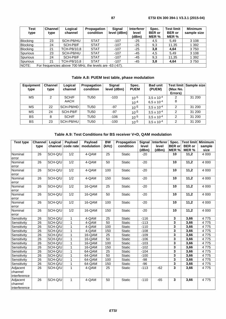
ETSI
ETSI EN 300 394-1 V3.3.1 (2015-04)87
Test type
Channel type
Logical channel
Propagation condition
Signal level (dBm)
Interferer level
(dBm)
Spec. BER or MER %
Test limit BER or MER %
Minimum sample size
Blocking 23 SCH-P8/HU STAT -107 -25 4,5 5,49 3 108 Blocking 24 SCH-P8/F STAT -107 -25 9,3 11,35 1 392 Blocking 21 TCH-P8/10,8 STAT -107 -25 3,8 4,64 3 750 Spurious 23 SCH-P8/HU STAT -107 -45 4,5 5,49 3 108 Spurious 24 SCH-P8/F STAT -107 -45 9,3 11,35 1 392 Spurious 21 TCH-P8/10,8 STAT -107 -45 3,8 4,64 3 750 NOTE: For frequencies above 700 MHz, the levels are -63 (-67).
Table A.8: PUEM test table, phase modulation
Equipment type
Channel type
Logical channel
Propagation condition
Signal level (dBm)
Spec. PUEM
Bad unit (PUEM)
Test limit (Max No. Errors)
Sample size
MS 2 SCH/F AACH
TU50 -103 10-5
10-4
3,5 x 10⁻⁴
6,5 x 10⁻⁴ 2 8
31 200
MS 22 SCH-P8/HD TU50 -97 10-5 3,5 x 10⁻⁴ 2 31 200 MS 24 SCH-P8/F TU50 -97 10-5 3,5 x 10⁻⁴ 2 31 200 BS 8 SCH/F TU50 -106 10-5 3,5 x 10⁻⁴ 2 31 200 BS 23 SCH-P8/HU TU50 -100 10-5 3,5 x 10⁻⁴ 2 31 200
Table A.9: Test Conditions for BS receiver V+D, QAM modulation
Test type Channel type
Logical channel
Payload code rate
Payload modulation
BW (kHz)
Propagation condition
Signal level
(dBm)
Interferer level
(dBm)
Spec. BER or MER %
Test limit BER or MER %
Minimum sample
size Nominal error
26 SCH-Q/U 1/2 4-QAM 25 Static -20 10 11,2 4 000
Nominal error
26 SCH-Q/U 1/2 4-QAM 50 Static -20 10 11,2 4 000
Nominal error
26 SCH-Q/U 1/2 4-QAM 100 Static -20 10 11,2 4 000
Nominal error
26 SCH-Q/U 1/2 4-QAM 150 Static -20 10 11,2 4 000
Nominal error
26 SCH-Q/U 1/2 16-QAM 25 Static -20 10 11,2 4 000
Nominal error
26 SCH-Q/U 1/2 16-QAM 50 Static -20 10 11,2 4 000
Nominal error
26 SCH-Q/U 1/2 16-QAM 100 Static -20 10 11,2 4 000
Nominal error
26 SCH-Q/U 1/2 16-QAM 150 Static -20 10 11,2 4 000
Sensitivity 26 SCH-Q/U 1 4-QAM 25 Static -116 3 3,66 4 775 Sensitivity 26 SCH-Q/U 1 4-QAM 50 Static -113 3 3,66 4 775 Sensitivity 26 SCH-Q/U 1 4-QAM 100 Static -110 3 3,66 4 775 Sensitivity 26 SCH-Q/U 1 4-QAM 150 Static -108 3 3,66 4 775 Sensitivity 26 SCH-Q/U 1 16-QAM 25 Static -109 3 3,66 4 775 Sensitivity 26 SCH-Q/U 1 16-QAM 50 Static -106 3 3,66 4 775 Sensitivity 26 SCH-Q/U 1 16-QAM 100 Static -103 3 3,66 4 775 Sensitivity 26 SCH-Q/U 1 16-QAM 150 Static -102 3 3,66 4 775 Sensitivity 26 SCH-Q/U 1 64-QAM 25 Static -104 3 3,66 4 775 Sensitivity 26 SCH-Q/U 1 64-QAM 50 Static -100 3 3,66 4 775 Sensitivity 26 SCH-Q/U 1 64-QAM 100 Static -98 3 3,66 4 775 Sensitivity 26 SCH-Q/U 1 64-QAM 150 Static -96 3 3,66 4 775 Adjacent channel interference
26 SCH-Q/U 1 4-QAM 25 Static -113 -62 3 3,66 4 775
Adjacent channel interference
26 SCH-Q/U 1 4-QAM 50 Static -110 -65 3 3,66 4 775

ETSI
ETSI EN 300 394-1 V3.3.1 (2015-04)88
Test type Channel type
Logical channel
Payload code rate
Payload modulation
BW (kHz)
Propagation condition
Signal level
(dBm)
Interferer level
(dBm)
Spec. BER or MER %
Test limit BER or MER %
Minimum sample
size Adjacent channel interference
26 SCH-Q/U 1 4-QAM 100 Static -107 -65 3 3,66 4 775
Adjacent channel interference
26 SCH-Q/U 1 4-QAM 150 Static -105 -65 3 3,66 4 775
Adjacent channel interference
26 SCH-Q/U 1 16-QAM 25 Static -106 (-100)
-62 (-66)
3 3,66 4 775
Adjacent channel interference
26 SCH-Q/U 1 16-QAM 50 Static -103 (-97)
-65 (-69)
3 3,66 4 775
Adjacent channel interference
26 SCH-Q/U 1 16-QAM 100 Static -100 (-94)
-65 (-69)
3 3,66 4 775
Adjacent channel interference
26 SCH-Q/U 1 16-QAM 150 Static -99 (-93)
-65 (-69)
3 3,66 4 775
Adjacent channel interference
26 SCH-Q/U 1 64-QAM 25 Static -101 -62 3 3,66 4 775
Adjacent channel interference
26 SCH-Q/U 1 64-QAM 50 Static -97 -65 3 3,66 4 775
Adjacent channel interference
26 SCH-Q/U 1 64-QAM 100 Static -95 -65 3 3,66 4 775
Adjacent channel interference
26 SCH-Q/U 1 64-QAM 150 Static -93 -65 3 3,66 4 775
Blocking 26 SCH-Q/U 1 4-QAM 25 Static -113 -40 3 3,66 4 775 Blocking 26 SCH-Q/U 1 4-QAM 25 Static -113 -35 3 3,66 4 775 Blocking 26 SCH-Q/U 1 4-QAM 25 Static -113 -30 3 3,66 4 775 Blocking 26 SCH-Q/U 1 4-QAM 25 Static -113 -25 3 3,66 4 775 Blocking 26 SCH-Q/U 1 4-QAM 50 Static -110 -40 3 3,66 4 775 Blocking 26 SCH-Q/U 1 4-QAM 50 Static -110 -35 3 3,66 4 775 Blocking 26 SCH-Q/U 1 4-QAM 50 Static -110 -30 3 3,66 4 775 Blocking 26 SCH-Q/U 1 4-QAM 50 Static -110 -25 3 3,66 4 775 Blocking 26 SCH-Q/U 1 4-QAM 100 Static -107 -40 3 3,66 4 775 Blocking 26 SCH-Q/U 1 4-QAM 100 Static -107 -35 3 3,66 4 775 Blocking 26 SCH-Q/U 1 4-QAM 100 Static -107 -30 3 3,66 4 775 Blocking 26 SCH-Q/U 1 4-QAM 100 Static -107 -25 3 3,66 4 775 Blocking 26 SCH-Q/U 1 4-QAM 150 Static -105 -40 3 3,66 4 775 Blocking 26 SCH-Q/U 1 4-QAM 150 Static -105 -35 3 3,66 4 775 Blocking 26 SCH-Q/U 1 4-QAM 150 Static -105 -30 3 3,66 4 775 Blocking 26 SCH-Q/U 1 4-QAM 150 Static -105 -25 3 3,66 4 775 Blocking 26 SCH-Q/U 1 16-QAM 25 Static -106 -40 3 3,66 4 775 Blocking 26 SCH-Q/U 1 16-QAM 25 Static -106 -35 3 3,66 4 775 Blocking 26 SCH-Q/U 1 16-QAM 25 Static -106 -30 3 3,66 4 775 Blocking 26 SCH-Q/U 1 16-QAM 25 Static -106 -25 3 3,66 4 775 Blocking 26 SCH-Q/U 1 16-QAM 50 Static -103 -40 3 3,66 4 775 Blocking 26 SCH-Q/U 1 16-QAM 50 Static -103 -35 3 3,66 4 775 Blocking 26 SCH-Q/U 1 16-QAM 50 Static -103 -30 3 3,66 4 775 Blocking 26 SCH-Q/U 1 16-QAM 50 Static -103 -25 3 3,66 4 775 Blocking 26 SCH-Q/U 1 16-QAM 100 Static -100 -40 3 3,66 4 775 Blocking 26 SCH-Q/U 1 16-QAM 100 Static -100 -35 3 3,66 4 775 Blocking 26 SCH-Q/U 1 16-QAM 100 Static -100 -30 3 3,66 4 775 Blocking 26 SCH-Q/U 1 16-QAM 100 Static -100 -25 3 3,66 4 775 Blocking 26 SCH-Q/U 1 16-QAM 150 Static -99 -40 3 3,66 4 775 Blocking 26 SCH-Q/U 1 16-QAM 150 Static -99 -35 3 3,66 4 775 Blocking 26 SCH-Q/U 1 16-QAM 150 Static -99 -30 3 3,66 4 775 Blocking 26 SCH-Q/U 1 16-QAM 150 Static -99 -25 3 3,66 4 775 Blocking 26 SCH-Q/U 1 64-QAM 25 Static -101 -40 3 3,66 4 775
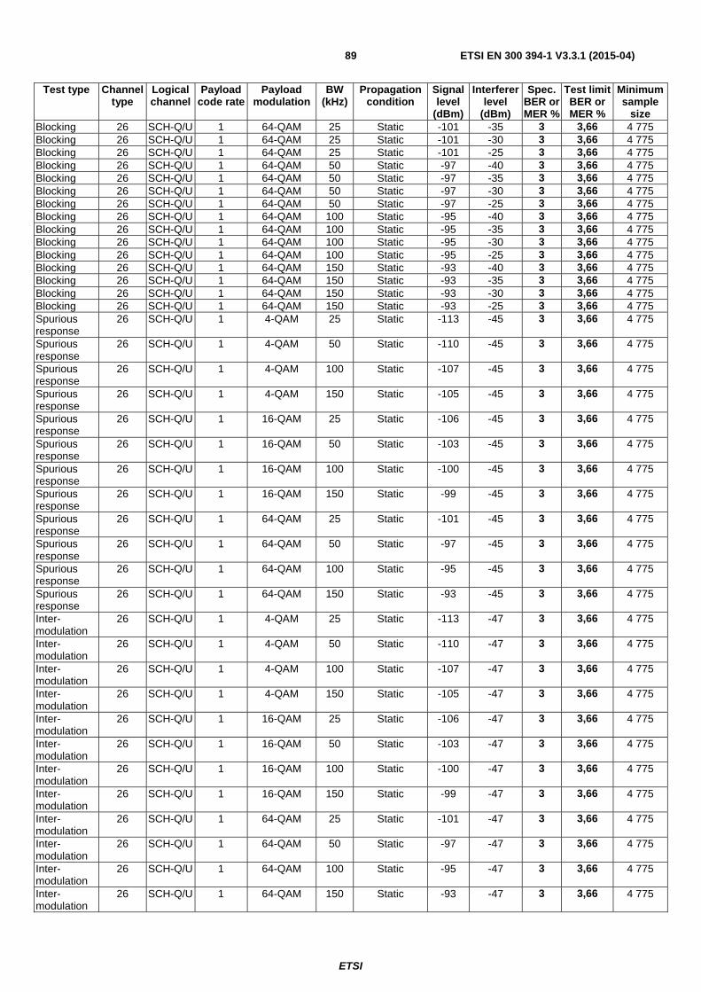
ETSI
ETSI EN 300 394-1 V3.3.1 (2015-04)89
Test type Channel type
Logical channel
Payload code rate
Payload modulation
BW (kHz)
Propagation condition
Signal level
(dBm)
Interferer level
(dBm)
Spec. BER or MER %
Test limit BER or MER %
Minimum sample
size Blocking 26 SCH-Q/U 1 64-QAM 25 Static -101 -35 3 3,66 4 775 Blocking 26 SCH-Q/U 1 64-QAM 25 Static -101 -30 3 3,66 4 775 Blocking 26 SCH-Q/U 1 64-QAM 25 Static -101 -25 3 3,66 4 775 Blocking 26 SCH-Q/U 1 64-QAM 50 Static -97 -40 3 3,66 4 775 Blocking 26 SCH-Q/U 1 64-QAM 50 Static -97 -35 3 3,66 4 775 Blocking 26 SCH-Q/U 1 64-QAM 50 Static -97 -30 3 3,66 4 775 Blocking 26 SCH-Q/U 1 64-QAM 50 Static -97 -25 3 3,66 4 775 Blocking 26 SCH-Q/U 1 64-QAM 100 Static -95 -40 3 3,66 4 775 Blocking 26 SCH-Q/U 1 64-QAM 100 Static -95 -35 3 3,66 4 775 Blocking 26 SCH-Q/U 1 64-QAM 100 Static -95 -30 3 3,66 4 775 Blocking 26 SCH-Q/U 1 64-QAM 100 Static -95 -25 3 3,66 4 775 Blocking 26 SCH-Q/U 1 64-QAM 150 Static -93 -40 3 3,66 4 775 Blocking 26 SCH-Q/U 1 64-QAM 150 Static -93 -35 3 3,66 4 775 Blocking 26 SCH-Q/U 1 64-QAM 150 Static -93 -30 3 3,66 4 775 Blocking 26 SCH-Q/U 1 64-QAM 150 Static -93 -25 3 3,66 4 775 Spurious response
26 SCH-Q/U 1 4-QAM 25 Static -113 -45 3 3,66 4 775
Spurious response
26 SCH-Q/U 1 4-QAM 50 Static -110 -45 3 3,66 4 775
Spurious response
26 SCH-Q/U 1 4-QAM 100 Static -107 -45 3 3,66 4 775
Spurious response
26 SCH-Q/U 1 4-QAM 150 Static -105 -45 3 3,66 4 775
Spurious response
26 SCH-Q/U 1 16-QAM 25 Static -106 -45 3 3,66 4 775
Spurious response
26 SCH-Q/U 1 16-QAM 50 Static -103 -45 3 3,66 4 775
Spurious response
26 SCH-Q/U 1 16-QAM 100 Static -100 -45 3 3,66 4 775
Spurious response
26 SCH-Q/U 1 16-QAM 150 Static -99 -45 3 3,66 4 775
Spurious response
26 SCH-Q/U 1 64-QAM 25 Static -101 -45 3 3,66 4 775
Spurious response
26 SCH-Q/U 1 64-QAM 50 Static -97 -45 3 3,66 4 775
Spurious response
26 SCH-Q/U 1 64-QAM 100 Static -95 -45 3 3,66 4 775
Spurious response
26 SCH-Q/U 1 64-QAM 150 Static -93 -45 3 3,66 4 775
Inter-modulation
26 SCH-Q/U 1 4-QAM 25 Static -113 -47 3 3,66 4 775
Inter-modulation
26 SCH-Q/U 1 4-QAM 50 Static -110 -47 3 3,66 4 775
Inter-modulation
26 SCH-Q/U 1 4-QAM 100 Static -107 -47 3 3,66 4 775
Inter-modulation
26 SCH-Q/U 1 4-QAM 150 Static -105 -47 3 3,66 4 775
Inter-modulation
26 SCH-Q/U 1 16-QAM 25 Static -106 -47 3 3,66 4 775
Inter-modulation
26 SCH-Q/U 1 16-QAM 50 Static -103 -47 3 3,66 4 775
Inter-modulation
26 SCH-Q/U 1 16-QAM 100 Static -100 -47 3 3,66 4 775
Inter-modulation
26 SCH-Q/U 1 16-QAM 150 Static -99 -47 3 3,66 4 775
Inter-modulation
26 SCH-Q/U 1 64-QAM 25 Static -101 -47 3 3,66 4 775
Inter-modulation
26 SCH-Q/U 1 64-QAM 50 Static -97 -47 3 3,66 4 775
Inter-modulation
26 SCH-Q/U 1 64-QAM 100 Static -95 -47 3 3,66 4 775
Inter-modulation
26 SCH-Q/U 1 64-QAM 150 Static -93 -47 3 3,66 4 775
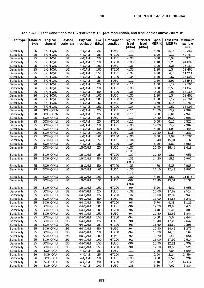
ETSI
ETSI EN 300 394-1 V3.3.1 (2015-04)90
Table A.10: Test Conditions for BS receiver V+D, QAM modulation, and frequencies above 700 MHz
Test type Channel type
Logical channel
Payload code rate
Payload modulation
BW (kHz)
Propagation condition
Signal level
(dBm)
Interferer level
(dBm)
Spec. MER %
Test limit MER %
Minimum sample
size Sensitivity 25 SICH-Q/U 1/2 4-QAM 25 TU50 -111 4,60 5,15 10 257 Sensitivity 25 SICH-Q/U 1/2 4-QAM 25 HT200 -111 1,00 1,12 49 764 Sensitivity 25 SICH-Q/U 1/2 4-QAM 50 TU50 -108 5,30 5,94 8 970 Sensitivity 25 SICH-Q/U 1/2 4-QAM 50 HT200 -108 1,10 1,23 44 032 Sensitivity 25 SICH-Q/U 1/2 4-QAM 100 TU50 -105 3,00 3,36 16 164 Sensitivity 25 SICH-Q/U 1/2 4-QAM 100 HT200 -105 1,20 1,34 39 463 Sensitivity 25 SICH-Q/U 1/2 4-QAM 150 TU50 -104 4,20 4,7 11 211 Sensitivity 25 SICH-Q/U 1/2 4-QAM 150 HT200 -104 1,40 1,57 36 097 Sensitivity 26 SICH-Q/U 1/2 4-QAM 25 TU50 -111 2,60 2,91 18 545 Sensitivity 26 SICH-Q/U 1/2 4-QAM 25 HT200 -111 1,00 1,12 49 764 Sensitivity 26 SICH-Q/U 1/2 4-QAM 50 TU50 -108 3,20 3,58 14 848 Sensitivity 26 SICH-Q/U 1/2 4-QAM 50 HT200 -108 0,90 1,01 57 165 Sensitivity 26 SICH-Q/U 1/2 4-QAM 100 TU50 -105 1,20 1,34 39 463 Sensitivity 26 SICH-Q/U 1/2 4-QAM 100 HT200 -105 1,00 1,12 49 764 Sensitivity 26 SICH-Q/U 1/2 4-QAM 150 TU50 -104 3,70 4,14 12 788 Sensitivity 26 SICH-Q/U 1/2 4-QAM 150 HT200 -104 1,40 1,57 36 097 Sensitivity 28 SCH-Q/RA 1/2 4-QAM 25 TU50 -111 14,20 15,9 2 902 Sensitivity 28 SCH-Q/RA 1/2 4-QAM 25 HT200 -111 5,90 6,61 7 945 Sensitivity 25 SCH-Q/HU 1/2 4-QAM 25 TU50 -111 14,30 16,02 2 901 Sensitivity 25 SCH-Q/HU 1/2 4-QAM 25 HT200 -111 5,50 6,16 8 528 Sensitivity 25 SCH-Q/HU 1/2 4-QAM 50 TU50 -108 14,20 15,9 2 902 Sensitivity 25 SCH-Q/HU 1/2 4-QAM 50 HT200 -108 4,40 4,93 10 890 Sensitivity 25 SCH-Q/HU 1/2 4-QAM 100 TU50 -105 10,30 11,54 4 281 Sensitivity 25 SCH-Q/HU 1/2 4-QAM 100 HT200 -105 3,50 3,92 13 764 Sensitivity 25 SCH-Q/HU 1/2 4-QAM 150 TU50 -104 13,40 15,01 3 132 Sensitivity 25 SCH-Q/HU 1/2 4-QAM 150 HT200 -104 5,20 5,82 8 958 Sensitivity 25 SCH-Q/HU 1/2 16-QAM 25 TU50 -107
(-101) 16,50 18,48 2 419
Sensitivity 25 SCH-Q/HU 1/2 16-QAM 25 HT200 -107 10,80 12,1 4 053 Sensitivity 25 SCH-Q/HU 1/2 16-QAM 50 TU50 -103
(-97) 14,20 15,9 2 902
Sensitivity 25 SCH-Q/HU 1/2 16-QAM 50 HT200 -103 4,80 5,38 9 983 Sensitivity 25 SCH-Q/HU 1/2 16-QAM 100 TU50 -100
(- 94) 11,10 12,43 3 895
Sensitivity 25 SCH-Q/HU 1/2 16-QAM 100 HT200 -100 4,10 4,59 11 576 Sensitivity 25 SCH-Q/HU 1/2 16-QAM 150 TU50 -99
(-93) 13,40 15,01 3 132
Sensitivity 25 SCH-Q/HU 1/2 16-QAM 150 HT200 -99 5,20 5,82 8 958 Sensitivity 25 SCH-Q/HU 1/2 64-QAM 25 TU50 -102 16,00 17,92 2 514 Sensitivity 25 SCH-Q/HU 1/2 64-QAM 25 HT200 -102 11,00 12,32 3 946 Sensitivity 25 SCH-Q/HU 1/2 64-QAM 50 TU50 -98 13,00 14,56 3 241 Sensitivity 25 SCH-Q/HU 1/2 64-QAM 50 HT200 -98 5,70 6,38 8 125 Sensitivity 25 SCH-Q/HU 1/2 64-QAM 100 TU50 -96 12,20 13,66 3 479 Sensitivity 25 SCH-Q/HU 1/2 64-QAM 100 HT200 -96 8,40 9,41 5 383 Sensitivity 25 SCH-Q/HU 1/2 64-QAM 150 TU50 -94 11,30 12,66 3 844 Sensitivity 25 SCH-Q/HU 1/2 64-QAM 150 HT200 -94 5,00 5,6 9 444 Sensitivity 25 SCH-Q/HU 2/3 64-QAM 25 TU50 -98 15,40 17,25 2 642 Sensitivity 25 SCH-Q/HU 2/3 64-QAM 25 HT200 -98 16,60 18,59 2 396 Sensitivity 25 SCH-Q/HU 2/3 64-QAM 50 TU50 -94 12,90 14,45 3 279 Sensitivity 25 SCH-Q/HU 2/3 64-QAM 50 HT200 -94 13,20 14,78 3 169 Sensitivity 25 SCH-Q/HU 2/3 64-QAM 100 TU50 -92 11,70 13,1 3 654 Sensitivity 25 SCH-Q/HU 2/3 64-QAM 100 HT200 -92 16,00 17,92 2 514 Sensitivity 25 SCH-Q/HU 2/3 64-QAM 150 TU50 -90 10,90 12,21 3 999 Sensitivity 25 SCH-Q/HU 2/3 64-QAM 150 HT200 -90 12,10 13,55 3 521 Sensitivity 26 SCH-Q/U 1/2 4-QAM 25 TU50 -111 7,00 7,84 6 564 Sensitivity 26 SCH-Q/U 1/2 4-QAM 25 HT200 -111 2,00 2,24 24 564 Sensitivity 26 SCH-Q/U 1/2 4-QAM 50 TU50 -108 8,50 9,52 5 294 Sensitivity 26 SCH-Q/U 1/2 4-QAM 50 HT200 -108 1,10 1,23 44 032 Sensitivity 26 SCH-Q/U 1/2 4-QAM 100 TU50 -105 6,80 7,62 6 834
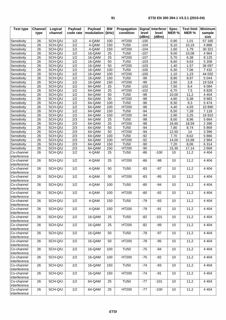
ETSI
ETSI EN 300 394-1 V3.3.1 (2015-04)91
Test type Channel type
Logical channel
Payload code rate
Payload modulation
BW (kHz)
Propagation condition
Signal level
(dBm)
Interferer level
(dBm)
Spec. MER %
Test limit MER %
Minimum sample
size Sensitivity 26 SCH-Q/U 1/2 4-QAM 100 HT200 -105 0,90 1,01 57 165 Sensitivity 26 SCH-Q/U 1/2 4-QAM 150 TU50 -104 9,10 10,19 4 888 Sensitivity 26 SCH-Q/U 1/2 4-QAM 150 HT200 -104 1,60 1,79 30 321 Sensitivity 26 SCH-Q/U 1/2 16-QAM 25 TU50 -107 9,00 10,08 4 964 Sensitivity 26 SCH-Q/U 1/2 16-QAM 25 HT200 -107 5,70 6,38 8 125 Sensitivity 26 SCH-Q/U 1/2 16-QAM 50 TU50 -103 8,60 9,63 5 208 Sensitivity 26 SCH-Q/U 1/2 16-QAM 50 HT200 -103 1,40 1,57 36 097 Sensitivity 26 SCH-Q/U 1/2 16-QAM 100 TU50 -100 6,30 7,06 7 432 Sensitivity 26 SCH-Q/U 1/2 16-QAM 100 HT200 -100 1,10 1,23 44 032 Sensitivity 26 SCH-Q/U 1/2 16-QAM 150 TU50 -99 8,90 9,97 5 044 Sensitivity 26 SCH-Q/U 1/2 16-QAM 150 HT200 -99 2,50 2,8 19 524 Sensitivity 26 SCH-Q/U 1/2 64-QAM 25 TU50 -102 7,50 8,4 6 084 Sensitivity 26 SCH-Q/U 1/2 64-QAM 25 HT200 -102 6,70 7,5 6 828 Sensitivity 26 SCH-Q/U 1/2 64-QAM 50 TU50 -98 10,00 11,2 4 404 Sensitivity 26 SCH-Q/U 1/2 64-QAM 50 HT200 -98 4,80 5,38 9 983 Sensitivity 26 SCH-Q/U 1/2 64-QAM 100 TU50 -96 8,30 9,3 5 474 Sensitivity 26 SCH-Q/U 1/2 64-QAM 100 HT200 -96 4,40 4,93 10 890 Sensitivity 26 SCH-Q/U 1/2 64-QAM 150 TU50 -94 6,50 7,28 7 118 Sensitivity 26 SCH-Q/U 1/2 64-QAM 150 HT200 -94 2,90 3,25 16 910 Sensitivity 26 SCH-Q/U 2/3 64-QAM 25 TU50 -98 8,00 8,96 5 664 Sensitivity 26 SCH-Q/U 2/3 64-QAM 25 HT200 -98 16,60 18,59 2 396 Sensitivity 26 SCH-Q/U 2/3 64-QAM 50 TU50 -94 7,80 8,74 5 869 Sensitivity 26 SCH-Q/U 2/3 64-QAM 50 HT200 -94 12,50 14 3 396 Sensitivity 26 SCH-Q/U 2/3 64-QAM 100 TU50 -92 7,70 8,62 5 866 Sensitivity 26 SCH-Q/U 2/3 64-QAM 100 HT200 -92 14,00 15,68 2 964 Sensitivity 26 SCH-Q/U 2/3 64-QAM 150 TU50 -90 7,20 8,06 6 314 Sensitivity 26 SCH-Q/U 2/3 64-QAM 150 HT200 -90 15,30 17,14 2 669 Co-channel interference
26 SCH-Q/U 1/2 4-QAM 25 TU50 -86 -100 10 11,2 4 404
Co-channel interference
26 SCH-Q/U 1/2 4-QAM 25 HT200 -86 -98 10 11,2 4 404
Co-channel interference
26 SCH-Q/U 1/2 4-QAM 50 TU50 -83 -97 10 11,2 4 404
Co-channel interference
26 SCH-Q/U 1/2 4-QAM 50 HT200 -83 -95 10 11,2 4 404
Co-channel interference
26 SCH-Q/U 1/2 4-QAM 100 TU50 -80 -94 10 11,2 4 404
Co-channel interference
26 SCH-Q/U 1/2 4-QAM 100 HT200 -80 -92 10 11,2 4 404
Co-channel interference
26 SCH-Q/U 1/2 4-QAM 150 TU50 -79 -93 10 11,2 4 404
Co-channel interference
26 SCH-Q/U 1/2 4-QAM 150 HT200 -79 -91 10 11,2 4 404
Co-channel interference
26 SCH-Q/U 1/2 16-QAM 25 TU50 -82 -101 10 11,2 4 404
Co-channel interference
26 SCH-Q/U 1/2 16-QAM 25 HT200 -82 -99 10 11,2 4 404
Co-channel interference
26 SCH-Q/U 1/2 16-QAM 50 TU50 -78 -97 10 11,2 4 404
Co-channel interference
26 SCH-Q/U 1/2 16-QAM 50 HT200 -78 -95 10 11,2 4 404
Co-channel interference
26 SCH-Q/U 1/2 16-QAM 100 TU50 -75 -94 10 11,2 4 404
Co-channel interference
26 SCH-Q/U 1/2 16-QAM 100 HT200 -75 -92 10 11,2 4 404
Co-channel interference
26 SCH-Q/U 1/2 16-QAM 150 TU50 -74 -93 10 11,2 4 404
Co-channel interference
26 SCH-Q/U 1/2 16-QAM 150 HT200 -74 -91 10 11,2 4 404
Co-channel interference
26 SCH-Q/U 1/2 64-QAM 25 TU50 -77 -101 10 11,2 4 404
Co-channel interference
26 SCH-Q/U 1/2 64-QAM 25 HT200 -77 -100 10 11,2 4 404
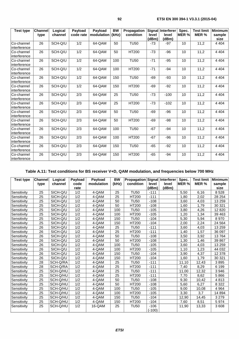
ETSI
ETSI EN 300 394-1 V3.3.1 (2015-04)92
Test type Channel type
Logical channel
Payload code rate
Payload modulation
BW (kHz)
Propagation condition
Signal level
(dBm)
Interferer level
(dBm)
Spec. MER %
Test limit MER %
Minimum sample
size Co-channel interference
26 SCH-Q/U 1/2 64-QAM 50 TU50 -73 -97 10 11,2 4 404
Co-channel interference
26 SCH-Q/U 1/2 64-QAM 50 HT200 -73 -96 10 11,2 4 404
Co-channel interference
26 SCH-Q/U 1/2 64-QAM 100 TU50 -71 -95 10 11,2 4 404
Co-channel interference
26 SCH-Q/U 1/2 64-QAM 100 HT200 -71 -94 10 11,2 4 404
Co-channel interference
26 SCH-Q/U 1/2 64-QAM 150 TU50 -69 -93 10 11,2 4 404
Co-channel interference
26 SCH-Q/U 1/2 64-QAM 150 HT200 -69 -92 10 11,2 4 404
Co-channel interference
26 SCH-Q/U 2/3 64-QAM 25 TU50 -73 -100 10 11,2 4 404
Co-channel interference
26 SCH-Q/U 2/3 64-QAM 25 HT200 -73 -102 10 11,2 4 404
Co-channel interference
26 SCH-Q/U 2/3 64-QAM 50 TU50 -69 -96 10 11,2 4 404
Co-channel interference
26 SCH-Q/U 2/3 64-QAM 50 HT200 -69 -98 10 11,2 4 404
Co-channel interference
26 SCH-Q/U 2/3 64-QAM 100 TU50 -67 -94 10 11,2 4 404
Co-channel interference
26 SCH-Q/U 2/3 64-QAM 100 HT200 -67 -96 10 11,2 4 404
Co-channel interference
26 SCH-Q/U 2/3 64-QAM 150 TU50 -65 -92 10 11,2 4 404
Co-channel interference
26 SCH-Q/U 2/3 64-QAM 150 HT200 -65 -94 10 11,2 4 404
Table A.11: Test conditions for BS receiver V+D, QAM modulation, and frequencies below 700 MHz
Test type Channel type
Logical channel
Payload code rate
Payload modulation
BW (kHz)
Propagation condition
Signal level
(dBm)
Interferer level
(dBm)
Spec. MER %
Test limit MER %
Minimum sample
size Sensitivity 25 SICH-Q/U 1/2 4-QAM 25 TU50 -111 5,50 6,16 8 528 Sensitivity 25 SICH-Q/U 1/2 4-QAM 25 HT200 -111 1,80 2,02 28 254 Sensitivity 25 SICH-Q/U 1/2 4-QAM 50 TU50 -108 3,60 4,03 13 259 Sensitivity 25 SICH-Q/U 1/2 4-QAM 50 HT200 -108 1,60 1,79 30 321 Sensitivity 25 SICH-Q/U 1/2 4-QAM 100 TU50 -105 3,80 4,26 12 820 Sensitivity 25 SICH-Q/U 1/2 4-QAM 100 HT200 -105 1,20 1,34 39 463 Sensitivity 25 SICH-Q/U 1/2 4-QAM 150 TU50 -104 5,30 5,94 8 970 Sensitivity 25 SICH-Q/U 1/2 4-QAM 150 HT200 -104 2,00 2,24 24 564 Sensitivity 26 SICH-Q/U 1/2 4-QAM 25 TU50 -111 3,60 4,03 13 259 Sensitivity 26 SICH-Q/U 1/2 4-QAM 25 HT200 -111 1,40 1,57 36 097 Sensitivity 26 SICH-Q/U 1/2 4-QAM 50 TU50 -108 3,50 3,92 13 764 Sensitivity 26 SICH-Q/U 1/2 4-QAM 50 HT200 -108 1,30 1,46 39 867 Sensitivity 26 SICH-Q/U 1/2 4-QAM 100 TU50 -105 3,60 4,03 13 259 Sensitivity 26 SICH-Q/U 1/2 4-QAM 100 HT200 -105 1,10 1,23 44 032 Sensitivity 26 SICH-Q/U 1/2 4-QAM 150 TU50 -104 3,90 4,37 12 378 Sensitivity 26 SICH-Q/U 1/2 4-QAM 150 HT200 -104 1,60 1,79 30 321 Sensitivity 28 SCH-Q/RA 1/2 4-QAM 25 TU50 -111 11,10 12,43 3 895 Sensitivity 28 SCH-Q/RA 1/2 4-QAM 25 HT200 -111 7,40 8,29 6 199 Sensitivity 25 SCH-Q/HU 1/2 4-QAM 25 TU50 -111 11,00 12,32 3 946 Sensitivity 25 SCH-Q/HU 1/2 4-QAM 25 HT200 -111 7,70 8,62 5 866 Sensitivity 25 SCH-Q/HU 1/2 4-QAM 50 TU50 -108 9,30 10,42 4 813 Sensitivity 25 SCH-Q/HU 1/2 4-QAM 50 HT200 -108 5,60 6,27 8 322 Sensitivity 25 SCH-Q/HU 1/2 4-QAM 100 TU50 -105 9,00 10,08 4 964 Sensitivity 25 SCH-Q/HU 1/2 4-QAM 100 HT200 -105 3,30 3,7 14 894 Sensitivity 25 SCH-Q/HU 1/2 4-QAM 150 TU50 -104 12,90 14,45 3 279 Sensitivity 25 SCH-Q/HU 1/2 4-QAM 150 HT200 -104 7,60 8,51 5 974 Sensitivity 25 SCH-Q/HU 1/2 16-QAM 25 TU50 -106
(-100) 11,90 13,33 3 608

ETSI
ETSI EN 300 394-1 V3.3.1 (2015-04)93
Test type Channel type
Logical channel
Payload code rate
Payload modulation
BW (kHz)
Propagation condition
Signal level
(dBm)
Interferer level
(dBm)
Spec. MER %
Test limit MER %
Minimum sample
size Sensitivity 25 SCH-Q/HU 1/2 16-QAM 25 HT200 -106 8,20 9,18 5 473 Sensitivity 25 SCH-Q/HU 1/2 16-QAM 50 TU50 -102
(-96) 7,90 8,85 5 765
Sensitivity 25 SCH-Q/HU 1/2 16-QAM 50 HT200 -102 3,60 4,03 13 259 Sensitivity 25 SCH-Q/HU 1/2 16-QAM 100 TU50 -100
(-94) 9,90 11,09 4 468
Sensitivity 25 SCH-Q/HU 1/2 16-QAM 100 HT200 -100 3,50 3,92 13 764 Sensitivity 25 SCH-Q/HU 1/2 16-QAM 150 TU50 -99
(-93) 13,20 14,78 3 169
Sensitivity 25 SCH-Q/HU 1/2 16-QAM 150 HT200 -99 7,50 8,4 6 084 Sensitivity 25 SCH-Q/HU 1/2 64-QAM 25 TU50 -101 11,00 12,32 3 946 Sensitivity 25 SCH-Q/HU 1/2 64-QAM 25 HT200 -101 7,00 7,84 6 564 Sensitivity 25 SCH-Q/HU 1/2 64-QAM 50 TU50 -98 8,90 9,97 5 044 Sensitivity 25 SCH-Q/HU 1/2 64-QAM 50 HT200 -98 4,80 5,38 9 983 Sensitivity 25 SCH-Q/HU 1/2 64-QAM 100 TU50 -95 8,70 9,74 5 124 Sensitivity 25 SCH-Q/HU 1/2 64-QAM 100 HT200 -95 3,00 3,36 16 164 Sensitivity 25 SCH-Q/HU 1/2 64-QAM 150 TU50 -94 12,10 13,55 3 521 Sensitivity 25 SCH-Q/HU 1/2 64-QAM 150 HT200 -94 6,20 6,94 7 425 Sensitivity 25 SCH-Q/HU 2/3 64-QAM 25 TU50 -98 11,20 12,54 3 845 Sensitivity 25 SCH-Q/HU 2/3 64-QAM 25 HT200 -98 11,20 12,54 3 845 Sensitivity 25 SCH-Q/HU 2/3 64-QAM 50 TU50 -94 7,80 8,74 5 869 Sensitivity 25 SCH-Q/HU 2/3 64-QAM 50 HT200 -94 7,60 8,51 5 974 Sensitivity 25 SCH-Q/HU 2/3 64-QAM 100 TU50 -92 9,90 11,09 4 468 Sensitivity 25 SCH-Q/HU 2/3 64-QAM 100 HT200 -92 7,10 7,95 6 437 Sensitivity 25 SCH-Q/HU 2/3 64-QAM 150 TU50 -91 14,10 15,79 2 933 Sensitivity 25 SCH-Q/HU 2/3 64-QAM 150 HT200 -91 11,80 13,22 3 653 Sensitivity 26 SCH-Q/U 1/2 4-QAM 25 TU50 -111 8,30 9,3 5 474 Sensitivity 26 SCH-Q/U 1/2 4-QAM 25 HT200 -111 3,70 4,14 12 788 Sensitivity 26 SCH-Q/U 1/2 4-QAM 50 TU50 -108 9,40 10,53 4 741 Sensitivity 26 SCH-Q/U 1/2 4-QAM 50 HT200 -108 2,00 2,24 24 564 Sensitivity 26 SCH-Q/U 1/2 4-QAM 100 TU50 -105 9,00 10,08 4 964 Sensitivity 26 SCH-Q/U 1/2 4-QAM 100 HT200 -105 1,50 1,68 32 964 Sensitivity 26 SCH-Q/U 1/2 4-QAM 150 TU50 -104 8,10 9,07 5 567 Sensitivity 26 SCH-Q/U 1/2 4-QAM 150 HT200 -104 3,20 3,58 14 848 Sensitivity 26 SCH-Q/U 1/2 16-QAM 25 TU50 -106 8,80 9,86 5 125 Sensitivity 26 SCH-Q/U 1/2 16-QAM 25 HT200 -106 3,90 4,37 12 378 Sensitivity 26 SCH-Q/U 1/2 16-QAM 50 TU50 -102 7,00 7,84 6 564 Sensitivity 26 SCH-Q/U 1/2 16-QAM 50 HT200 -102 1,10 1,23 44 032 Sensitivity 26 SCH-Q/U 1/2 16-QAM 100 TU50 -100 9,50 10,64 4 670 Sensitivity 26 SCH-Q/U 1/2 16-QAM 100 HT200 -100 1,60 1,79 30 321 Sensitivity 26 SCH-Q/U 1/2 16-QAM 150 TU50 -99 8,90 9,97 5 044 Sensitivity 26 SCH-Q/U 1/2 16-QAM 150 HT200 -99 3,50 3,92 13 764 Sensitivity 26 SCH-Q/U 1/2 64-QAM 25 TU50 -101 7,80 8,74 5 869 Sensitivity 26 SCH-Q/U 1/2 64-QAM 25 HT200 -101 3,70 4,14 12 788 Sensitivity 26 SCH-Q/U 1/2 64-QAM 50 TU50 -98 9,90 11,09 4 468 Sensitivity 26 SCH-Q/U 1/2 64-QAM 50 HT200 -98 3,00 3,36 16 164 Sensitivity 26 SCH-Q/U 1/2 64-QAM 100 TU50 -95 7,70 8,62 5 866 Sensitivity 26 SCH-Q/U 1/2 64-QAM 100 HT200 -95 1,60 1,79 30 321 Sensitivity 26 SCH-Q/U 1/2 64-QAM 150 TU50 -94 6,90 7,73 6 697 Sensitivity 26 SCH-Q/U 1/2 64-QAM 150 HT200 -94 2,70 3,02 17 655 Sensitivity 26 SCH-Q/U 2/3 64-QAM 25 TU50 -98 9,50 10,64 4 670 Sensitivity 26 SCH-Q/U 2/3 64-QAM 25 HT200 -98 7,70 8,62 5 866 Sensitivity 26 SCH-Q/U 2/3 64-QAM 50 TU50 -94 8,30 9,3 5 474 Sensitivity 26 SCH-Q/U 2/3 64-QAM 50 HT200 -94 4,40 4,93 10 890 Sensitivity 26 SCH-Q/U 2/3 64-QAM 100 TU50 -92 9,60 10,75 4 601 Sensitivity 26 SCH-Q/U 2/3 64-QAM 100 HT200 -92 5,10 5,71 9 195 Sensitivity 26 SCH-Q/U 2/3 64-QAM 150 TU50 -91 9,30 10,42 4 813 Sensitivity 26 SCH-Q/U 2/3 64-QAM 150 HT200 -91 8,10 9,07 5 567 Co-channel interference
26 SCH-Q/U 1/2 4-QAM 25 TU50 -86 -100 10 11,2 4 404
Co-channel interference
26 SCH-Q/U 1/2 4-QAM 25 HT200 -86 -98 10 11,2 4 404
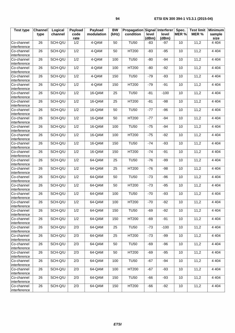
ETSI
ETSI EN 300 394-1 V3.3.1 (2015-04)94
Test type Channel type
Logical channel
Payload code rate
Payload modulation
BW (kHz)
Propagation condition
Signal level
(dBm)
Interferer level
(dBm)
Spec. MER %
Test limit MER %
Minimum sample
size Co-channel interference
26 SCH-Q/U 1/2 4-QAM 50 TU50 -83 -97 10 11,2 4 404
Co-channel interference
26 SCH-Q/U 1/2 4-QAM 50 HT200 -83 -95 10 11,2 4 404
Co-channel interference
26 SCH-Q/U 1/2 4-QAM 100 TU50 -80 -94 10 11,2 4 404
Co-channel interference
26 SCH-Q/U 1/2 4-QAM 100 HT200 -80 -92 10 11,2 4 404
Co-channel interference
26 SCH-Q/U 1/2 4-QAM 150 TU50 -79 -93 10 11,2 4 404
Co-channel interference
26 SCH-Q/U 1/2 4-QAM 150 HT200 -79 -91 10 11,2 4 404
Co-channel interference
26 SCH-Q/U 1/2 16-QAM 25 TU50 -81 -100 10 11,2 4 404
Co-channel interference
26 SCH-Q/U 1/2 16-QAM 25 HT200 -81 -98 10 11,2 4 404
Co-channel interference
26 SCH-Q/U 1/2 16-QAM 50 TU50 -77 -96 10 11,2 4 404
Co-channel interference
26 SCH-Q/U 1/2 16-QAM 50 HT200 -77 -94 10 11,2 4 404
Co-channel interference
26 SCH-Q/U 1/2 16-QAM 100 TU50 -75 -94 10 11,2 4 404
Co-channel interference
26 SCH-Q/U 1/2 16-QAM 100 HT200 -75 -92 10 11,2 4 404
Co-channel interference
26 SCH-Q/U 1/2 16-QAM 150 TU50 -74 -93 10 11,2 4 404
Co-channel interference
26 SCH-Q/U 1/2 16-QAM 150 HT200 -74 -91 10 11,2 4 404
Co-channel interference
26 SCH-Q/U 1/2 64-QAM 25 TU50 -76 -99 10 11,2 4 404
Co-channel interference
26 SCH-Q/U 1/2 64-QAM 25 HT200 -76 -98 10 11,2 4 404
Co-channel interference
26 SCH-Q/U 1/2 64-QAM 50 TU50 -73 -96 10 11,2 4 404
Co-channel interference
26 SCH-Q/U 1/2 64-QAM 50 HT200 -73 -95 10 11,2 4 404
Co-channel interference
26 SCH-Q/U 1/2 64-QAM 100 TU50 -70 -93 10 11,2 4 404
Co-channel interference
26 SCH-Q/U 1/2 64-QAM 100 HT200 -70 -92 10 11,2 4 404
Co-channel interference
26 SCH-Q/U 1/2 64-QAM 150 TU50 -69 -92 10 11,2 4 404
Co-channel interference
26 SCH-Q/U 1/2 64-QAM 150 HT200 -69 -91 10 11,2 4 404
Co-channel interference
26 SCH-Q/U 2/3 64-QAM 25 TU50 -73 -100 10 11,2 4 404
Co-channel interference
26 SCH-Q/U 2/3 64-QAM 25 HT200 -73 -99 10 11,2 4 404
Co-channel interference
26 SCH-Q/U 2/3 64-QAM 50 TU50 -69 -96 10 11,2 4 404
Co-channel interference
26 SCH-Q/U 2/3 64-QAM 50 HT200 -69 -95 10 11,2 4 404
Co-channel interference
26 SCH-Q/U 2/3 64-QAM 100 TU50 -67 -94 10 11,2 4 404
Co-channel interference
26 SCH-Q/U 2/3 64-QAM 100 HT200 -67 -93 10 11,2 4 404
Co-channel interference
26 SCH-Q/U 2/3 64-QAM 150 TU50 -66 -93 10 11,2 4 404
Co-channel interference
26 SCH-Q/U 2/3 64-QAM 150 HT200 -66 -92 10 11,2 4 404
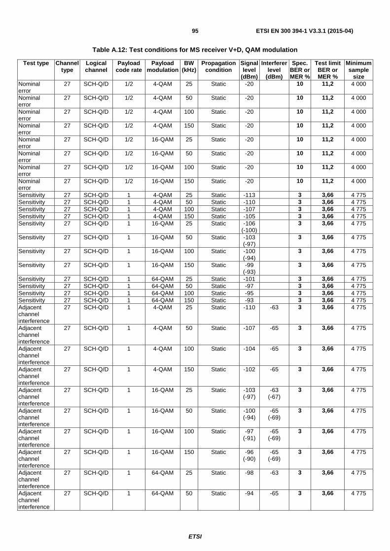
ETSI
ETSI EN 300 394-1 V3.3.1 (2015-04)95
Table A.12: Test conditions for MS receiver V+D, QAM modulation
Test type Channel type
Logical channel
Payload code rate
Payload modulation
BW (kHz)
Propagation condition
Signal level
(dBm)
Interferer level
(dBm)
Spec. BER or MER %
Test limit BER or MER %
Minimum sample
size Nominal error
27 SCH-Q/D 1/2 4-QAM 25 Static -20 10 11,2 4 000
Nominal error
27 SCH-Q/D 1/2 4-QAM 50 Static -20 10 11,2 4 000
Nominal error
27 SCH-Q/D 1/2 4-QAM 100 Static -20 10 11,2 4 000
Nominal error
27 SCH-Q/D 1/2 4-QAM 150 Static -20 10 11,2 4 000
Nominal error
27 SCH-Q/D 1/2 16-QAM 25 Static -20 10 11,2 4 000
Nominal error
27 SCH-Q/D 1/2 16-QAM 50 Static -20 10 11,2 4 000
Nominal error
27 SCH-Q/D 1/2 16-QAM 100 Static -20 10 11,2 4 000
Nominal error
27 SCH-Q/D 1/2 16-QAM 150 Static -20 10 11,2 4 000
Sensitivity 27 SCH-Q/D 1 4-QAM 25 Static -113 3 3,66 4 775 Sensitivity 27 SCH-Q/D 1 4-QAM 50 Static -110 3 3,66 4 775 Sensitivity 27 SCH-Q/D 1 4-QAM 100 Static -107 3 3,66 4 775 Sensitivity 27 SCH-Q/D 1 4-QAM 150 Static -105 3 3,66 4 775 Sensitivity 27 SCH-Q/D 1 16-QAM 25 Static -106
(-100) 3 3,66 4 775
Sensitivity 27 SCH-Q/D 1 16-QAM 50 Static -103 (-97)
3 3,66 4 775
Sensitivity 27 SCH-Q/D 1 16-QAM 100 Static -100 (-94)
3 3,66 4 775
Sensitivity 27 SCH-Q/D 1 16-QAM 150 Static -99 (-93)
3 3,66 4 775
Sensitivity 27 SCH-Q/D 1 64-QAM 25 Static -101 3 3,66 4 775 Sensitivity 27 SCH-Q/D 1 64-QAM 50 Static -97 3 3,66 4 775 Sensitivity 27 SCH-Q/D 1 64-QAM 100 Static -95 3 3,66 4 775 Sensitivity 27 SCH-Q/D 1 64-QAM 150 Static -93 3 3,66 4 775 Adjacent channel interference
27 SCH-Q/D 1 4-QAM 25 Static -110 -63 3 3,66 4 775
Adjacent channel interference
27 SCH-Q/D 1 4-QAM 50 Static -107 -65 3 3,66 4 775
Adjacent channel interference
27 SCH-Q/D 1 4-QAM 100 Static -104 -65 3 3,66 4 775
Adjacent channel interference
27 SCH-Q/D 1 4-QAM 150 Static -102 -65 3 3,66 4 775
Adjacent channel interference
27 SCH-Q/D 1 16-QAM 25 Static -103 (-97)
-63 (-67)
3 3,66 4 775
Adjacent channel interference
27 SCH-Q/D 1 16-QAM 50 Static -100 (-94)
-65 (-69)
3 3,66 4 775
Adjacent channel interference
27 SCH-Q/D 1 16-QAM 100 Static -97 (-91)
-65 (-69)
3 3,66 4 775
Adjacent channel interference
27 SCH-Q/D 1 16-QAM 150 Static -96 (-90)
-65 (-69)
3 3,66 4 775
Adjacent channel interference
27 SCH-Q/D 1 64-QAM 25 Static -98 -63 3 3,66 4 775
Adjacent channel interference
27 SCH-Q/D 1 64-QAM 50 Static -94 -65 3 3,66 4 775
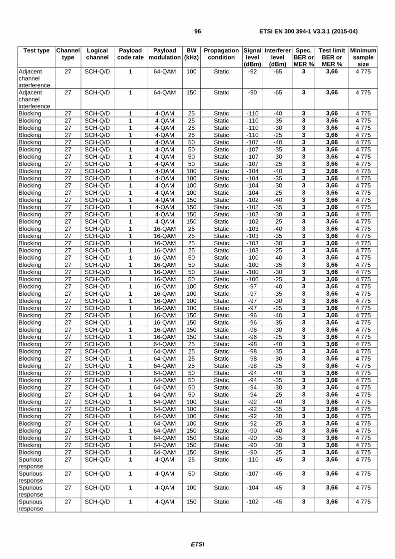
ETSI
ETSI EN 300 394-1 V3.3.1 (2015-04)96
Test type Channel type
Logical channel
Payload code rate
Payload modulation
BW (kHz)
Propagation condition
Signal level
(dBm)
Interferer level
(dBm)
Spec. BER or MER %
Test limit BER or MER %
Minimum sample
size Adjacent channel interference
27 SCH-Q/D 1 64-QAM 100 Static -92 -65 3 3,66 4 775
Adjacent channel interference
27 SCH-Q/D 1 64-QAM 150 Static -90 -65 3 3,66 4 775
Blocking 27 SCH-Q/D 1 4-QAM 25 Static -110 -40 3 3,66 4 775 Blocking 27 SCH-Q/D 1 4-QAM 25 Static -110 -35 3 3,66 4 775 Blocking 27 SCH-Q/D 1 4-QAM 25 Static -110 -30 3 3,66 4 775 Blocking 27 SCH-Q/D 1 4-QAM 25 Static -110 -25 3 3,66 4 775 Blocking 27 SCH-Q/D 1 4-QAM 50 Static -107 -40 3 3,66 4 775 Blocking 27 SCH-Q/D 1 4-QAM 50 Static -107 -35 3 3,66 4 775 Blocking 27 SCH-Q/D 1 4-QAM 50 Static -107 -30 3 3,66 4 775 Blocking 27 SCH-Q/D 1 4-QAM 50 Static -107 -25 3 3,66 4 775 Blocking 27 SCH-Q/D 1 4-QAM 100 Static -104 -40 3 3,66 4 775 Blocking 27 SCH-Q/D 1 4-QAM 100 Static -104 -35 3 3,66 4 775 Blocking 27 SCH-Q/D 1 4-QAM 100 Static -104 -30 3 3,66 4 775 Blocking 27 SCH-Q/D 1 4-QAM 100 Static -104 -25 3 3,66 4 775 Blocking 27 SCH-Q/D 1 4-QAM 150 Static -102 -40 3 3,66 4 775 Blocking 27 SCH-Q/D 1 4-QAM 150 Static -102 -35 3 3,66 4 775 Blocking 27 SCH-Q/D 1 4-QAM 150 Static -102 -30 3 3,66 4 775 Blocking 27 SCH-Q/D 1 4-QAM 150 Static -102 -25 3 3,66 4 775 Blocking 27 SCH-Q/D 1 16-QAM 25 Static -103 -40 3 3,66 4 775 Blocking 27 SCH-Q/D 1 16-QAM 25 Static -103 -35 3 3,66 4 775 Blocking 27 SCH-Q/D 1 16-QAM 25 Static -103 -30 3 3,66 4 775 Blocking 27 SCH-Q/D 1 16-QAM 25 Static -103 -25 3 3,66 4 775 Blocking 27 SCH-Q/D 1 16-QAM 50 Static -100 -40 3 3,66 4 775 Blocking 27 SCH-Q/D 1 16-QAM 50 Static -100 -35 3 3,66 4 775 Blocking 27 SCH-Q/D 1 16-QAM 50 Static -100 -30 3 3,66 4 775 Blocking 27 SCH-Q/D 1 16-QAM 50 Static -100 -25 3 3,66 4 775 Blocking 27 SCH-Q/D 1 16-QAM 100 Static -97 -40 3 3,66 4 775 Blocking 27 SCH-Q/D 1 16-QAM 100 Static -97 -35 3 3,66 4 775 Blocking 27 SCH-Q/D 1 16-QAM 100 Static -97 -30 3 3,66 4 775 Blocking 27 SCH-Q/D 1 16-QAM 100 Static -97 -25 3 3,66 4 775 Blocking 27 SCH-Q/D 1 16-QAM 150 Static -96 -40 3 3,66 4 775 Blocking 27 SCH-Q/D 1 16-QAM 150 Static -96 -35 3 3,66 4 775 Blocking 27 SCH-Q/D 1 16-QAM 150 Static -96 -30 3 3,66 4 775 Blocking 27 SCH-Q/D 1 16-QAM 150 Static -96 -25 3 3,66 4 775 Blocking 27 SCH-Q/D 1 64-QAM 25 Static -98 -40 3 3,66 4 775 Blocking 27 SCH-Q/D 1 64-QAM 25 Static -98 -35 3 3,66 4 775 Blocking 27 SCH-Q/D 1 64-QAM 25 Static -98 -30 3 3,66 4 775 Blocking 27 SCH-Q/D 1 64-QAM 25 Static -98 -25 3 3,66 4 775 Blocking 27 SCH-Q/D 1 64-QAM 50 Static -94 -40 3 3,66 4 775 Blocking 27 SCH-Q/D 1 64-QAM 50 Static -94 -35 3 3,66 4 775 Blocking 27 SCH-Q/D 1 64-QAM 50 Static -94 -30 3 3,66 4 775 Blocking 27 SCH-Q/D 1 64-QAM 50 Static -94 -25 3 3,66 4 775 Blocking 27 SCH-Q/D 1 64-QAM 100 Static -92 -40 3 3,66 4 775 Blocking 27 SCH-Q/D 1 64-QAM 100 Static -92 -35 3 3,66 4 775 Blocking 27 SCH-Q/D 1 64-QAM 100 Static -92 -30 3 3,66 4 775 Blocking 27 SCH-Q/D 1 64-QAM 100 Static -92 -25 3 3,66 4 775 Blocking 27 SCH-Q/D 1 64-QAM 150 Static -90 -40 3 3,66 4 775 Blocking 27 SCH-Q/D 1 64-QAM 150 Static -90 -35 3 3,66 4 775 Blocking 27 SCH-Q/D 1 64-QAM 150 Static -90 -30 3 3,66 4 775 Blocking 27 SCH-Q/D 1 64-QAM 150 Static -90 -25 3 3,66 4 775 Spurious response
27 SCH-Q/D 1 4-QAM 25 Static -110 -45 3 3,66 4 775
Spurious response
27 SCH-Q/D 1 4-QAM 50 Static -107 -45 3 3,66 4 775
Spurious response
27 SCH-Q/D 1 4-QAM 100 Static -104 -45 3 3,66 4 775
Spurious response
27 SCH-Q/D 1 4-QAM 150 Static -102 -45 3 3,66 4 775
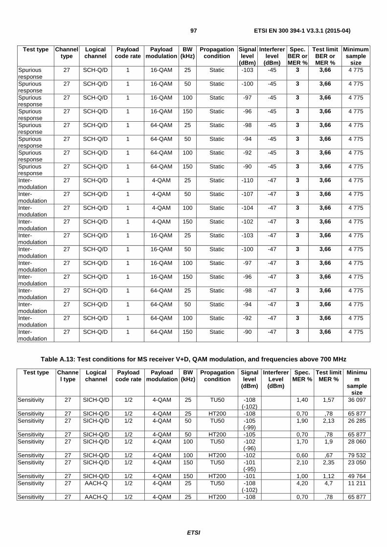
ETSI
ETSI EN 300 394-1 V3.3.1 (2015-04)97
Test type Channel type
Logical channel
Payload code rate
Payload modulation
BW (kHz)
Propagation condition
Signal level
(dBm)
Interferer level
(dBm)
Spec. BER or MER %
Test limit BER or MER %
Minimum sample
size Spurious response
27 SCH-Q/D 1 16-QAM 25 Static -103 -45 3 3,66 4 775
Spurious response
27 SCH-Q/D 1 16-QAM 50 Static -100 -45 3 3,66 4 775
Spurious response
27 SCH-Q/D 1 16-QAM 100 Static -97 -45 3 3,66 4 775
Spurious response
27 SCH-Q/D 1 16-QAM 150 Static -96 -45 3 3,66 4 775
Spurious response
27 SCH-Q/D 1 64-QAM 25 Static -98 -45 3 3,66 4 775
Spurious response
27 SCH-Q/D 1 64-QAM 50 Static -94 -45 3 3,66 4 775
Spurious response
27 SCH-Q/D 1 64-QAM 100 Static -92 -45 3 3,66 4 775
Spurious response
27 SCH-Q/D 1 64-QAM 150 Static -90 -45 3 3,66 4 775
Inter-modulation
27 SCH-Q/D 1 4-QAM 25 Static -110 -47 3 3,66 4 775
Inter-modulation
27 SCH-Q/D 1 4-QAM 50 Static -107 -47 3 3,66 4 775
Inter-modulation
27 SCH-Q/D 1 4-QAM 100 Static -104 -47 3 3,66 4 775
Inter-modulation
27 SCH-Q/D 1 4-QAM 150 Static -102 -47 3 3,66 4 775
Inter-modulation
27 SCH-Q/D 1 16-QAM 25 Static -103 -47 3 3,66 4 775
Inter-modulation
27 SCH-Q/D 1 16-QAM 50 Static -100 -47 3 3,66 4 775
Inter-modulation
27 SCH-Q/D 1 16-QAM 100 Static -97 -47 3 3,66 4 775
Inter-modulation
27 SCH-Q/D 1 16-QAM 150 Static -96 -47 3 3,66 4 775
Inter-modulation
27 SCH-Q/D 1 64-QAM 25 Static -98 -47 3 3,66 4 775
Inter-modulation
27 SCH-Q/D 1 64-QAM 50 Static -94 -47 3 3,66 4 775
Inter-modulation
27 SCH-Q/D 1 64-QAM 100 Static -92 -47 3 3,66 4 775
Inter-modulation
27 SCH-Q/D 1 64-QAM 150 Static -90 -47 3 3,66 4 775
Table A.13: Test conditions for MS receiver V+D, QAM modulation, and frequencies above 700 MHz
Test type Channel type
Logical channel
Payload code rate
Payload modulation
BW (kHz)
Propagation condition
Signal level
(dBm)
Interferer Level (dBm)
Spec. MER %
Test limit MER %
Minimum
sample size
Sensitivity 27 SICH-Q/D 1/2 4-QAM 25 TU50 -108 (-102)
1,40 1,57 36 097
Sensitivity 27 SICH-Q/D 1/2 4-QAM 25 HT200 -108 0,70 ,78 65 877 Sensitivity 27 SICH-Q/D 1/2 4-QAM 50 TU50 -105
(-99) 1,90 2,13 26 285
Sensitivity 27 SICH-Q/D 1/2 4-QAM 50 HT200 -105 0,70 ,78 65 877 Sensitivity 27 SICH-Q/D 1/2 4-QAM 100 TU50 -102
(-96) 1,70 1,9 28 060
Sensitivity 27 SICH-Q/D 1/2 4-QAM 100 HT200 -102 0,60 ,67 79 532 Sensitivity 27 SICH-Q/D 1/2 4-QAM 150 TU50 -101
(-95) 2,10 2,35 23 050
Sensitivity 27 SICH-Q/D 1/2 4-QAM 150 HT200 -101 1,00 1,12 49 764 Sensitivity 27 AACH-Q 1/2 4-QAM 25 TU50 -108
(-102) 4,20 4,7 11 211
Sensitivity 27 AACH-Q 1/2 4-QAM 25 HT200 -108 0,70 ,78 65 877
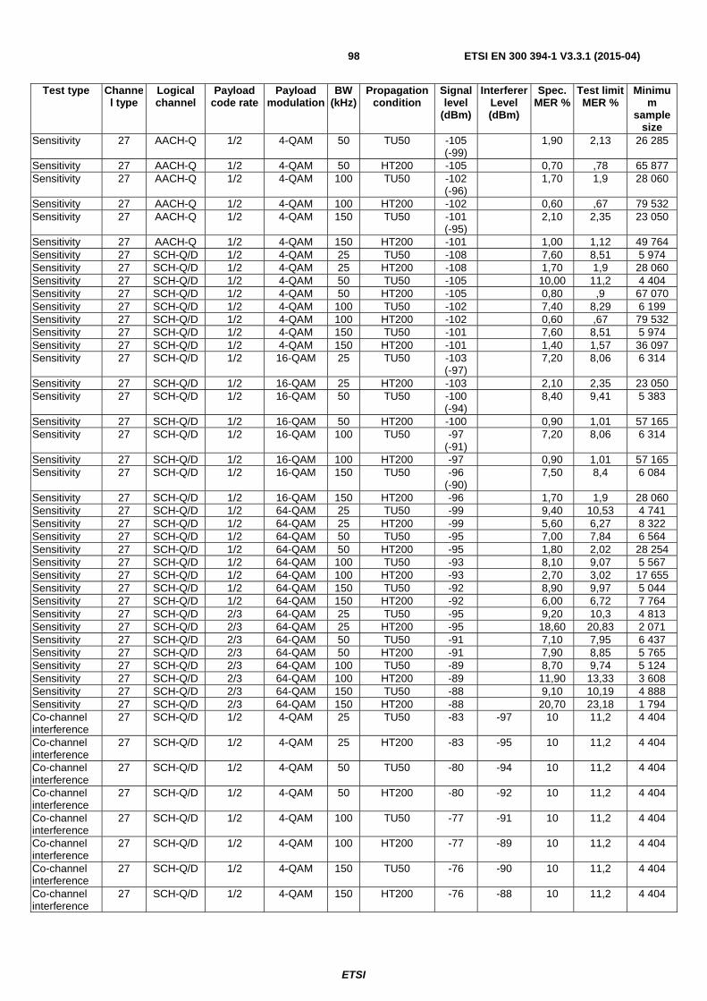
ETSI
ETSI EN 300 394-1 V3.3.1 (2015-04)98
Test type Channel type
Logical channel
Payload code rate
Payload modulation
BW (kHz)
Propagation condition
Signal level
(dBm)
Interferer Level (dBm)
Spec. MER %
Test limit MER %
Minimum
sample size
Sensitivity 27 AACH-Q 1/2 4-QAM 50 TU50 -105 (-99)
1,90 2,13 26 285
Sensitivity 27 AACH-Q 1/2 4-QAM 50 HT200 -105 0,70 ,78 65 877 Sensitivity 27 AACH-Q 1/2 4-QAM 100 TU50 -102
(-96) 1,70 1,9 28 060
Sensitivity 27 AACH-Q 1/2 4-QAM 100 HT200 -102 0,60 ,67 79 532 Sensitivity 27 AACH-Q 1/2 4-QAM 150 TU50 -101
(-95) 2,10 2,35 23 050
Sensitivity 27 AACH-Q 1/2 4-QAM 150 HT200 -101 1,00 1,12 49 764 Sensitivity 27 SCH-Q/D 1/2 4-QAM 25 TU50 -108 7,60 8,51 5 974 Sensitivity 27 SCH-Q/D 1/2 4-QAM 25 HT200 -108 1,70 1,9 28 060 Sensitivity 27 SCH-Q/D 1/2 4-QAM 50 TU50 -105 10,00 11,2 4 404 Sensitivity 27 SCH-Q/D 1/2 4-QAM 50 HT200 -105 0,80 ,9 67 070 Sensitivity 27 SCH-Q/D 1/2 4-QAM 100 TU50 -102 7,40 8,29 6 199 Sensitivity 27 SCH-Q/D 1/2 4-QAM 100 HT200 -102 0,60 ,67 79 532 Sensitivity 27 SCH-Q/D 1/2 4-QAM 150 TU50 -101 7,60 8,51 5 974 Sensitivity 27 SCH-Q/D 1/2 4-QAM 150 HT200 -101 1,40 1,57 36 097 Sensitivity 27 SCH-Q/D 1/2 16-QAM 25 TU50 -103
(-97) 7,20 8,06 6 314
Sensitivity 27 SCH-Q/D 1/2 16-QAM 25 HT200 -103 2,10 2,35 23 050 Sensitivity 27 SCH-Q/D 1/2 16-QAM 50 TU50 -100
(-94) 8,40 9,41 5 383
Sensitivity 27 SCH-Q/D 1/2 16-QAM 50 HT200 -100 0,90 1,01 57 165 Sensitivity 27 SCH-Q/D 1/2 16-QAM 100 TU50 -97
(-91) 7,20 8,06 6 314
Sensitivity 27 SCH-Q/D 1/2 16-QAM 100 HT200 -97 0,90 1,01 57 165 Sensitivity 27 SCH-Q/D 1/2 16-QAM 150 TU50 -96
(-90) 7,50 8,4 6 084
Sensitivity 27 SCH-Q/D 1/2 16-QAM 150 HT200 -96 1,70 1,9 28 060 Sensitivity 27 SCH-Q/D 1/2 64-QAM 25 TU50 -99 9,40 10,53 4 741 Sensitivity 27 SCH-Q/D 1/2 64-QAM 25 HT200 -99 5,60 6,27 8 322 Sensitivity 27 SCH-Q/D 1/2 64-QAM 50 TU50 -95 7,00 7,84 6 564 Sensitivity 27 SCH-Q/D 1/2 64-QAM 50 HT200 -95 1,80 2,02 28 254 Sensitivity 27 SCH-Q/D 1/2 64-QAM 100 TU50 -93 8,10 9,07 5 567 Sensitivity 27 SCH-Q/D 1/2 64-QAM 100 HT200 -93 2,70 3,02 17 655 Sensitivity 27 SCH-Q/D 1/2 64-QAM 150 TU50 -92 8,90 9,97 5 044 Sensitivity 27 SCH-Q/D 1/2 64-QAM 150 HT200 -92 6,00 6,72 7 764 Sensitivity 27 SCH-Q/D 2/3 64-QAM 25 TU50 -95 9,20 10,3 4 813 Sensitivity 27 SCH-Q/D 2/3 64-QAM 25 HT200 -95 18,60 20,83 2 071 Sensitivity 27 SCH-Q/D 2/3 64-QAM 50 TU50 -91 7,10 7,95 6 437 Sensitivity 27 SCH-Q/D 2/3 64-QAM 50 HT200 -91 7,90 8,85 5 765 Sensitivity 27 SCH-Q/D 2/3 64-QAM 100 TU50 -89 8,70 9,74 5 124 Sensitivity 27 SCH-Q/D 2/3 64-QAM 100 HT200 -89 11,90 13,33 3 608 Sensitivity 27 SCH-Q/D 2/3 64-QAM 150 TU50 -88 9,10 10,19 4 888 Sensitivity 27 SCH-Q/D 2/3 64-QAM 150 HT200 -88 20,70 23,18 1 794 Co-channel interference
27 SCH-Q/D 1/2 4-QAM 25 TU50 -83 -97 10 11,2 4 404
Co-channel interference
27 SCH-Q/D 1/2 4-QAM 25 HT200 -83 -95 10 11,2 4 404
Co-channel interference
27 SCH-Q/D 1/2 4-QAM 50 TU50 -80 -94 10 11,2 4 404
Co-channel interference
27 SCH-Q/D 1/2 4-QAM 50 HT200 -80 -92 10 11,2 4 404
Co-channel interference
27 SCH-Q/D 1/2 4-QAM 100 TU50 -77 -91 10 11,2 4 404
Co-channel interference
27 SCH-Q/D 1/2 4-QAM 100 HT200 -77 -89 10 11,2 4 404
Co-channel interference
27 SCH-Q/D 1/2 4-QAM 150 TU50 -76 -90 10 11,2 4 404
Co-channel interference
27 SCH-Q/D 1/2 4-QAM 150 HT200 -76 -88 10 11,2 4 404
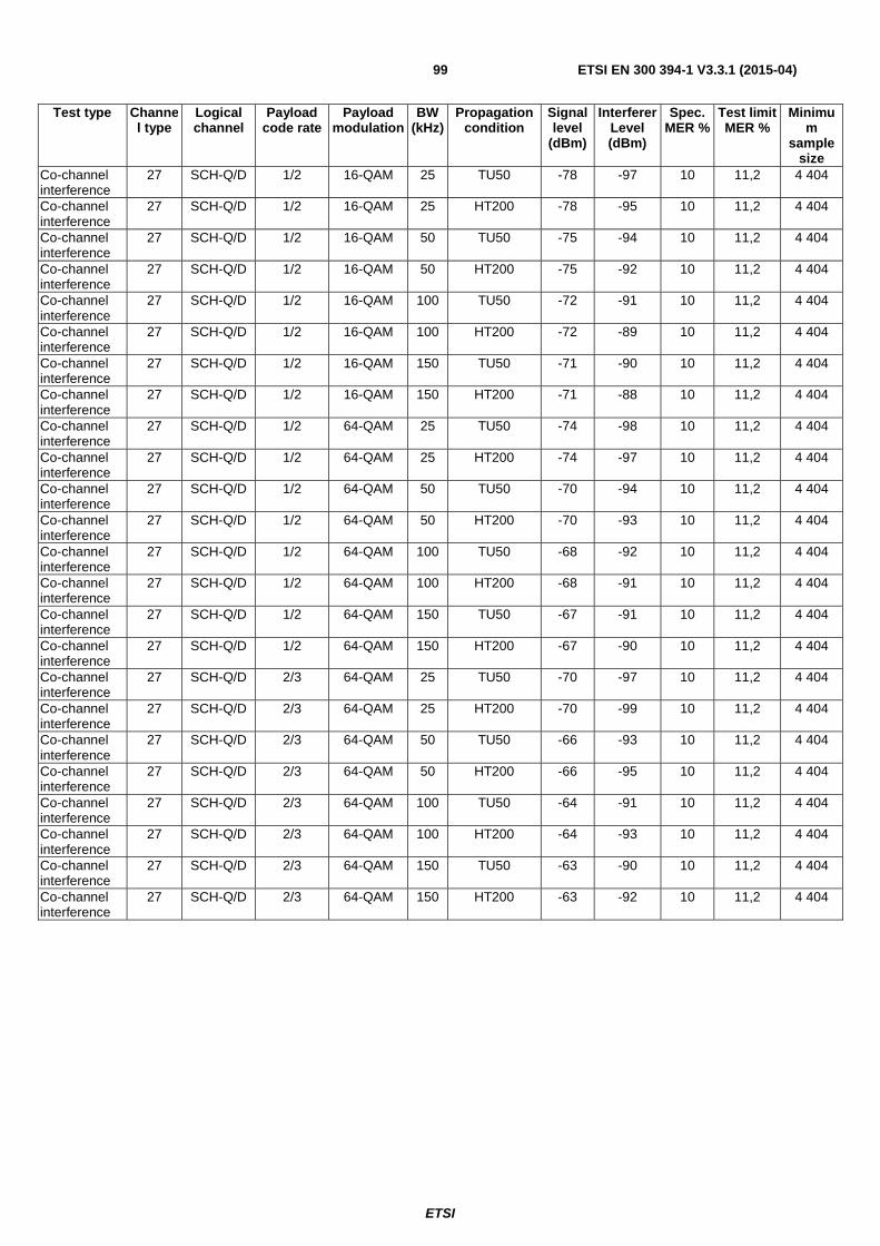
ETSI
ETSI EN 300 394-1 V3.3.1 (2015-04)99
Test type Channel type
Logical channel
Payload code rate
Payload modulation
BW (kHz)
Propagation condition
Signal level
(dBm)
Interferer Level (dBm)
Spec. MER %
Test limit MER %
Minimum
sample size
Co-channel interference
27 SCH-Q/D 1/2 16-QAM 25 TU50 -78 -97 10 11,2 4 404
Co-channel interference
27 SCH-Q/D 1/2 16-QAM 25 HT200 -78 -95 10 11,2 4 404
Co-channel interference
27 SCH-Q/D 1/2 16-QAM 50 TU50 -75 -94 10 11,2 4 404
Co-channel interference
27 SCH-Q/D 1/2 16-QAM 50 HT200 -75 -92 10 11,2 4 404
Co-channel interference
27 SCH-Q/D 1/2 16-QAM 100 TU50 -72 -91 10 11,2 4 404
Co-channel interference
27 SCH-Q/D 1/2 16-QAM 100 HT200 -72 -89 10 11,2 4 404
Co-channel interference
27 SCH-Q/D 1/2 16-QAM 150 TU50 -71 -90 10 11,2 4 404
Co-channel interference
27 SCH-Q/D 1/2 16-QAM 150 HT200 -71 -88 10 11,2 4 404
Co-channel interference
27 SCH-Q/D 1/2 64-QAM 25 TU50 -74 -98 10 11,2 4 404
Co-channel interference
27 SCH-Q/D 1/2 64-QAM 25 HT200 -74 -97 10 11,2 4 404
Co-channel interference
27 SCH-Q/D 1/2 64-QAM 50 TU50 -70 -94 10 11,2 4 404
Co-channel interference
27 SCH-Q/D 1/2 64-QAM 50 HT200 -70 -93 10 11,2 4 404
Co-channel interference
27 SCH-Q/D 1/2 64-QAM 100 TU50 -68 -92 10 11,2 4 404
Co-channel interference
27 SCH-Q/D 1/2 64-QAM 100 HT200 -68 -91 10 11,2 4 404
Co-channel interference
27 SCH-Q/D 1/2 64-QAM 150 TU50 -67 -91 10 11,2 4 404
Co-channel interference
27 SCH-Q/D 1/2 64-QAM 150 HT200 -67 -90 10 11,2 4 404
Co-channel interference
27 SCH-Q/D 2/3 64-QAM 25 TU50 -70 -97 10 11,2 4 404
Co-channel interference
27 SCH-Q/D 2/3 64-QAM 25 HT200 -70 -99 10 11,2 4 404
Co-channel interference
27 SCH-Q/D 2/3 64-QAM 50 TU50 -66 -93 10 11,2 4 404
Co-channel interference
27 SCH-Q/D 2/3 64-QAM 50 HT200 -66 -95 10 11,2 4 404
Co-channel interference
27 SCH-Q/D 2/3 64-QAM 100 TU50 -64 -91 10 11,2 4 404
Co-channel interference
27 SCH-Q/D 2/3 64-QAM 100 HT200 -64 -93 10 11,2 4 404
Co-channel interference
27 SCH-Q/D 2/3 64-QAM 150 TU50 -63 -90 10 11,2 4 404
Co-channel interference
27 SCH-Q/D 2/3 64-QAM 150 HT200 -63 -92 10 11,2 4 404
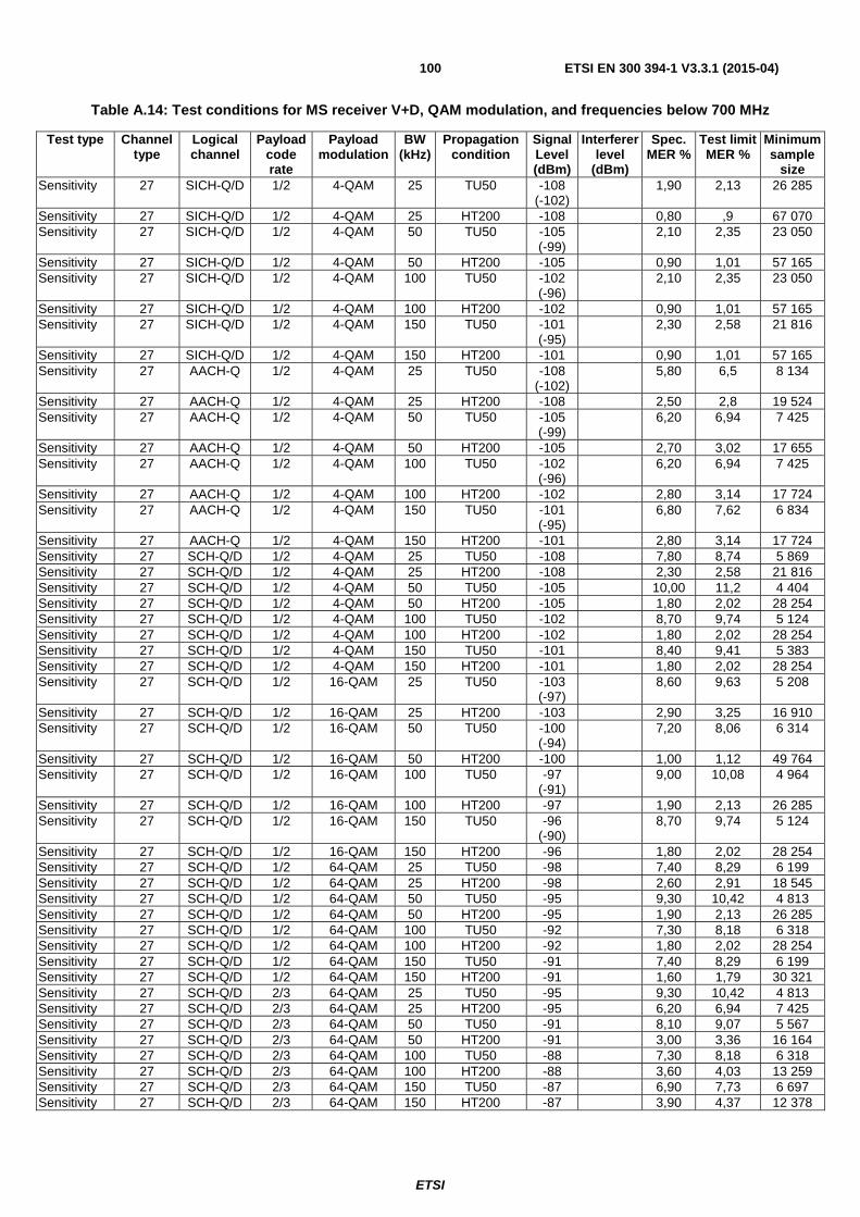
ETSI
ETSI EN 300 394-1 V3.3.1 (2015-04)100
Table A.14: Test conditions for MS receiver V+D, QAM modulation, and frequencies below 700 MHz
Test type Channel type
Logical channel
Payload code rate
Payload modulation
BW (kHz)
Propagation condition
Signal Level (dBm)
Interferer level
(dBm)
Spec. MER %
Test limit MER %
Minimum sample
size Sensitivity 27 SICH-Q/D 1/2 4-QAM 25 TU50 -108
(-102) 1,90 2,13 26 285
Sensitivity 27 SICH-Q/D 1/2 4-QAM 25 HT200 -108 0,80 ,9 67 070 Sensitivity 27 SICH-Q/D 1/2 4-QAM 50 TU50 -105
(-99) 2,10 2,35 23 050
Sensitivity 27 SICH-Q/D 1/2 4-QAM 50 HT200 -105 0,90 1,01 57 165 Sensitivity 27 SICH-Q/D 1/2 4-QAM 100 TU50 -102
(-96) 2,10 2,35 23 050
Sensitivity 27 SICH-Q/D 1/2 4-QAM 100 HT200 -102 0,90 1,01 57 165 Sensitivity 27 SICH-Q/D 1/2 4-QAM 150 TU50 -101
(-95) 2,30 2,58 21 816
Sensitivity 27 SICH-Q/D 1/2 4-QAM 150 HT200 -101 0,90 1,01 57 165 Sensitivity 27 AACH-Q 1/2 4-QAM 25 TU50 -108
(-102) 5,80 6,5 8 134
Sensitivity 27 AACH-Q 1/2 4-QAM 25 HT200 -108 2,50 2,8 19 524 Sensitivity 27 AACH-Q 1/2 4-QAM 50 TU50 -105
(-99) 6,20 6,94 7 425
Sensitivity 27 AACH-Q 1/2 4-QAM 50 HT200 -105 2,70 3,02 17 655 Sensitivity 27 AACH-Q 1/2 4-QAM 100 TU50 -102
(-96) 6,20 6,94 7 425
Sensitivity 27 AACH-Q 1/2 4-QAM 100 HT200 -102 2,80 3,14 17 724 Sensitivity 27 AACH-Q 1/2 4-QAM 150 TU50 -101
(-95) 6,80 7,62 6 834
Sensitivity 27 AACH-Q 1/2 4-QAM 150 HT200 -101 2,80 3,14 17 724 Sensitivity 27 SCH-Q/D 1/2 4-QAM 25 TU50 -108 7,80 8,74 5 869 Sensitivity 27 SCH-Q/D 1/2 4-QAM 25 HT200 -108 2,30 2,58 21 816 Sensitivity 27 SCH-Q/D 1/2 4-QAM 50 TU50 -105 10,00 11,2 4 404 Sensitivity 27 SCH-Q/D 1/2 4-QAM 50 HT200 -105 1,80 2,02 28 254 Sensitivity 27 SCH-Q/D 1/2 4-QAM 100 TU50 -102 8,70 9,74 5 124 Sensitivity 27 SCH-Q/D 1/2 4-QAM 100 HT200 -102 1,80 2,02 28 254 Sensitivity 27 SCH-Q/D 1/2 4-QAM 150 TU50 -101 8,40 9,41 5 383 Sensitivity 27 SCH-Q/D 1/2 4-QAM 150 HT200 -101 1,80 2,02 28 254 Sensitivity 27 SCH-Q/D 1/2 16-QAM 25 TU50 -103
(-97) 8,60 9,63 5 208
Sensitivity 27 SCH-Q/D 1/2 16-QAM 25 HT200 -103 2,90 3,25 16 910 Sensitivity 27 SCH-Q/D 1/2 16-QAM 50 TU50 -100
(-94) 7,20 8,06 6 314
Sensitivity 27 SCH-Q/D 1/2 16-QAM 50 HT200 -100 1,00 1,12 49 764 Sensitivity 27 SCH-Q/D 1/2 16-QAM 100 TU50 -97
(-91) 9,00 10,08 4 964
Sensitivity 27 SCH-Q/D 1/2 16-QAM 100 HT200 -97 1,90 2,13 26 285 Sensitivity 27 SCH-Q/D 1/2 16-QAM 150 TU50 -96
(-90) 8,70 9,74 5 124
Sensitivity 27 SCH-Q/D 1/2 16-QAM 150 HT200 -96 1,80 2,02 28 254 Sensitivity 27 SCH-Q/D 1/2 64-QAM 25 TU50 -98 7,40 8,29 6 199 Sensitivity 27 SCH-Q/D 1/2 64-QAM 25 HT200 -98 2,60 2,91 18 545 Sensitivity 27 SCH-Q/D 1/2 64-QAM 50 TU50 -95 9,30 10,42 4 813 Sensitivity 27 SCH-Q/D 1/2 64-QAM 50 HT200 -95 1,90 2,13 26 285 Sensitivity 27 SCH-Q/D 1/2 64-QAM 100 TU50 -92 7,30 8,18 6 318 Sensitivity 27 SCH-Q/D 1/2 64-QAM 100 HT200 -92 1,80 2,02 28 254 Sensitivity 27 SCH-Q/D 1/2 64-QAM 150 TU50 -91 7,40 8,29 6 199 Sensitivity 27 SCH-Q/D 1/2 64-QAM 150 HT200 -91 1,60 1,79 30 321 Sensitivity 27 SCH-Q/D 2/3 64-QAM 25 TU50 -95 9,30 10,42 4 813 Sensitivity 27 SCH-Q/D 2/3 64-QAM 25 HT200 -95 6,20 6,94 7 425 Sensitivity 27 SCH-Q/D 2/3 64-QAM 50 TU50 -91 8,10 9,07 5 567 Sensitivity 27 SCH-Q/D 2/3 64-QAM 50 HT200 -91 3,00 3,36 16 164 Sensitivity 27 SCH-Q/D 2/3 64-QAM 100 TU50 -88 7,30 8,18 6 318 Sensitivity 27 SCH-Q/D 2/3 64-QAM 100 HT200 -88 3,60 4,03 13 259 Sensitivity 27 SCH-Q/D 2/3 64-QAM 150 TU50 -87 6,90 7,73 6 697 Sensitivity 27 SCH-Q/D 2/3 64-QAM 150 HT200 -87 3,90 4,37 12 378

ETSI
ETSI EN 300 394-1 V3.3.1 (2015-04)101
Test type Channel type
Logical channel
Payload code rate
Payload modulation
BW (kHz)
Propagation condition
Signal Level (dBm)
Interferer level
(dBm)
Spec. MER %
Test limit MER %
Minimum sample
size Co-channel interference
27 SCH-Q/D 1/2 4-QAM 25 TU50 -83 -97 10 11,2 4 404
Co-channel interference
27 SCH-Q/D 1/2 4-QAM 25 HT200 -83 -95 10 11,2 4 404
Co-channel interference
27 SCH-Q/D 1/2 4-QAM 50 TU50 -80 -94 10 11,2 4 404
Co-channel interference
27 SCH-Q/D 1/2 4-QAM 50 HT200 -80 -92 10 11,2 4 404
Co-channel interference
27 SCH-Q/D 1/2 4-QAM 100 TU50 -77 -91 10 11,2 4 404
Co-channel interference
27 SCH-Q/D 1/2 4-QAM 100 HT200 -77 -89 10 11,2 4 404
Co-channel interference
27 SCH-Q/D 1/2 4-QAM 150 TU50 -76 -90 10 11,2 4 404
Co-channel interference
27 SCH-Q/D 1/2 4-QAM 150 HT200 -76 -88 10 11,2 4 404
Co-channel interference
27 SCH-Q/D 1/2 16-QAM 25 TU50 -78 -97 10 11,2 4 404
Co-channel interference
27 SCH-Q/D 1/2 16-QAM 25 HT200 -78 -95 10 11,2 4 404
Co-channel interference
27 SCH-Q/D 1/2 16-QAM 50 TU50 -75 -94 10 11,2 4 404
Co-channel interference
27 SCH-Q/D 1/2 16-QAM 50 HT200 -75 -92 10 11,2 4 404
Co-channel interference
27 SCH-Q/D 1/2 16-QAM 100 TU50 -72 -91 10 11,2 4 404
Co-channel interference
27 SCH-Q/D 1/2 16-QAM 100 HT200 -72 -89 10 11,2 4 404
Co-channel interference
27 SCH-Q/D 1/2 16-QAM 150 TU50 -71 -90 10 11,2 4 404
Co-channel interference
27 SCH-Q/D 1/2 16-QAM 150 HT200 -71 -88 10 11,2 4 404
Co-channel interference
27 SCH-Q/D 1/2 64-QAM 25 TU50 -73 -96 10 11,2 4 404
Co-channel interference
27 SCH-Q/D 1/2 64-QAM 25 HT200 -73 -95 10 11,2 4 404
Co-channel interference
27 SCH-Q/D 1/2 64-QAM 50 TU50 -70 -93 10 11,2 4 404
Co-channel interference
27 SCH-Q/D 1/2 64-QAM 50 HT200 -70 -92 10 11,2 4 404
Co-channel interference
27 SCH-Q/D 1/2 64-QAM 100 TU50 -67 -90 10 11,2 4 404
Co-channel interference
27 SCH-Q/D 1/2 64-QAM 100 HT200 -67 -89 10 11,2 4 404
Co-channel interference
27 SCH-Q/D 1/2 64-QAM 150 TU50 -66 -89 10 11,2 4 404
Co-channel interference
27 SCH-Q/D 1/2 64-QAM 150 HT200 -66 -88 10 11,2 4 404
Co-channel interference
27 SCH-Q/D 2/3 64-QAM 25 TU50 -70 -97 10 11,2 4 404
Co-channel interference
27 SCH-Q/D 2/3 64-QAM 25 HT200 -70 -96 10 11,2 4 404
Co-channel interference
27 SCH-Q/D 2/3 64-QAM 50 TU50 -66 -93 10 11,2 4 404
Co-channel interference
27 SCH-Q/D 2/3 64-QAM 50 HT200 -66 -92 10 11,2 4 404
Co-channel interference
27 SCH-Q/D 2/3 64-QAM 100 TU50 -63 -90 10 11,2 4 404
Co-channel interference
27 SCH-Q/D 2/3 64-QAM 100 HT200 -63 -89 10 11,2 4 404
Co-channel interference
27 SCH-Q/D 2/3 64-QAM 150 TU50 -62 -89 10 11,2 4 404
Co-channel interference
27 SCH-Q/D 2/3 64-QAM 150 HT200 -62 -88 10 11,2 4 404
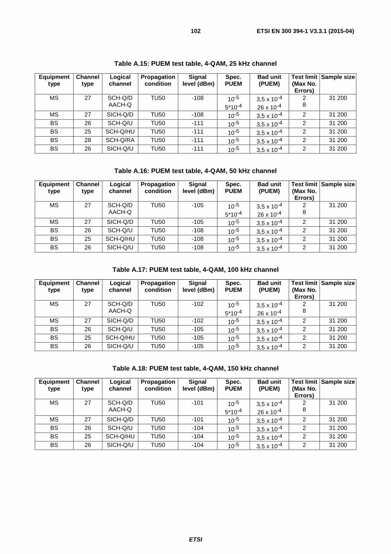
ETSI
ETSI EN 300 394-1 V3.3.1 (2015-04)102
Table A.15: PUEM test table, 4-QAM, 25 kHz channel
Equipment type
Channel type
Logical channel
Propagation condition
Signal level (dBm)
Spec. PUEM
Bad unit (PUEM)
Test limit (Max No. Errors)
Sample size
MS 27 SCH-Q/D AACH-Q
TU50 -108 10-5
5*10-4 3,5 x 10⁻⁴
26 x 10-4
2 8
31 200
MS 27 SICH-Q/D TU50 -108 10-5 3,5 x 10⁻⁴ 2 31 200 BS 26 SCH-Q/U TU50 -111 10-5 3,5 x 10⁻⁴ 2 31 200 BS 25 SCH-Q/HU TU50 -111 10-5 3,5 x 10⁻⁴ 2 31 200 BS 28 SCH-Q/RA TU50 -111 10-5 3,5 x 10⁻⁴ 2 31 200 BS 26 SICH-Q/U TU50 -111 10-5 3,5 x 10⁻⁴ 2 31 200
Table A.16: PUEM test table, 4-QAM, 50 kHz channel
Equipment type
Channel type
Logical channel
Propagation condition
Signal level (dBm)
Spec. PUEM
Bad unit (PUEM)
Test limit (Max No. Errors)
Sample size
MS 27 SCH-Q/D AACH-Q
TU50 -105 10-5
5*10-4 3,5 x 10⁻⁴
26 x 10-4
2 8
31 200
MS 27 SICH-Q/D TU50 -105 10-5 3,5 x 10⁻⁴ 2 31 200 BS 26 SCH-Q/U TU50 -108 10-5 3,5 x 10⁻⁴ 2 31 200 BS 25 SCH-Q/HU TU50 -108 10-5 3,5 x 10⁻⁴ 2 31 200 BS 26 SICH-Q/U TU50 -108 10-5 3,5 x 10⁻⁴ 2 31 200
Table A.17: PUEM test table, 4-QAM, 100 kHz channel
Equipment type
Channel type
Logical channel
Propagation condition
Signal level (dBm)
Spec. PUEM
Bad unit (PUEM)
Test limit (Max No. Errors)
Sample size
MS 27 SCH-Q/D AACH-Q
TU50 -102 10-5
5*10-4 3,5 x 10⁻⁴
26 x 10-4
2 8
31 200
MS 27 SICH-Q/D TU50 -102 10-5 3,5 x 10⁻⁴ 2 31 200 BS 26 SCH-Q/U TU50 -105 10-5 3,5 x 10⁻⁴ 2 31 200 BS 25 SCH-Q/HU TU50 -105 10-5 3,5 x 10⁻⁴ 2 31 200 BS 26 SICH-Q/U TU50 -105 10-5 3,5 x 10⁻⁴ 2 31 200
Table A.18: PUEM test table, 4-QAM, 150 kHz channel
Equipment type
Channel type
Logical channel
Propagation condition
Signal level (dBm)
Spec. PUEM
Bad unit (PUEM)
Test limit (Max No. Errors)
Sample size
MS 27 SCH-Q/D AACH-Q
TU50 -101 10-5
5*10-4 3,5 x 10⁻⁴
26 x 10-4
2 8
31 200
MS 27 SICH-Q/D TU50 -101 10-5 3,5 x 10⁻⁴ 2 31 200 BS 26 SCH-Q/U TU50 -104 10-5 3,5 x 10⁻⁴ 2 31 200 BS 25 SCH-Q/HU TU50 -104 10-5 3,5 x 10⁻⁴ 2 31 200 BS 26 SICH-Q/U TU50 -104 10-5 3,5 x 10⁻⁴ 2 31 200

ETSI
ETSI EN 300 394-1 V3.3.1 (2015-04)103
A.3 Test signal T1/T4, content of BSCH, BSCH-Q/T, BNCH/T and BNCH-Q/T
Tables A.19, A.20, A.21 and A.22 define the information content of the BSCH, BNCH/T, BSCH-Q/T and BNCH-Q/T bursts, used during testing as follows:
• BSCH and BNCH/T are sent by the test equipment using π/4-DQPSK modulation, when MS performance is tested on a phase modulated channel.
• BSCH and BNCH/T are sent by the test equipment using π/4-DQPSK modulation, when CA MS performance is tested on a QAM channel.
• BSCH and BNCH/T are sent by the BS using π/4-DQPSK modulation, when BS performance is tested on a phase modulated channel.
• BSCH-Q/T is sent by the test equipment using QAM, when DA MS performance is tested on a QAM channel.
• BNCH-Q/T is sent by the BS using QAM, when BS performance is tested on a QAM channel.
Table A.19: Test signal T1/T4 content of the BSCH
Information element Size (bits)
Values Meaning
System code 4 0xxx2 V+D reserved
1xxx2 Reserved
Base Colour Code 6 xxxxxx2 Any BCC value 1 to 63
Timeslot number 2 002 Timeslot 1, used when testing MS performance on a phase modulated channel
012 Reserved
102 Timeslot 3, used when testing CA MS performance on a QAM modulated channel
112 Reserved
Frame number 5 100102 Frame 18
Multiframe number 6 1111002 Multiframe 60
Sharing mode 2 002 Continuous transmission
TS reserved frames 3 xxx2 Do not care
U-plane DTX 1 x2 Do not care
Frame 18 extension 1 x2 Do not care
Reserved 1 x2 Do not care
Mobile Country Code 10 xxxxxxxxxx2 Any MCC value 0 to 1 023
Mobile Network Code 14 xxxxxxx xxxxxxx2
Any MNC value 0 to 16 383
Neighbour Cell Broadcast 2 002 Do not care
Cell Service Level 2 002 Do not care
Late Entry 1 02 Do not care
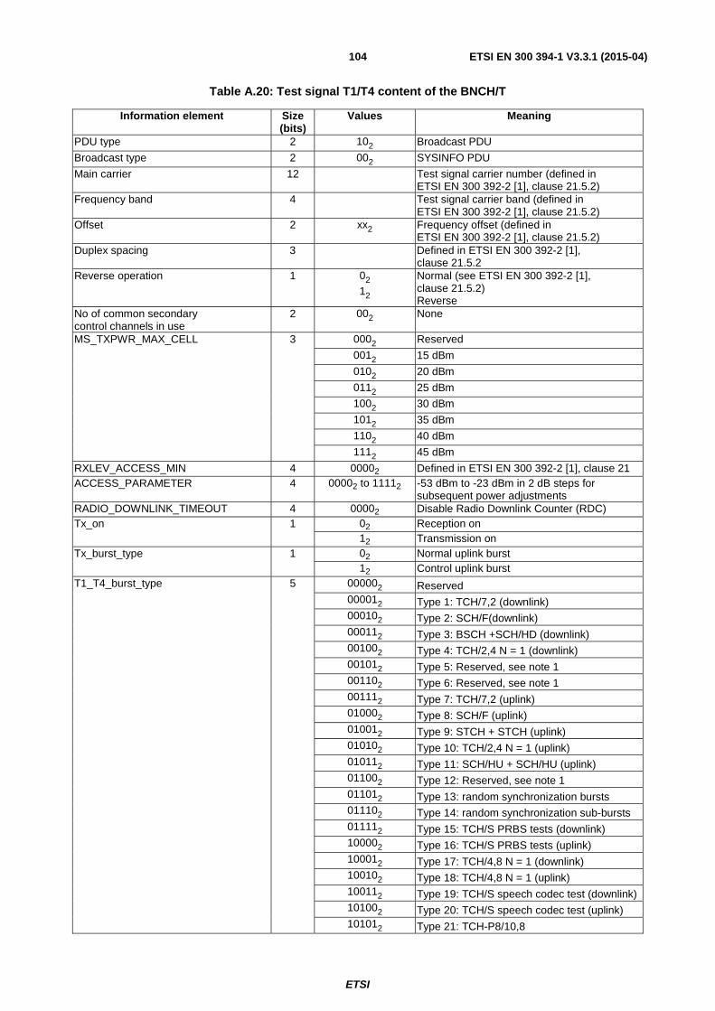
ETSI
ETSI EN 300 394-1 V3.3.1 (2015-04)104
Table A.20: Test signal T1/T4 content of the BNCH/T
Information element Size (bits)
Values Meaning
PDU type 2 102 Broadcast PDU
Broadcast type 2 002 SYSINFO PDU
Main carrier 12 Test signal carrier number (defined in ETSI EN 300 392-2 [1], clause 21.5.2)
Frequency band 4 Test signal carrier band (defined in ETSI EN 300 392-2 [1], clause 21.5.2)
Offset 2 xx2 Frequency offset (defined in ETSI EN 300 392-2 [1], clause 21.5.2)
Duplex spacing 3 Defined in ETSI EN 300 392-2 [1], clause 21.5.2
Reverse operation 1 02 12
Normal (see ETSI EN 300 392-2 [1], clause 21.5.2) Reverse
No of common secondary control channels in use
2 002 None
MS_TXPWR_MAX_CELL 3 0002 Reserved
0012 15 dBm
0102 20 dBm
0112 25 dBm
1002 30 dBm
1012 35 dBm
1102 40 dBm
1112 45 dBm
RXLEV_ACCESS_MIN 4 00002 Defined in ETSI EN 300 392-2 [1], clause 21 ACCESS_PARAMETER 4 00002 to 11112 -53 dBm to -23 dBm in 2 dB steps for
subsequent power adjustments RADIO_DOWNLINK_TIMEOUT 4 00002 Disable Radio Downlink Counter (RDC) Tx_on 1 02 Reception on
12 Transmission on Tx_burst_type 1 02 Normal uplink burst
12 Control uplink burst T1_T4_burst_type 5 000002 Reserved
000012 Type 1: TCH/7,2 (downlink) 000102 Type 2: SCH/F(downlink) 000112 Type 3: BSCH +SCH/HD (downlink) 001002 Type 4: TCH/2,4 N = 1 (downlink) 001012 Type 5: Reserved, see note 1 001102 Type 6: Reserved, see note 1 001112 Type 7: TCH/7,2 (uplink) 010002 Type 8: SCH/F (uplink) 010012 Type 9: STCH + STCH (uplink) 010102 Type 10: TCH/2,4 N = 1 (uplink) 010112 Type 11: SCH/HU + SCH/HU (uplink) 011002 Type 12: Reserved, see note 1 011012 Type 13: random synchronization bursts 011102 Type 14: random synchronization sub-bursts 011112 Type 15: TCH/S PRBS tests (downlink) 100002 Type 16: TCH/S PRBS tests (uplink) 100012 Type 17: TCH/4,8 N = 1 (downlink) 100102 Type 18: TCH/4,8 N = 1 (uplink) 100112 Type 19: TCH/S speech codec test (downlink) 101002 Type 20: TCH/S speech codec test (uplink) 101012 Type 21: TCH-P8/10,8
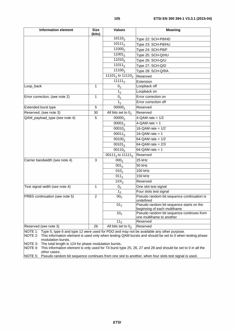
ETSI
ETSI EN 300 394-1 V3.3.1 (2015-04)105
Information element Size (bits)
Values Meaning
101102 Type 22: SCH-P8/HD 101112 Type 23: SCH-P8/HU 110002 Type 24: SCH-P8/F 110012 Type 25: SCH-Q/HU 110102 Type 26: SCH-Q/U 110112 Type 27: SCH-Q/D 111002 Type 28: SCH-Q/RA
111012 to 111102 Reserved 111112 Extension
Loop_back 1 02 Loopback off
12 Loopback on
Error correction, (see note 2) 1 02 Error correction on
12 Error correction off
Extended burst type 5 000002 Reserved
Reserved, (see note 3) 30 All bits set to 02 Reserved
QAM_payload_type (see note 4) 5 000002 4-QAM rate = 1/2
000012 4-QAM rate = 1
000102 16-QAM rate = 1/2
000112 16-QAM rate = 1
001002 64-QAM rate = 1/2
001012 64-QAM rate = 2/3
001102 64-QAM rate = 1
001112 to 111112 Reserved
Carrier bandwidth (see note 4) 3 0002 25 kHz
0012 50 kHz
0102 100 kHz
0112 150 kHz
1XX2 Reserved
Test signal width (see note 4) 1 02 One slot test signal 12 Four slots test signal
PRBS continuation (see note 5) 2 002 Pseudo random bit sequence continuation is undefined
012 Pseudo random bit sequence starts on the beginning of each multiframe
102 Pseudo random bit sequence continues from one multiframe to another
112 Reserved Reserved (see note 3) 26 All bits set to 02 Reserved
NOTE 1: Type 5, type 6 and type 12 were used for PDO and may not be available any other purpose. NOTE 2: This information element is used only when testing QAM bursts and should be set to 0 when testing phase
modulation bursts. NOTE 3: The total length is 124 for phase modulation bursts. NOTE 4: This information element is only used for T4 burst type 25, 26, 27 and 28 and should be set to 0 in all the
other cases. NOTE 5: Pseudo random bit sequence continues from one slot to another, when four slots test signal is used.
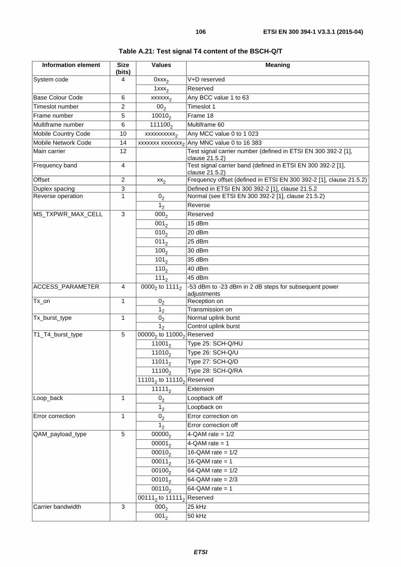
ETSI
ETSI EN 300 394-1 V3.3.1 (2015-04)106
Table A.21: Test signal T4 content of the BSCH-Q/T
Information element Size (bits)
Values Meaning
System code 4 0xxx2 V+D reserved
1xxx2 Reserved
Base Colour Code 6 xxxxxx2 Any BCC value 1 to 63
Timeslot number 2 002 Timeslot 1
Frame number 5 100102 Frame 18
Multiframe number 6 1111002 Multiframe 60
Mobile Country Code 10 xxxxxxxxxx2 Any MCC value 0 to 1 023
Mobile Network Code 14 xxxxxxx xxxxxxx2 Any MNC value 0 to 16 383 Main carrier 12 Test signal carrier number (defined in ETSI EN 300 392-2 [1],
clause 21.5.2) Frequency band 4 Test signal carrier band (defined in ETSI EN 300 392-2 [1],
clause 21.5.2) Offset 2 xx2 Frequency offset (defined in ETSI EN 300 392-2 [1], clause 21.5.2)
Duplex spacing 3 Defined in ETSI EN 300 392-2 [1], clause 21.5.2 Reverse operation 1 02 Normal (see ETSI EN 300 392-2 [1], clause 21.5.2)
12 Reverse
MS_TXPWR_MAX_CELL 3 0002 Reserved
0012 15 dBm
0102 20 dBm
0112 25 dBm
1002 30 dBm
1012 35 dBm
1102 40 dBm
1112 45 dBm
ACCESS_PARAMETER 4 00002 to 11112 -53 dBm to -23 dBm in 2 dB steps for subsequent power adjustments
Tx_on 1 02 Reception on 12 Transmission on
Tx_burst_type 1 02 Normal uplink burst 12 Control uplink burst
T1_T4_burst_type 5 000002 to 110002 Reserved
110012 Type 25: SCH-Q/HU
110102 Type 26: SCH-Q/U
110112 Type 27: SCH-Q/D
111002 Type 28: SCH-Q/RA
111012 to 111102 Reserved
111112 Extension
Loop_back 1 02 Loopback off
12 Loopback on
Error correction 1 02 Error correction on
12 Error correction off
QAM_payload_type 5 000002 4-QAM rate = 1/2
000012 4-QAM rate = 1
000102 16-QAM rate = 1/2
000112 16-QAM rate = 1
001002 64-QAM rate = 1/2
001012 64-QAM rate = 2/3
001102 64-QAM rate = 1
001112 to 111112 Reserved
Carrier bandwidth 3 0002 25 kHz
0012 50 kHz
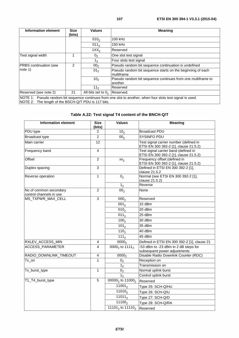
ETSI
ETSI EN 300 394-1 V3.3.1 (2015-04)107
Information element Size (bits)
Values Meaning
0102 100 kHz
0112 150 kHz
1XX2 Reserved
Test signal width 1 02 One slot test signal 12 Four slots test signal
PRBS continuation (see note 1)
2 002 Pseudo random bit sequence continuation is undefined 012 Pseudo random bit sequence starts on the beginning of each
multiframe 102 Pseudo random bit sequence continues from one multiframe to
another 112 Reserved
Reserved (see note 2) 21 All bits set to 02 Reserved.
NOTE 1: Pseudo random bit sequence continues from one slot to another, when four slots test signal is used. NOTE 2: The length of the BSCH-Q/T PDU is 117 bits.
Table A.22: Test signal T4 content of the BNCH-Q/T
Information element Size (bits)
Values Meaning
PDU type 2 102 Broadcast PDU
Broadcast type 2 002 SYSINFO PDU
Main carrier 12 Test signal carrier number (defined in ETSI EN 300 392-2 [1], clause 21.5.2)
Frequency band 4 Test signal carrier band (defined in ETSI EN 300 392-2 [1], clause 21.5.2)
Offset 2 xx2 Frequency offset (defined in ETSI EN 300 392-2 [1], clause 21.5.2)
Duplex spacing 3 Defined in ETSI EN 300 392-2 [1], clause 21.5.2
Reverse operation 1 02 Normal (see ETSI EN 300 392-2 [1], clause 21.5.2)
12 Reverse
No of common secondary control channels in use
2 002 None
MS_TXPWR_MAX_CELL 3 0002 Reserved
0012 15 dBm
0102 20 dBm
0112 25 dBm
1002 30 dBm
1012 35 dBm
1102 40 dBm
1112 45 dBm
RXLEV_ACCESS_MIN 4 00002 Defined in ETSI EN 300 392-2 [1], clause 21 ACCESS_PARAMETER 4 00002 to 11112 -53 dBm to -23 dBm in 2 dB steps for
subsequent power adjustments RADIO_DOWNLINK_TIMEOUT 4 00002 Disable Radio Downlink Counter (RDC) Tx_on 1 02 Reception on
12 Transmission on Tx_burst_type 1 02 Normal uplink burst
12 Control uplink burst T1_T4_burst_type 5 000002 to 110002 Reserved
110012 Type 25: SCH-Q/HU 110102 Type 26: SCH-Q/U 110112 Type 27: SCH-Q/D 111002 Type 28: SCH-Q/RA
111012 to 111102 Reserved
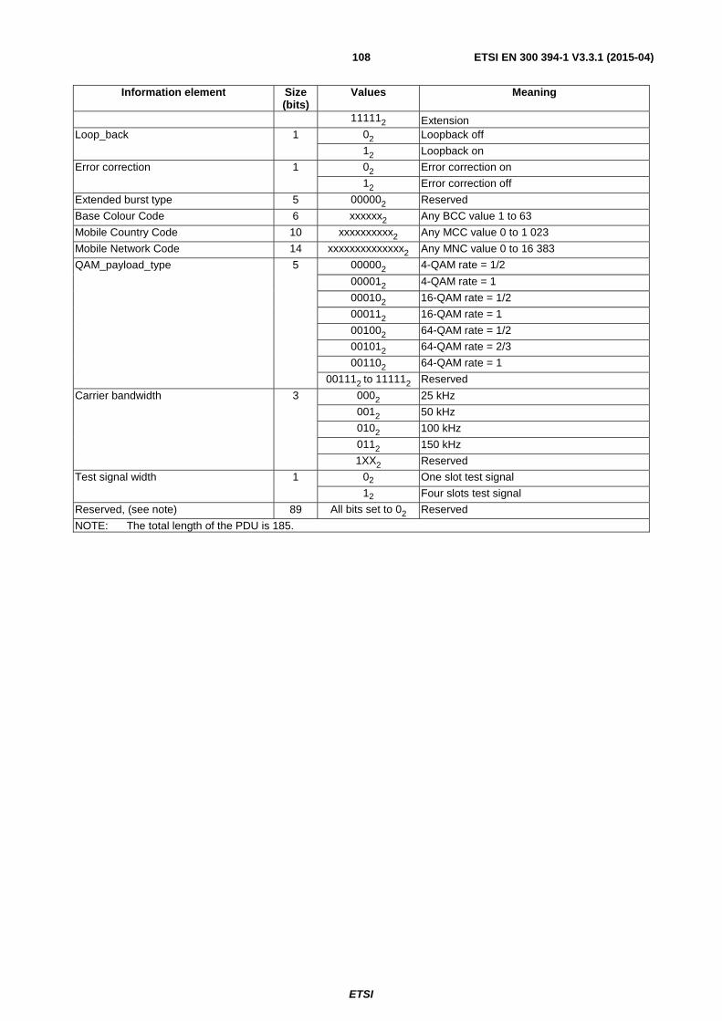
ETSI
ETSI EN 300 394-1 V3.3.1 (2015-04)108
Information element Size (bits)
Values Meaning
111112 Extension Loop_back 1 02 Loopback off
12 Loopback on
Error correction 1 02 Error correction on
12 Error correction off
Extended burst type 5 000002 Reserved
Base Colour Code 6 xxxxxx2 Any BCC value 1 to 63
Mobile Country Code 10 xxxxxxxxxx2 Any MCC value 0 to 1 023
Mobile Network Code 14 xxxxxxxxxxxxxx2 Any MNC value 0 to 16 383
QAM_payload_type 5 000002 4-QAM rate = 1/2
000012 4-QAM rate = 1
000102 16-QAM rate = 1/2
000112 16-QAM rate = 1
001002 64-QAM rate = 1/2
001012 64-QAM rate = 2/3
001102 64-QAM rate = 1
001112 to 111112 Reserved
Carrier bandwidth 3 0002 25 kHz
0012 50 kHz
0102 100 kHz
0112 150 kHz
1XX2 Reserved
Test signal width 1 02 One slot test signal
12 Four slots test signal
Reserved, (see note) 89 All bits set to 02 Reserved
NOTE: The total length of the PDU is 185.
ETSI
ETSI EN 300 394-1 V3.3.1 (2015-04)109
Annex B (normative): Radio test system functions
B.1 Test transmitter and receiver
B.1.1 General The task of the test transmitter/receiver is to simulate either TETRA base station or mobile station functions required while performing the Radio Conformance Testing procedures on the TETRA equipment according to the clauses 8 to 10. These tasks include:
• supporting all the logical channels defined in TETRA;
• supporting the full range of transmit and receive frequencies of TETRA according to ETSI EN 300 392-2 [1], clause 6;
• supplying appropriate signals, see clause B.1.5;
• delaying the transmitted bursts in steps of less than or equal to 125/9 µs, whenever required;
• measuring the nominal Tx power from the DUT in the range from +8 dBm to +48 dBm;
• activating and de-activating specific test modes in the MS, whenever required (optional feature).
B.1.2 Sampling system
B.1.2.1 General
The task of the sampling system, a subsystem of the test receiver, is to acquire a sampled version of a wanted TETRA modulated radio signal or an unwanted emission through the TETRA filter, refer to clause B.1.2.2. The acquired complex samples (I-Q base band representation) are used for modulation accuracy and power measurements.
A sampling rate of at least 4 samples per symbol duration (and per sub-carrier for QAM) is sufficient. The receive frequency of the sampling system shall be adjustable to the nominal equipment transmit frequencies with an uncertainty of ±0,02 ppm (±0,01 ppm for frequencies above 520 MHz). Prior to sampling, frequency down conversion from RF to IF and appropriate IF filtering may take place.
The sampling system shall meet the requirements defined in the clauses B.1.2.2 to B.1.2.4.
B.1.2.2 TETRA filter
The TETRA filter is the receive filter of the sampling system, defined in clauses 5.6 and 5.7 of ETSI EN 300 392-2 [1] as a square root raised cosine filter with a roll-off factor of 0,35 and a symbol duration of 500/9 μs, and additionally the requirements defined in clauses B.1.2.3 to B.1.2.5 shall be met for the sampling system. The TETRA filter shall have a minimum length of 30 symbols.
For QAM power measurements the filter is defined in ETSI EN 300 392-2 [1], clause 5.16.
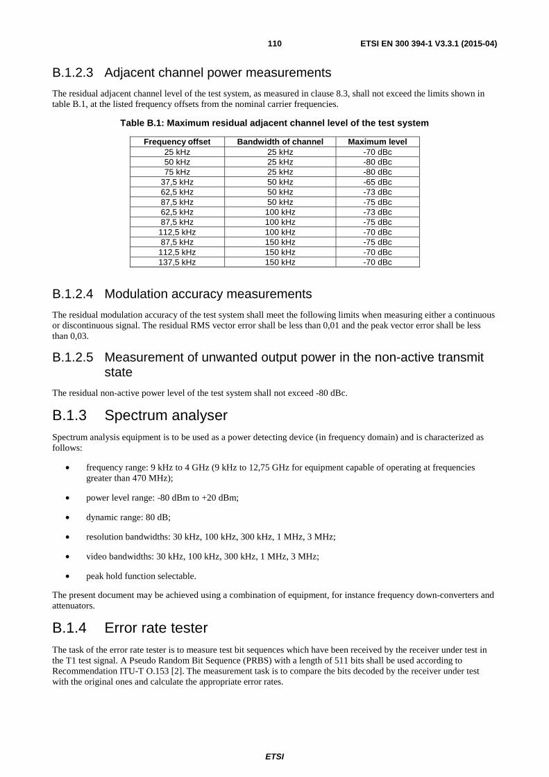
ETSI
ETSI EN 300 394-1 V3.3.1 (2015-04)110
B.1.2.3 Adjacent channel power measurements
The residual adjacent channel level of the test system, as measured in clause 8.3, shall not exceed the limits shown in table B.1, at the listed frequency offsets from the nominal carrier frequencies.
Table B.1: Maximum residual adjacent channel level of the test system
Frequency offset Bandwidth of channel Maximum level 25 kHz 25 kHz -70 dBc 50 kHz 25 kHz -80 dBc 75 kHz 25 kHz -80 dBc
37,5 kHz 50 kHz -65 dBc 62,5 kHz 50 kHz -73 dBc 87,5 kHz 50 kHz -75 dBc 62,5 kHz 100 kHz -73 dBc 87,5 kHz 100 kHz -75 dBc
112,5 kHz 100 kHz -70 dBc 87,5 kHz 150 kHz -75 dBc
112,5 kHz 150 kHz -70 dBc 137,5 kHz 150 kHz -70 dBc
B.1.2.4 Modulation accuracy measurements
The residual modulation accuracy of the test system shall meet the following limits when measuring either a continuous or discontinuous signal. The residual RMS vector error shall be less than 0,01 and the peak vector error shall be less than 0,03.
B.1.2.5 Measurement of unwanted output power in the non-active transmit state
The residual non-active power level of the test system shall not exceed -80 dBc.
B.1.3 Spectrum analyser Spectrum analysis equipment is to be used as a power detecting device (in frequency domain) and is characterized as follows:
• frequency range: 9 kHz to 4 GHz (9 kHz to 12,75 GHz for equipment capable of operating at frequencies greater than 470 MHz);
• power level range: -80 dBm to +20 dBm;
• dynamic range: 80 dB;
• resolution bandwidths: 30 kHz, 100 kHz, 300 kHz, 1 MHz, 3 MHz;
• video bandwidths: 30 kHz, 100 kHz, 300 kHz, 1 MHz, 3 MHz;
• peak hold function selectable.
The present document may be achieved using a combination of equipment, for instance frequency down-converters and attenuators.
B.1.4 Error rate tester The task of the error rate tester is to measure test bit sequences which have been received by the receiver under test in the T1 test signal. A Pseudo Random Bit Sequence (PRBS) with a length of 511 bits shall be used according to Recommendation ITU-T O.153 [2]. The measurement task is to compare the bits decoded by the receiver under test with the original ones and calculate the appropriate error rates.
ETSI
ETSI EN 300 394-1 V3.3.1 (2015-04)111
B.1.5 Test signal requirements
B.1.5.1 On channel test signal T1
Modulation: TETRA π/4-DQPSK or π/8-D8PSK Modulated (see test signal T1 in clause 5.3). The RMS vector error and the peak vector error in any burst as defined in ETSI EN 300 392-2 [1], clause 6 shall be less than 0,03 and 0,1, respectively. These errors shall be measured in a TETRA filter defined in clause B.1.2.2.
Frequency range: TETRA MS and BS receive frequencies.
Uncertainty of frequency: ±0,02 ppm (±0,01 ppm for frequencies above 520 MHz).
Power level range: -115 dBm to -20 dBm, adjustable in steps of 0,2 dB or less.
Uncertainty of power level: See clause 11.
B.1.5.2 Interfering test signal T2
B.1.5.2.1 Phase Modulated
Modulation: TETRA π/4-DQPSK Modulated (see phase modulated test signal T2 in clause 5.3). The RMS vector error and the peak vector error in any burst as defined in ETSI EN 300 392-2 [1], clause 6 shall be less than 0,03 and 0,1, respectively. These errors shall be measured in a TETRA filter defined in clause B.1.2.2.
Frequency range: TETRA MS and BS receive frequencies.
Uncertainty of frequency: ±0,2 ppm (±0,1 ppm for frequencies above 520 MHz).
Power level range: -110 dBm to -50 dBm (after combiner), adjustable in steps of 1 dB or less.
Uncertainty of power level: See clause 11.
Adjacent channel power: The adjacent channel power of phase modulated test signal T2 shall not exceed -70 dBc at 25 kHz offset from the nominal carrier frequency, measured in a TETRA filter defined in clause B.1.2.2. This limit applies to the T2 Test signal under static propagation conditions only.
B.1.5.2.2 QAM Modulated
Modulation: TETRA QAM Modulated (see QAM modulated test signal T2 in clause 5.3). The RMS vector error in any burst as defined in ETSI EN 300 392-2 [1], clause 6 shall be less than 0,02.
Frequency range: TETRA MS and BS receive frequencies.
Uncertainty of frequency: ±0,02 ppm (±0,01 ppm for frequencies above 520 MHz).
Power level range: -110 dBm to -50 dBm (after combiner), adjustable in steps of 1 dB or less.
Uncertainty of power level: See clause 11.
B.1.5.3 Interfering test signal T3
Modulation: T3 is an unmodulated RF signal (see test signal T3 in clause 5.3).
Frequency range: 10 MHz to 4 GHz.
Uncertainty of frequency: ±0,2 ppm (±0,1 ppm for frequencies above 520 MHz).
Power level range: -60 dBm to -25 dBm (after combiner), adjustable in steps of 1 dB or less. Power levels up to 16 dBm are required in the MS transmit band; for transmitter intermodulation attenuation measurement only.
ETSI
ETSI EN 300 394-1 V3.3.1 (2015-04)112
Uncertainty of power level: See clause 11.
Noise: See clause 11.
B.1.5.4 On channel test signal T4
Modulation: TETRA QAM (see test signal T4 in clause 5.3). The RMS vector error in any burst as defined in ETSI EN 300 392-2 [1], clause 6 shall be less than 0,02. For synchronization during MS testing, frame 18 uses phase modulation. See clause B.1.5.1.
Frequency range: TETRA MS and BS receive frequencies.
Uncertainty of frequency: ±0,02 ppm (±0,01 ppm for frequencies above 520 MHz).
Power level range: -115 dBm to -20 dBm, adjustable in steps of 0,2 dB or less.
Uncertainty of power level: See clause 11.
B.1.6 Propagation simulators The task of the propagation simulators is to take into account the effect of the propagation conditions, as described in ETSI EN 300 392-2 [1], clause 6, while testing the receiver performance. The propagation simulators may be either internal or external to the T1 and T2 signal generators. The characteristics of the propagation simulator shall be as follows:
• uncertainty of relative path delay of the fading profile: ±100 ns;
• uncertainty of relative amplitude level of the fading profile: ±0,5 dB;
• the fading profile of all the fading paths shall be uncorrelated.
B.1.7 Timing measurement unit The timing measurement unit is a time interval counter within the test system. It compares the timing (training sequence) of bursts received by the test receiver with the internal timing reference of the test system. The bursts (training sequences) transmitted by the test transmitter shall be synchronized to this internal timing reference.
B.1.8 Passive test system components The task of the passive components is to establish the appropriate interconnection of the test system and the equipment under test. The required composition and characteristics of the passive components depend on the overall implementation of the test system and are not to be defined in the present document. However, the following components may be useful herein: RF combiner, power splitter, isolating device, RF attenuators, connecting cables, mixers, filters and switches.
B.1.9 Test system controller The test system controller co-ordinates the test system functions via an appropriate interface. It may also perform the calculations required by the test procedures and present the final test results whenever appropriate.
ETSI
ETSI EN 300 394-1 V3.3.1 (2015-04)113
Annex C (normative): TETRA Test Connector Interface (TTCI) Annex C defines a TETRA Test Connector Interface for use between TETRA MS/BS equipment and TETRA test equipment.
One of the facilities that has to be provided by the applicant, when submitting equipment for type testing, is a test connector, which provides decoded data output for all uplink logical channels in the case of Base Station (BS) and downlink logical channels in the case of Mobile Station (MS) to be tested.
The TETRA Test Connector Interface (TTCI) is a communication link between the test equipment and the mobile station and base station by which it is possible to automatically register the status, indications and performance of the mobile station.
C.1 General Clause 4.1.1 requires the Mobile Station (MS) and Base Station (BS) only to send decoded data to the test equipment. The TETRA Test Connector Interface (TTCI) is mainly defined as a one-way protocol from the MS/BS to the test equipment, with an option for bi-directional operation. Messages from the test equipment to the MS/BS can be ignored by the MS/BS.
The definition of the TTCI is divided into three different layers. On layer 1 the use of a 25-pole socket with standard electrical characteristics for serial communication is defined. On layer 2, an extremely simple frame oriented protocol is defined. On layer 3, messages for decoded data are defined. Each layer is defined independently of the surrounding layers.
C.2 Formal aspects a) The TTCI is optional for the MS/BS.
b) The TTCI is mandatory for the test equipment.
c) If the TTCI is to be used in conformance testing of an MS/BS, it shall be possible to connect the test equipment to the test connector on the MS/BS, or to an adapter connected to the same MS/BS. If an adapter is to be used, it shall be provided by the manufacturer.
d) If the MS/BS fulfils the requirements performed with the use of a TTCI, the MS/BS is regarded as having passed the test.
e) If the MS/BS is rejected in a test performed with TTCI, the test shall be repeated if possible on the same TETRA equipment with the device carrying the TTCI to the MS/BS removed. The MS/BS shall be regarded as fulfilling the requirements, if it then passes the test.
f) When using the TTCI, the MS / BS does not necessarily conform to the RF requirements. Therefore, tests concerning Rx and Tx parameters on MS / BS with cabinet radiation tests for all types of MS / BS will never be performed with the use of the TTCI.
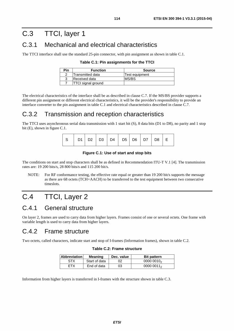
ETSI
ETSI EN 300 394-1 V3.3.1 (2015-04)114
C.3 TTCI, layer 1
C.3.1 Mechanical and electrical characteristics The TTCI interface shall use the standard 25-pin connector, with pin assignment as shown in table C.1.
Table C.1: Pin assignments for the TTCI
Pin Function Source 2 Transmitted data Test equipment 3 Received data MS/BS 7 TTCI signal ground
The electrical characteristics of the interface shall be as described in clause C.7. If the MS/BS provider supports a different pin assignment or different electrical characteristics, it will be the provider's responsibility to provide an interface converter to the pin assignment in table C.1 and electrical characteristics described in clause C.7.
C.3.2 Transmission and reception characteristics The TTCI uses asynchronous serial data transmission with 1 start bit (S), 8 data bits (D1 to D8), no parity and 1 stop bit (E), shown in figure C.1.
S D1 D2 D3 D4 D5 D6 D7 D8 E
Figure C.1: Use of start and stop bits
The conditions on start and stop characters shall be as defined in Recommendation ITU-T V.1 [4]. The transmission rates are: 19 200 bits/s, 28 800 bits/s and 115 200 bit/s.
NOTE: For RF conformance testing, the effective rate equal or greater than 19 200 bit/s supports the message as there are 68 octets (TCH+AACH) to be transferred to the test equipment between two consecutive timeslots.
C.4 TTCI, Layer 2
C.4.1 General structure On layer 2, frames are used to carry data from higher layers. Frames consist of one or several octets. One frame with variable length is used to carry data from higher layers.
C.4.2 Frame structure Two octets, called characters, indicate start and stop of I-frames (Information frames), shown in table C.2.
Table C.2: Frame structure
Abbreviation Meaning Dec. value Bit pattern STX Start of data 02 0000 00102 ETX End of data 03 0000 00112
Information from higher layers is transferred in I-frames with the structure shown in table C.3.
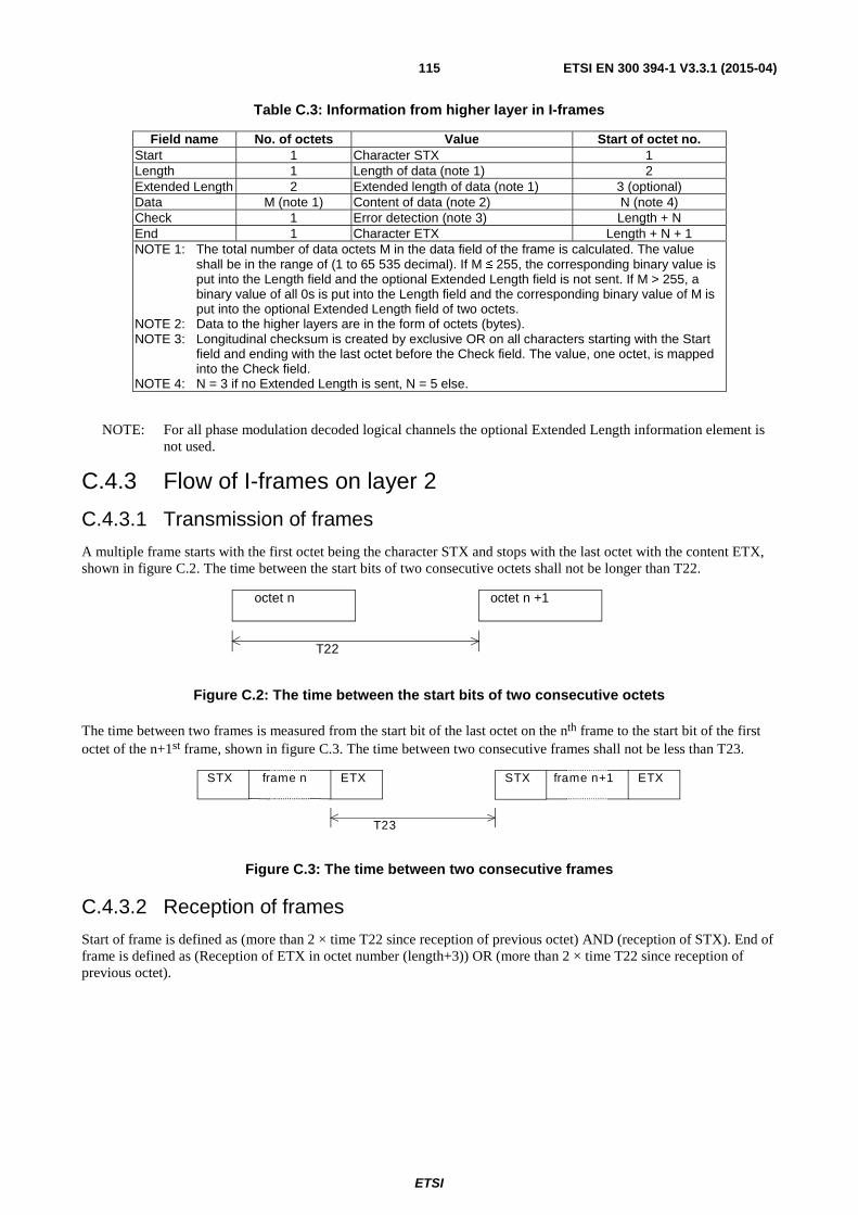
ETSI
ETSI EN 300 394-1 V3.3.1 (2015-04)115
Table C.3: Information from higher layer in I-frames
Field name No. of octets Value Start of octet no. Start 1 Character STX 1 Length 1 Length of data (note 1) 2 Extended Length 2 Extended length of data (note 1) 3 (optional) Data M (note 1) Content of data (note 2) N (note 4) Check 1 Error detection (note 3) Length + N End 1 Character ETX Length + N + 1 NOTE 1: The total number of data octets M in the data field of the frame is calculated. The value
shall be in the range of (1 to 65 535 decimal). If M ≤ 255, the corresponding binary value is put into the Length field and the optional Extended Length field is not sent. If M > 255, a binary value of all 0s is put into the Length field and the corresponding binary value of M is put into the optional Extended Length field of two octets.
NOTE 2: Data to the higher layers are in the form of octets (bytes). NOTE 3: Longitudinal checksum is created by exclusive OR on all characters starting with the Start
field and ending with the last octet before the Check field. The value, one octet, is mapped into the Check field.
NOTE 4: N = 3 if no Extended Length is sent, N = 5 else.
NOTE: For all phase modulation decoded logical channels the optional Extended Length information element is not used.
C.4.3 Flow of I-frames on layer 2
C.4.3.1 Transmission of frames
A multiple frame starts with the first octet being the character STX and stops with the last octet with the content ETX, shown in figure C.2. The time between the start bits of two consecutive octets shall not be longer than T22.
octet n octet n +1
T22
Figure C.2: The time between the start bits of two consecutive octets
The time between two frames is measured from the start bit of the last octet on the nth frame to the start bit of the first octet of the n+1st frame, shown in figure C.3. The time between two consecutive frames shall not be less than T23.
STX ETX frame n STX ETX frame n+1
T23
Figure C.3: The time between two consecutive frames
C.4.3.2 Reception of frames
Start of frame is defined as (more than 2 × time T22 since reception of previous octet) AND (reception of STX). End of frame is defined as (Reception of ETX in octet number (length+3)) OR (more than 2 × time T22 since reception of previous octet).

ETSI
ETSI EN 300 394-1 V3.3.1 (2015-04)116
C.4.3.3 Parameters on layer 2
Layer 2 parameters T22 and T23 are defined in table C.4.
Table C.4: Timer values on layer 2
Bit rate Value of T22 Value of T23 19 200 0,8 ms 1,8 ms 28 800 0,53 ms 1,2 ms
115 200 0,13 ms 0,3 ms
C.5 TTCI, Layer 3
C.5.1 Message structure Messages are used on layer 3. They are defined by Message Identifier (MI) in the range of (0 to 255). The MI is always the first octet of the message. Table C.5 defines the usage of the TTCI Message Identifiers.
Table C.5: Use of message identifiers
MI value Use 0 to 49 Not used in TETRA.
50 to 119 Not used in TETRA. 120 to 179 TETRA General messages. All undefined messages are reserved for TETRA future use. 180 to 209 Not used in TETRA. 210 to 239 Not used in TETRA. 240 to 255 Reserved for Layer 3 error handling. All undefined values reserved for future use.
Table C.6 lists the MI values used in TETRA to send messages from the MS/BS to the test equipment.
Table C.6: Block types
MI value Abbr. Meaning 120 DATO Data output from the MS/BS to the test equipment. Contains the
information received in the logical channel under testing. Preceded by one byte of status to indicate Message Error Flag and the channel type.
121 CONTROL Control commands from the test equipment to BS contains control information about power levels and carrier frequency of BS.
122 CODEC Codec conformance testing. 123 MS sync Optional indicator for successful decoding of transmitted synchronization
bursts. 240 ST indicator Status Detected, in MS or BS.
C.5.2 Definitions of the messages
C.5.2.1 DATO
This message shown in table C.7 is used by the MS and the BS to send the bits extracted from the logical channel under test to the test equipment. In addition, the first octet of the message will contain the Message Error Flag octet. The test equipment shall record those instances when a message error occurred, but the Message Error Flag was not set. This can be used by the test equipment to calculate the MER and PUEM. If the last octet is not full, the rest of the octet is regarded as do not care.
For phase modulation, the AACH decoded information will be available on the test connector following the logical channel(s) information regardless of the channel type tested. In frame 18 the AACH decoded information will also be available following the BSCH and BNCH/T information.
For QAM modulation, the AACH-Q and SICH-Q/D (in case of MS testing) or the SICH-Q/U (in case of BS testing) decoded information will be available on the test connector following the logical channel(s) information regardless of the channel type tested.
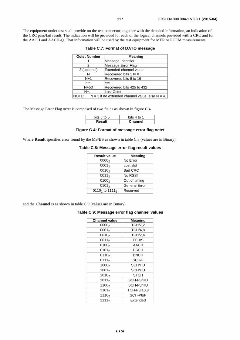
ETSI
ETSI EN 300 394-1 V3.3.1 (2015-04)117
The equipment under test shall provide on the test connector, together with the decoded information, an indication of the CRC pass/fail result. The indication will be provided for each of the logical channels provided with a CRC and for the AACH and AACH-Q. That information will be used by the test equipment for MER or PUEM measurements.
Table C.7: Format of DATO message
Octet Number Meaning 1 Message Identifier 2 Message Error Flag
3 (optional) Extended channel value N Recovered bits 1 to 8
N+1 Recovered bits 9 to 16 etc. etc.
N+53 Recovered bits 425 to 432 N+… Last Octet
NOTE: N = 3 if no extended channel value, else N = 4.
The Message Error Flag octet is composed of two fields as shown in figure C.4.
bits 8 to 5 bits 4 to 1 Result Channel
Figure C.4: Format of message error flag octet
Where Result specifies error found by the MS/BS as shown in table C.8 (values are in Binary).
Table C.8: Message error flag result values
Result value Meaning 00002 No Error 00012 Lost slot 00102 Bad CRC 00112 No RSSI 01002 Out of timing 01012 General Error
01102 to 11112 Reserved
and the Channel is as shown in table C.9 (values are in Binary).
Table C.9: Message error flag channel values
Channel value Meaning 00002 TCH/7,2 00012 TCH/4,8 00102 TCH/2,4 00112 TCH/S 01002 AACH 01012 BSCH 01102 BNCH 01112 SCH/F 10002 SCH/HD 10012 SCH/HU 10102 STCH 10112 SCH-P8/HD 11002 SCH-P8/HU 11012 TCH-P8/10,8 11102 SCH-P8/F 11112 Extended
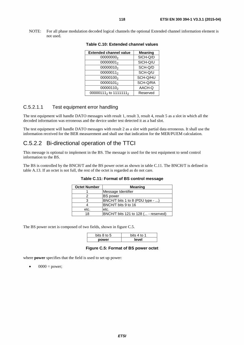
ETSI
ETSI EN 300 394-1 V3.3.1 (2015-04)118
NOTE: For all phase modulation decoded logical channels the optional Extended channel information element is not used.
Table C.10: Extended channel values
Extended channel value Meaning 000000002 SICH-Q/D 000000012 SICH-Q/U 000000102 SCH-Q/D 000000112 SCH-Q/U 000001002 SCH-Q/HU 000001012 SCH-Q/RA 000001102 AACH-Q
000001112 to 11111112 Reserved
C.5.2.1.1 Test equipment error handling
The test equipment will handle DATO messages with result 1, result 3, result 4, result 5 as a slot in which all the decoded information was erroneous and the device under test detected it as a bad slot.
The test equipment will handle DATO messages with result 2 as a slot with partial data erroneous. It shall use the information received for the BER measurement and shall use that indication for the MER/PUEM calculation.
C.5.2.2 Bi-directional operation of the TTCI
This message is optional to implement in the BS. The message is used for the test equipment to send control information to the BS.
The BS is controlled by the BNCH/T and the BS power octet as shown in table C.11. The BNCH/T is defined in table A.13. If an octet is not full, the rest of the octet is regarded as do not care.
Table C.11: Format of BS control message
Octet Number Meaning 1 Message Identifier 2 BS power 3 BNCH/T bits 1 to 8 (PDU type - ...) 4 BNCH/T bits 9 to 16
etc. etc. 18 BNCH/T bits 121 to 128 (... - reserved)
The BS power octet is composed of two fields, shown in figure C.5.
bits 8 to 5 bits 4 to 1 power level
Figure C.5: Format of BS power octet
where power specifies that the field is used to set up power:
• 0000 = power;
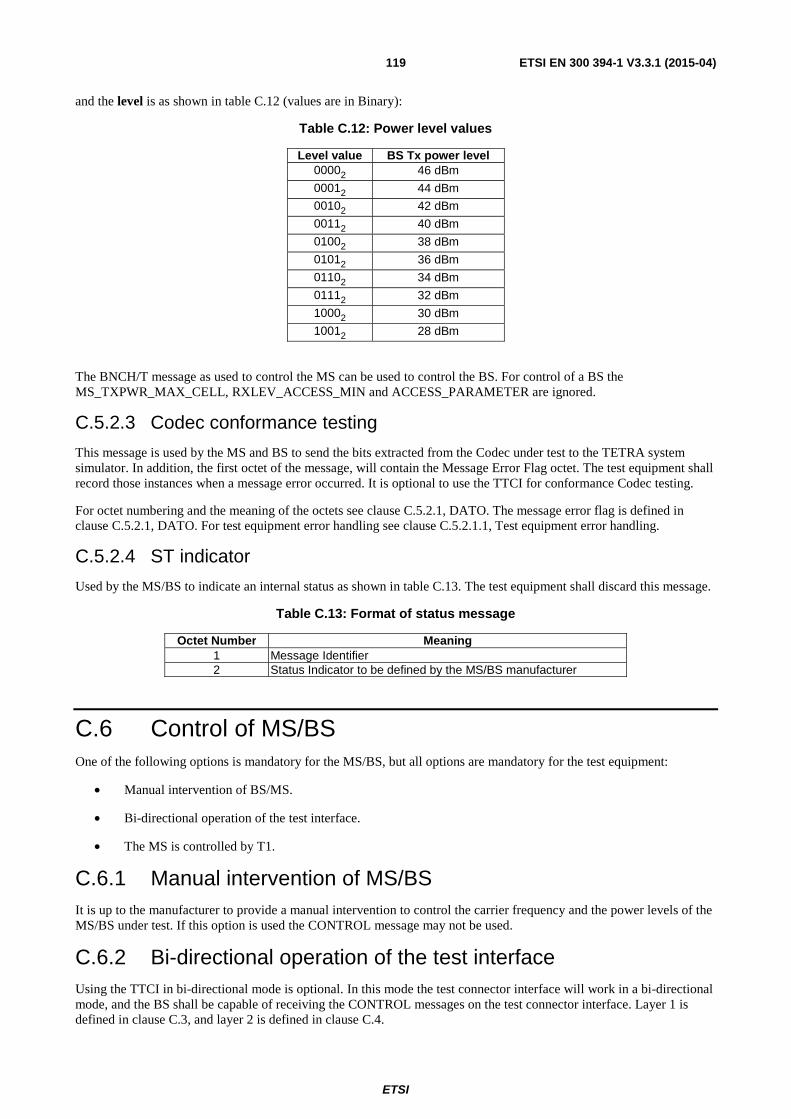
ETSI
ETSI EN 300 394-1 V3.3.1 (2015-04)119
and the level is as shown in table C.12 (values are in Binary):
Table C.12: Power level values
Level value BS Tx power level 00002 46 dBm
00012 44 dBm
00102 42 dBm
00112 40 dBm
01002 38 dBm
01012 36 dBm
01102 34 dBm
01112 32 dBm
10002 30 dBm
10012 28 dBm
The BNCH/T message as used to control the MS can be used to control the BS. For control of a BS the MS_TXPWR_MAX_CELL, RXLEV_ACCESS_MIN and ACCESS_PARAMETER are ignored.
C.5.2.3 Codec conformance testing
This message is used by the MS and BS to send the bits extracted from the Codec under test to the TETRA system simulator. In addition, the first octet of the message, will contain the Message Error Flag octet. The test equipment shall record those instances when a message error occurred. It is optional to use the TTCI for conformance Codec testing.
For octet numbering and the meaning of the octets see clause C.5.2.1, DATO. The message error flag is defined in clause C.5.2.1, DATO. For test equipment error handling see clause C.5.2.1.1, Test equipment error handling.
C.5.2.4 ST indicator
Used by the MS/BS to indicate an internal status as shown in table C.13. The test equipment shall discard this message.
Table C.13: Format of status message
Octet Number Meaning 1 Message Identifier 2 Status Indicator to be defined by the MS/BS manufacturer
C.6 Control of MS/BS One of the following options is mandatory for the MS/BS, but all options are mandatory for the test equipment:
• Manual intervention of BS/MS.
• Bi-directional operation of the test interface.
• The MS is controlled by T1.
C.6.1 Manual intervention of MS/BS It is up to the manufacturer to provide a manual intervention to control the carrier frequency and the power levels of the MS/BS under test. If this option is used the CONTROL message may not be used.
C.6.2 Bi-directional operation of the test interface Using the TTCI in bi-directional mode is optional. In this mode the test connector interface will work in a bi-directional mode, and the BS shall be capable of receiving the CONTROL messages on the test connector interface. Layer 1 is defined in clause C.3, and layer 2 is defined in clause C.4.
ETSI
ETSI EN 300 394-1 V3.3.1 (2015-04)120
C.6.3 MS controlled by T1 In this mode the MS power settings and frequency settings are controlled by the T1 signal on the air-interface.
C.7 Characteristics of the interface It shall be possible to connect the test equipment to the MS/BS or to an adapter connected to the MS/BS. If an adapter is to be used, it shall be provided by the manufacturer of the MS/BS.
C.7.1 Mechanical characteristics of the interface The interface shall use a 25-pin connector, detailed in ISO 2110 [5]; the MS/BS shall use the female part.
The manufacturer may provide this interface on an external test "adapter"; the pin connection shall be as described in table C.1.
C.7.2 Electric characteristics of the interface The state of a signal pin is defined by the voltage (v) between the pin and its associated ground as shown in table C.14.
Table C.14: Electric characteristics of the test interface
Logical state Voltage (v) 0 or "LOW" 1 or "HIGH" undefined forbidden
+5 V < v < +15 V -5 V > v > -15 V -5 V < v < +5 V
v < -15 V, or v > +15 V
C.8 Codec conformance testing using the TTCI This clause specifies a test methodology for using the TTCI for speech codec testing. It is optional to use the TTCI to perform speech codec testing.
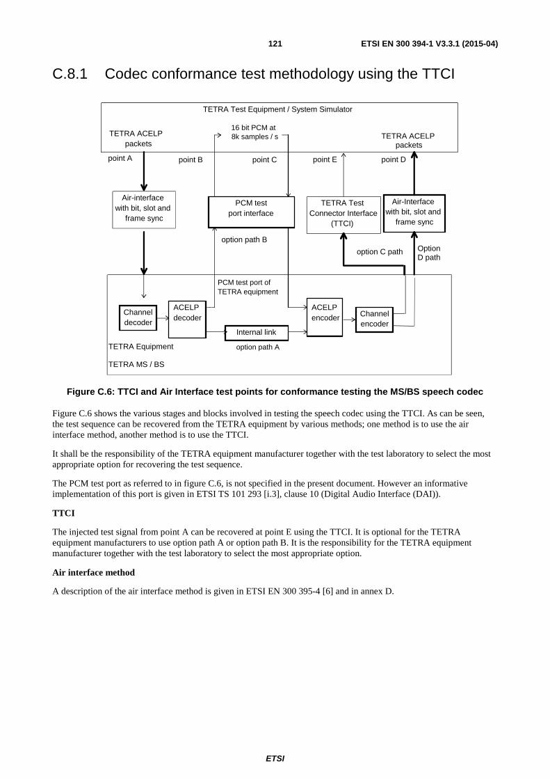
ETSI
ETSI EN 300 394-1 V3.3.1 (2015-04)121
C.8.1 Codec conformance test methodology using the TTCI
TETRA Test Equipment / System Simulator
TETRA Equipment
TETRA MS / BS
Air-interface with bit, slot and
frame sync
Air-Interface with bit, slot and
frame sync
TETRA Test Connector Interface
(TTCI)
point A point E point D
Channel decoder
Channel encoder
ACELP decoder
ACELP encoder
Internal link
TETRA ACELP packets
TETRA ACELPpackets
option C path Option D path
PCM test port interface
point B point C
option path B
option path A
PCM test port of TETRA equipment
16 bit PCM at 8k samples / s
Figure C.6: TTCI and Air Interface test points for conformance testing the MS/BS speech codec
Figure C.6 shows the various stages and blocks involved in testing the speech codec using the TTCI. As can be seen, the test sequence can be recovered from the TETRA equipment by various methods; one method is to use the air interface method, another method is to use the TTCI.
It shall be the responsibility of the TETRA equipment manufacturer together with the test laboratory to select the most appropriate option for recovering the test sequence.
The PCM test port as referred to in figure C.6, is not specified in the present document. However an informative implementation of this port is given in ETSI TS 101 293 [i.3], clause 10 (Digital Audio Interface (DAI)).
TTCI
The injected test signal from point A can be recovered at point E using the TTCI. It is optional for the TETRA equipment manufacturers to use option path A or option path B. It is the responsibility for the TETRA equipment manufacturer together with the test laboratory to select the most appropriate option.
Air interface method
A description of the air interface method is given in ETSI EN 300 395-4 [6] and in annex D.
ETSI
ETSI EN 300 394-1 V3.3.1 (2015-04)122
Annex D (normative): RF test facility using RF loop back Annex D defines a common means of testing RF parameters using an RF loop back facility. It includes definitions of two separate loopback test methods, TETRA Test mode (defined in clauses D.1 to D.6) and T1 test mode (defined in clauses D.7 and D.8) or T4 test mode (defined in clauses D.7 and D.9).
Clauses D.1 to D.6 define a mandatory TETRA Test (TT) protocol entity for use on the air interface between a TETRA MS and a TETRA System Simulator (TSS) to enable the RF loop back to be activated. This method is intended for performing tests on production models of TETRA MS equipment. It assumes the use of a TSS such as a Radio Test Set or similar test equipment which is capable of exchanging air interface signalling messages with the MS under test.
An RF loop back facility enables manufacturing, servicing or conformance testing to be performed without the need for test connectors or leads (except of course for antenna connections) and does not need access to authentication and encryption algorithms. The MS is tested in a state which is similar to its normal operating mode, using standard non-proprietary signalling procedures to set up voice and data calls on traffic channels.
Clauses D.7 and D.8 define a simple T1 test mode RF loop back method for MS and BS equipment which does not involve any signalling protocol to provide a "virtual test connector" for performing the receiver tests specified in clause 9. This simple method is intended for the purpose of performing radio conformance testing using the T1 Test Signal, and it allows radio conformance tests to be performed in isolation on MS and BS equipment which may not implement the higher layers of TETRA protocol. Clauses D.7 and D.9 define a simple T4 test mode RF Loop Back method for MS and BS equipment that is similar to the T1 test mode but uses QAM modulation. The T1 and T4 test mode RF loopback methods are optional. Note that errors could occur due to peak power limitation, so only a physical test connector method is error free. The simple T1 and T4 loopback test modes do not require the test system to support any channel decoding or signalling, and could be implemented in the same test equipment as is used for transmission and modulation measurements. The return channels for T1 loopback are TCH/7,2 (π/4-DQPSK) and TCH-P/10,8 (π/8-D8PSK). For T4 loopback the return channels are SCH-Q/U and SCH-Q/D. It is only necessary for the test equipment to receive and demodulate the burst (already required for modulation measurements) and de-scramble the burst data (which is simply a bit-wise exclusive-OR operation with a known pattern).
At present the applicability of this annex is to TETRA V+D equipment. With the exception of the T4 test mode, it is also applicable to conformance testing of Direct Mode (DMO) equipment tested in accordance with annex F.
For the purposes of this annex the following definitions apply:
• normal operational mode: the state a TETRA MS is in for its normal intended operation in a TETRA system when no test modes have been selected;
• TETRA Test mode: the state a TETRA MS is in when it has been set for TETRA Test mode and is registered to a TETRA System Simulator (TSS) generating a test broadcast channel. In this state the MS shall react to standard message sequences, as it would in normal operational mode, with the exceptions outlined in clause D.3.2.1, and also TETRA Test (TT) protocol messages;
• TETRA loop back mode: the sub-mode of TETRA Test mode when a test call has been set up and RF loopback is active;
• test broadcast channel: the Main Control Channel (MCCH) generated by a TETRA System Simulator using a Mobile Country Code (MCC) of 001 and a Mobile Network Code (MNC) of 001;
• test call: is any call sequence made when in TETRA Test mode. The call procedures possible shall be limited by the capability of the TETRA MS;
• duplex test call: a test call resulting in reception and transmission of a traffic channel in the same TDMA frame on a single timeslot;
• T1 test mode: the special test mode which MS and BS equipment is required to implement when submitted for conformance testing, defined in clause 5.2, using the T1 test signal defined in clause 5.3.2 and either a physical test connector defined in annex C or a virtual test connector (RF loopback) defined in this annex. For the purposes of this annex, T1 test mode includes the simple T1 loopback test mode defined in clauses D.7 and D.8 as a virtual test connector;
ETSI
ETSI EN 300 394-1 V3.3.1 (2015-04)123
• normal T1 test mode: the sub-mode of T1 test mode when RF loopback is not active;
• T1 loopback test mode: the sub-mode of T1 test mode when RF loopback is active;
• T4 test mode: the special test mode that MS and BS equipment is required to implement when submitted for QAM conformance testing, defined in clause 5.2, using the T4 test signal defined in clause 5.3.5 and either a physical test connector defined in annex C or a virtual test connector (RF loopback) defined in this annex. Note that errors could occur due to peak power limitation, so only a physical test connector method is error free. For the purposes of this annex, T4 test mode includes the simple T4 loopback test mode defined in clauses D.7 and D.9 as a virtual test connector;
• normal T4 test mode: the sub-mode of T4 test mode when RF loopback is not active;
• T4 loopback test mode: the sub-mode of T4 test mode when RF loopback is active;
• RF loopback: reception at the air interface of a logical channel which is channel decoded as far as the TMV-SAP (defined in ETSI EN 300 392-2 [1], clause 19) where the output of the channel decoder is transferred to the input of a channel encoder for re-transmission at the air interface. This permits test equipment to measure receiver performance using only the antenna connector and standard non-proprietary signalling. The loopback may alternatively take place at the digital audio interface of a speech codec for the purpose of bit-exact codec conformance testing;
• TETRA Test protocol: the set of air interface messages between the TSS and the MS which are used to control the operation of TETRA Test mode and to select and de-select the TETRA loop back mode. These messages are identified by a unique protocol discriminator in the MLE header;
• TETRA System Simulator: test equipment which is capable of generating a TETRA MCCH and a TETRA Traffic Channel (TCH) in order to simulate a TETRA BS, receiving and decoding control and traffic transmissions from a TETRA MS, and implementing sufficient TETRA protocol such that a TETRA MS under test in TETRA Test mode is able to perform the operations defined in annex D;
• test system: test equipment which is used for radio conformance testing, including a T1 and T4 signal generator, but which does not need to exchange TETRA protocol messages with the MS or BS under test, other than the generation of BSCH/T and BNCH/T information. For the purposes of supporting T1 and T4 loopback test mode, the test system shall be capable of receiving, demodulating and de-scrambling TCH/7,2, TCH-P/10,8, SCH-Q/D and SCH-Q/U data in bursts transmitted by the MS or BS under test, but no other channel decoding capability is required.
D.1 Introduction to the TETRA Test (TT) protocol for RF loop back test
This clause is an introduction to the requirements for the mandatory TETRA Test (TT) protocol for operation over the TETRA Air Interface (AI). This clause does not apply to the T1 test mode.
D.1.1 Outline requirements The TETRA test protocol shall provide the means to activate the RF loop back test facility of TETRA MS equipment, thus using the AI and avoiding the use of special test connectors and their associated protocols. It shall enable the following mandatory test functions to be performed:
• enable the use of test mode in the TETRA MS by means of a known manual selection sequence, and by recognition of a TETRA System Simulator (TSS) generating a valid test broadcast channel;
• confirm that the TETRA MS is in TETRA Test mode by means of an air interface message;
• remove the TETRA Test mode by an air interface message or automatically at power down;
• perform test call set-up and cleardown without the need for the test equipment to have knowledge of the security keys and algorithms (for encryption and authentication);
• set-up a duplex test call using a single timeslot when in test mode, whether or not this is possible in normal operational mode;
ETSI
ETSI EN 300 394-1 V3.3.1 (2015-04)124
• obtain the equipment identity, power class, and receiver class from the MS;
• enable TETRA loop back mode to be selected and de-selected for single-slot duplex traffic channels;
• enable received traffic channels to be decoded as far as the TMV-SAP and then re-encoded and retransmitted over the air interface (RF loop back).
D.1.2 Test modes TETRA test mode shall be activated as described in clause D.3.1; in this mode the TETRA MS behaves as if it where operating in a normal TETRA environment and shall be capable of registering and placing or receiving calls to or from a TETRA System Simulator (TSS) as well as obeying commands from the TSS to change frequency channel, timeslot and MS power level. The MS shall attempt to register with the TSS when the TSS is simulating a Base Station (BS). The TETRA MS shall be able to transmit and receive all logical channels for which it has been configured. However in this mode the MS shall not use the air interface encryption, the MS shall not attempt to challenge the TSS for authentication, and the TSS shall not attempt to challenge the MS for authentication. Certain MM messages (defined in clause D.3.2.1) shall be ignored by the MS. When requested by the TSS, the TETRA MS shall identify itself with its TETRA Equipment Identity (TEI), power class (1, 1L, 2, 2L, 3, 3L, 4, 4L, 5 or 5L), and MS receiver class (A, B, D or E). The MS shall also supply its current TETRA Subscriber Identity (TSI) if available and applicable.
TETRA loop back mode is a sub-mode of TETRA Test mode and is only accessible when TETRA Test mode is active and a single-slot duplex test call is in progress. A TETRA MS capable of only simplex operation in its normal operational mode shall be capable of a duplex test call in TETRA Test mode, although this need not include speech codec or data terminal operations. The TETRA MS shall receive the current downlink traffic channel and after decoding as far as the TMV-SAP, re-encode and return the contents on the current uplink traffic channel, being the same type of channel as that received on the downlink. In the case of TCH/S, loop back with Bad Frame Indication (BFI) may be selected, whereby a recognizable bit pattern is returned in the event that a received and decoded speech frame indicates parity failure.

ETSI
ETSI EN 300 394-1 V3.3.1 (2015-04)125
D.1.3 Switching for loop back test mode Figure D.1 shows the functional requirements for loop back test modes. The actual physical implementation is left open to the manufacturer.
Channel Encoder SPEECH
TCH/S
Speech Encoder (optional)
ADC (optional)
Channel Decoder SPEECH
TCH/S
Speech Decoder (optional)
DAC (optional)
Channel Encoder DATA TCH/7.2 TCH/4.8 TCH/2.4
Terminal or Terminal Adapter (optional)
Channel Encoder Signalling STCH SCH/HU SCH/F
Channel Decoder Signalling STCH SCH/HD SCH/F BSCH BNCH
TETRA Signalling Control
Transmit
RF TX front end/modulator
Receive
RF RX front end/
demodulator
Channel Decoder DATA TCH/7.2 TCH/4.8 TCH/2.4
Mode Switch
normal TETRA test TETRA loop back
Store
DMO only
Store
DMO only
Figure D.1: Functional requirements for TETRA loop back
D.2 TETRA test entity This clause defines the Services offered by the TETRA Test entity for the TETRA layer 3 Air Interface. This clause does not apply to the T1 test mode.
The TETRA Test entity shall provide access to special test procedures (defined in annex D) through a TETRA Test Service Access Point (TT-SAP), and uses the services of the Mobile Link Entity (MLE) through the LTT-SAP. Figure D.2 shows an overview of how the TETRA Test entity fits within the general TETRA protocol stack. During TETRA Test mode, interaction between the TT entity and the Mobility Management (MM) entity may be required in order to restrict the MM operation as defined in clause D.3.2.1.
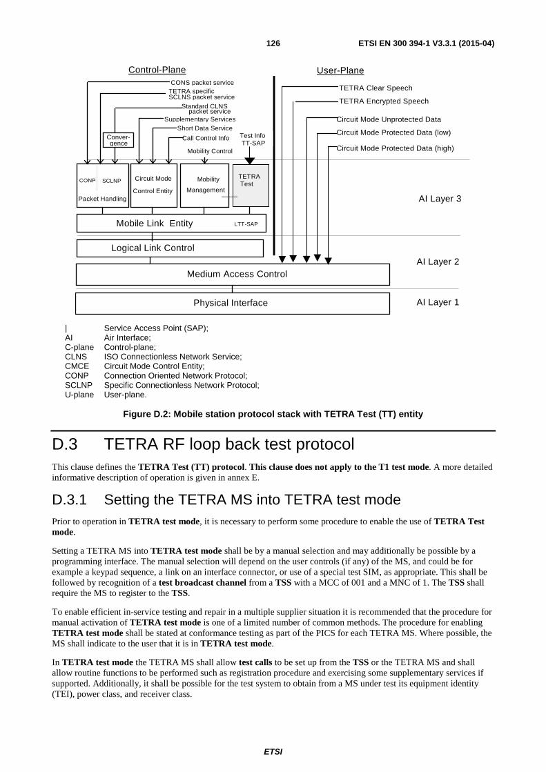
ETSI
ETSI EN 300 394-1 V3.3.1 (2015-04)126
AI Layer 2
AI Layer 1
Mobile Link Entity
Logical Link Control
Medium Access Control
Physical Interface
Circuit Mode
Control Entity Packet Handling
Mobility
Management
TETRA Clear Speech
TETRA Encrypted Speech
Circuit Mode Unprotected Data
Circuit Mode Protected Data (low)
Circuit Mode Protected Data (high)
AI Layer 3
SCLNP
Call Control Info
Short Data Service Supplementary Services
Mobility Control
Control-Plane User-Plane
CONP
CONS packet service
SCLNS packet service TETRA specific
packet service Standard CLNS
Conver- gence
TETRA Test
Test Info TT-SAP
LTT-SAP
| Service Access Point (SAP); AI Air Interface; C-plane Control-plane; CLNS ISO Connectionless Network Service; CMCE Circuit Mode Control Entity; CONP Connection Oriented Network Protocol; SCLNP Specific Connectionless Network Protocol; U-plane User-plane.
Figure D.2: Mobile station protocol stack with TETRA Test (TT) entity
D.3 TETRA RF loop back test protocol This clause defines the TETRA Test (TT) protocol. This clause does not apply to the T1 test mode. A more detailed informative description of operation is given in annex E.
D.3.1 Setting the TETRA MS into TETRA test mode Prior to operation in TETRA test mode, it is necessary to perform some procedure to enable the use of TETRA Test mode.
Setting a TETRA MS into TETRA test mode shall be by a manual selection and may additionally be possible by a programming interface. The manual selection will depend on the user controls (if any) of the MS, and could be for example a keypad sequence, a link on an interface connector, or use of a special test SIM, as appropriate. This shall be followed by recognition of a test broadcast channel from a TSS with a MCC of 001 and a MNC of 1. The TSS shall require the MS to register to the TSS.
To enable efficient in-service testing and repair in a multiple supplier situation it is recommended that the procedure for manual activation of TETRA test mode is one of a limited number of common methods. The procedure for enabling TETRA test mode shall be stated at conformance testing as part of the PICS for each TETRA MS. Where possible, the MS shall indicate to the user that it is in TETRA test mode.
In TETRA test mode the TETRA MS shall allow test calls to be set up from the TSS or the TETRA MS and shall allow routine functions to be performed such as registration procedure and exercising some supplementary services if supported. Additionally, it shall be possible for the test system to obtain from a MS under test its equipment identity (TEI), power class, and receiver class.

ETSI
ETSI EN 300 394-1 V3.3.1 (2015-04)127
With a test call in progress, TETRA loop back mode can be selected which shall configure the TETRA MS to loop back the current traffic channel to the TSS without access to special test connectors. This enables the TSS to measure receiver performance of the MS in terms of Bit Error Rate (BER) and, in the case of TCH/S, Probability of Undetected Erroneous Message (PUEM) and Message Erasure Rate (MER). The TETRA MS shall return received traffic channel data via its air interface thus also allowing RF power, burst profile, frequency and modulation accuracy measurements to be performed on the transmitter of the MS with the content of the scrambled bits of the transmitted bursts being supplied by the TSS.
D.3.2 TETRA test protocol To operate the TETRA test mode over the air interface the TETRA test (TT) Protocol shall be used with the protocol discriminator reserved for test purposes in the Mobile Link Entity (MLE) protocol, defined in ETSI EN 300 392-2 [1], clause 18.5.21. The TETRA test protocol shall use services provided by the MLE at a LTT-SAP. When TETRA test mode is not enabled, the TETRA MS shall ignore all messages with the TETRA Test (TT) protocol discriminator.
The TETRA Test (TT) protocol messages are used to perform the following operations.
D.3.2.1 Confirming that TETRA test mode is set
When the TETRA MS is set into TETRA test mode it shall start a timer T-TEST. This timer is stopped when the TETRA MS is registered with the TSS and a D-TEST MODE CONFIRM COMMAND message is received from the TSS. If a D-TEST MODE CONFIRM COMMAND message is not received by the time T-TEST has expired then the TETRA MS shall exit TETRA Test mode and revert back to its normal operational mode. The time for T-TEST shall be 30 s. This allows time for cell selection and registration to the TSS to be completed before the D-TEST MODE CONFIRM COMMAND message is sent, but ensures that the TETRA MS returns to normal operational mode if TETRA test mode has been inadvertently selected.
A D-TEST MODE CONFIRM COMMAND message requests the TETRA MS to confirm that it has been set to TETRA test mode.
A U-TEST MODE CONFIRM message from the TETRA MS confirms that it is in TETRA test mode (or not). Parameters included with this message shall inform the TSS of the TEI, Power class and Receiver class (A, B, D or E) of the MS.
In TETRA test mode the TETRA MS shall not send an authentication challenge to the TSS, and the TSS shall not send an authentication challenge to the TETRA MS as it may not have its SIM present (if this is an option) or be programmed with its security information. Air encryption shall not be used. The following MM messages (defined in ETSI EN 300 392-2 [1], clause 16 and ETSI EN 300 392-7 [9], clause 4) shall be ignored by the MS whilst in TETRA test mode, and should not be sent by the TSS to the MS whilst it is in TETRA test mode:
• D-ATTACH/DETACH GROUP IDENTITY;
• D-ATTACH/DETACH GROUP IDENTITY ACKNOWLEDGEMENT;
• D-DISABLE;
• D-ENABLE;
• D-AUTHENTICATION DEMAND;
• D-AUTHENTICATION RESPONSE;
• D-AUTHENTICATION RESULT;
• D-OTAR.
The TETRA MS shall return a U-STATUS message with a failure indication if one of the above messages is received whilst in TETRA test mode.
The TETRA MS shall not send the following MM messages whilst in TETRA test mode:
• U-ATTACH/DETACH GROUP IDENTITY;
• U-ATTACH/DETACH GROUP IDENTITY ACKNOWLEDGEMENT;
ETSI
ETSI EN 300 394-1 V3.3.1 (2015-04)128
• U-AUTHENTICATION RESPONSE;
• U-AUTHENTICATION DEMAND;
• U-AUTHENTICATION RESULT;
• U-OTAR.
The TETRA MS whilst in TETRA test mode shall not action the Supplementary Service (SS) procedure Dynamic Group Number Assignment (DGNA) defined in ETSI ETS 300 392-11-22 [10] and ETSI EN 300 392-12-22 [11]. The TETRA MS shall ignore an ASSIGN indication (ETSI EN 300 392-12-22 [11], clause 5.2.1). Where acknowledgement is required it shall send an ASSIGN-ACK response with the result for assignment element (ETSI EN 300 392-12-22 [11], clause 5.2.2) set to rejected for any reason.
When TETRA test mode has been confirmed the TETRA MS shall react to further TETRA Test (TT) protocol commands, as well as normal protocol commands (subject to the restrictions described above).
D.3.2.2 Operating TETRA loop back
To operate TETRA loop back, a test call shall be in an active state.
A D-LOOP COMMAND message requests the TETRA MS to go into TETRA loop back mode. A message parameter indicates whether to indicate errors or not (erased frames) in the case of a speech channel. Currently the present document is limited to single slot traffic channels. The TETRA MS shall ignore the D-LOOP COMMAND message if a test call is not active, or if TETRA loop back mode is already active. To change the loop back type (i.e. to switch between TCH/S with frame erasure and TCH/S without frame erasure) the TSS shall first end the loop back mode which is currently active.
When TETRA loop back is operating the TETRA MS shall be in a single slot duplex mode. It is recommended that the TSS does not attempt to change the traffic channel type or to assign the MS to a different frequency channel or TN during TETRA loop back.
A U-LOOP CONFIRM message from the TETRA MS confirms that it has set TETRA loop back. This message may be sent as unacknowledged data within a layer 2 Basic Link Acknowledge (BL-ACK).
A D-OPEN LOOP COMMAND message from the TSS requests the TETRA MS to end the current TETRA loop back.
A U-OPEN LOOP CONFIRM message from the TETRA MS confirms that it has ended TETRA loop back. This message may be sent as unacknowledged data within a layer 2 Basic Link Acknowledge (BL-ACK).
D.3.2.3 Ending TETRA test mode
TETRA test mode is terminated when the TETRA MS is powered down. It may also be terminated without powering down by some other manual action or over the air interface. On return to normal operational mode the TETRA MS shall behave as if it were just powered up and search for a BS with a valid MCC and MNC.
A D-TEST MODE END COMMAND message requests the TETRA MS to revert to normal operational mode. To reset TETRA test mode shall now, firstly, require the manual setting procedure.
A U-TEST MODE END CONFIRM message from the TETRA MS confirms that it is reverting to normal operational mode.
D.3.3 Bad frame indication If loopback with frame erasure is active, bad frames detected in a speech channel shall be indicated by replacing the type 1-channel bits for recoding/transmission with a value not valid in normal use. This signal shall be 137 bits each set to "1" for each of speech frames A and B.
The speech channel normally carries two speech frames, A and B, which are coded together; in the event that a bad frame is detected, both A and B frames are erased. In the event that frame stealing is indicated during speech channel loopback testing, the MS shall not attempt to decode and return bits for speech frame B. It is recommended that the TSS does not use the STCH during BER/MER tests on any of the traffic channels.
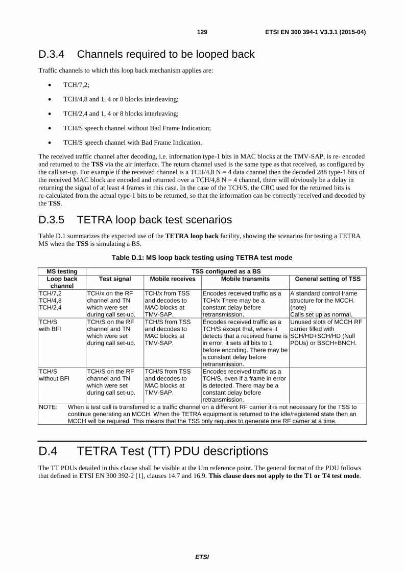
ETSI
ETSI EN 300 394-1 V3.3.1 (2015-04)129
D.3.4 Channels required to be looped back Traffic channels to which this loop back mechanism applies are:
• TCH/7,2;
• TCH/4,8 and 1, 4 or 8 blocks interleaving;
• TCH/2,4 and 1, 4 or 8 blocks interleaving;
• TCH/S speech channel without Bad Frame Indication;
• TCH/S speech channel with Bad Frame Indication.
The received traffic channel after decoding, i.e. information type-1 bits in MAC blocks at the TMV-SAP, is re- encoded and returned to the TSS via the air interface. The return channel used is the same type as that received, as configured by the call set-up. For example if the received channel is a TCH/4,8 N = 4 data channel then the decoded 288 type-1 bits of the received MAC block are encoded and returned over a TCH/4,8 N = 4 channel, there will obviously be a delay in returning the signal of at least 4 frames in this case. In the case of the TCH/S, the CRC used for the returned bits is re-calculated from the actual type-1 bits to be returned, so that the information can be correctly received and decoded by the TSS.
D.3.5 TETRA loop back test scenarios Table D.1 summarizes the expected use of the TETRA loop back facility, showing the scenarios for testing a TETRA MS when the TSS is simulating a BS.
Table D.1: MS loop back testing using TETRA test mode
MS testing TSS configured as a BS Loop back
channel Test signal Mobile receives Mobile transmits General setting of TSS
TCH/7,2 TCH/4,8 TCH/2,4
TCH/x on the RF channel and TN which were set during call set-up.
TCH/x from TSS and decodes to MAC blocks at TMV-SAP.
Encodes received traffic as a TCH/x There may be a constant delay before retransmission.
A standard control frame structure for the MCCH. (note) Calls set up as normal.
TCH/S with BFI
TCH/S on the RF channel and TN which were set during call set-up.
TCH/S from TSS and decodes to MAC blocks at TMV-SAP.
Encodes received traffic as a TCH/S except that, where it detects that a received frame is in error, it sets all bits to 1 before encoding. There may be a constant delay before retransmission.
Unused slots of MCCH RF carrier filled with SCH/HD+SCH/HD (Null PDUs) or BSCH+BNCH.
TCH/S without BFI
TCH/S on the RF channel and TN which were set during call set-up.
TCH/S from TSS and decodes to MAC blocks at TMV-SAP.
Encodes received traffic as a TCH/S, even if a frame in error is detected. There may be a constant delay before retransmission.
NOTE: When a test call is transferred to a traffic channel on a different RF carrier it is not necessary for the TSS to continue generating an MCCH. When the TETRA equipment is returned to the idle/registered state then an MCCH will be required. This means that the TSS only requires to generate one RF carrier at a time.
D.4 TETRA Test (TT) PDU descriptions The TT PDUs detailed in this clause shall be visible at the Um reference point. The general format of the PDU follows that defined in ETSI EN 300 392-2 [1], clauses 14.7 and 16.9. This clause does not apply to the T1 or T4 test mode.
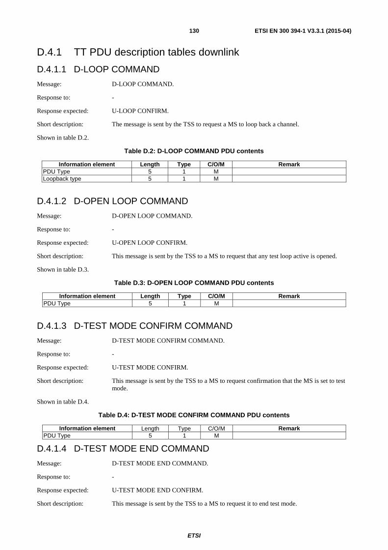
ETSI
ETSI EN 300 394-1 V3.3.1 (2015-04)130
D.4.1 TT PDU description tables downlink
D.4.1.1 D-LOOP COMMAND
Message: D-LOOP COMMAND.
Response to: -
Response expected: U-LOOP CONFIRM.
Short description: The message is sent by the TSS to request a MS to loop back a channel.
Shown in table D.2.
Table D.2: D-LOOP COMMAND PDU contents
Information element Length Type C/O/M Remark PDU Type 5 1 M Loopback type 5 1 M
D.4.1.2 D-OPEN LOOP COMMAND
Message: D-OPEN LOOP COMMAND.
Response to: -
Response expected: U-OPEN LOOP CONFIRM.
Short description: This message is sent by the TSS to a MS to request that any test loop active is opened.
Shown in table D.3.
Table D.3: D-OPEN LOOP COMMAND PDU contents
Information element Length Type C/O/M Remark PDU Type 5 1 M
D.4.1.3 D-TEST MODE CONFIRM COMMAND
Message: D-TEST MODE CONFIRM COMMAND.
Response to: -
Response expected: U-TEST MODE CONFIRM.
Short description: This message is sent by the TSS to a MS to request confirmation that the MS is set to test mode.
Shown in table D.4.
Table D.4: D-TEST MODE CONFIRM COMMAND PDU contents
Information element Length Type C/O/M Remark PDU Type 5 1 M
D.4.1.4 D-TEST MODE END COMMAND
Message: D-TEST MODE END COMMAND.
Response to: -
Response expected: U-TEST MODE END CONFIRM.
Short description: This message is sent by the TSS to a MS to request it to end test mode.
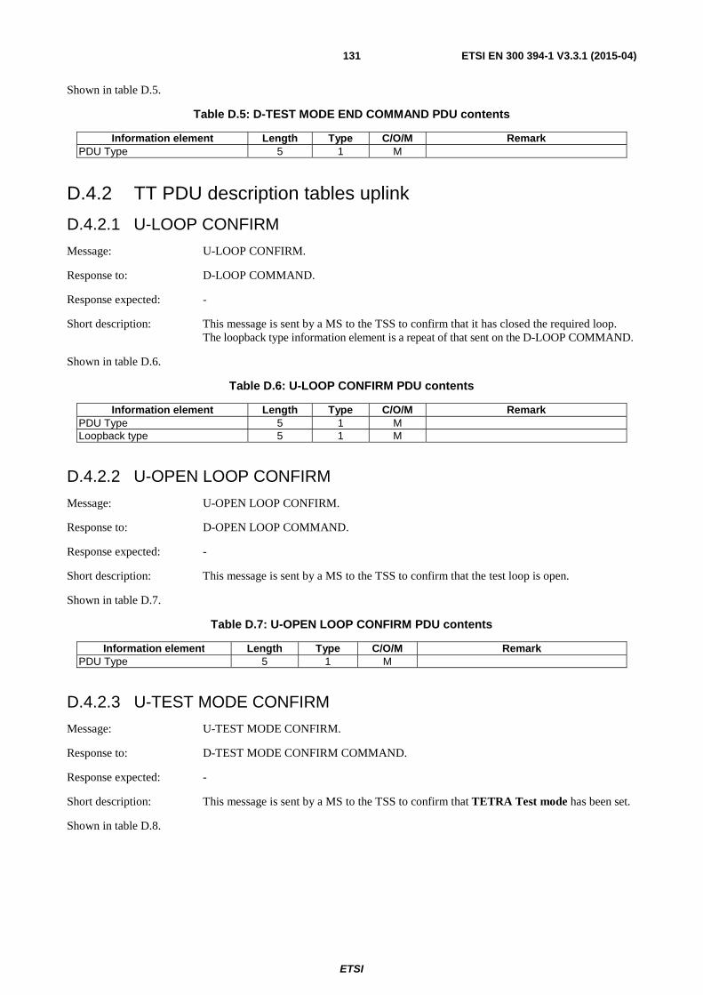
ETSI
ETSI EN 300 394-1 V3.3.1 (2015-04)131
Shown in table D.5.
Table D.5: D-TEST MODE END COMMAND PDU contents
Information element Length Type C/O/M Remark PDU Type 5 1 M
D.4.2 TT PDU description tables uplink
D.4.2.1 U-LOOP CONFIRM
Message: U-LOOP CONFIRM.
Response to: D-LOOP COMMAND.
Response expected: -
Short description: This message is sent by a MS to the TSS to confirm that it has closed the required loop. The loopback type information element is a repeat of that sent on the D-LOOP COMMAND.
Shown in table D.6.
Table D.6: U-LOOP CONFIRM PDU contents
Information element Length Type C/O/M Remark PDU Type 5 1 M Loopback type 5 1 M
D.4.2.2 U-OPEN LOOP CONFIRM
Message: U-OPEN LOOP CONFIRM.
Response to: D-OPEN LOOP COMMAND.
Response expected: -
Short description: This message is sent by a MS to the TSS to confirm that the test loop is open.
Shown in table D.7.
Table D.7: U-OPEN LOOP CONFIRM PDU contents
Information element Length Type C/O/M Remark PDU Type 5 1 M
D.4.2.3 U-TEST MODE CONFIRM
Message: U-TEST MODE CONFIRM.
Response to: D-TEST MODE CONFIRM COMMAND.
Response expected: -
Short description: This message is sent by a MS to the TSS to confirm that TETRA Test mode has been set.
Shown in table D.8.
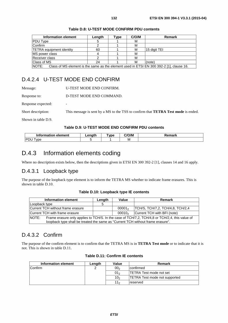
ETSI
ETSI EN 300 394-1 V3.3.1 (2015-04)132
Table D.8: U-TEST MODE CONFIRM PDU contents
Information element Length Type C/O/M Remark PDU Type 5 1 M Confirm 2 1 M TETRA equipment identity 60 1 M 15 digit TEI MS power class 4 1 M Receiver class 2 1 M Class of MS 24 1 M (note) NOTE: Class of MS element is the same as the element used in ETSI EN 300 392-2 [1], clause 16.
D.4.2.4 U-TEST MODE END CONFIRM
Message: U-TEST MODE END CONFIRM.
Response to: D-TEST MODE END COMMAND.
Response expected: -
Short description: This message is sent by a MS to the TSS to confirm that TETRA Test mode is ended.
Shown in table D.9.
Table D.9: U-TEST MODE END CONFIRM PDU contents
Information element Length Type C/O/M Remark PDU Type 5 1 M
D.4.3 Information elements coding Where no description exists below, then the descriptions given in ETSI EN 300 392-2 [1], clauses 14 and 16 apply.
D.4.3.1 Loopback type
The purpose of the loopback type element is to inform the TETRA MS whether to indicate frame erasures. This is shown in table D.10.
Table D.10: Loopback type IE contents
Information element Length Value Remark Loopback type 5 Current TCH without frame erasure 000012 TCH/S, TCH/7,2, TCH/4,8, TCH/2,4 Current TCH with frame erasure 000102 Current TCH with BFI (note) NOTE: Frame erasure only applies to TCH/S. In the case of TCH/7,2, TCH/4,8 or TCH/2,4, this value of
loopback type shall be treated the same as "Current TCH without frame erasure".
D.4.3.2 Confirm
The purpose of the confirm element is to confirm that the TETRA MS is in TETRA Test mode or to indicate that it is not. This is shown in table D.11.
Table D.11: Confirm IE contents
Information element Length Value Remark Confirm 2 002 confirmed
012 TETRA Test mode not set 102 TETRA Test mode not supported 112 reserved
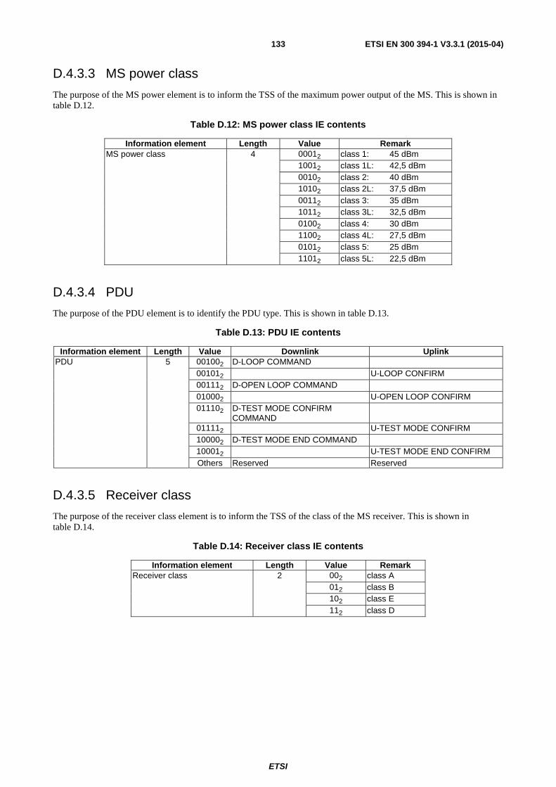
ETSI
ETSI EN 300 394-1 V3.3.1 (2015-04)133
D.4.3.3 MS power class
The purpose of the MS power element is to inform the TSS of the maximum power output of the MS. This is shown in table D.12.
Table D.12: MS power class IE contents
Information element Length Value Remark MS power class 4 00012 class 1: 45 dBm
10012 class 1L: 42,5 dBm 00102 class 2: 40 dBm 10102 class 2L: 37,5 dBm 00112 class 3: 35 dBm 10112 class 3L: 32,5 dBm 01002 class 4: 30 dBm 11002 class 4L: 27,5 dBm 01012 class 5: 25 dBm 11012 class 5L: 22,5 dBm
D.4.3.4 PDU
The purpose of the PDU element is to identify the PDU type. This is shown in table D.13.
Table D.13: PDU IE contents
Information element Length Value Downlink Uplink PDU 5 001002 D-LOOP COMMAND
001012 U-LOOP CONFIRM 001112 D-OPEN LOOP COMMAND 010002 U-OPEN LOOP CONFIRM 011102 D-TEST MODE CONFIRM
COMMAND
011112 U-TEST MODE CONFIRM 100002 D-TEST MODE END COMMAND 100012 U-TEST MODE END CONFIRM Others Reserved Reserved
D.4.3.5 Receiver class
The purpose of the receiver class element is to inform the TSS of the class of the MS receiver. This is shown in table D.14.
Table D.14: Receiver class IE contents
Information element Length Value Remark Receiver class 2 002 class A
012 class B 102 class E 112 class D
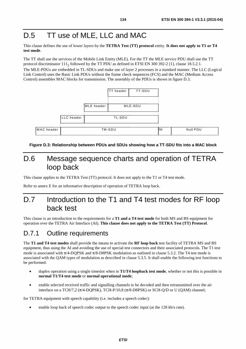
ETSI
ETSI EN 300 394-1 V3.3.1 (2015-04)134
D.5 TT use of MLE, LLC and MAC This clause defines the use of lower layers by the TETRA Test (TT) protocol entity. It does not apply to T1 or T4 test mode.
The TT shall use the services of the Mobile Link Entity (MLE). For the TT the MLE service PDU shall use the TT protocol discriminator 1112 followed by the TT PDU as defined in ETSI EN 300 392-2 [1], clause 18.5.2.1.
The MLE-PDUs are embedded in TL-SDUs and make use of layer 2 processes in a standard manner. The LLC (Logical Link Control) uses the Basic Link PDUs without the frame check sequences (FCS) and the MAC (Medium Access Control) assembles MAC blocks for transmission. The assembly of the PDUs is shown in figure D.3.
TM -SD U M AC header fill N ull PDU
TL-SD U LLC header
M LE header M LE-SD U
TT header TT -SD U
Figure D.3: Relationship between PDUs and SDUs showing how a TT-SDU fits into a MAC block
D.6 Message sequence charts and operation of TETRA loop back
This clause applies to the TETRA Test (TT) protocol. It does not apply to the T1 or T4 test mode.
Refer to annex E for an informative description of operation of TETRA loop back.
D.7 Introduction to the T1 and T4 test modes for RF loop back test
This clause is an introduction to the requirements for a T1 and a T4 test mode for both MS and BS equipment for operation over the TETRA Air Interface (AI). This clause does not apply to the TETRA Test (TT) Protocol.
D.7.1 Outline requirements The T1 and T4 test modes shall provide the means to activate the RF loop back test facility of TETRA MS and BS equipment, thus using the AI and avoiding the use of special test connectors and their associated protocols. The T1 test mode is associated with π/4-DQPSK and π/8-D8PSK modulation as outlined in clause 5.3.2. The T4 test mode is associated with the QAM types of modulation as described in clause 5.3.5. It shall enable the following test functions to be performed:
• duplex operation using a single timeslot when in T1/T4 loopback test mode, whether or not this is possible in normal T1/T4 test mode or normal operational mode;
• enable selected received traffic and signalling channels to be decoded and then retransmitted over the air interface on a TCH/7,2 (π/4-DQPSK), TCH-P/10,8 (π/8-D8PSK) or SCH-Q/D or U (QAM) channel;
for TETRA equipment with speech capability (i.e. includes a speech codec):
• enable loop back of speech codec output to the speech codec input (at the 128 kb/s rate).
ETSI
ETSI EN 300 394-1 V3.3.1 (2015-04)135
D.7.2 T1/T4 Test Modes When in T1/T4 test mode the following sub-modes are required which are selected over the AI:
• normal T1/T4 test mode: in this mode the TETRA equipment satisfies the requirements of clause 5.2. Normal T1/T4 MS test mode is selected by the Loop_back bit of BNCH/T (table A.16) or BSCH-Q/T (table A.17) set to zero. Normal T1/T4 BS test mode is selected by the method provided by the manufacturer;
• T1/T4 loop back test mode: in this mode the TETRA equipment satisfies the requirements of clause 5.2.1. Additionally, the MS shall be synchronized in time and frequency to the test signal T1 or T4 and shall transmit, only in timeslot 1, TCH/7,2, TCH-P/10,8 or SCH-Q/U normal uplink bursts on frames 1 to 17 in every multiframe. The BS shall operate in its normal mode, e.g. continuous or discontinuous mode. For a BS in discontinuous mode the BS shall transmit only in timeslot 1 of each frame. The BS shall transmit, in timeslot 1, TCH/7,2, TCH-P/10,8 or SCH-Q/D normal downlink bursts on frames 1 to 17 in every multiframe. For the MS, T1/T4 loopback test mode is selected by the Loop_back bit of BNCH/T (table A.16) or BSCH-Q/T (table A.17) set to one, regardless of the state of the Tx_on and Tx_burst_type bits of BNCH/T or BSCH-Q/T (table A.17). For the BS, T1/T4 loopback test mode is selected by the method provided by the manufacturer. Note that a TETRA MS capable of only simplex operation in its normal mode of functioning shall be capable of duplex functioning in loopback T1/T4 test mode. There are two distinct loop back modes;
• channel: the TETRA equipment shall receive the logical channel(s) indicated by T1_T4_burst_type parameter of BNCH/T (table A.16) or BSCH-Q/T (table A.17), and after decoding return the contents and error indication (where appropriate) on a TCH/7,2 or TCH-P/10,8 or SCH-Q/U logical channel;
• speech: where the TETRA equipment is capable of supporting TCH/S (i.e. it contains a speech codec), it shall be possible to loop back the received speech traffic at the output of the speech decoder, at the 128 kbit/s rate, into the input of the speech encoder, for retransmission to the test system on a TCH/S logical channel as required by ETSI EN 300 395-4 [6], clause 7. The channel loop back for TCH/S (at the TMV-SAP) and the speech loop back (at the speech codec digital audio interface) shall be mutually exclusive. Thus speech traffic may be looped back after channel decoding (on a TCH/7,2 logical channel) for BER conformance testing, or after speech decoding (on a TCH/S logical channel) for bit-exact speech codec conformance testing.
D.7.3 Switching for loop back test mode Figure D.4 shows the functional requirements for loop back T1 and T4 test modes. The actual physical implementation is left open to the manufacturer. The loop back for the speech encoder/decoder can only be selected when the test mode switch 1 is set to normal.
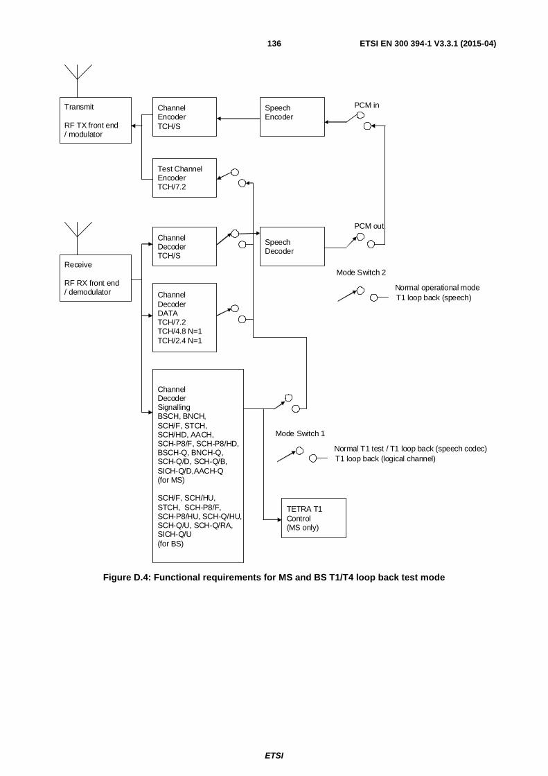
ETSI
ETSI EN 300 394-1 V3.3.1 (2015-04)136
Figure D.4: Functional requirements for MS and BS T1/T4 loop back test mode
ChannelEncoderTCH/S
PCM out
Mode Switch 2
Normal operational modeT1 loop back (speech)
SpeechDecoder
SpeechEncoder
ChannelDecoderTCH/S
PCM inTransmit
RF TX front end/ modulator
Test ChannelEncoderTCH/7.2
ChannelDecoderDATATCH/7.2TCH/4.8 N=1TCH/2.4 N=1
ChannelDecoderSignallingBSCH, BNCH,SCH/F, STCH,SCH/HD, AACH,SCH-P8/F, SCH-P8/HD,BSCH-Q, BNCH-Q,SCH-Q/D, SCH-Q/B,SICH-Q/D,AACH-Q(for MS)
SCH/F, SCH/HU,STCH, SCH-P8/F,SCH-P8/HU, SCH-Q/HU,SCH-Q/U, SCH-Q/RA,SICH-Q/U(for BS)
Receive
RF RX front end/ demodulator
Mode Switch 1
Normal T1 test / T1 loop back (speech codec)T1 loop back (logical channel)
TETRA T1Control(MS only)
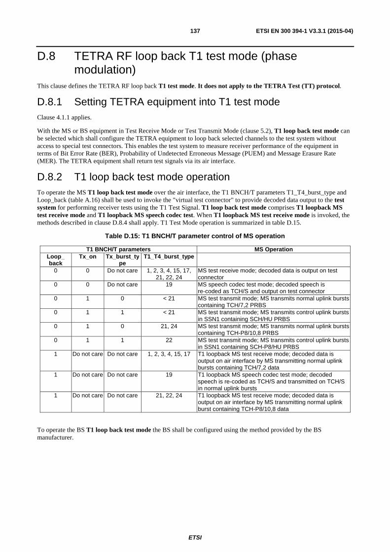
ETSI
ETSI EN 300 394-1 V3.3.1 (2015-04)137
D.8 TETRA RF loop back T1 test mode (phase modulation)
This clause defines the TETRA RF loop back T1 test mode. It does not apply to the TETRA Test (TT) protocol.
D.8.1 Setting TETRA equipment into T1 test mode Clause 4.1.1 applies.
With the MS or BS equipment in Test Receive Mode or Test Transmit Mode (clause 5.2), T1 loop back test mode can be selected which shall configure the TETRA equipment to loop back selected channels to the test system without access to special test connectors. This enables the test system to measure receiver performance of the equipment in terms of Bit Error Rate (BER), Probability of Undetected Erroneous Message (PUEM) and Message Erasure Rate (MER). The TETRA equipment shall return test signals via its air interface.
D.8.2 T1 loop back test mode operation To operate the MS T1 loop back test mode over the air interface, the T1 BNCH/T parameters T1_T4_burst_type and Loop_back (table A.16) shall be used to invoke the "virtual test connector" to provide decoded data output to the test system for performing receiver tests using the T1 Test Signal. T1 loop back test mode comprises T1 loopback MS test receive mode and T1 loopback MS speech codec test. When T1 loopback MS test receive mode is invoked, the methods described in clause D.8.4 shall apply. T1 Test Mode operation is summarized in table D.15.
Table D.15: T1 BNCH/T parameter control of MS operation
T1 BNCH/T parameters MS Operation Loop_ back
Tx_on Tx_burst_type
T1_T4_burst_type
0 0 Do not care 1, 2, 3, 4, 15, 17, 21, 22, 24
MS test receive mode; decoded data is output on test connector
0 0 Do not care 19 MS speech codec test mode; decoded speech is re-coded as TCH/S and output on test connector
0 1 0 < 21 MS test transmit mode; MS transmits normal uplink bursts containing TCH/7,2 PRBS
0 1 1 < 21 MS test transmit mode; MS transmits control uplink bursts in SSN1 containing SCH/HU PRBS
0 1 0 21, 24 MS test transmit mode; MS transmits normal uplink bursts containing TCH-P8/10,8 PRBS
0 1 1 22 MS test transmit mode; MS transmits control uplink bursts in SSN1 containing SCH-P8/HU PRBS
1 Do not care Do not care 1, 2, 3, 4, 15, 17 T1 loopback MS test receive mode; decoded data is output on air interface by MS transmitting normal uplink bursts containing TCH/7,2 data
1 Do not care Do not care 19 T1 loopback MS speech codec test mode; decoded speech is re-coded as TCH/S and transmitted on TCH/S in normal uplink bursts
1 Do not care Do not care 21, 22, 24 T1 loopback MS test receive mode; decoded data is output on air interface by MS transmitting normal uplink burst containing TCH-P8/10,8 data
To operate the BS T1 loop back test mode the BS shall be configured using the method provided by the BS manufacturer.
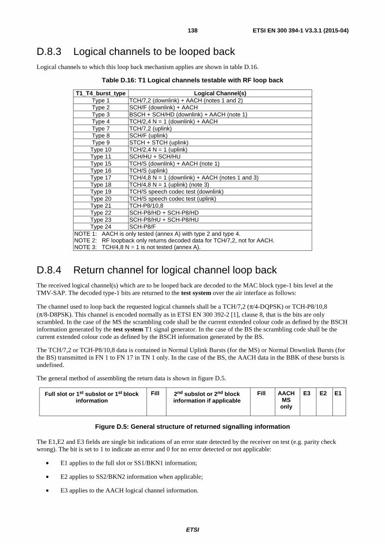
ETSI
ETSI EN 300 394-1 V3.3.1 (2015-04)138
D.8.3 Logical channels to be looped back Logical channels to which this loop back mechanism applies are shown in table D.16.
Table D.16: T1 Logical channels testable with RF loop back
T1_T4_burst_type Logical Channel(s) Type 1 TCH/7,2 (downlink) + AACH (notes 1 and 2) Type 2 SCH/F (downlink) + AACH Type 3 BSCH + SCH/HD (downlink) + AACH (note 1) Type 4 TCH/2,4 N = 1 (downlink) + AACH Type 7 TCH/7,2 (uplink) Type 8 SCH/F (uplink) Type 9 STCH + STCH (uplink)
Type 10 TCH/2,4 N = 1 (uplink) Type 11 SCH/HU + SCH/HU Type 15 TCH/S (downlink) + AACH (note 1) Type 16 TCH/S (uplink) Type 17 TCH/4,8 N = 1 (downlink) + AACH (notes 1 and 3) Type 18 TCH/4,8 N = 1 (uplink) (note 3) Type 19 TCH/S speech codec test (downlink) Type 20 TCH/S speech codec test (uplink) Type 21 TCH-P8/10,8 Type 22 SCH-P8/HD + SCH-P8/HD Type 23 SCH-P8/HU + SCH-P8/HU Type 24 SCH-P8/F
NOTE 1: AACH is only tested (annex A) with type 2 and type 4. NOTE 2: RF loopback only returns decoded data for TCH/7,2, not for AACH. NOTE 3: TCH/4,8 N = 1 is not tested (annex A).
D.8.4 Return channel for logical channel loop back The received logical channel(s) which are to be looped back are decoded to the MAC block type-1 bits level at the TMV-SAP. The decoded type-1 bits are returned to the test system over the air interface as follows:
The channel used to loop back the requested logical channels shall be a TCH/7,2 (π/4-DQPSK) or TCH-P8/10,8 (π/8-D8PSK). This channel is encoded normally as in ETSI EN 300 392-2 [1], clause 8, that is the bits are only scrambled. In the case of the MS the scrambling code shall be the current extended colour code as defined by the BSCH information generated by the test system T1 signal generator. In the case of the BS the scrambling code shall be the current extended colour code as defined by the BSCH information generated by the BS.
The TCH/7,2 or TCH-P8/10,8 data is contained in Normal Uplink Bursts (for the MS) or Normal Downlink Bursts (for the BS) transmitted in FN 1 to FN 17 in TN 1 only. In the case of the BS, the AACH data in the BBK of these bursts is undefined.
The general method of assembling the return data is shown in figure D.5.
Full slot or 1st subslot or 1st block information
Fill 2nd subslot or 2nd block information if applicable
Fill AACH MS
only
E3
E2
E1
Figure D.5: General structure of returned signalling information
The E1,E2 and E3 fields are single bit indications of an error state detected by the receiver on test (e.g. parity check wrong). The bit is set to 1 to indicate an error and 0 for no error detected or not applicable:
• E1 applies to the full slot or SS1/BKN1 information;
• E2 applies to SS2/BKN2 information when applicable;
• E3 applies to the AACH logical channel information.
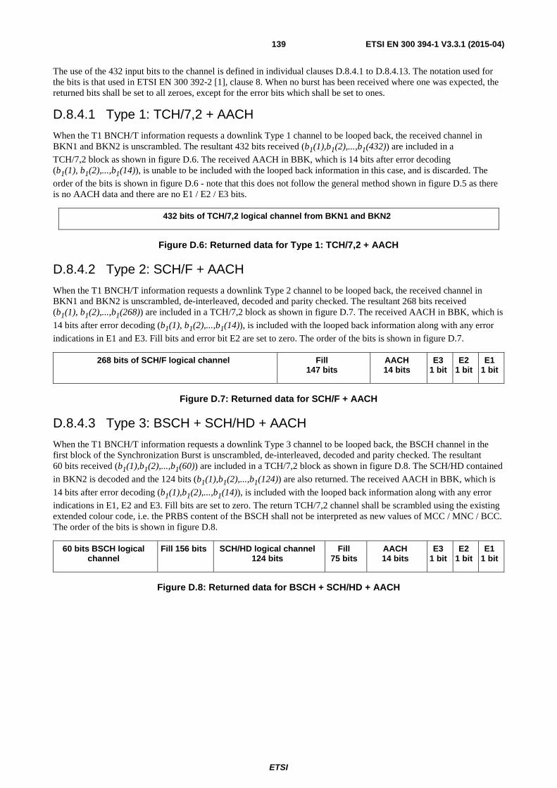
ETSI
ETSI EN 300 394-1 V3.3.1 (2015-04)139
The use of the 432 input bits to the channel is defined in individual clauses D.8.4.1 to D.8.4.13. The notation used for the bits is that used in ETSI EN 300 392-2 [1], clause 8. When no burst has been received where one was expected, the returned bits shall be set to all zeroes, except for the error bits which shall be set to ones.
D.8.4.1 Type 1: TCH/7,2 + AACH
When the T1 BNCH/T information requests a downlink Type 1 channel to be looped back, the received channel in BKN1 and BKN2 is unscrambled. The resultant 432 bits received (b1(1),b1(2),...,b1(432)) are included in a
TCH/7,2 block as shown in figure D.6. The received AACH in BBK, which is 14 bits after error decoding (b1(1), b1(2),...,b1(14)), is unable to be included with the looped back information in this case, and is discarded. The
order of the bits is shown in figure D.6 - note that this does not follow the general method shown in figure D.5 as there is no AACH data and there are no E1 / E2 / E3 bits.
432 bits of TCH/7,2 logical channel from BKN1 and BKN2
Figure D.6: Returned data for Type 1: TCH/7,2 + AACH
D.8.4.2 Type 2: SCH/F + AACH
When the T1 BNCH/T information requests a downlink Type 2 channel to be looped back, the received channel in BKN1 and BKN2 is unscrambled, de-interleaved, decoded and parity checked. The resultant 268 bits received (b1(1), b1(2),...,b1(268)) are included in a TCH/7,2 block as shown in figure D.7. The received AACH in BBK, which is
14 bits after error decoding (b1(1), b1(2),...,b1(14)), is included with the looped back information along with any error
indications in E1 and E3. Fill bits and error bit E2 are set to zero. The order of the bits is shown in figure D.7.
268 bits of SCH/F logical channel Fill 147 bits
AACH 14 bits
E3 1 bit
E2 1 bit
E1 1 bit
Figure D.7: Returned data for SCH/F + AACH
D.8.4.3 Type 3: BSCH + SCH/HD + AACH
When the T1 BNCH/T information requests a downlink Type 3 channel to be looped back, the BSCH channel in the first block of the Synchronization Burst is unscrambled, de-interleaved, decoded and parity checked. The resultant 60 bits received (b1(1),b1(2),...,b1(60)) are included in a TCH/7,2 block as shown in figure D.8. The SCH/HD contained
in BKN2 is decoded and the 124 bits (b1(1),b1(2),...,b1(124)) are also returned. The received AACH in BBK, which is
14 bits after error decoding (b1(1),b1(2),...,b1(14)), is included with the looped back information along with any error
indications in E1, E2 and E3. Fill bits are set to zero. The return TCH/7,2 channel shall be scrambled using the existing extended colour code, i.e. the PRBS content of the BSCH shall not be interpreted as new values of MCC / MNC / BCC. The order of the bits is shown in figure D.8.
60 bits BSCH logical channel
Fill 156 bits SCH/HD logical channel 124 bits
Fill 75 bits
AACH 14 bits
E3 1 bit
E2 1 bit
E1 1 bit
Figure D.8: Returned data for BSCH + SCH/HD + AACH
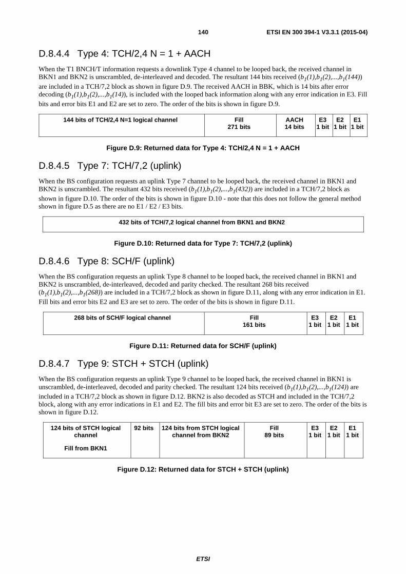
ETSI
ETSI EN 300 394-1 V3.3.1 (2015-04)140
D.8.4.4 Type 4: TCH/2,4 N = 1 + AACH
When the T1 BNCH/T information requests a downlink Type 4 channel to be looped back, the received channel in BKN1 and BKN2 is unscrambled, de-interleaved and decoded. The resultant 144 bits received (b1(1),b1(2),...,b1(144))
are included in a TCH/7,2 block as shown in figure D.9. The received AACH in BBK, which is 14 bits after error decoding (b1(1),b1(2),...,b1(14)), is included with the looped back information along with any error indication in E3. Fill
bits and error bits E1 and E2 are set to zero. The order of the bits is shown in figure D.9.
144 bits of TCH/2,4 N=1 logical channel Fill 271 bits
AACH 14 bits
E3 1 bit
E2 1 bit
E1 1 bit
Figure D.9: Returned data for Type 4: TCH/2,4 N = 1 + AACH
D.8.4.5 Type 7: TCH/7,2 (uplink)
When the BS configuration requests an uplink Type 7 channel to be looped back, the received channel in BKN1 and BKN2 is unscrambled. The resultant 432 bits received (b1(1),b1(2),...,b1(432)) are included in a TCH/7,2 block as
shown in figure D.10. The order of the bits is shown in figure D.10 - note that this does not follow the general method shown in figure D.5 as there are no E1 / E2 / E3 bits.
432 bits of TCH/7,2 logical channel from BKN1 and BKN2
Figure D.10: Returned data for Type 7: TCH/7,2 (uplink)
D.8.4.6 Type 8: SCH/F (uplink)
When the BS configuration requests an uplink Type 8 channel to be looped back, the received channel in BKN1 and BKN2 is unscrambled, de-interleaved, decoded and parity checked. The resultant 268 bits received (b1(1),b1(2),...,b1(268)) are included in a TCH/7,2 block as shown in figure D.11, along with any error indication in E1.
Fill bits and error bits E2 and E3 are set to zero. The order of the bits is shown in figure D.11.
268 bits of SCH/F logical channel Fill 161 bits
E3 1 bit
E2 1 bit
E1 1 bit
Figure D.11: Returned data for SCH/F (uplink)
D.8.4.7 Type 9: STCH + STCH (uplink)
When the BS configuration requests an uplink Type 9 channel to be looped back, the received channel in BKN1 is unscrambled, de-interleaved, decoded and parity checked. The resultant 124 bits received (b1(1),b1(2),...,b1(124)) are
included in a TCH/7,2 block as shown in figure D.12. BKN2 is also decoded as STCH and included in the TCH/7,2 block, along with any error indications in E1 and E2. The fill bits and error bit E3 are set to zero. The order of the bits is shown in figure D.12.
124 bits of STCH logical channel
Fill from BKN1
92 bits 124 bits from STCH logical channel from BKN2
Fill 89 bits
E3 1 bit
E2 1 bit
E1 1 bit
Figure D.12: Returned data for STCH + STCH (uplink)

ETSI
ETSI EN 300 394-1 V3.3.1 (2015-04)141
D.8.4.8 Type 10: TCH/2,4 N = 1 (uplink)
When the BS configuration requests an uplink Type 10 channel to be looped back, the received channel in BKN1 and BKN2 is unscrambled, de-interleaved and decoded. The resultant 144 bits received (b1(1),b1(2),...,b1(144)) are included
in a TCH/7,2 block as shown in figure D.13. Fill bits and error bits are set to zero. The order of the bits is shown in figure D.13.
144 bits of TCH/2.4 N=1 logical channel Fill 285 bits
E3 1 bit
E2 1 bit
E1 1 bit
Figure D.13: Returned data for Type 10: TCH/2,4 N = 1 + AACH
D.8.4.9 Type 11: SCH/HU + SCH/HU
When the BS configuration requests an uplink Type 11 channel to be looped back, then, if present, the received channel in SS1 is unscrambled, de-interleaved, decoded and parity checked. The resultant 92 bits received (b1(1),b1(2),...,b1(92)) are included in a TCH/7,2 block as shown in figure D.14, along with any error indication in E1.
If the second half of the received slot SS2 contains a SCH/HU the decoded 92 bits (b1(1),b1(2),...,b1(92))are returned,
along with any error indication in E2. Fill bits and error bit E3 are set to zero. The order of the bits is shown in figure D.14.
92 bits from SCH/HU logical channel in subslot 11
Fill 124 bits
92 bits from SCH/HU logical channel in
subslot 2
Fill 121 bits
E3 1 bit
E2 1 bit
E1 1 bit
Figure D.14: Returned data for SCH/HU + SCH/HU
D.8.4.10 Type 15: TCH/S + TCH/S + AACH
When the T1 BNCH/T information requests a downlink Type 15 channel to be looped back, the received channel in BKN1 and BKN2 is unscrambled, de-interleaved and decoded. The resultant 2 × 137 bits received (b1(1),b1(2),...,b1(137)) are included in a TCH/7,2 block as shown in figure D.15. The received AACH in BBK, which
is 14 bits after error decoding (b1(1),b1(2),...,b1(14)), is included with the looped back information along with any error
indications in E1 and E3. Fill bits and error bit E2 are set to zero. The order of the bits is shown in figure D.15.
TCH/S logical channel 137 bits Speech Sample A
Fill 79 bits
TCH/S logical channel 137 bits Speech Sample B
Fill 62 bits
AACH
14 bits
E3 1 bit
E2 1 bit
E1 1 bit
Figure D.15: Returned data for TCH/S + TCH/S + AACH
D.8.4.11 Type 16: TCH/S + TCH/S (uplink)
When the BS configuration requests an uplink Type 16 channel to be looped back, the received channel in BKN1 and BKN2 is unscrambled, de-interleaved and decoded. The resultant 2 × 137 bits received (b1(1),b1(2),...,b1(137)) are
included in a TCH/7,2 block as shown in figure D.16, along with any error indication in E1. Fill bits and error bits E2 and E3 are set to zero. The order of the bits is shown in figure D.16.
TCH/S logical channel 137 bits Speech Sample A
Fill 79 bits
TCH/S logical channel 137 bits Speech Sample B
Fill 76 bits
E3 1 bit
E2 1 bit
E1 1 bit
Figure D.16: Returned data for TCH/S + TCH/S (uplink)
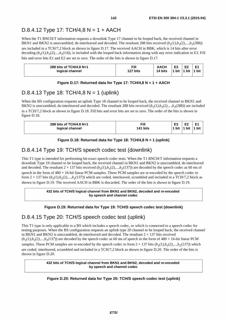
ETSI
ETSI EN 300 394-1 V3.3.1 (2015-04)142
D.8.4.12 Type 17: TCH/4,8 N = 1 + AACH
When the T1 BNCH/T information requests a downlink Type 17 channel to be looped back, the received channel in BKN1 and BKN2 is unscrambled, de-interleaved and decoded. The resultant 288 bits received (b1(1),b1(2),...,b1(288))
are included in a TCH/7,2 block as shown in figure D.17. The received AACH in BBK, which is 14 bits after error decoding (b1(1),b1(2),...,b1(14)), is included with the looped back information along with any error indication in E3. Fill
bits and error bits E1 and E2 are set to zero. The order of the bits is shown in figure D.17.
288 bits of TCH/4.8 N=1 logical channel
Fill 127 bits
AACH 14 bits
E3 1 bit
E2 1 bit
E1 1 bit
Figure D.17: Returned data for Type 17: TCH/4,8 N = 1 + AACH
D.8.4.13 Type 18: TCH/4,8 N = 1 (uplink)
When the BS configuration requests an uplink Type 18 channel to be looped back, the received channel in BKN1 and BKN2 is unscrambled, de-interleaved and decoded. The resultant 288 bits received (b1(1),b1(2),...,b1(288)) are included
in a TCH/7,2 block as shown in figure D.18. Fill bits and error bits are set to zero. The order of the bits is shown in figure D.18.
288 bits of TCH/4.8 N=1 logical channel
Fill 141 bits
E3 1 bit
E2 1 bit
E1 1 bit
Figure D.18: Returned data for Type 18: TCH/4,8 N = 1 (uplink)
D.8.4.14 Type 19: TCH/S speech codec test (downlink)
This T1 type is intended for performing bit-exact speech codec tests. When the T1 BNCH/T information requests a downlink Type 19 channel to be looped back, the received channel in BKN1 and BKN2 is unscrambled, de-interleaved and decoded. The resultant 2 × 137 bits received (b1(1),b1(2),...,b1(137)) are decoded by the speech codec as 60 ms of
speech in the form of 480 × 16-bit linear PCM samples. These PCM samples are re-encoded by the speech codec to form 2 × 137 bits (b1(1),b1(2),...,b1(137)) which are coded, interleaved, scrambled and included in a TCH/7,2 block as
shown in figure D.19. The received AACH in BBK is discarded. The order of the bits is shown in figure D.19.
432 bits of TCH/S logical channel from BKN1 and BKN2, decoded and re-encoded by speech and channel codec
Figure D.19: Returned data for Type 19: TCH/S speech codec test (downlink)
D.8.4.15 Type 20: TCH/S speech codec test (uplink)
This T1 type is only applicable to a BS which includes a speech codec, or which is connected to a speech codec for testing purposes. When the BS configuration requests an uplink type 20 channel to be looped back, the received channel in BKN1 and BKN2 is unscrambled, de-interleaved and decoded. The resultant 2 × 137 bits received (b1(1),b1(2),...,b1(137)) are decoded by the speech codec as 60 ms of speech in the form of 480 × 16-bit linear PCM
samples. These PCM samples are re-encoded by the speech codec to form 2 × 137 bits (b1(1),b1(2),...,b1(137)) which
are coded, interleaved, scrambled and included in a TCH/7,2 block as shown in figure D.20. The order of the bits is shown in figure D.20.
432 bits of TCH/S logical channel from BKN1 and BKN2, decoded and re-encoded by speech and channel codec
Figure D.20: Returned data for Type 20: TCH/S speech codec test (uplink)
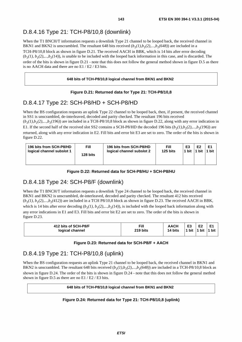
ETSI
ETSI EN 300 394-1 V3.3.1 (2015-04)143
D.8.4.16 Type 21: TCH-P8/10,8 (downlink)
When the T1 BNCH/T information requests a downlink Type 21 channel to be looped back, the received channel in BKN1 and BKN2 is unscrambled. The resultant 648 bits received (b1(1),b1(2),...,b1(648)) are included in a
TCH-P8/10,8 block as shown in figure D.21. The received AACH in BBK, which is 14 bits after error decoding (b1(1), b1(2),...,b1(14)), is unable to be included with the looped back information in this case, and is discarded. The
order of the bits is shown in figure D.21 - note that this does not follow the general method shown in figure D.5 as there is no AACH data and there are no E1 / E2 / E3 bits.
648 bits of TCH-P8/10,8 logical channel from BKN1 and BKN2
Figure D.21: Returned data for Type 21: TCH-P8/10,8
D.8.4.17 Type 22: SCH-P8/HD + SCH-P8/HD
When the BS configuration requests an uplink Type 22 channel to be looped back, then, if present, the received channel in SS1 is unscrambled, de-interleaved, decoded and parity checked. The resultant 196 bits received (b1(1),b1(2),...,b1(196)) are included in a TCH-P8/10,8 block as shown in figure D.22, along with any error indication in
E1. If the second half of the received slot SS2 contains a SCH-P8/HD the decoded 196 bits (b1(1),b1(2),...,b1(196)) are
returned, along with any error indication in E2. Fill bits and error bit E3 are set to zero. The order of the bits is shown in figure D.22.
196 bits from SCH-P8/HD logical channel subslot 1
Fill
128 bits
196 bits from SCH-P8/HD logical channel subslot 2
Fill 125 bits
E3 1 bit
E2 1 bit
E1 1 bit
Figure D.22: Returned data for SCH-P8/HU + SCH-P8/HU
D.8.4.18 Type 24: SCH-P8/F (downlink)
When the T1 BNCH/T information requests a downlink Type 24 channel to be looped back, the received channel in BKN1 and BKN2 is unscrambled, de-interleaved, decoded and parity checked. The resultant 412 bits received (b1(1), b1(2),...,b1(412)) are included in a TCH P8/10,8 block as shown in figure D.23. The received AACH in BBK,
which is 14 bits after error decoding (b1(1), b1(2),...,b1(14)), is included with the looped back information along with
any error indications in E1 and E3. Fill bits and error bit E2 are set to zero. The order of the bits is shown in figure D.23.
412 bits of SCH-P8/F logical channel
Fill 219 bits
AACH 14 bits
E3 1 bit
E2 1 bit
E1 1 bit
Figure D.23: Returned data for SCH-P8/F + AACH
D.8.4.19 Type 21: TCH-P8/10,8 (uplink)
When the BS configuration requests an uplink Type 21 channel to be looped back, the received channel in BKN1 and BKN2 is unscrambled. The resultant 648 bits received (b1(1),b1(2),...,b1(648)) are included in a TCH-P8/10,8 block as
shown in figure D.24. The order of the bits is shown in figure D.24 - note that this does not follow the general method shown in figure D.5 as there are no E1 / E2 / E3 bits.
648 bits of TCH-P8/10,8 logical channel from BKN1 and BKN2
Figure D.24: Returned data for Type 21: TCH-P8/10,8 (uplink)
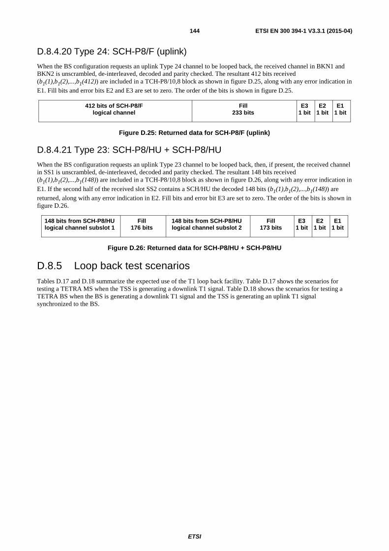
ETSI
ETSI EN 300 394-1 V3.3.1 (2015-04)144
D.8.4.20 Type 24: SCH-P8/F (uplink)
When the BS configuration requests an uplink Type 24 channel to be looped back, the received channel in BKN1 and BKN2 is unscrambled, de-interleaved, decoded and parity checked. The resultant 412 bits received (b1(1),b1(2),...,b1(412)) are included in a TCH-P8/10,8 block as shown in figure D.25, along with any error indication in
E1. Fill bits and error bits E2 and E3 are set to zero. The order of the bits is shown in figure D.25.
412 bits of SCH-P8/F logical channel
Fill 233 bits
E3 1 bit
E2 1 bit
E1 1 bit
Figure D.25: Returned data for SCH-P8/F (uplink)
D.8.4.21 Type 23: SCH-P8/HU + SCH-P8/HU
When the BS configuration requests an uplink Type 23 channel to be looped back, then, if present, the received channel in SS1 is unscrambled, de-interleaved, decoded and parity checked. The resultant 148 bits received (b1(1),b1(2),...,b1(148)) are included in a TCH-P8/10,8 block as shown in figure D.26, along with any error indication in
E1. If the second half of the received slot SS2 contains a SCH/HU the decoded 148 bits (b1(1),b1(2),...,b1(148)) are
returned, along with any error indication in E2. Fill bits and error bit E3 are set to zero. The order of the bits is shown in figure D.26.
148 bits from SCH-P8/HU logical channel subslot 1
Fill 176 bits
148 bits from SCH-P8/HU logical channel subslot 2
Fill 173 bits
E3 1 bit
E2 1 bit
E1 1 bit
Figure D.26: Returned data for SCH-P8/HU + SCH-P8/HU
D.8.5 Loop back test scenarios Tables D.17 and D.18 summarize the expected use of the T1 loop back facility. Table D.17 shows the scenarios for testing a TETRA MS when the TSS is generating a downlink T1 signal. Table D.18 shows the scenarios for testing a TETRA BS when the BS is generating a downlink T1 signal and the TSS is generating an uplink T1 signal synchronized to the BS.
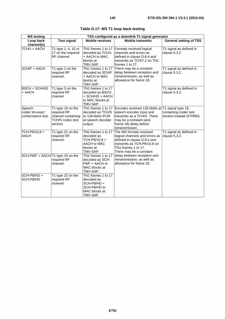
ETSI
ETSI EN 300 394-1 V3.3.1 (2015-04)145
Table D.17: MS T1 loop back testing
MS testing TSS configured as a downlink T1 signal generator Loop back channel(s)
Test signal Mobile receives Mobile transmits General setting of TSS
TCH/x + AACH T1 type 1, 4, 15 or 17 on the required RF channel.
TN1 frames 1 to 17 decoded as TCH/x + AACH to MAC blocks at TMV-SAP.
Formats received logical channels and errors as defined in clause D.8.4 and transmits as TCH/7,2 on TN1 frames 1 to 17. There may be a constant delay between reception and retransmission, as well as allowance for frame 18.
T1 signal as defined in clause 5.3.2.
SCH/F + AACH T1 type 2 on the required RF channel.
TN1 frames 1 to 17 decoded as SCH/F + AACH to MAC blocks at TMV-SAP.
T1 signal as defined in clause 5.3.2.
BSCH + SCH/HD + AACH
T1 type 3 on the required RF channel.
TN1 frames 1 to 17 decoded as BSCH + SCH/HD + AACH to MAC blocks at TMV-SAP.
T1 signal as defined in clause 5.3.2.
Speech codec bit-exact conformance test.
T1 type 19 on the required RF channel containing TCH/S codec test vectors.
TN1 frames 1 to 17 decoded as TCH/S to 128 kbit/s PCM at speech decoder output.
Encodes received 128 kbit/s at speech encoder input and transmits as a TCH/S. There may be a constant (and frame 18) delay before retransmission.
T1 signal type 19, containing codec test vectors instead of PRBS.
TCH-P8/10,8 + AACH
T1 type 21 on the required RF channel.
TN1 frames 1 to 17 decoded as TCH-P8/10,8 + AACH to MAC blocks at TMV-SAP.
The MS formats received logical channels and errors as defined in clause D.8.4 and transmits as TCH-P8/10,8 on TN1 frames 1 to 17. There may be a constant delay between reception and retransmission, as well as allowance for frame 18.
T1 signal as defined in clause 5.3.2.
SCH-P8/F + AACH T1 type 24 on the required RF channel.
TN1 frames 1 to 17 decoded as SCH-P8/F + AACH to MAC blocks at TMV-SAP.
SCH-P8/HD + SCH-P8/HD
T1 type 22 on the required RF channel.
TN1 frames 1 to 17 decoded as SCH-P8/HD + SCH-P8/HD to MAC blocks at TMV-SAP.
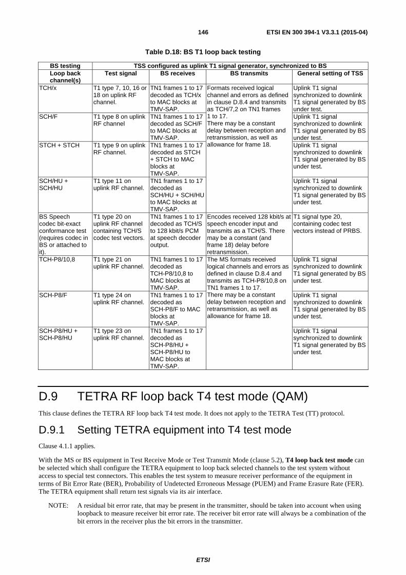
ETSI
ETSI EN 300 394-1 V3.3.1 (2015-04)146
Table D.18: BS T1 loop back testing
BS testing TSS configured as uplink T1 signal generator, synchronized to BS Loop back channel(s)
Test signal BS receives BS transmits General setting of TSS
TCH/x T1 type 7, 10, 16 or 18 on uplink RF channel.
TN1 frames 1 to 17 decoded as TCH/x to MAC blocks at TMV-SAP.
Formats received logical channel and errors as defined in clause D.8.4 and transmits as TCH/7,2 on TN1 frames 1 to 17. There may be a constant delay between reception and retransmission, as well as allowance for frame 18.
Uplink T1 signal synchronized to downlink T1 signal generated by BS under test.
SCH/F T1 type 8 on uplink RF channel
TN1 frames 1 to 17 decoded as SCH/F to MAC blocks at TMV-SAP.
Uplink T1 signal synchronized to downlink T1 signal generated by BS under test.
STCH + STCH T1 type 9 on uplink RF channel.
TN1 frames 1 to 17 decoded as STCH + STCH to MAC blocks at TMV-SAP.
Uplink T1 signal synchronized to downlink T1 signal generated by BS under test.
SCH/HU + SCH/HU
T1 type 11 on uplink RF channel.
TN1 frames 1 to 17 decoded as SCH/HU + SCH/HU to MAC blocks at TMV-SAP.
Uplink T1 signal synchronized to downlink T1 signal generated by BS under test.
BS Speech codec bit-exact conformance test (requires codec in BS or attached to it).
T1 type 20 on uplink RF channel containing TCH/S codec test vectors.
TN1 frames 1 to 17 decoded as TCH/S to 128 kbit/s PCM at speech decoder output.
Encodes received 128 kbit/s at speech encoder input and transmits as a TCH/S. There may be a constant (and frame 18) delay before retransmission.
T1 signal type 20, containing codec test vectors instead of PRBS.
TCH-P8/10,8 T1 type 21 on uplink RF channel.
TN1 frames 1 to 17 decoded as TCH-P8/10,8 to MAC blocks at TMV-SAP.
The MS formats received logical channels and errors as defined in clause D.8.4 and transmits as TCH-P8/10,8 on TN1 frames 1 to 17. There may be a constant delay between reception and retransmission, as well as allowance for frame 18.
Uplink T1 signal synchronized to downlink T1 signal generated by BS under test.
SCH-P8/F T1 type 24 on uplink RF channel.
TN1 frames 1 to 17 decoded as SCH-P8/F to MAC blocks at TMV-SAP.
Uplink T1 signal synchronized to downlink T1 signal generated by BS under test.
SCH-P8/HU + SCH-P8/HU
T1 type 23 on uplink RF channel.
TN1 frames 1 to 17 decoded as SCH-P8/HU + SCH-P8/HU to MAC blocks at TMV-SAP.
Uplink T1 signal synchronized to downlink T1 signal generated by BS under test.
D.9 TETRA RF loop back T4 test mode (QAM) This clause defines the TETRA RF loop back T4 test mode. It does not apply to the TETRA Test (TT) protocol.
D.9.1 Setting TETRA equipment into T4 test mode Clause 4.1.1 applies.
With the MS or BS equipment in Test Receive Mode or Test Transmit Mode (clause 5.2), T4 loop back test mode can be selected which shall configure the TETRA equipment to loop back selected channels to the test system without access to special test connectors. This enables the test system to measure receiver performance of the equipment in terms of Bit Error Rate (BER), Probability of Undetected Erroneous Message (PUEM) and Frame Erasure Rate (FER). The TETRA equipment shall return test signals via its air interface.
NOTE: A residual bit error rate, that may be present in the transmitter, should be taken into account when using loopback to measure receiver bit error rate. The receiver bit error rate will always be a combination of the bit errors in the receiver plus the bit errors in the transmitter.
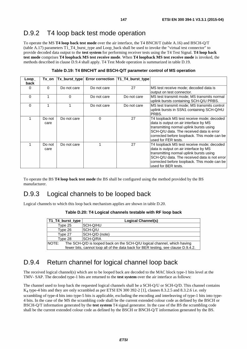
ETSI
ETSI EN 300 394-1 V3.3.1 (2015-04)147
D.9.2 T4 loop back test mode operation To operate the MS T4 loop back test mode over the air interface, the T4 BNCH/T (table A.16) and BSCH-Q/T (table A.17) parameters T1_T4_burst_type and Loop_back shall be used to invoke the "virtual test connector" to provide decoded data output to the test system for performing receiver tests using the T4 Test Signal. T4 loop back test mode comprises T4 loopback MS test receive mode. When T4 loopback MS test receive mode is invoked, the methods described in clause D.9.4 shall apply. T4 Test Mode operation is summarized in table D.19.
Table D.19: T4 BNCH/T and BSCH-Q/T parameter control of MS operation
Loop_ back
Tx_on Tx_burst_type Error correction T1_T4_burst_type
0 0 Do not care Do not care 27 MS test receive mode; decoded data is output on test connector.
0 1 0 Do not care Do not care MS test transmit mode; MS transmits normal uplink bursts containing SCH-Q/U PRBS.
0 1 1 Do not care Do not care MS test transmit mode; MS transmits control uplink bursts in SSN1 containing SCH-Q/HU PRBS.
1 Do not care
Do not care 0 27 T4 loopback MS test receive mode; decoded data is output on air interface by MS transmitting normal uplink bursts using SCH-Q/U data. The received data is error corrected before loopback. This mode can be used for FER tests.
1 Do not care
Do not care 1 27 T4 loopback MS test receive mode; decoded data is output on air interface by MS transmitting normal uplink bursts using SCH-Q/U data. The received data is not error corrected before loopback. This mode can be used for BER tests.
To operate the BS T4 loop back test mode the BS shall be configured using the method provided by the BS manufacturer.
D.9.3 Logical channels to be looped back Logical channels to which this loop back mechanism applies are shown in table D.20.
Table D.20: T4 Logical channels testable with RF loop back
T1_T4_burst_type Logical Channel(s) Type 25 SCH-Q/HU Type 26 SCH-Q/U Type 27 SCH-Q/D (note) Type 28 SCH-Q/RA
NOTE: The SCH-Q/D is looped back on the SCH-Q/U logical channel, which having fewer bits, cannot loop all of the data back for BER testing, see clause D.9.4.2.
D.9.4 Return channel for logical channel loop back The received logical channel(s) which are to be looped back are decoded to the MAC block type-1 bits level at the TMV- SAP. The decoded type-1 bits are returned to the test system over the air interface as follows:
The channel used to loop back the requested logical channels shall be a SCH-Q/U or SCH-Q/D. This channel contains K4 type-4 bits and they are only scrambled as per ETSI EN 300 392-2 [1], clauses 8.3.2.5 and 8.3.2.6 i.e. only scrambling of type-4 bits into type-5 bits is applicable, excluding the encoding and interleaving of type-1 bits into type-4 bits. In the case of the MS the scrambling code shall be the current extended colour code as defined by the BSCH or BSCH-Q/T information generated by the test system T4 signal generator. In the case of the BS the scrambling code shall be the current extended colour code as defined by the BSCH or BNCH-Q/T information generated by the BS.
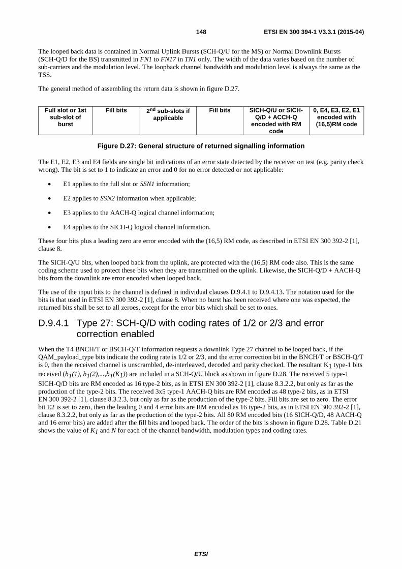
ETSI
ETSI EN 300 394-1 V3.3.1 (2015-04)148
The looped back data is contained in Normal Uplink Bursts (SCH-Q/U for the MS) or Normal Downlink Bursts (SCH-Q/D for the BS) transmitted in FN1 to FN17 in TN1 only. The width of the data varies based on the number of sub-carriers and the modulation level. The loopback channel bandwidth and modulation level is always the same as the TSS.
The general method of assembling the return data is shown in figure D.27.
Full slot or 1st
sub-slot of burst
Fill bits 2nd sub-slots if applicable
Fill bits SICH-Q/U or SICH-Q/D + ACCH-Q
encoded with RM code
0, E4, E3, E2, E1 encoded with (16,5)RM code
Figure D.27: General structure of returned signalling information
The E1, E2, E3 and E4 fields are single bit indications of an error state detected by the receiver on test (e.g. parity check wrong). The bit is set to 1 to indicate an error and 0 for no error detected or not applicable:
• E1 applies to the full slot or SSN1 information;
• E2 applies to SSN2 information when applicable;
• E3 applies to the AACH-Q logical channel information;
• E4 applies to the SICH-Q logical channel information.
These four bits plus a leading zero are error encoded with the (16,5) RM code, as described in ETSI EN 300 392-2 [1], clause 8.
The SICH-Q/U bits, when looped back from the uplink, are protected with the (16,5) RM code also. This is the same coding scheme used to protect these bits when they are transmitted on the uplink. Likewise, the SICH-Q/D + AACH-Q bits from the downlink are error encoded when looped back.
The use of the input bits to the channel is defined in individual clauses D.9.4.1 to D.9.4.13. The notation used for the bits is that used in ETSI EN 300 392-2 [1], clause 8. When no burst has been received where one was expected, the returned bits shall be set to all zeroes, except for the error bits which shall be set to ones.
D.9.4.1 Type 27: SCH-Q/D with coding rates of 1/2 or 2/3 and error correction enabled
When the T4 BNCH/T or BSCH-Q/T information requests a downlink Type 27 channel to be looped back, if the QAM_payload_type bits indicate the coding rate is 1/2 or 2/3, and the error correction bit in the BNCH/T or BSCH-Q/T is 0, then the received channel is unscrambled, de-interleaved, decoded and parity checked. The resultant K1 type-1 bits received (b1(1), b1(2),...,b1(K1)) are included in a SCH-Q/U block as shown in figure D.28. The received 5 type-1
SICH-Q/D bits are RM encoded as 16 type-2 bits, as in ETSI EN 300 392-2 [1], clause 8.3.2.2, but only as far as the production of the type-2 bits. The received 3x5 type-1 AACH-Q bits are RM encoded as 48 type-2 bits, as in ETSI EN 300 392-2 [1], clause 8.3.2.3, but only as far as the production of the type-2 bits. Fill bits are set to zero. The error bit E2 is set to zero, then the leading 0 and 4 error bits are RM encoded as 16 type-2 bits, as in ETSI EN 300 392-2 [1], clause 8.3.2.2, but only as far as the production of the type-2 bits. All 80 RM encoded bits (16 SICH-Q/D, 48 AACH-Q and 16 error bits) are added after the fill bits and looped back. The order of the bits is shown in figure D.28. Table D.21 shows the value of K1 and N for each of the channel bandwidth, modulation types and coding rates.
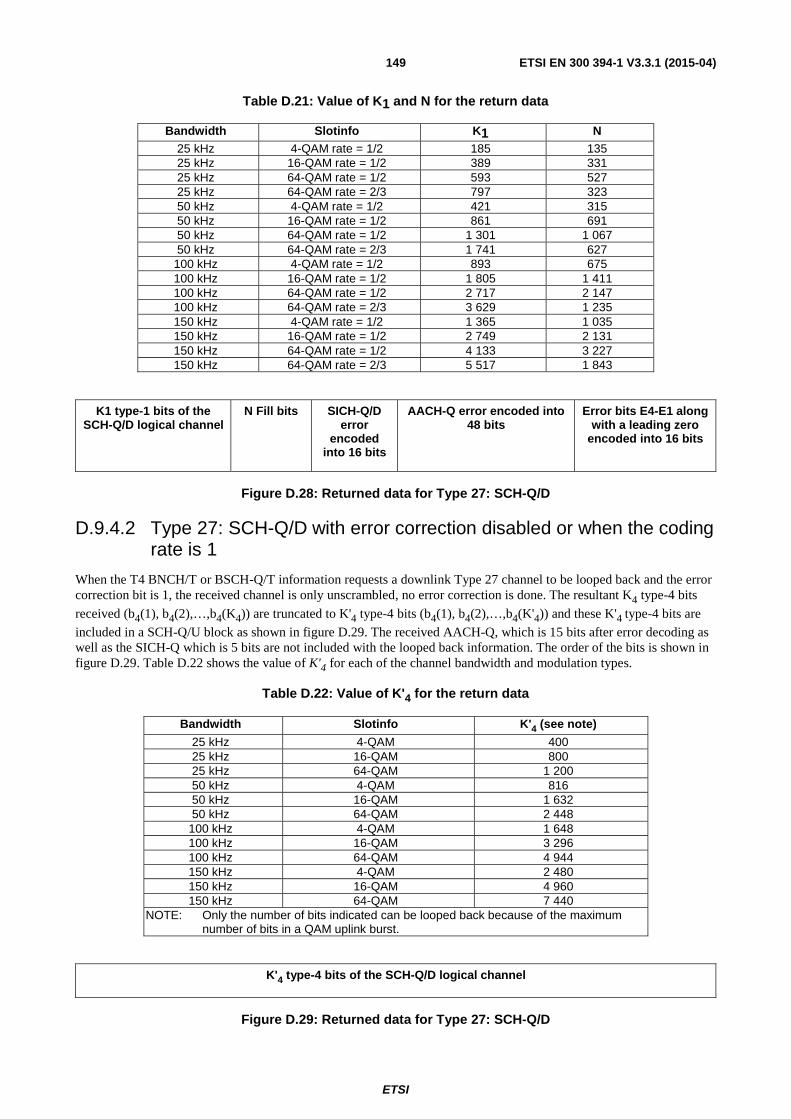
ETSI
ETSI EN 300 394-1 V3.3.1 (2015-04)149
Table D.21: Value of K1 and N for the return data
Bandwidth Slotinfo K1 N 25 kHz 4-QAM rate = 1/2 185 135 25 kHz 16-QAM rate = 1/2 389 331 25 kHz 64-QAM rate = 1/2 593 527 25 kHz 64-QAM rate = 2/3 797 323 50 kHz 4-QAM rate = 1/2 421 315 50 kHz 16-QAM rate = 1/2 861 691 50 kHz 64-QAM rate = 1/2 1 301 1 067 50 kHz 64-QAM rate = 2/3 1 741 627
100 kHz 4-QAM rate = 1/2 893 675 100 kHz 16-QAM rate = 1/2 1 805 1 411 100 kHz 64-QAM rate = 1/2 2 717 2 147 100 kHz 64-QAM rate = 2/3 3 629 1 235 150 kHz 4-QAM rate = 1/2 1 365 1 035 150 kHz 16-QAM rate = 1/2 2 749 2 131 150 kHz 64-QAM rate = 1/2 4 133 3 227 150 kHz 64-QAM rate = 2/3 5 517 1 843
K1 type-1 bits of the SCH-Q/D logical channel
N Fill bits SICH-Q/D error
encoded into 16 bits
AACH-Q error encoded into 48 bits
Error bits E4-E1 along with a leading zero
encoded into 16 bits
Figure D.28: Returned data for Type 27: SCH-Q/D
D.9.4.2 Type 27: SCH-Q/D with error correction disabled or when the coding rate is 1
When the T4 BNCH/T or BSCH-Q/T information requests a downlink Type 27 channel to be looped back and the error correction bit is 1, the received channel is only unscrambled, no error correction is done. The resultant K4 type-4 bits
received (b4(1), b4(2),…,b4(K4)) are truncated to K'4 type-4 bits (b4(1), b4(2),…,b4(K'4)) and these K'4 type-4 bits are
included in a SCH-Q/U block as shown in figure D.29. The received AACH-Q, which is 15 bits after error decoding as well as the SICH-Q which is 5 bits are not included with the looped back information. The order of the bits is shown in figure D.29. Table D.22 shows the value of K'4 for each of the channel bandwidth and modulation types.
Table D.22: Value of K'4 for the return data
Bandwidth Slotinfo K'4 (see note)
25 kHz 4-QAM 400 25 kHz 16-QAM 800 25 kHz 64-QAM 1 200 50 kHz 4-QAM 816 50 kHz 16-QAM 1 632 50 kHz 64-QAM 2 448
100 kHz 4-QAM 1 648 100 kHz 16-QAM 3 296 100 kHz 64-QAM 4 944 150 kHz 4-QAM 2 480 150 kHz 16-QAM 4 960 150 kHz 64-QAM 7 440
NOTE: Only the number of bits indicated can be looped back because of the maximum number of bits in a QAM uplink burst.
K'4 type-4 bits of the SCH-Q/D logical channel
Figure D.29: Returned data for Type 27: SCH-Q/D
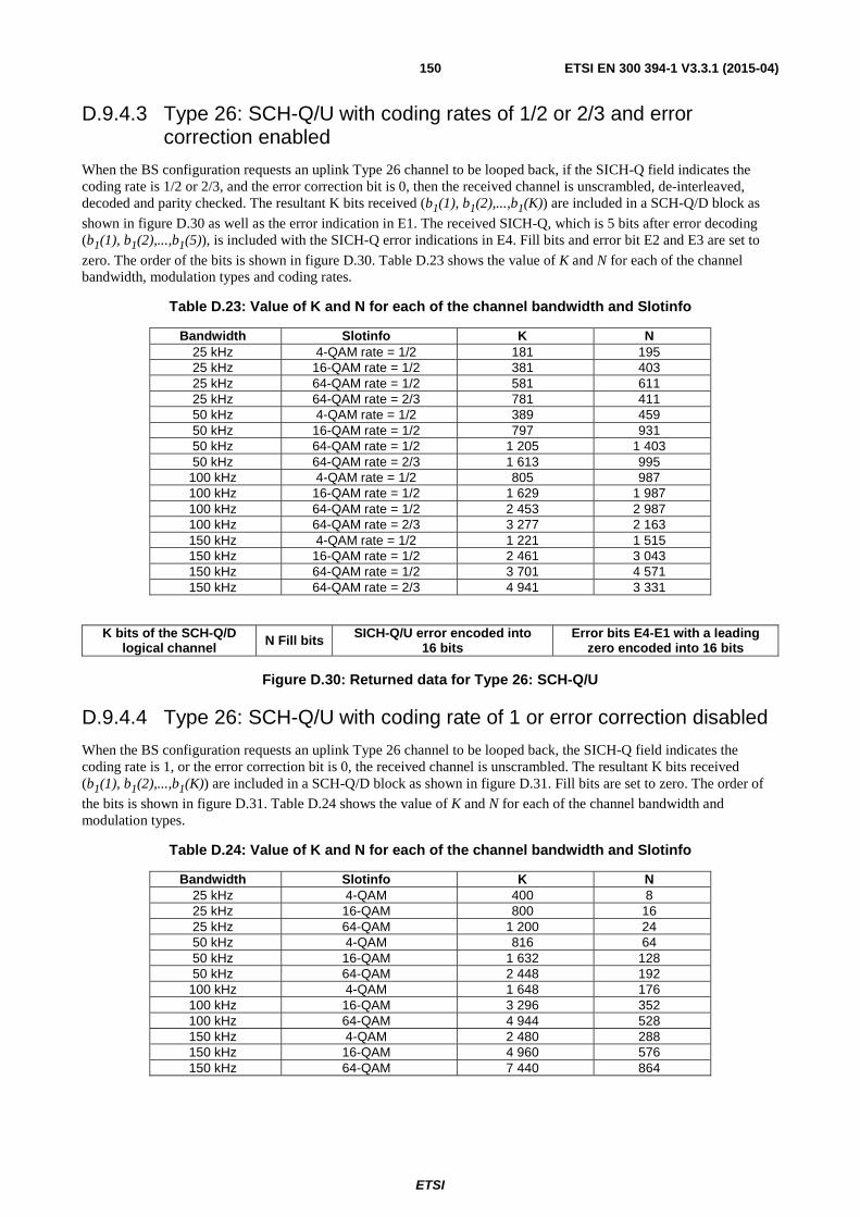
ETSI
ETSI EN 300 394-1 V3.3.1 (2015-04)150
D.9.4.3 Type 26: SCH-Q/U with coding rates of 1/2 or 2/3 and error correction enabled
When the BS configuration requests an uplink Type 26 channel to be looped back, if the SICH-Q field indicates the coding rate is 1/2 or 2/3, and the error correction bit is 0, then the received channel is unscrambled, de-interleaved, decoded and parity checked. The resultant K bits received (b1(1), b1(2),...,b1(K)) are included in a SCH-Q/D block as
shown in figure D.30 as well as the error indication in E1. The received SICH-Q, which is 5 bits after error decoding (b1(1), b1(2),...,b1(5)), is included with the SICH-Q error indications in E4. Fill bits and error bit E2 and E3 are set to
zero. The order of the bits is shown in figure D.30. Table D.23 shows the value of K and N for each of the channel bandwidth, modulation types and coding rates.
Table D.23: Value of K and N for each of the channel bandwidth and Slotinfo
Bandwidth Slotinfo K N 25 kHz 4-QAM rate = 1/2 181 195 25 kHz 16-QAM rate = 1/2 381 403 25 kHz 64-QAM rate = 1/2 581 611 25 kHz 64-QAM rate = 2/3 781 411 50 kHz 4-QAM rate = 1/2 389 459 50 kHz 16-QAM rate = 1/2 797 931 50 kHz 64-QAM rate = 1/2 1 205 1 403 50 kHz 64-QAM rate = 2/3 1 613 995
100 kHz 4-QAM rate = 1/2 805 987 100 kHz 16-QAM rate = 1/2 1 629 1 987 100 kHz 64-QAM rate = 1/2 2 453 2 987 100 kHz 64-QAM rate = 2/3 3 277 2 163 150 kHz 4-QAM rate = 1/2 1 221 1 515 150 kHz 16-QAM rate = 1/2 2 461 3 043 150 kHz 64-QAM rate = 1/2 3 701 4 571 150 kHz 64-QAM rate = 2/3 4 941 3 331
K bits of the SCH-Q/D logical channel N Fill bits SICH-Q/U error encoded into
16 bits Error bits E4-E1 with a leading
zero encoded into 16 bits
Figure D.30: Returned data for Type 26: SCH-Q/U
D.9.4.4 Type 26: SCH-Q/U with coding rate of 1 or error correction disabled
When the BS configuration requests an uplink Type 26 channel to be looped back, the SICH-Q field indicates the coding rate is 1, or the error correction bit is 0, the received channel is unscrambled. The resultant K bits received (b1(1), b1(2),...,b1(K)) are included in a SCH-Q/D block as shown in figure D.31. Fill bits are set to zero. The order of
the bits is shown in figure D.31. Table D.24 shows the value of K and N for each of the channel bandwidth and modulation types.
Table D.24: Value of K and N for each of the channel bandwidth and Slotinfo
Bandwidth Slotinfo K N 25 kHz 4-QAM 400 8 25 kHz 16-QAM 800 16 25 kHz 64-QAM 1 200 24 50 kHz 4-QAM 816 64 50 kHz 16-QAM 1 632 128 50 kHz 64-QAM 2 448 192
100 kHz 4-QAM 1 648 176 100 kHz 16-QAM 3 296 352 100 kHz 64-QAM 4 944 528 150 kHz 4-QAM 2 480 288 150 kHz 16-QAM 4 960 576 150 kHz 64-QAM 7 440 864
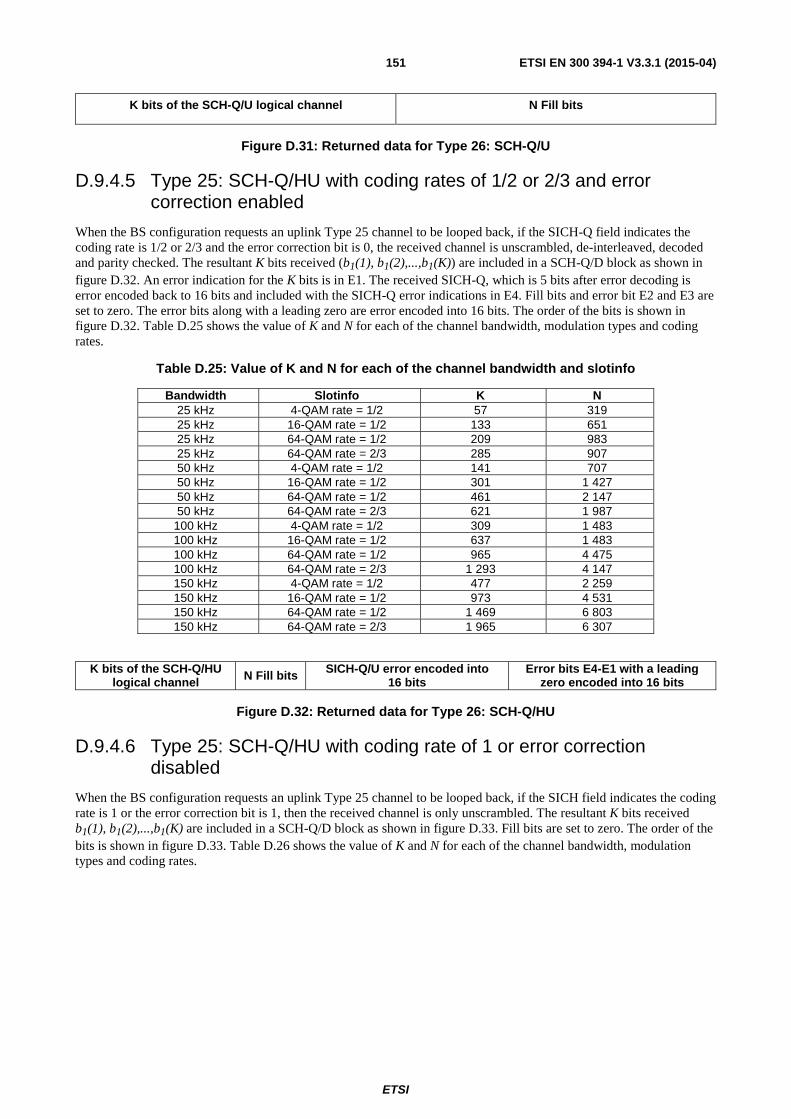
ETSI
ETSI EN 300 394-1 V3.3.1 (2015-04)151
K bits of the SCH-Q/U logical channel N Fill bits
Figure D.31: Returned data for Type 26: SCH-Q/U
D.9.4.5 Type 25: SCH-Q/HU with coding rates of 1/2 or 2/3 and error correction enabled
When the BS configuration requests an uplink Type 25 channel to be looped back, if the SICH-Q field indicates the coding rate is 1/2 or 2/3 and the error correction bit is 0, the received channel is unscrambled, de-interleaved, decoded and parity checked. The resultant K bits received (b1(1), b1(2),...,b1(K)) are included in a SCH-Q/D block as shown in figure D.32. An error indication for the K bits is in E1. The received SICH-Q, which is 5 bits after error decoding is error encoded back to 16 bits and included with the SICH-Q error indications in E4. Fill bits and error bit E2 and E3 are set to zero. The error bits along with a leading zero are error encoded into 16 bits. The order of the bits is shown in figure D.32. Table D.25 shows the value of K and N for each of the channel bandwidth, modulation types and coding rates.
Table D.25: Value of K and N for each of the channel bandwidth and slotinfo
Bandwidth Slotinfo K N 25 kHz 4-QAM rate = 1/2 57 319 25 kHz 16-QAM rate = 1/2 133 651 25 kHz 64-QAM rate = 1/2 209 983 25 kHz 64-QAM rate = 2/3 285 907 50 kHz 4-QAM rate = 1/2 141 707 50 kHz 16-QAM rate = 1/2 301 1 427 50 kHz 64-QAM rate = 1/2 461 2 147 50 kHz 64-QAM rate = 2/3 621 1 987
100 kHz 4-QAM rate = 1/2 309 1 483 100 kHz 16-QAM rate = 1/2 637 1 483 100 kHz 64-QAM rate = 1/2 965 4 475 100 kHz 64-QAM rate = 2/3 1 293 4 147 150 kHz 4-QAM rate = 1/2 477 2 259 150 kHz 16-QAM rate = 1/2 973 4 531 150 kHz 64-QAM rate = 1/2 1 469 6 803 150 kHz 64-QAM rate = 2/3 1 965 6 307
K bits of the SCH-Q/HU logical channel N Fill bits SICH-Q/U error encoded into
16 bits Error bits E4-E1 with a leading
zero encoded into 16 bits
Figure D.32: Returned data for Type 26: SCH-Q/HU
D.9.4.6 Type 25: SCH-Q/HU with coding rate of 1 or error correction disabled
When the BS configuration requests an uplink Type 25 channel to be looped back, if the SICH field indicates the coding rate is 1 or the error correction bit is 1, then the received channel is only unscrambled. The resultant K bits received b1(1), b1(2),...,b1(K) are included in a SCH-Q/D block as shown in figure D.33. Fill bits are set to zero. The order of the bits is shown in figure D.33. Table D.26 shows the value of K and N for each of the channel bandwidth, modulation types and coding rates.
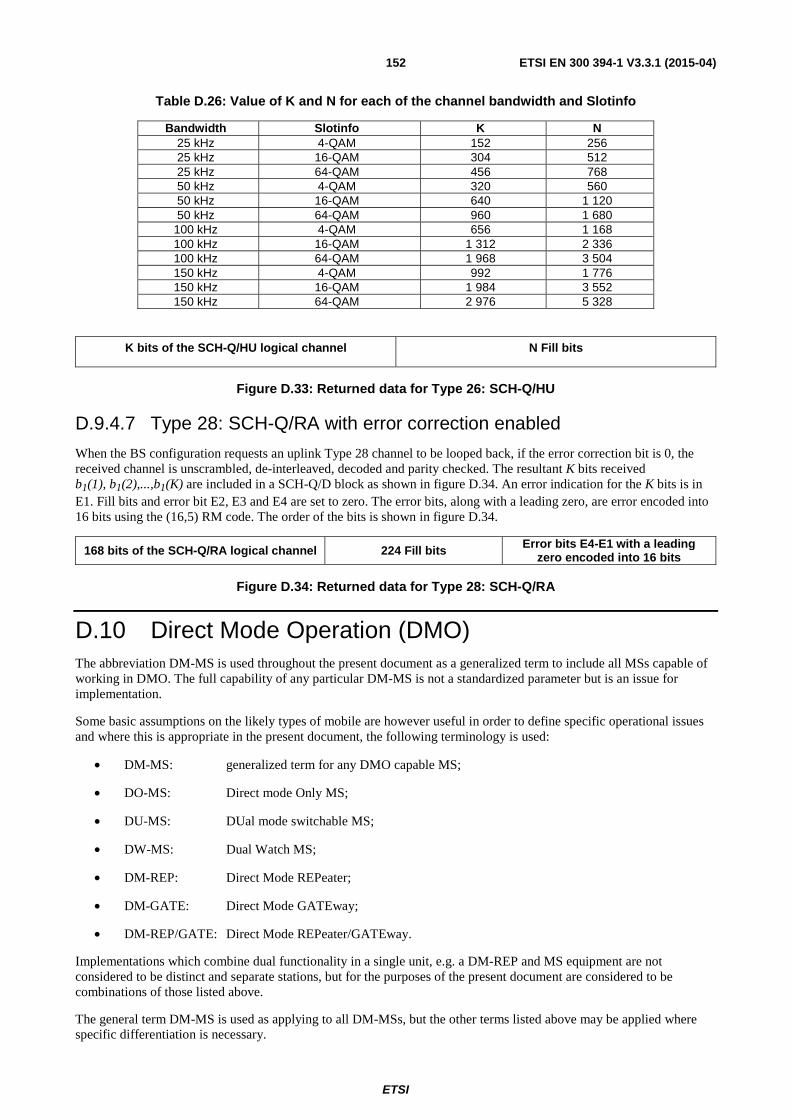
ETSI
ETSI EN 300 394-1 V3.3.1 (2015-04)152
Table D.26: Value of K and N for each of the channel bandwidth and Slotinfo
Bandwidth Slotinfo K N 25 kHz 4-QAM 152 256 25 kHz 16-QAM 304 512 25 kHz 64-QAM 456 768 50 kHz 4-QAM 320 560 50 kHz 16-QAM 640 1 120 50 kHz 64-QAM 960 1 680
100 kHz 4-QAM 656 1 168 100 kHz 16-QAM 1 312 2 336 100 kHz 64-QAM 1 968 3 504 150 kHz 4-QAM 992 1 776 150 kHz 16-QAM 1 984 3 552 150 kHz 64-QAM 2 976 5 328
K bits of the SCH-Q/HU logical channel N Fill bits
Figure D.33: Returned data for Type 26: SCH-Q/HU
D.9.4.7 Type 28: SCH-Q/RA with error correction enabled
When the BS configuration requests an uplink Type 28 channel to be looped back, if the error correction bit is 0, the received channel is unscrambled, de-interleaved, decoded and parity checked. The resultant K bits received b1(1), b1(2),...,b1(K) are included in a SCH-Q/D block as shown in figure D.34. An error indication for the K bits is in E1. Fill bits and error bit E2, E3 and E4 are set to zero. The error bits, along with a leading zero, are error encoded into 16 bits using the (16,5) RM code. The order of the bits is shown in figure D.34.
168 bits of the SCH-Q/RA logical channel 224 Fill bits Error bits E4-E1 with a leading zero encoded into 16 bits
Figure D.34: Returned data for Type 28: SCH-Q/RA
D.10 Direct Mode Operation (DMO) The abbreviation DM-MS is used throughout the present document as a generalized term to include all MSs capable of working in DMO. The full capability of any particular DM-MS is not a standardized parameter but is an issue for implementation.
Some basic assumptions on the likely types of mobile are however useful in order to define specific operational issues and where this is appropriate in the present document, the following terminology is used:
• DM-MS: generalized term for any DMO capable MS;
• DO-MS: Direct mode Only MS;
• DU-MS: DUal mode switchable MS;
• DW-MS: Dual Watch MS;
• DM-REP: Direct Mode REPeater;
• DM-GATE: Direct Mode GATEway;
• DM-REP/GATE: Direct Mode REPeater/GATEway.
Implementations which combine dual functionality in a single unit, e.g. a DM-REP and MS equipment are not considered to be distinct and separate stations, but for the purposes of the present document are considered to be combinations of those listed above.
The general term DM-MS is used as applying to all DM-MSs, but the other terms listed above may be applied where specific differentiation is necessary.
ETSI
ETSI EN 300 394-1 V3.3.1 (2015-04)153
D.10.1 Direct mode only mobile station (DO-MS) Continuous loop back in direct mode operation is not possible, because operation of traffic channels is in a true simplex mode, the same RF carrier and timeslot combination is used in both directions of a communication.
D.10.2 Dual mode switchable mobile station (DU-MS) Loop back testing can be performed with the mode switched to V+D. As it is unlikely that the RF circuitry will change when the mode is switched to DMO, only a functional test will be required in DMO mode.
D.10.3 Dual watch mobile station (DW-MS) Loop back testing can be performed with V+D operation activated. As it is unlikely that the RF circuitry will change when the DMO mode is active, only a functional test will be required for DMO operation.
D.10.4 Direct mode repeater (DM-REP) The operation of a DMO repeater is to forward the information from one Direct Mode MS (DM-MS) to another DM-MS, thus if the TSS transmit section acts as the sending DM-MS and the TSS receive section acts as the receiving DM-MS a natural loop back is formed and a test mode will only be required to override authentication and encryption procedures. For TCH/S BER testing it may be necessary to disable the repeater's normal Bad Frame Erasure operation.
D.10.5 Direct mode gateway (DM-GATE) The operation of a DMO gateway is to forward the information from a DM-MS to a SwMI (or vice versa), thus if the TSS transmitter acts as the sending DM-MS and the TSS receiver acts as the receiving BS (or vice versa) a natural loop back is formed. The test mode will only be required to indicate bad frames and bar authentication and encryption procedures.
D.10.6 Direct mode repeater/gateway combination (DM-REP/GATE)
The comments for DM-REP (clause D.10.4) and DM-GATE (clause D.10.5) shall apply.
D.10.7 DMO summary The specification is adequate in its present form for all types of DMO equipment with the exception of DO-MS. Special conditions applicable to using the T1 test mode with DO-MS equipment are defined in clauses F.4 and F.5 of the present document. DO-MS equipment cannot be tested using the TT test mode.
NOTE: At present, there is no DO-MS equipment in the market.
ETSI
ETSI EN 300 394-1 V3.3.1 (2015-04)154
Annex E (normative): Using RF loop back to test a TETRA MS Annex E applies to the TETRA Test (TT) Protocol Loopback method defined in clauses D.1 to D.6. Annex E does not apply to the T1 or T4 Loopback method defined in clauses D.7 and D.8.
E.1 Introduction The purpose of the RF loop back facility using the TT protocol is to provide a consistent method for assessing BER and MER on TETRA mobile stations, in production and service environments, without the need for special test connectors or adapters.
The present document is a guide to how the RF loop back facility may be used to test a TETRA MS. A simplified view of the test configuration during RF loop back testing is shown in figures E.1 and E.2.
Decoder, Channel extraction
PRBS generator
Frame Generator Coding etc .
Duplexer
PRBS Error detector
Part of TETRA System Simulator
Rx
Tx
Duplexer
Mobile on test
loop back
data for channel on test
test data
MS antenna connection
Figure E.1: RF Loop Back test configuration
Duplexer, Receiver, Transmitter
Demodulator
Modulator
Channel Decoder
Channel Encoder
Antenna
Selected channel at TMV-SAP
Figure E.2: Simplified diagram of MS during RF Loop Back
The message sequence and broadcast parameters used in the present document are intended as an illustration of one possible sequence of messages and set of parameters and defines how those shall be used, if that method is used. It is not intended to restrict the range of options used by mobile manufacturers. It is the responsibility of the TETRA System Simulator (TSS) designers to ensure that valid messages from the unit on test are correctly acknowledged and answered.
ETSI
ETSI EN 300 394-1 V3.3.1 (2015-04)155
E.2 Expected mode of operation for testing a MS To test a TETRA MS the TSS (acting as a base station) shall as a minimum generate in Downlink Continuous Transmission mode (D-CT) in a Normal Control mode (NC) with a Main Control Channel (MCCH) in time slot 1 of the main carrier.
A Broadcast Control Channel (BCCH) comprising a Broadcast Synchronization Channel (BSCH) and a Broadcast Network Channel (BNCH) shall be transmitted as a minimum to the requirements of ETSI EN 300 392-2 [1], clause 9.5.2.
Table E.1a: Example of use of TETRA frame structure for mobile testing
TN1 (CP) TN2 (UP) TN3 (UP or TP) TN4 (UP) MN1
FN1 to FN17
see note 1
SCH/HD (null) + SCH/HD (null)
or signalling + AACH
SCH/HD (null) + SCH/HD (null)
+ AACH
SCH/HD (null) + SCH/HD (null)
or TCH/x + AACH
SCH/HD (null) + SCH/HD (null)
+ AACH
MN1 FN18
SCH/HD (null) + SCH/HD (null) +
AACH
BSCH (sync info) + SCH/HD (null) + AACH (CLCH)
SCH/HD (null) + SCH/HD (null)
+ AACH
SCH/HD (null) + BNCH (sys info)
+ AACH MN2
FN1 to FN17
SCH/HD (null) + SCH/HD (null)
or signalling + AACH
SCH/HD (null) + SCH/HD (null)
+ AACH
SCH/HD (null) + SCH/HD (null)
or TCH/x + AACH
SCH/HD (null) + SCH/HD (null)
+ AACH
MN2 FN18
BSCH (syncinfo) + SCH/HD (null) +
AACH (CLCH)
SCH/HD (null) + SCH/HD (null)
+ AACH
SCH/HD (null) + BNCH (sys info)
+ AACH
SCH/HD (null) + SCH/HD (null)
+ AACH MN3
FN1 to FN17
SCH/HD (null) + SCH/HD (null)
or signalling + AACH
SCH/HD (null) + SCH/HD (null)
+ AACH
SCH/HD (null) + SCH/HD (null)
or TCH/x + AACH
SCH/HD (null) + SCH/HD (null)
+ AACH
MN3 FN18
SCH/HD (null) + SCH/HD (null) +
AACH
SCH/HD (null) + BNCH (sys info)
+ AACH
SCH/HD (null) + SCH/HD (null)
+ AACH
BSCH (sync info) + SCH/HD (null) + AACH (CLCH)
MN4 FN1 to FN17
SCH/HD (null) + SCH/HD (null)
or signalling + AACH
SCH/HD (null) + SCH/HD (null)
+ AACH
SCH/HD (null) + SCH/HD (null)
or TCH/x + AACH
SCH/HD (null) + SCH/HD (null)
+ AACH
MN4 FN18
SCH/HD (null) + BNCH (sys info) +
AACH
SCH/HD (null) + SCH/HD (null)
+ AACH
BSCH (sync info) + SCH/HD (null) + AACH (CLCH)
SCH/HD (null) + SCH/HD (null)
+ AACH NOTE 1: This structure of four multiframes MN1 ~ MN4 is repeated ×15 to form one Hyperframe, with the
Multiframe Number (MN) taking the values 1, 2, 3, 4, 5, 6, 7, 8, ..., 57, 58, 59, 60. NOTE 2: Mandatory mappings of BNCH, BSCH and opportunities for CLCH are shown in bold type.
An example of how the TSS structure might look is shown in table E.1a. Here a minimum requirement is shown; there is a single RF channel with MCCH on TN1. Signalling such as registration and call set up (and mobile initial access) will be on TN1. When a traffic channel is required (in this example) it will use TN3; TN2 and TN4 are not used and transmit null PDUs. (This is only one of many examples that could be described, but this example has the benefit of simplicity and single RF channel usage).
The Access Assignment Channel (AACH) shall allow sufficient opportunities for linearization and opportunities for a mobile to access the TSS.
Currently unallocated physical channels (UP) shall be filled with permitted logical control channels as indicated in ETSI EN 300 392-2 [1], clauses 9.5.2 and 9.5.3. In this simple example a SCH/HD containing a null PDU is used as follows in table E.1b.
ETSI
ETSI EN 300 394-1 V3.3.1 (2015-04)156
Table E.1b: Contents of SCH/HD when used as a fill signal
Parameter Bits Value Remarks NULL PDU PDU type 2 002 MAC_RESOURCE Fill bits 1 02 no fill bits Position of grant 1 02 do not care Encryption 2 002 No encryption Random Access Flag 1 02 Length 6 0000102 2 octets (null PDU) Address type 3 0002 Null PDU Fill 108 100 ... 02 1 + 107 0s
The contents of the TM_SDU(MLE_SYNC) and SYNC_PDU used for the BSCH are given in table E.2.
Table E.2: Contents of SYNC_PDU
Parameter Bits Value Remarks SYNC_PDU System code 4 00002 1st release V+D Base Colour Code 6 1 to 63 as required Timeslot number 2 current timeslot Frame number 5 current frame number Multiframe number 6 current MF number Sharing mode 2 002 continuous TX TS reserved frames 3 0002 do not care U-plane DTX 1 02 not allowed Frame 18 extension 1 02 no extension Reserved 1 02 default TM_SDU (D_MLE_SYNC) Mobile Country Code 10 00116 MCC = 001 for test Mobile Network Code 14 000116 MNC = 1 for test Neighbour cell broadcast D_NWRK_BROADCAST supported 1 02 not supported enquiry 1 02 not supported Cell service level 2 002 cell load unknown Late entry information 1 02 not supported
The contents of the TM_SDU (MLE_SYSINFO) and SYSINFO_PDU used for the BNCH are given in table E.3.
ETSI
ETSI EN 300 394-1 V3.3.1 (2015-04)157
Table E.3: Contents of SYSINFO PDU
Parameter Bits Value Remarks SYSINFO_PDU PDU type 2 102 Broadcast PDU Broadcast type 2 002 SYSINFO PDU Main carrier 12 as required Frequency band 4 as required Offset 2 002 0 kHz offset Duplex spacing 3 as required Reverse operation 1 as required No. of common 2ndry CCHs in use 2 002 none MS_TXPWR_MAX_CELL 3 0012 15 dBm default or as required RXLEV_ACCESS_MIN 4 00002 -125 dBm default or as required ACCESS_PARAMETER 4 00002 -53 dB default or as required RADIO_DOWNLINK_TIMEOUT 4 00002 disabled default or as required Hyperframe/CCK flag 1 02 hyperframe Hyperframe number 16 current HF number Optional field flag 2 102 access code A Default definition for access code A IMM (immediate) 4 11112 immediate access WT (waiting time) 4 as required Nu (access attempts) 4 as required Framelength factor 1 02 multiply by 1 Timeslot pointer 4 00002 same as downlink Minimum priority 3 0002 lowest priority (0) TM_SDU (MLE_SYSINFO) Location area 14 Any as required Subscriber class 16 FFFF16 all classes BS service details Registration 1 12 registration mandatory De-registration 1 12 de-registration mandatory Priority cell 1 12 priority cell Minimum mode service 1 0/12 as required Migration 1 12 supported Roaming 1 12 supported TETRA voice service 1 12 supported Circuit mode data service 1 12 supported CONP service 1 0/12 as required SCLNP service 1 0/12 as required Air interface encryption 1 02 not available Advanced link supported 1 0/12 as required
The Access Assignment Channel (AACH) during this initial period will allow access to all mobiles during Frames 1 to 17 on TN1, allow linearization on all Frame 18s containing a BSCH, and on other frames will mark the AACH as access reserved.
Initially, TN1 frames may be marked access reserved, to enable the TSS to control when the first access burst is sent, but this would need to be carefully handled to stop the TETRA equipment on test timing out because it had not confirmed the test mode setting.
As a minimum requirement, Access Code A is required, and in a test situation this will normally be the only Access Code used. Base frame length will be kept to a minimum to ensure fast test times. Initially, four AACH types are required; see tables E.4 to E.7. Once messages are exchanged, other AACH values will be required.
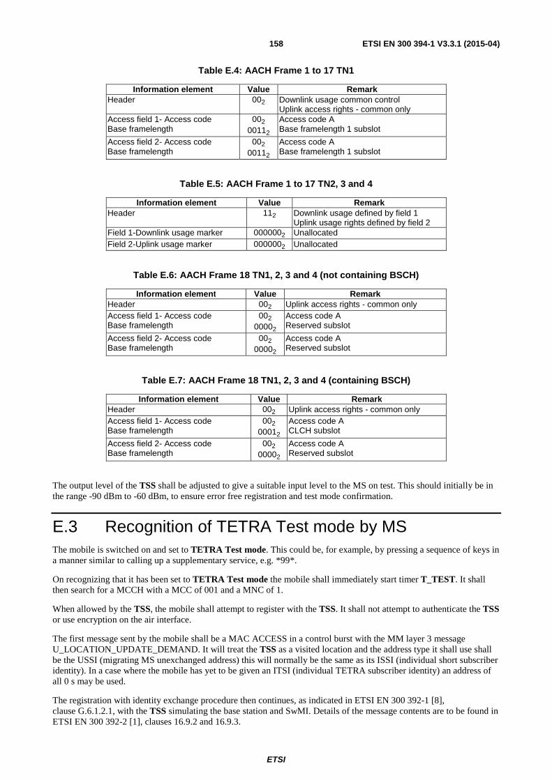
ETSI
ETSI EN 300 394-1 V3.3.1 (2015-04)158
Table E.4: AACH Frame 1 to 17 TN1
Information element Value Remark Header 002 Downlink usage common control
Uplink access rights - common only Access field 1- Access code Base framelength
002 00112
Access code A Base framelength 1 subslot
Access field 2- Access code Base framelength
002 00112
Access code A Base framelength 1 subslot
Table E.5: AACH Frame 1 to 17 TN2, 3 and 4
Information element Value Remark Header 112 Downlink usage defined by field 1
Uplink usage rights defined by field 2 Field 1-Downlink usage marker 0000002 Unallocated Field 2-Uplink usage marker 0000002 Unallocated
Table E.6: AACH Frame 18 TN1, 2, 3 and 4 (not containing BSCH)
Information element Value Remark Header 002 Uplink access rights - common only Access field 1- Access code Base framelength
002 00002
Access code A Reserved subslot
Access field 2- Access code Base framelength
002 00002
Access code A Reserved subslot
Table E.7: AACH Frame 18 TN1, 2, 3 and 4 (containing BSCH)
Information element Value Remark Header 002 Uplink access rights - common only Access field 1- Access code Base framelength
002 00012
Access code A CLCH subslot
Access field 2- Access code Base framelength
002 00002
Access code A Reserved subslot
The output level of the TSS shall be adjusted to give a suitable input level to the MS on test. This should initially be in the range -90 dBm to -60 dBm, to ensure error free registration and test mode confirmation.
E.3 Recognition of TETRA Test mode by MS The mobile is switched on and set to TETRA Test mode. This could be, for example, by pressing a sequence of keys in a manner similar to calling up a supplementary service, e.g. *99*.
On recognizing that it has been set to TETRA Test mode the mobile shall immediately start timer T_TEST. It shall then search for a MCCH with a MCC of 001 and a MNC of 1.
When allowed by the TSS, the mobile shall attempt to register with the TSS. It shall not attempt to authenticate the TSS or use encryption on the air interface.
The first message sent by the mobile shall be a MAC ACCESS in a control burst with the MM layer 3 message U_LOCATION_UPDATE_DEMAND. It will treat the TSS as a visited location and the address type it shall use shall be the USSI (migrating MS unexchanged address) this will normally be the same as its ISSI (individual short subscriber identity). In a case where the mobile has yet to be given an ITSI (individual TETRA subscriber identity) an address of all 0 s may be used.
The registration with identity exchange procedure then continues, as indicated in ETSI EN 300 392-1 [8], clause G.6.1.2.1, with the TSS simulating the base station and SwMI. Details of the message contents are to be found in ETSI EN 300 392-2 [1], clauses 16.9.2 and 16.9.3.

ETSI
ETSI EN 300 394-1 V3.3.1 (2015-04)159
The procedure is successfully completed when the TSS has sent a D_LOCATION_UPDATE_ACCEPT message which the mobile has acknowledged. The TSS shall then send a TT layer 3 message D_TEST_MODE_CONFIRM_COMMAND which the mobile acknowledges with a TEST_MODE_CONFIRM message. At this point the mobile shall stop timer T_TEST and go into the test mode operating state.
During this procedure the TSS will use the MAC_RESOURCE header and modify the AACH to reserve subslots to allow the mobile to transmit, and indicate when messages are being sent to the mobile. The use of the AACH shall be as given in the TETRA specification ETSI EN 300 392-2 [1], clause 21.4.7.
In TETRA Test mode the MS shall accept and generate all normal valid commands, with the exception of some Mobility Management (MM) commands and with the addition of commands with the TT protocol discriminator, some of the exceptions being:
• it shall not action a D_DISABLE command neither temporary nor permanent;
• it shall not encrypt messages on the air interface;
• it shall not attempt to authenticate the TSS.
The full list of exceptions is given in clause D.3.2.1.
If the timer T_TEST expires before the above procedure is completed then the mobile shall revert to normal operational mode i.e. start searching for a control channel allowed by its subscription parameters. To retry to set into test mode would require the user to set test mode again, i.e. in the example the key sequence *99* would need entering again.
With the test mode confirmed the mobile shall be in the idle and registered state listening for paging messages etc. It shall also have the ability to place and answer calls. If the MS has any kind of visual display, it should indicate that it is set in test mode. This could be for example by displaying the word "TEST" in the display panel, or for a MS with no display panel this could be by flashing an indicator light in a particular manner.
E.4 Using loop back to test traffic channels To test a mobile on a traffic channel, for example to perform a BER test, requires that an individual call be in progress and then a RF loop back invoked. The call can be placed from the TSS or the mobile.
Where the mobile has duplex capability, the call shall be set up in duplex mode. To maintain the channel during a simplex call, message trunking is used. Message trunking is indicated by the MAC_RESOURCE PDU at an "over" when the PDU does not have a channel allocation returning the mobile back to the MCCH. In the simple scenario described the traffic channel will be allocated to TN3 on the main carrier.
To invoke the loop back a D_LOOP_COMMAND message is sent to the mobile, this shall indicate that the (current) traffic channel is to be looped back. The message may indicate in the "loopback type" element that BFI (bad frame indication) is to be used; this only applies to a speech traffic channel and the "loopback type" element should be ignored for data traffic channels. The mobile shall respond with a U_LOOP_CONFIRM message. The mobile shall also loop the received traffic channel to the transmitter as indicated in the main text of the present document. During loop back the traffic channel received is decoded to type-1 bits at the TMV-SAP level and then the type-1 bits are re-encoded and returned on an identical traffic channel to the TSS.
3 examples are outlined below:
• TCH/7,2;
• TCH/S;
• TCH/2,4 with N = 8.
During the call the TSS shall use normal procedures on the AACH, this shall normally involve allocating a usage marker to the call and marking, via the AACH, the uplink and downlink slots to be used with the usage marker.
During loop back the uplink and downlink slots shall be marked for use as a traffic channel, via the AACH. In the example considered the AACH will mark all TN3 slots, both uplink and downlink, of the main carrier in frames 1 to 17 with the usage marker allocated for the call.
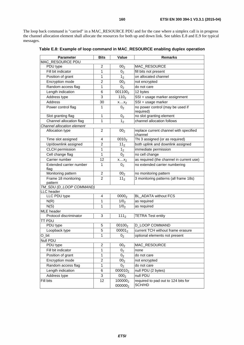
ETSI
ETSI EN 300 394-1 V3.3.1 (2015-04)160
The loop back command is "carried" in a MAC_RESOURCE PDU and for the case where a simplex call is in progress the channel allocation element shall allocate the resources for both up and down link. See tables E.8 and E.9 for typical messages.
Table E.8: Example of loop command in MAC_RESOURCE enabling duplex operation
Parameter Bits Value Remarks MAC_RESOURCE PDU PDU type 2 002 MAC_RESOURCE Fill bit indicator 1 02 fill bits not present Position of grant 1 12 on allocated channel Encryption mode 2 002 not encrypted Random access flag 1 02 do not care Length indication 6 0011002 12 bytes Address type 3 1102 SSI + usage marker assignment Address 30 x....x2 SSI + usage marker Power control flag 1 02 no power control (may be used if
required) Slot granting flag 1 02 no slot granting element Channel allocation flag 1 12 channel allocation follows Channel allocation element Allocation type 2 002 replace current channel with specified
channel Time slot assigned 4 00102 TN 3 assigned (or as required) Up/downlink assigned 2 112 both uplink and downlink assigned CLCH permission 1 12 immediate permission Cell change flag 1 02 no cell change Carrier number 12 x....x2 as required (the channel in current use) Extended carrier number flag
1 02 no extended carrier numbering
Monitoring pattern 2 002 no monitoring pattern Frame 18 monitoring pattern
2 112 3 monitoring patterns (all frame 18s)
TM_SDU (D_LOOP COMMAND) LLC header LLC PDU type 4 00002 BL_ADATA without FCS N(R) 1 1/02 as required N(S) 1 1/02 as required MLE header Protocol discriminator 3 1112 TETRA Test entity TT PDU PDU type 5 001002 D_LOOP COMMAND Loopback type 5 000012 current TCH without frame erasure O_bit 1 02 optional elements not present Null PDU PDU type 2 002 MAC_RESOURCE Fill bit indicator 1 02 none Position of grant 1 02 do not care Encryption mode 2 002 not encrypted Random access flag 1 02 do not care Length indication 6 0000102 null PDU (2 bytes) Address type 3 0002 null PDU Fill bits 12 1000002
0000002 required to pad out to 124 bits for SCH/HD
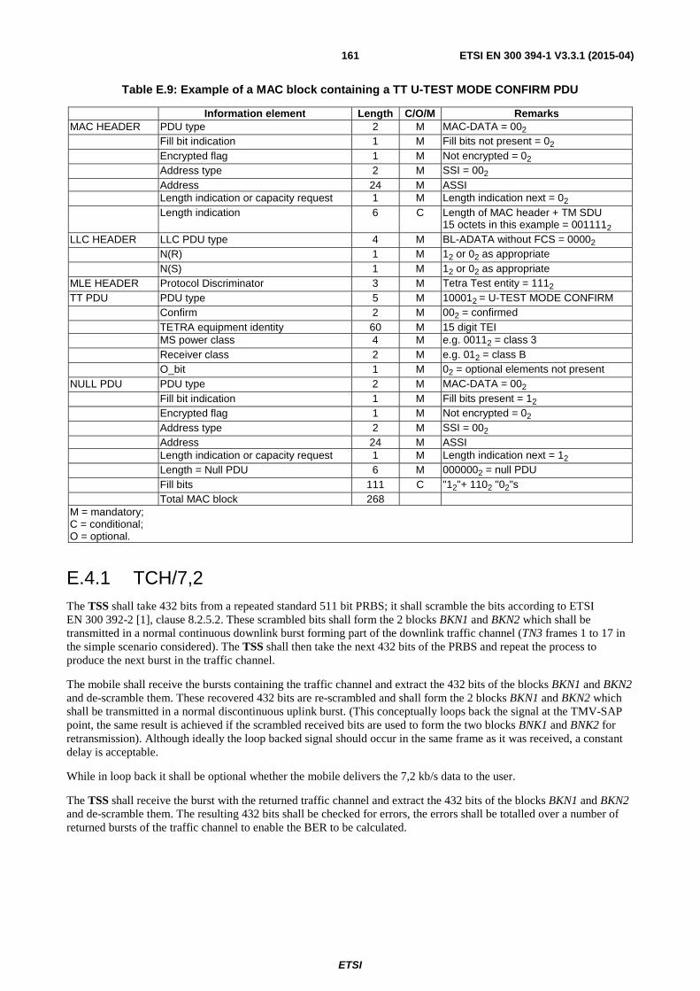
ETSI
ETSI EN 300 394-1 V3.3.1 (2015-04)161
Table E.9: Example of a MAC block containing a TT U-TEST MODE CONFIRM PDU
Information element Length C/O/M Remarks MAC HEADER PDU type 2 M MAC-DATA = 002 Fill bit indication 1 M Fill bits not present = 02 Encrypted flag 1 M Not encrypted = 02 Address type 2 M SSI = 002 Address 24 M ASSI Length indication or capacity request 1 M Length indication next = 02 Length indication 6 C Length of MAC header + TM SDU
15 octets in this example = 0011112 LLC HEADER LLC PDU type 4 M BL-ADATA without FCS = 00002 N(R) 1 M 12 or 02 as appropriate N(S) 1 M 12 or 02 as appropriate MLE HEADER Protocol Discriminator 3 M Tetra Test entity = 1112 TT PDU PDU type 5 M 100012 = U-TEST MODE CONFIRM Confirm 2 M 002 = confirmed TETRA equipment identity 60 M 15 digit TEI MS power class 4 M e.g. 00112 = class 3 Receiver class 2 M e.g. 012 = class B O_bit 1 M 02 = optional elements not present NULL PDU PDU type 2 M MAC-DATA = 002 Fill bit indication 1 M Fill bits present = 12 Encrypted flag 1 M Not encrypted = 02 Address type 2 M SSI = 002 Address 24 M ASSI Length indication or capacity request 1 M Length indication next = 12 Length = Null PDU 6 M 0000002 = null PDU Fill bits 111 C "12"+ 1102 "02"s Total MAC block 268 M = mandatory; C = conditional; O = optional.
E.4.1 TCH/7,2 The TSS shall take 432 bits from a repeated standard 511 bit PRBS; it shall scramble the bits according to ETSI EN 300 392-2 [1], clause 8.2.5.2. These scrambled bits shall form the 2 blocks BKN1 and BKN2 which shall be transmitted in a normal continuous downlink burst forming part of the downlink traffic channel (TN3 frames 1 to 17 in the simple scenario considered). The TSS shall then take the next 432 bits of the PRBS and repeat the process to produce the next burst in the traffic channel.
The mobile shall receive the bursts containing the traffic channel and extract the 432 bits of the blocks BKN1 and BKN2 and de-scramble them. These recovered 432 bits are re-scrambled and shall form the 2 blocks BKN1 and BKN2 which shall be transmitted in a normal discontinuous uplink burst. (This conceptually loops back the signal at the TMV-SAP point, the same result is achieved if the scrambled received bits are used to form the two blocks BNK1 and BNK2 for retransmission). Although ideally the loop backed signal should occur in the same frame as it was received, a constant delay is acceptable.
While in loop back it shall be optional whether the mobile delivers the 7,2 kb/s data to the user.
The TSS shall receive the burst with the returned traffic channel and extract the 432 bits of the blocks BKN1 and BKN2 and de-scramble them. The resulting 432 bits shall be checked for errors, the errors shall be totalled over a number of returned bursts of the traffic channel to enable the BER to be calculated.
ETSI
ETSI EN 300 394-1 V3.3.1 (2015-04)162
E.4.2 TCH/S The TSS shall take 2 contiguous samples of 137 bits from a repeated standard 511 bit PRBS, these shall represent 2 frames from a speech encoder. Sample 1 forms the Type-1 bits A1 to A137, sample 2 forms the Type-1 bits B1 to B137. The bits are then reordered, parity and tail bits added, convolution coding applied, interleaved and finally scrambled (naming and numbering notation and coding procedure is that used in ETSI EN 300 395-2 [12], clause 5). The 432 scrambled bits shall form the 2 blocks BKN1 and BKN2 which shall be transmitted in a normal continuous downlink burst forming part of the downlink traffic channel (TN3 frames 1 to 17 in the simple scenario considered). The TSS shall then take the next 2 contiguous samples of 137 bits of the PRBS and repeat the process to produce the next burst in the traffic channel.
The mobile shall receive the bursts containing the traffic channel and extract the 432 bits of the blocks BKN1 and BKN2 and decode them. The result after de-scrambling, de-interleaving and de-convolution shall be 286 type-2 bits. The 60 class 2 bits shall have their parity bits calculated and checked against the received parity bits. If the parity bits do not match then this shall be an indication of a bad frame for when this is required. The type-1 bits shall be extracted from the type-2 bits. The resulting 2 speech frames are used as the inputs to the encoding process (This conceptually loops back the signal at the TMV-SAP point, the same result is achieved if the type-2 bits are looped back with parity bits recalculated). The speech frames are encoded and the resulting 432 bits shall form the 2 blocks BKN1 and BKN2 which shall be transmitted in a normal discontinuous uplink burst. Although ideally the looped back signal should occur in the same frame as it was received, a constant delay is acceptable.
In the case where the D_LOOP_COMMAND message has requested BFI the return signal may be modified. If the parity check on the class 2 bits fail or some other indication of an unusable traffic sample is indicated by the mobile and BFI is requested then the two return samples should be set to all 1s prior to encoding for retransmission.
While in loop back it shall be optional whether the mobile delivers "speech" to the user. (It is probably advisable not to "deliver" the speech to avoid uncomfortable noises to any listener).
The TSS shall receive the burst with the returned traffic channel and extract the 432 bits of the blocks BKN1 and BKN2 and decode them. The resulting two 137 bit speech frames shall be checked for errors; the errors shall be totalled over a number of returned bursts of the traffic channel to enable the BER to be calculated. Where BFI has been requested the TSS shall recognize the samples set to all "1"s as bad frames, calculating the BER only in those frames which do not indicate BFI.
E.4.3 TCH/2,4, N = 8 The TSS shall take 144 bits from a repeated standard 511 bit PRBS, it shall add 4 tail bits and RCPC (convolution) code with r = 148/432. The resultant 432 bit type-3 bits are interleaved over 8 blocks. A completed block shall contain an equal number of convoluted bits from 8 samples of the PRBS. Each completed block of 432 bits is further interleaved to form the type-4 bits which shall then be scrambled (these processes are according to ETSI EN 300 392-2 [1], clause 8). These scrambled bits shall form the 2 blocks BKN1 and BKN2 which shall be transmitted in a normal continuous downlink burst forming part of the downlink traffic channel (TN3 frames 1 to 17 in the simple scenario considered). The TSS shall continue taking contiguous 144 bit samples of the PRBS and repeat the processes described.
The mobile shall receive the bursts containing the traffic channel and extract the 432 bits of the blocks BKN1 and BKN2 and de-scramble them. The bits shall be block de-interleaved. Then the information shall be further de-interleaved over the 8 blocks originally contributing to the block. When an originating block is completed it shall be de-convoluted and the tail bits removed to obtain the 144 data bits. The recovered data along with other retrieved samples shall then be re-encoded as described for the TSS for retransmission. (This conceptually loops back the signal at the TMV-SAP point).
While in loop back it shall be optional whether the mobile delivers the 2,4 kb/s data to the user.
The TSS shall receive the burst with the returned traffic channel and extract the 432 bits of the blocks BKN1 and BKN2 and de-scramble them etc. The resulting 144 type-1 bits shall be checked for errors, the errors shall be totalled over a number of returned bursts of the traffic channel to enable the BER to be calculated. Interleaving over 8 blocks causes an overall delay of at least 16 frames between the original sample and the received sample for checking. The delay may be longer but shall be constant.
ETSI
ETSI EN 300 394-1 V3.3.1 (2015-04)163
E.4.4 Control messages during loop back of traffic channels During the period in which error tests are in progress, there shall normally be no control messages sent. If however the TSS requires to send a control message, for example to request a change in power level, the burst containing the message will have training sequence number 2 indicating channel stealing (STCH). The mobile shall decode and action the message, it may stop, temporarily, the loop back mechanism until the signalling sequence is completed i.e. the message has been acknowledged or answered. It is the responsibility of the TSS to allow for this interruption in any error counting procedure, etc.
If during the loop back the mobile transmits a control message, for example an attempt to invoke a supplementary service is made, the TSS shall acknowledge the message and may indicate to the test operator via the TSS MMI that an unexpected interruption has occurred. Whether the test in progress is terminated, repeated or continued depends on the type of interruption and is a matter for the designer of the TSS.
ETSI
ETSI EN 300 394-1 V3.3.1 (2015-04)164
Annex F (normative): Direct Mode (DM) Conformance Testing
F.1 Scope Annex F defines the test limits and measurement methods to be used for the conformance testing of radio aspects of TETRA terminals which are capable of operating in Direct Mode Operation (DMO). It applies to the following types of Direct Mode terminal:
• DO-MS,
• DU-MS,
• DW-MS,
• DM-REP,
• DM-GATE,
• DM-REP/GATE.
F.2 Definitions, symbols and abbreviations Refer to ETSI EN 300 396-1 [i.2] and ETSI EN 300 396-2 [7], clause 3.1 for common definitions.
F.3 General With the exception of DO-MS equipment, all equipment which is capable of DMO is also capable of TETRA trunked mode V+D operation, and therefore has to pass the radio aspects conformance tests in the present document. DO-MS equipment is required by ETSI EN 300 396-2 [7] to fulfil most of the radio requirements of trunked mode Class B V+D MS equipment, the main exceptions being power control and reception of the AACH logical channel. Therefore, this annex requires all equipment which is capable of DMO to meet the present document, with certain exceptions for DO-MS equipment.
NOTE: For DM-MS equipment which is designed specifically as DO-MS (rather than being a DU-MS with the V+D operation disabled in software), it is possible that this equipment will not be physically capable of operating in the frequency duplex mode required to conduct tests under clauses 8 to 10.
Equipment which is capable of DMO is required by ETSI EN 300 396-2 [7] to meet slightly more stringent test limits for transmitter output power below maximum power class. Therefore, this annex requires all equipment which is capable of DMO to meet the present document using the more stringent limits where applicable.
Direct Mode Operation involves two radio aspects which are not covered by the present document, unsynchronized transmission and direct mode burst profiles. Therefore, this annex requires all equipment which is capable of DMO to provide an additional DMO Test Transmit Mode, and to meet the requirements of two additional tests.
F.4 Radio test modes For the purpose of testing, all equipment which is capable of DMO shall provide test modes which enable all of the MS V+D tests in clauses 8 to 10 to be performed as specified (see note in table F.1), except as shown in table F.1, and shall also provide a DMO test transmit mode as defined in clause F.6.1.

ETSI
ETSI EN 300 394-1 V3.3.1 (2015-04)165
Table F.1: Test Case Exceptions for equipment capable of Direct Mode Operation
Clause Equipment Type Test Case Exception 8.1.1.1 a) DO-MS
(one power class) The DO-MS shall disregard the T1 level, Access_parameter and MS_TXPWR_MAX_CELL parameters, and shall set its transmitter output power to its nominal power class.
8.1.1.1 a) DO-MS (more than one power class)
The DO-MS shall either set its power according to test case 1 or shall be switched to its highest power class.
8.1.1.1 b) DO-MS (one power class)
The test shall not be repeated for test cases 2 to 7.
8.1.1.1 b) DO-MS (more than one power class)
All of the other power classes shall be tested by the DO-MS either setting its power according to test cases 2 to 7 as appropriate, or by being switched to its other power classes.
8.3 DO-MS (one power class)
The test shall not be repeated for test case 7.
8.3 DO-MS (more than one power class)
The test shall be repeated by the DO-MS either setting its lowest power class in response to test case 7 or by being switched to its lowest power class.
10.5 DO-MS This test shall not be performed. NOTE: The T1 signal supplied shall be identical to the normal T1 signal used for V+D testing. FN18 will
contain BSCH (not SCH/S) scrambled with all-zeroes scrambling code, and BNCH/T (not SCH/H) scrambled with the normal extended colour code obtained from the BSCH (not all zeroes scrambling code). The bursts transmitted by the DM-MS in this test mode shall be Normal Uplink Bursts or Control Bursts as indicated in the BNCH/T information (not the Direct Normal Burst and Direct Synchronization Burst).
F.5 Test conditions All equipment which is capable of DMO shall be tested according to clauses 8, 9, 10 and 11, except as shown in table F.1, and shall meet the test limits defined in clause 7, except as shown in table F.2.
Table F.2: Test limit exceptions for equipment capable of Direct Mode Operation
Clause Equipment Type Test Limit Exception 7.1.1.2 All types The limits for the MS power class (specified in ETSI EN 300 396-2 [7],
clause 6) apply to all power levels tested which correspond to power classes of the equipment.
7.1.5.2 All types See note 1. 7.2.2.2 DO-MS Table A.2 applies (as MS receiver V+D Class B, see note 2). 7.2.3.2 DO-MS Table A.2 and table A.6 apply (as MS receiver V+D Class B, see note 2),
but with no requirement to measure AACH. 7.2.4.2 DO-MS Table A.2 applies (as MS receiver V+D Class B, see note 2). 7.2.5.2 DO-MS Table A.2 applies (as MS receiver V+D Class B). 7.2.6.2 DO-MS Table A.2 applies (as MS receiver V+D Class B). 7.2.7.2 DO-MS Table A.2 applies (as MS receiver V+D Class B).
NOTE 1: In the case where a DM-MS transmits on a DM channel frequency which is within its normal V+D MS Tx band, then the limits shall apply symmetrically to both sides of the MS Tx band, where frb denotes the frequency offset corresponding to the near edge of the received band or 5 MHz (10 MHz for frequencies above 520 MHz) whichever is greater. All levels are expressed in dBc relative to the actual transmitted power level, and in any case no limit tighter than -55 dBm for offsets ≤ frb or -70 dBm for offsets > frb shall apply.
In other cases, the -100 dBc requirement shall apply outside of the frequency range fx which comprises the range of frequencies over which the equipment is able to transmit within the TETRA standard, plus a guard band of 5 MHz on either side as shown in ETSI EN 300 396-2 [7], figure 6. In any case no limit tighter than -70 dBm shall apply.
NOTE 2: Where propagation condition TU50 is specified in tables A.2 and A.6 the test shall be performed using propagation condition DR50 defined in ETSI EN 300 396-2 [7], clause 6.

ETSI
ETSI EN 300 394-1 V3.3.1 (2015-04)166
F.6 Additional tests for equipment which is capable of Direct Mode Operation
F.6.1 DMO test transmit mode The manufacturer shall provide the means to operate the equipment under test in DMO test transmit mode over the frequency range which includes at least the declared DMO RF carrier frequency range. DMO test transmit mode shall be selected using the method provided by the manufacturer.
In DMO test transmit mode, the equipment under test shall be configured to transmit a signal as follows. In timeslot 1 of frame 18, a Direct Synchronization Burst (DSB) containing SCH/S and SCH/H information shall be transmitted. In timeslot 1 of frames 1 to 17, a Direct Normal Burst (DNB) containing channel type 1 (TCH/7,2) information shall be transmitted. In timeslots 2 to 4 of frames 1 to 18, nothing shall be transmitted, except that the equipment may transmit a DSB in timeslot 3 of frames 6, 12 and 18, and a linearization burst in timeslot 3 of frame 3. This sequence may be preceded by continuous DSB transmission. A bit stream, produced by repeating a pseudo random sequence with a length of 511 bits according to Recommendation ITU-T O.153 [2], shall be used as the information to be transmitted over the TCH/7,2 logical channel.
The equipment shall set its transmit power according to its DMO power class, specified in ETSI EN 300 396-2 [7], clause 6. If the equipment has more than one DMO power class, the highest power class shall be selected using the method provided by the manufacturer.
In DMO test transmit mode, the equipment under test is not provided with a test signal from the test system, and derives its frequency and timing information from its own internal frequency reference.
F.6.2 DMO transmitter output power profile
F.6.2.1 DMO transmitter output power profile, limit values
The following requirement shall be met.
The transmitter output power versus time shall be within the power time mask specified in ETSI EN 300 396-2 [7], clause 6, figure 7, measured through the TETRA filter, refer to B.1.2.2, under normal test conditions. The time periods t1, t2 and t3 in ETSI EN 300 396-2 [7], clause 6, figure 7 are defined in ETSI EN 300 396-2 [7], clause 6, table 6.
F.6.2.2 DMO transmitter output power profile, method of measurement
This test shall be performed under normal test conditions specified in clause 6, on the middle radio frequency channel in the band in which the equipment is intended for DMO.
a) The DMO equipment shall be connected to the test system, and shall be placed in DMO test transmit mode on its highest DMO power class.
b) The sampling system shall capture a representation of the DMO transmit burst's amplitude and timing (excluding any LCH transmissions). The procedure shall be repeated for 200 bursts and the test system shall calculate the following two parameters:
b1) the average power versus time profile during time periods t1 and t3 (figure 7 in ETSI EN 300 396-2 [7]),
extended at least 5 symbol periods before the start of t1 and at least 5 symbol periods after the end of t3,
sampled at a rate equal to or greater than the symbol rate, where each point represents the average power per sample, as estimated from the 200 arrays;
b2) the average power over the useful part of a burst (the modulation symbol times SN0 to SNmax defined in ETSI EN 300 396-2 [7], clause 9), sampled at symbol rate at symbol time, further averaged over the 200 burst measurements. This single power value shall be used as the 0 dB reference for the power versus time profile determined in step b1) above.
ETSI
ETSI EN 300 394-1 V3.3.1 (2015-04)167
F.6.3 DMO Carrier frequency accuracy
F.6.3.1 DMO Carrier frequency accuracy, limit values
The carrier frequency error in any burst shall be within ±1,0 kHz measured under normal and extreme test conditions.
F.6.3.2 DMO Carrier frequency accuracy, method of measurement
This test shall be performed under normal and extreme test conditions specified in clause 6, on the middle radio frequency channel in the band in which the equipment is intended for DMO. The measurement described here is performed on direct mode normal bursts, defined in ETSI EN 300 396-2 [7], clause 9. The sampling system in annex B, clause B.1.2 shall be employed.
a) The DMO equipment shall be connected to the test system, and shall be placed in DMO test transmit mode on its highest DMO power class.
b) The sampling system shall capture a representation of the DMO transmit burst's modulation symbol Z(k) at sampling times tk (symbol by symbol) where tk is the symbol time corresponding to the kth symbol. For each
symbol the sampling system shall measure the phase rotation θ which is caused by the frequency difference between the DMO equipment and the sampling system, as defined in ETSI EN 300 396-2 [7], clause 6. The sampling system shall calculate the frequency error df for the burst as follows:
df = 1/(2π T SNmax) θ(k)
where df is expressed in Hz, T is the symbol duration in seconds, θ(k) is expressed in radians, and SNmax is the number of symbols in a burst, defined in ETSI EN 300 396-2 [7], clause 9.
c) The procedure described in step b) shall be repeated for 20 bursts.
F.6.4 DM-MS Slave synchronization accuracy
F.6.4.1 DM-MS Slave synchronization accuracy, definition
DM-MS slave synchronization accuracy (error) is defined as a difference between the actual transmitted carrier frequency and the nominal synchronized carrier frequency, where the nominal synchronized carrier frequency is defined as the nominal transmit carrier frequency subject to the same frequency variation as the carrier frequency of the signal received by the DM-MS.
NOTE: When the DM-MS equipment is required to transmit in slave mode, it is important that it synchronizes with and transmits back to the master on the master's frequency and timing. This happens, for example, during pre-emption request, changeover request (when the channel is reserved), timing change request, responding to call set-up with presence check and when responding to acknowledged short data message.
F.6.4.2 DM-MS Slave synchronization accuracy, limit values
The DM-MS slave synchronization accuracy in any burst shall be within ±100 Hz, measured under normal test conditions.
F.6.4.3 DM-MS Slave synchronization accuracy, method of measurement
a) The test system shall transmit test signal T1 at a carrier frequency which is varied by +1,0 kHz from the nominal carrier frequency, using a frequency reference for the timebase used to generate the modulation symbols which is varied by +2,0 ppm.
b) The test defined in clause 10.2.1 shall be performed using the T1 signal subject to frequency variation as defined in step a).
c) Steps a) and b) shall be repeated with a carrier frequency variation of -1,0 kHz and a timebase frequency reference variation of -2,0 ppm.
k
SN
=∑
1
max
ETSI
ETSI EN 300 394-1 V3.3.1 (2015-04)168
Annex G (informative): Change requests The present document includes change requests as presented in table G.1.
Table G.1: Change requests
No CR vers.
Standard Version
Clauses affected Title CR Status
001 V2.3.1 2, 7.1.1.2, 7.1.2.1, 8.1.1, 8.1.2, 9.6, C.3.1
Update of table and figure references to ETSI EN 300 392-2 [1] and other editorial updates
Approved
401 11 V3.1.1 2, 2.1, 2.2, 5.3.5.1.1, 10.2.1, 10.2.2, 10.2.3, 10.2.4, C.5.1, E.3
Editorial correction WG3 approved 080624
402 10 V3.1.1 7.1.1.2, 7.1.2.1, 8.1.1.1 Air to ground requirements WG3 approved 080624
403 10 V3.1.1 7.2.4.3.1, A.2 TEDS ACR values WG3 approved 090903
404 10 V3.1.1 Annex C TEDS TTCI WG3 approved 090401
405 11 V3.1.1 A.2 Clause A.2 tables WG3 approved 090401
406 10 V3.1.1 3.3, D.10, F.1, F2, F.3, F.4, F.5, F.6
Update DMO test clauses regarding latest published DMO standards
WG3 approved 090507
407 05 V3.1.1 5.2.1, A.3 BNCH/T definition and testing of TEDS header logical channels
408 10 V3.1.1 A.2 Question marks in the table A.13 WG3 approved 090903
409 20 V3.2.1 5.3.5.1 Correction in T4 signal references in 5.3.5.1 WG3 approved 17.06.2014
ETSI
ETSI EN 300 394-1 V3.3.1 (2015-04)169
History
Document history
Edition 1 March 1996 Publication as ETSI ETS 300 394-1 (Historical)
V2.1.1 September 2000 Publication as ETSI TS 100 394-1
V2.2.1 September 2000 Publication as ETSI TS 100 394-1 (Withdrawn)
V2.1.2 December 2000 Publication
V2.3.1 December 2000 Publication as ETSI TS 100 394-1
V2.3.1 April 2001 Publication
V2.4.1 February 2006 Publication
V3.1.1 November 2007 Publication
V3.2.1 October 2012 Publication
V3.3.0 December 2014 EN Approval Procedure AP 20150415: 2014-12-16 to 2015-04-15
V3.3.1 April 2015 Publication