erk jensen, cern be-rf
TRANSCRIPT

CERN Accelerator School, Divonne 2009
Erk Jensen, CERN BE-RF

CERN Accelerator School, Divonne 2009
dB
t-domain vs. ω-domain
phasors
2RF I24 February, 2009

CERN Accelerator School, Divonne 2009
Convenient logarithmic measure of a power ratio.
A “Bel” (= 10 dB) is defined as a power ratio of 101. Consequently, 1 dB is a power ratio of 100.1≈1.259
If rdb denotes the measure in dB, we have:
Related: dBm (relative to 1 mW), dBc (relative to carrier)
rdb -30 dB -20 dB -10 dB -6 dB -3 dB 0 dB 3 dB 6 dB 10 dB 20 dB 30 dB
P2/P1 0.001 0.01 0.1 0.25 .50 1 2 3.98 10 100 1000
A2/A1 0.0316 0.1 0.316 0.50 .71 1 1.41 2 3.16 10 31.6
3RF I24 February, 2009

CERN Accelerator School, Divonne 2009
An arbitrary signal g(t) can be expressed in ω-domain using the Fourier transform (FT).
The inverse transform (IFT)is also referred to asFourier Integral
The advantage of the ω-domain description is that linear time-invariant (LTI) systems are much easier described.
The mathematics of the FT requires the extension of the definition of a function to allow for infinite values and non-converging integrals.
The FT of the signal can be understood at looking at “what frequency components it’s composed of”.
4RF I24 February, 2009

CERN Accelerator School, Divonne 2009
For T-periodic signals, the FT becomes the Fourier-Series, dω becomes , ∫ becomes Σ.
The cousin of the FT is the Laplace transform, which uses a complex variable (often s) instead of jω; it has generally a better convergence behaviour.
Numerical implementations of the FT require discretisation in t (sampling) and in ω. There exist very effective algorithms (FFT).
In digital signal processing, one often uses the related z-Transform, which uses the variable , where τis the sampling period. A delay of kτ becomes z-k.
5RF I24 February, 2009

CERN Accelerator School, Divonne 2009
General:
This can be interpreted as the projection on the real axis of a circular motion in the complex plane.
The complex amplitudeis called “phasor”.
real part
imag
inar
y p
artω
6RF I24 February, 2009

CERN Accelerator School, Divonne 2009
Why this seeming “complication”?:Because things become easier!
Using , one may now forget about the rotation with ωand the projection on the real axis, and do the complete analysis making use of complex algebra!
Example:
L
jCj
RVI
1
7RF I24 February, 2009

CERN Accelerator School, Divonne 2009
For band-limited signals, one may conveniently use “slowly varying” phasors and a fixed frequency RF oscillation
So-called in-phase (I) and quadrature (Q) “baseband envelopes” of a modulated RF carrier are the real and imaginary part of a slowly varying phasor
8RF I24 February, 2009

CERN Accelerator School, Divonne 2009
AM
PM
I-Q
9RF I24 February, 2009

CERN Accelerator School, Divonne 2009 RF I
50 100 150 200 250 300
1.5
1.0
0.5
0.5
1.0
1.5
green: carrierblack: sidebands at ± fm
blue: sum
example:
m: modulation index or modulation depth
1024 February, 2009

CERN Accelerator School, Divonne 2009 RF I
50 100 150 200 250 300
1.0
0.5
0.5
1.0
Green: n=0 (carrier) black: n=1 sidebandsred: n=2 sidebandsblue: sum
M: modulation index(= max. phase deviation)
1124 February, 2009

CERN Accelerator School, Divonne 2009 RF I
4 2 0 2 41.0
0.5
0.0
0.5
1.0
4 2 0 2 41.0
0.5
0.0
0.5
1.0
4 2 0 2 41.0
0.5
0.0
0.5
1.0
4 2 0 2 41.0
0.5
0.0
0.5
1.0
4 2 0 2 41.0
0.5
0.0
0.5
1.0
Phase modulation with M=π:red: real phase modulationblue: sum of sidebands n≤3
M=1
M=4
M=3
M=2
Plotted: spectral lines for sinusoidal PM at fm
Abscissa: (f-fc)/fm
M=0 (no modulation)
1224 February, 2009

CERN Accelerator School, Divonne 2009 RF I
carriersynchrotron sidelines
f
1324 February, 2009

CERN Accelerator School, Divonne 2009 RF I
More generally, a modulation can have both amplitude and phase modulating components. They can be described as the in-phase (I) and quadrature (Q) components in a chosen reference, . In complex notation, the modulated RF is:
So I and Q are the cartesian coordinates in the complex “Phasor” plane, where amplitude and phase are the corresponding polar coordinates.
I-Q modulation:green: I componentred: Q componentblue: vector-sum
1 2 3 4 5 6
1.5
1.0
0.5
0.5
1.0
1.5
1424 February, 2009

CERN Accelerator School, Divonne 2009
r r
mixer mixer
mixer mixer
0°
90° combiner splitter
3-dBhybrid
low-pass
low-pass
tI
tI
tQtQ
1 2 3 4 5 6
1.5
1.0
0.5
0.5
1.0
1.5
1 2 3 4 5 6
1.5
1.0
0.5
0.5
1.0
1.5
1 2 3 4 5 6
1.5
1.0
0.5
0.5
1.0
1.5
1 2 3 4 5 6
1.5
1.0
0.5
0.5
1.0
1.5
1 2 3 4 5 6
2
1
1
2
3-dBhybrid 0°
90°
15RF I24 February, 2009

CERN Accelerator School, Divonne 2009
Just some basics
16RF I24 February, 2009

CERN Accelerator School, Divonne 2009
Digital Signal Processing is very powerful – note recent progress in digital audio, video and communication!
Concepts and modules developed for a huge market; highly sophisticated modules available “off the shelf”.
The “slowly varying” phasors are ideal to be sampled and quantized as needed for digital signal processing.
Sampling (at 1/τs) and quantization (n bit data words – here 4 bit):
1 2 3 4 5 6
1.5
1.0
0.5
0.5
1.0
1.5
Original signal Sampled/digitized
Anti-aliasing filterSpectrum
The “baseband” is limited to half the sampling rate!
ADC
DAC
17RF I24 February, 2009

CERN Accelerator School, Divonne 2009
Once in the digital realm, signal processing becomes “computing”!
In a “finite impulse response” (FIR) filter, you directly program the coefficients of the impulse response.
sf1
Transfer function:
18RF I24 February, 2009

CERN Accelerator School, Divonne 2009
An “infinite impulse response” (IIR) filter has built-in recursion, e.g. like
Transfer function:
Example:
0 1 2 3 4 5
2
4
6
8
10
… is a comb filter
s
k2
19RF I24 February, 2009
CERN Accelerator School, Divonne 2009
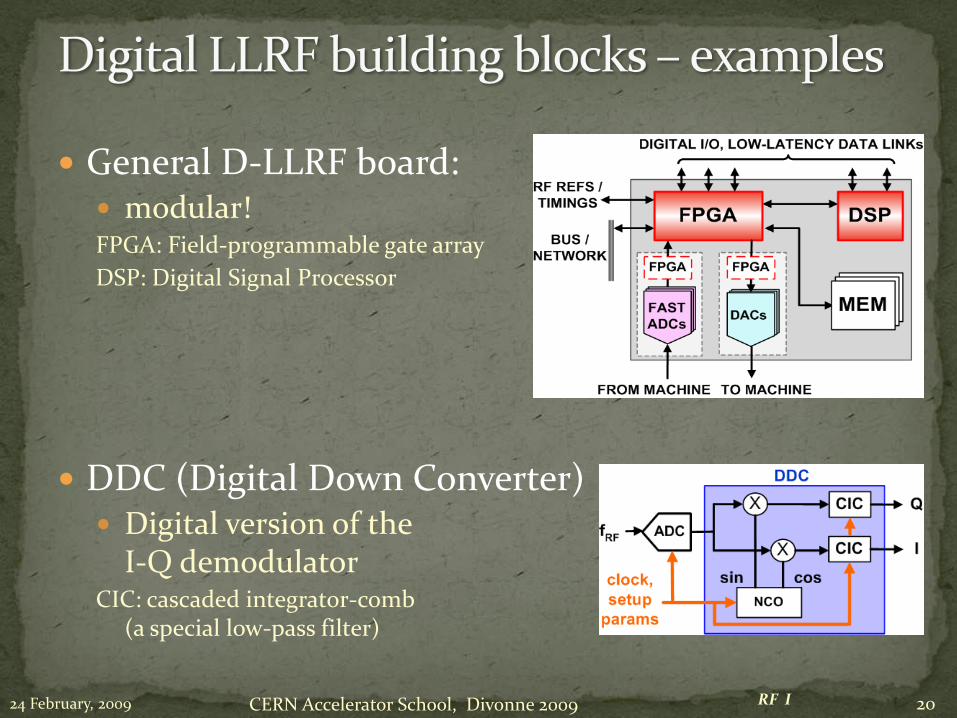
General D-LLRF board: modular!FPGA: Field-programmable gate array
DSP: Digital Signal Processor
DDC (Digital Down Converter) Digital version of the
I-Q demodulatorCIC: cascaded integrator-comb
(a special low-pass filter)
RF I 2024 February, 2009

CERN Accelerator School, Divonne 2009
e.g.: … for a synchrotron:
Cavity control loops
Beam control loops
21RF I24 February, 2009

CERN Accelerator School, Divonne 2009 RF I
• The frequency has to be controlled to follow the magnetic field such that the beam remains in the centre of the vacuum chamber.
• The voltage has to be controlled to allow for capture at injection, a correct bucket area during acceleration, matching before ejection; phase may have to be controlled for transition crossing and for synchronisation before ejection.
Low-level RF High-Power RF
2224 February, 2009

CERN Accelerator School, Divonne 2009 RF I
• Compares actual RF voltage and phase with desired and corrects. • Rapidity limited by total group delay (path lengths) (some 100 ns).• Unstable if loop gain =1 with total phase shift 180 ° – design requires to stay
away from this point (stability margin)• The group delay limits the gain·bandwidth product.• Works also to keep voltage at zero for strong beam loading, i.e. it reduces
the beam impedance.
je
2324 February, 2009

CERN Accelerator School, Divonne 2009
• Without feedback,
where
• Detect the gap voltage, feed it back to IG0 such that
where G is the total loop gain (pick-up, cable, amplifier chain …)
• Result:
• Gap voltage is stabilised! • Impedance seen by the beam is reduced by
the loop gain!
• Plot on the right: vs. ω
with the loop gain varying from 0 to 50 dB
24RF I24 February, 2009

CERN Accelerator School, Divonne 2009
The speed of the “fast RF feedback” is limited by the group delay – this is typically a significant fraction of the revolution period.
How to lower the impedance over many harmonics of the revolution frequency?
RF I
Remember: the beam spectrum is limited to relatively narrow bands around the multiples of the revolution frequency!
Only in these narrow bands the loop gain must be high!
Install a comb filter! … and extend thegroup delay to exactly 1 turn – in this casethe loop will have the desired effect andremain stable!
0.5 1.0 1.5 2.0
2
4
6
8
10
2524 February, 2009

CERN Accelerator School, Divonne 2009 RF I
• Compares the detected cavity voltage to the voltage program. The error signal serves to correct the amplitude
2624 February, 2009

CERN Accelerator School, Divonne 2009 RF I
• Tunes the resonance f of the cavity to minimize the mismatch of the PA.• In the presence of beam loading, this may mean fr ≠f.• In an ion ring accelerator, the tuning range might be > octave!• For fixed f systems, tuners are needed to compensate for slow drifts.• Examples for tuners:
• controlled power supply driving ferrite bias (varying µ),• stepping motor driven plunger,• motorized variable capacitor, …
2724 February, 2009

CERN Accelerator School, Divonne 2009
Horizontal axis: the tuning angle
Vertical axis: the beam current
Hashed: unstable area (Robinson criterion)
Line: (matching condition)
Parameter:
RF I
Phasor diagram for point marked (fixed IB and φz)
2824 February, 2009

CERN Accelerator School, Divonne 2009 RF I
• Longitudinal motion:
• Loop amplifier transfer function designed to damp • synchrotron oscillation. Modified equation:
2924 February, 2009

CERN Accelerator School, Divonne 2009
Radial loop: Detect average radial position of the beam,
Compare to a programmed radial position,
Error signal controls the frequency.
Synchronisation loop: 1st step: Synchronize f to an external frequency (will also
act on radial position!).
2nd step: phase loop
…
RF I 3024 February, 2009

CERN Accelerator School, Divonne 2009 31RF I24 February, 2009

CERN Accelerator School, Divonne 2009 32RF I24 February, 2009

CERN Accelerator School, Divonne 2009
Wave vector : the direction of is the direction of propagation,the length of is the phase shift per unit length.
behaves like a vector.
RF I
z
x
Ey
φ
3324 February, 2009

CERN Accelerator School, Divonne 2009
The components of are related to the wavelength in the direction of
that component as etc. , to the phase velocity as .
z
x
Ey
34RF I24 February, 2009

CERN Accelerator School, Divonne 2009
+=
Metallic walls may be inserted where without perturbing the fields.
Note the standing wave in x-direction!
z
x
Ey
This way one gets a hollow rectangular waveguide
35RF I24 February, 2009

CERN Accelerator School, Divonne 2009
Fundamental (TE10 or H10) modein a standard rectangular waveguide.
E.g. forward wave
electric field
magnetic field
power flow:
z
z
-y
power flowx
x
power flow
36RF I24 February, 2009

CERN Accelerator School, Divonne 2009
e.g.: TE10-wave in rectangular waveguide:
general cylindrical waveguide:
In a hollow waveguide: phase velocity > c, group velocity < c
free space, /c
“slow” wave
“fast” wave
37RF I24 February, 2009

CERN Accelerator School, Divonne 2009
free space, /c
TE10
TE10
TE20
TE01
38RF I24 February, 2009

CERN Accelerator School, Divonne 2009
Also radial waves may be interpreted as superpositions of plane waves.
The superposition of an outward and an inward radial wave can result in the field of a round hollow waveguide.
39RF I24 February, 2009

CERN Accelerator School, Divonne 2009
TE11: fundamental mode TE01: lowest losses!TM01: axial electric field
parameters used in calculation: f = 1.43, 1.09, 1.13 fc , a: radius
40RF I24 February, 2009
CERN Accelerator School, Divonne 2009 41RF I24 February, 2009

CERN Accelerator School, Divonne 2009
Same as above, but twocounter-running waves of identical amplitude.
electric field
magnetic field(90º out of phase)
no net power flow:
42RF I24 February, 2009

CERN Accelerator School, Divonne 2009
electric field magnetic field
(only 1/8 shown)
TM010-mode
43RF I24 February, 2009

CERN Accelerator School, Divonne 2009
The only non-vanishing field components :
h
Ø 2a
44RF I24 February, 2009

CERN Accelerator School, Divonne 2009 45RF I24 February, 2009

CERN Accelerator School, Divonne 2009
gap voltage
• We want a voltage across the gap!
• The limit can be extended with a material
which acts as “open circuit”!
• Materials typically used:
– ferrites (depending on f-range)
– magnetic alloys (MA) like Metglas®, Finemet®,
Vitrovac®…
• resonantly driven with RF (ferrite loaded
cavities) – or with pulses (induction cell)
• It cannot be DC, since we want the beam tube on ground potential.
• Use
• The “shield” imposes a
– upper limit of the voltage pulse duration or – equivalently –
– a lower limit to the usable frequency.
46RF I24 February, 2009

CERN Accelerator School, Divonne 2009
At
BsE
dd
compare: transformer, secondary = beam
Acc. voltage during B
ramp.
47RF I24 February, 2009

CERN Accelerator School, Divonne 2009
PS Booster, „980.6 – 1.8 MHz,< 10 kV gapNiZn ferrites
48RF I24 February, 2009
CERN Accelerator School, Divonne 2009 49RF I24 February, 2009

CERN Accelerator School, Divonne 2009
For slow particles –protons @ few MeV e.g. – the drift tube lengthscan easily be adapted.
electric field
50RF I24 February, 2009

CERN Accelerator School, Divonne 2009 51RF I24 February, 2009

CERN Accelerator School, Divonne 2009
If the gap is small, the voltage is small.zEzd
zE
zeE
z
zc
z
d
dj
If the gap large, the RF field varies notably while the particle passes.
Define the accelerating voltage zeEVz
czgap d
j
Transit time factorExample pillbox:transit time factor vs. h
h/
a
h
a
h
22sin 0101
52RF I24 February, 2009