epmt talk 5june2008
TRANSCRIPT

High average power,
high pulse energy
picosecond lasers
for material processing
Dr. Kurt Weingarten
EPMT conference 5-June-2008, Lausanne, Switzerland

Outline
• Introduction to Time-Bandwidth Products
• Why picosecond lasers might be the “next big thing” in micromachining: faster better (lower cost)
• Overview of the Duetto – flexible picosecond system for micromachining
• Application examples
• Future outlook

Background of Time-Bandwidth Products
• First product sales end of 1996, organically grown (no outside investors)
• Spin-off of ETH Zurich - “SESAM” know-how• Strong technical staff (Ph.D. & masters level)
focused on laser production
• Headquartered at Technopark Zurich
• International network of sale representatives/distributors in all key markets
• Industrial customers in semiconductor, biotech, material processing, etc.
• Products established as reliable in “24-7”operation – for either R&D or industrial applications

-“Simple” piece of semiconductor gives reliable ultrafast laser performance, allowing for a broad range of precision pulsed laser systems
- plus substantial system know-how: laser design, precision opto-mechanics, electronics, etc.
SESAM® – enabling technology
Nonlinear mirror
Time delay (ps)
Ref
lect
ivity
1050
τ long - 10 ps
τ short - 350 fs
SESAM®: semiconductor saturable absorber mirror“Nonlinear mirror” - pulsed light reflects more than continuous light
SESAM®
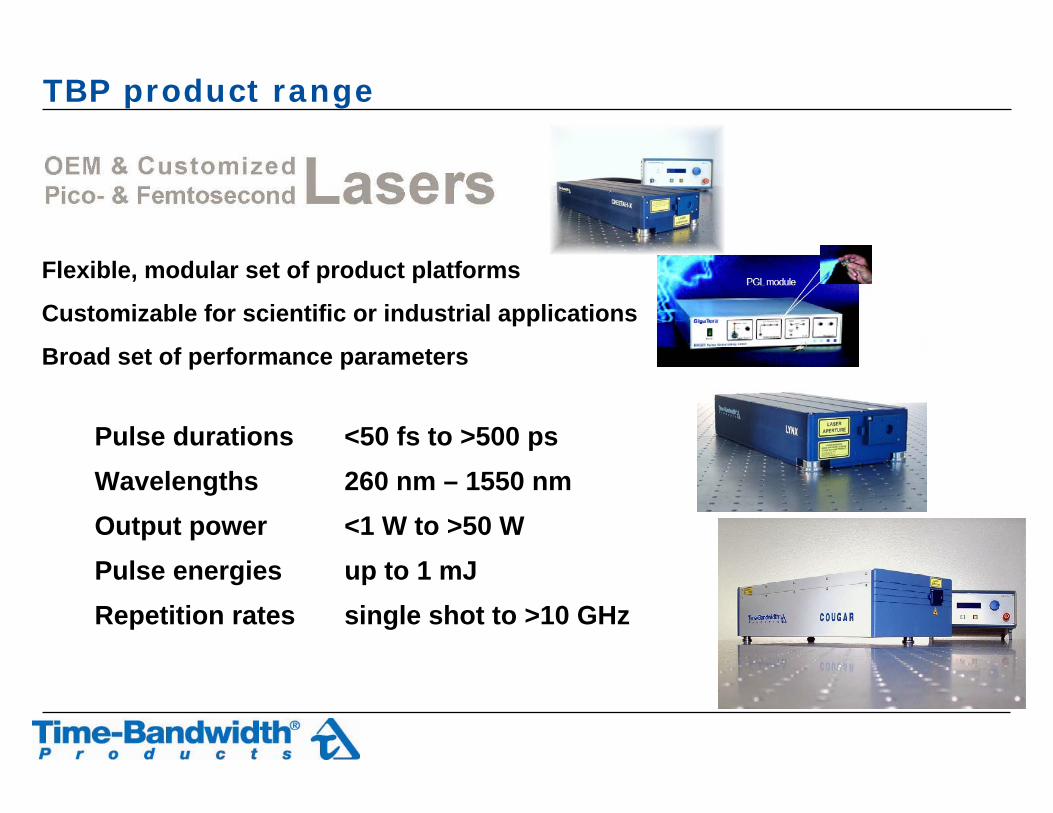
TBP product range
Pulse durations <50 fs to >500 psWavelengths 260 nm – 1550 nmOutput power <1 W to >50 WPulse energies up to 1 mJRepetition rates single shot to >10 GHz
Flexible, modular set of product platforms
Customizable for scientific or industrial applications
Broad set of performance parameters

Material processing: “long” versus “short” pulses
Long pulse:
nanoseconds
Short pulse:
pico- or femtoseconds
Picosecond pulses can cut through “anything” with
a very low amount of heating / residual damage

Material processing: “long” versus “short”
(Mourou et. al. 2002)
“Cold ablation” starts at around 10 ps pulsewidth
Why? Peak Power required to start ablation is reached at lower pulse energy with shorter pulses

• Substantial process advantages compared to nanosecond pulses formicromachining
-smaller heat-affected zone-less micro-cracking-less recast-with substantially faster speed / productivity (depending on process)-higher quality ↔ higher speed ↔ (lower cost)
• Substantial system advantages compared to femtosecond pulses-system much less complex and lower costs-dispersion of picosecond pulses not an issue-system components more proven in industrial environments-power scaling currently possible- “Most of the advantages of femtosecond lasers but much simpler / scalable”
Why picoseconds?

High power / high pulse energy picosecond amplifierWhy consider a picosecond amplifier and not a femtosecond amplifier?
•In the past – many positive research results in material processing with femtosecondTi:sapphire amplifiers.HOWEVER: too complex and too slow (low repetition rate)
TiSA seed laser80 MHz, nJ, 100 fs
Stretcherfs to ns
TiSA amplifierμJ to mJ, Hz to kHz
Q-switched greenPump laser
ns, mJ, Hz to kHz
Compressorns to fs
<150fsμJ to mJHz to kHz
Picosecond amplifier system is much simpler, with increased reliabity and ease of useHigher output powerHigher repetition rateNo stretcher and compressor, no Q-switched green pump laser
DUETTO amplifier
10 ps
10 psμJ to mJHz to MHz
Nd:VAN Nd:VAN

DUETTOTM
Integrated master oscillator power amplifier (MOPA) diode-pumped picosecond laser
Seed oscillator• 1 W average power• 1064 nm wavelength• High repetition rate (quasi-CW)• based on proven LYNX design• Seeds amplifier stage with
user selectablepulse repetition rate
Amplifier stage• > 10 W average power• 1064 nm wavelength• 50 kHz to 8 MHz repetition rate• 10 ps pulsewidth• M2 <1.3 spatial mode quality• based on proven CHEETAH design
Pulse Picker
output power
repetition rate
pulse energy
pulse width
peak power
wavelength
M2 (TEM00)
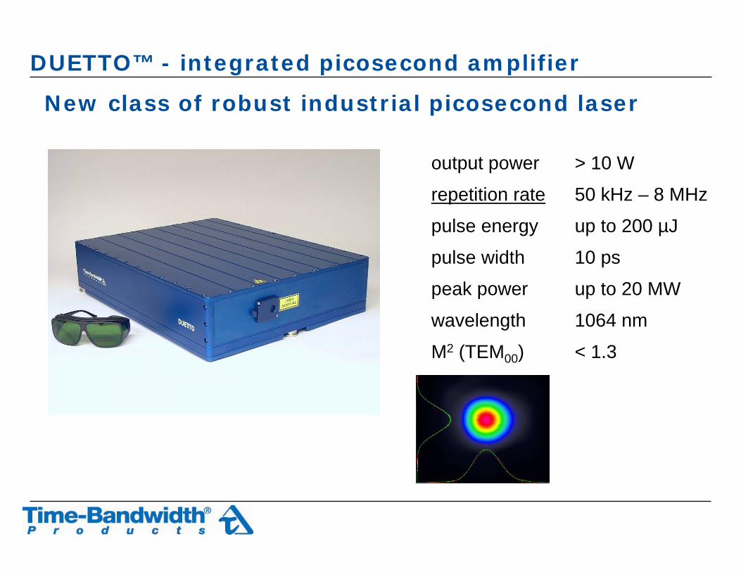
DUETTO™ - integrated picosecond amplifier
New class of robust industrial picosecond laser
> 10 W
50 kHz – 8 MHz
up to 200 µJ
10 ps
up to 20 MW
1064 nm
< 1.3
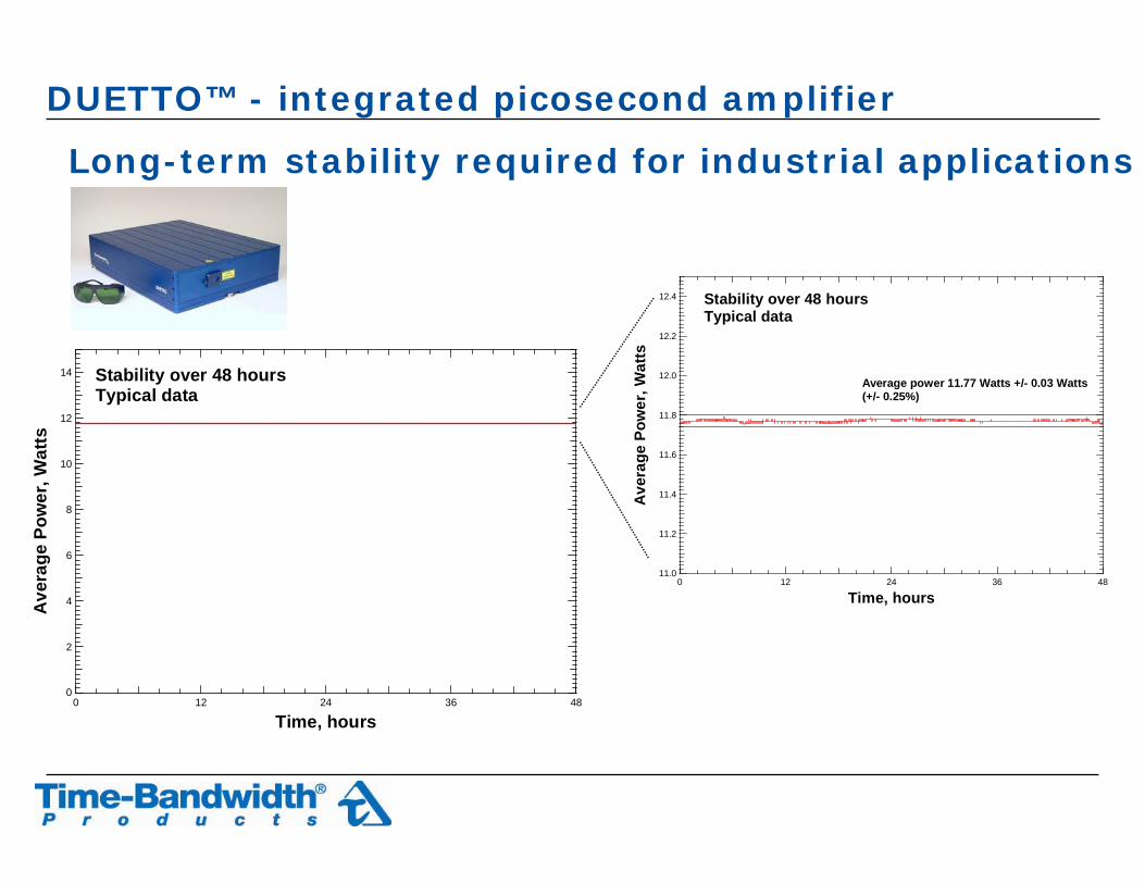
DUETTO™ - integrated picosecond amplifier
Long-term stability required for industrial applications
14
12
10
8
6
4
2
0
Ave
rage
Pow
er, W
atts
483624120
Time, hours
Stability over 48 hoursTypical data
12.4
12.2
12.0
11.8
11.6
11.4
11.2
11.0
Ave
rage
Pow
er, W
atts
483624120
Time, hours
Average power 11.77 Watts +/- 0.03 Watts(+/- 0.25%)
Stability over 48 hoursTypical data

• Power scalable with booster amplifier- FUEGO optional power booster to >50W average power
• Frequency Conversion- to 532 nm (green): >60% conversion efficiency- to 355 nm (UV: >30% conversion efficiency ablative processes- to 266 nm or other wavelengths also available
• Pulse on demand- Optional pulse-on-demand (POD) allows for individually triggerable pulses- or arbitrary groups of pulses- “perfect” pulse selector avoids pre-pulse or first-pulse overshoots typically of other
systems
• Other options- timing synchronization to external clock with sub-picosecond accuracy- variable (switchable) pulsewidths - repetition rate at oscillator output (80 MHz typical)
Duetto: modular customizable approach

• Energy density required for ablation typically 1 Joule / cm2
• 10-100 nm layer removed per pulse: “gentle ablation”
• High repetition rates increase speed limited by scanner speeds and “LFO” = Laser Focus Overlap: “speed limit” due to spot size overlap
• ~10W average power: ~1 mm3 / minute
• up to ~10 mm3 / minute at 50W average power
• Final speed limit depends critically on material, process parameters, and beam delivery limitations
Picosecond Micromachining Guidelines

• Pulse repetition rate of the Duetto scales from 100 kHz to 8 MHz with virtually no change in pulse and beam parameters
-as opposed to Q-switched lasers where pulse quality and stability degrades as repetition rate increases
• Single-pulse processes benefit from higher pulse rate
• “Laser Focus Overlap” (LFO) sets upper speed limit on ablative (line) processes
• Small features require high pulse repetition rate to achieve high scan speed
• Example: spot size 10 µm, LFO 50%-maximum scan speed of 1 m/s at 200 kHz-maximum scan speed of 10 m/s at 2 MHz
Processing speed and pulse repetition rate
75% LFO 50% LFO 25% LFO

• Metals- very thin (thin-film)- precision holes (sub-100 µm)- surface features / tribology
• Semiconductor- hole / via drilling - ablative processes / structures- singulation
• Dielectric- structuring- selective ablation
• “Mixed” materials - picosecond (IR or UV) can cleanly cut / ablate through combinations of the above materials- semiconductor: low-k coated chips- solar: thin-film technologies (CIGS, CdTe, etc)- medical: coated stents
Applications

Application Examples of Duetto: Metals
Columns ablated in copper
Miniature gears in 50 μm stainless steel foil
Sub-100 μm holes (e.g. diesel injectors)
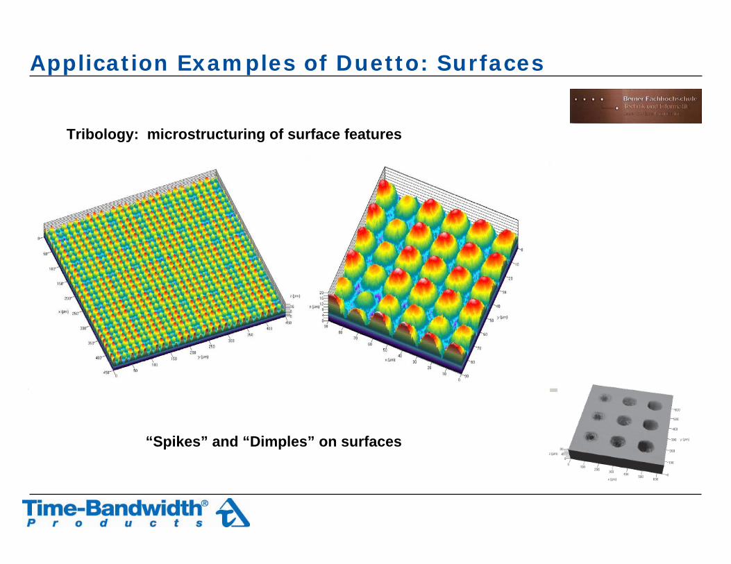
Application Examples of Duetto: Surfaces
Tribology: microstructuring of surface features
“Spikes” and “Dimples” on surfaces
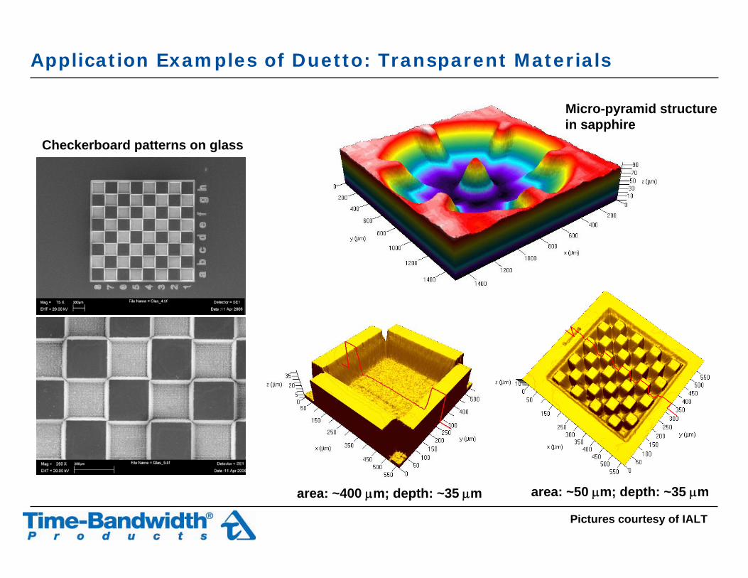
Application Examples of Duetto: Transparent Materials
area: ~400 μm; depth: ~35 μm
Pictures courtesy of IALT
area: ~50 μm; depth: ~35 μm
Checkerboard patterns on glass
Micro-pyramid structure in sapphire

Application Examples of Duetto: Plastics, Polymers
Precise selective ablation of layers on polymer substrate
20 μm plastic foil
Plastic cantilevers 20 μm thickness

Application Examples of Duetto: Others
Deposition of Nanoparticles(Laser Induced Plasma Assisted Ablation LIPAA )
Micro-cutting of paper (no residual burning / damage)

Lightweight and flexible solar cell on polyimide World record efficiency of 14.1%
Voc = 649.4 mV
Jsc = 31.48 mA/cm2
FF = 69.1%
η = 14.1%
Thin film Cu(In,Ga)Se2 solar cell
• Multifunctional layers and heterostructures
• Large area coatings with vacuum and chemical processes
• Laser scribing and patterning of structures
• Monolithically interconnected solar module
ETH Laboratory for Solid State PhysicsLaboratory for Solid State PhysicsThin Film Physics GroupThin Film Physics Group
www.tfp.ethz.ch

Monolithic interconnection in CIGS solar modules
ZnO:Al (1 μm)
CdS or Zns (0.03 μm)CIGS (2 μm)Mo (1 μm)
Substrate
Patterning of front contact & wiring
ZnO:Al Front contact deposition by sputtering
Mo back contact deposition by sputtering
Scribing of Mo by laser beam
CIGS absorber depositionby vacuum evaporation
CdS or ZnS buffer depositionby chemical method
Patterning of buffer/CIGSby laser scribing
ETH Laboratory for Solid State PhysicsLaboratory for Solid State PhysicsThin Film Physics GroupThin Film Physics Group

Application Examples of Duetto: Thin-film solar
• Effective selective ablation - different wavelengths for different material combinations P1 / P2 / P3
• High-quality-no substantial heat affected zone or damage to neighboring material
-no damage of underlying layers
• Fast-Material remove rate is small-LFO sets speed limit-Ultimate challenge is scanner speed and accuracy combined with roll technology

The future: MORE POWER
oscillator domainlow energy
amplifier domainlow speed
100 W10 W
1 W100 mW10 mW
1 kHz 10 kHz 100 kHz 1 MHz 10 MHz 100 MHzRepetition rate
1 mJ
100 µJ
10 µJ
1 µJ
100 nJ
10 nJ
1 nJ
Pul
se e
nerg
y
FORTIS™
FUEGO &DUETTO™
FASTER Processing
Other Wavelengths (Green, UV)

Summary
• Picosecond lasers offer improved quality and faster processing speed for “fine” ablation processes
• Duetto – flexible picosecond system for micromachining
• Flexible and broad repetition rate changing for process optimization
• Wavelength flexibility (IR, green, UV)
• Thin-film applications
• Semiconductor, biotech, solar cell, security
• Future outlook: Higher power higher pulse rates faster processing speed (ultimately limited by scanner / beam delivery technology)

Other applications
• Analysis• Wafer inspection, Multi-photon microscopy, CARS, FLIM
• Medical applications• Ophthalmology, Laser dissection
• Metrology•Optical clocking, Optical sampling, Laser ranging
• Optical communication• Special high-performance data transmission
• Wavelength conversion• Visible / UV wavelengths, optical parametric oscillators, THz generation
• High-Energy Physics• Photocathode illumination, EUV & X-ray generation
Many Thanks
• To Professor Beat Neuenschwander and team at IALT in Burgdorf for all the application support!