epitaxial zintl aluminide sral4 grown on a laalo3 … zintl aluminide sral 4 grown on a laalo 3...
TRANSCRIPT
PHYSICAL REVIEW B 88, 045314 (2013)
Epitaxial Zintl aluminide SrAl4 grown on a LaAlO3 substrate
Lukas Schlipf,1 Alexander Slepko,1 Agham B. Posadas,1 Heidi Seinige,1 Ajit Dhamdhere,2
Maxim Tsoi,1 David J. Smith,2 and Alexander A. Demkov1,*
1Department of Physics, The University of Texas at Austin, Austin, Texas 78712, USA2Department of Physics, Arizona State University, Tempe, Arizona 85287, USA
(Received 11 December 2012; revised manuscript received 11 April 2013; published 17 July 2013)
Zintl phases are a class of intermetallic materials that have simultaneously ionic and covalent bondingresulting from charge transfer between two different atomic species. We present a combined first principlesand experimental study of Zintl-phase SrAl4, which is grown in thin film form on the perovskite oxide LaAlO3
using molecular beam epitaxy. The structural properties are investigated using reflection-high-energy electrondiffraction, x-ray diffraction, and cross-section transmission electron microscopy, which reveal relaxed epitaxialisland growth. Photoelectron spectroscopy measurements verify the Zintl-Klemm nature of the bonding in thematerial and are utilized to determine the band offset and the work function of SrAl4, while transport measurementsconfirm its metallic behavior. The experimentally observed properties are confirmed using density functionalcalculations.
DOI: 10.1103/PhysRevB.88.045314 PACS number(s): 73.20.−r, 73.40.Ns, 73.30.+y
I. INTRODUCTION
Zintl phases, first characterized in the 1930s, are com-pounds usually of the form AaXx = (An+)a[X(an/x)−]x , whereA is an alkali/alkaline earth metal of group 1 or 2 in thePeriodic Table and X is an electronegative metal or semimetalof group 13-15.1 According to the Zintl-Klemm concept, theactive metal A donates valence electrons to the electronegativemetal X, which in turn forms a sublattice with covalentcharacter typical for the isovalent element.2 However, as aresult of the charge transfer, Zintl phases also show ioniccharacter, effectively combining both bonding mechanisms.Because of this dual nature of the chemical bonding in Zintlphases, there has been increased interest in these materials fortheir potential use as thermoelectrics,3 topological insulators,4
and heteroepitaxial buffer layers for dissimilar materials.5
Ideal thermoelectric materials require a combination of goodelectrical conductivity but poor thermal conductivity togetherwith a high Seebeck coefficient. The covalently bonded anionnetwork in a Zintl material provides the electrical conductivity,while the complicated layered structures with large unit cellsdecrease the phonon (thermal) conductivity.3 Zintl phaseswith strong spin-orbit coupling also make good candidatesfor topological insulators. The strong covalency of the orbitalsnear the Fermi level enables strong mixing of states that wouldnormally be at the bottom of the conduction band with statesthat would normally be at the top of the valence band, with thespin-orbit coupling needed to open up a band gap.4
There has been significant interest in the epitaxial inte-gration of functional oxides with semiconductors, especiallysilicon.6 However, one faces several problems when perform-ing heteroepitaxy of crystalline oxides on semiconductors,such as the abrupt change of the nature of the chemicalbonding across the interface, which often disrupts epitaxy.7 Insemiconductors such as Si, the bonding is mainly covalent,but in perovskite oxides, the bonding exhibits a combina-tion of strongly polar covalent and ionic character. Thisbonding transition at the oxide-semiconductor interface canresult in high interfacial energy, which makes wetting lesslikely and often prevents a Frank–van der Merwe (layer-
by-layer) growth mode. Developing a path for the epitaxialgrowth of semiconductors on crystalline oxides could openpossibilities for fabricating novel devices.6 While severaldifferent crystalline oxides can be grown on semiconductors,the growth of semiconductors on oxides usually results inpolycrystalline growth and/or three-dimensional (3D) growthmodes.8 Several successful attempts have been reported, forexample by Bojarczuk et al., using solid phase epitaxy andsurfactants to grow (111)-oriented germanium or silicon on(LaxY1−x)2O3,
9 and the growth of Si(111)/Gd2O3/Si stacksby Osten et al.10,11 An important advance in this field was therealization of so-called crystalline oxide on semiconductors(COS) by McKee et al.12 This group used an interface with thecomposition of Zintl-phase SrSi2 with a thickness of one-halfmonolayer to grow epitaxial SrTiO3 on silicon substrates.13
In this sense, Zintl-Klemm interfaces between oxides andsemiconductors are ideal candidates to enable wetting, thusminimizing interfacial energy. Such an approach has also beendemonstrated for GaAs on SrTiO3.5
In this paper, we consider the Zintl-phase material SrAl4,which can possibly be used for oxide/semiconductor het-eroepitaxy and thermoelectric applications. For this purpose,thin films of SrAl4 are grown on perovskite oxide LaAlO3(LAO) substrates using molecular beam epitaxy (MBE).Aside from crystallographic data, not much is known aboutthe properties of SrAl4. Only very recently has there beensome interest in Mg-Sr-Al alloys containing SrAl4 for use inthe transportation industry.14 Motivated by this, Zhou et al.used first principles density functional theory (DFT) to studythe electronic structure and mechanical properties of SrAl4.15
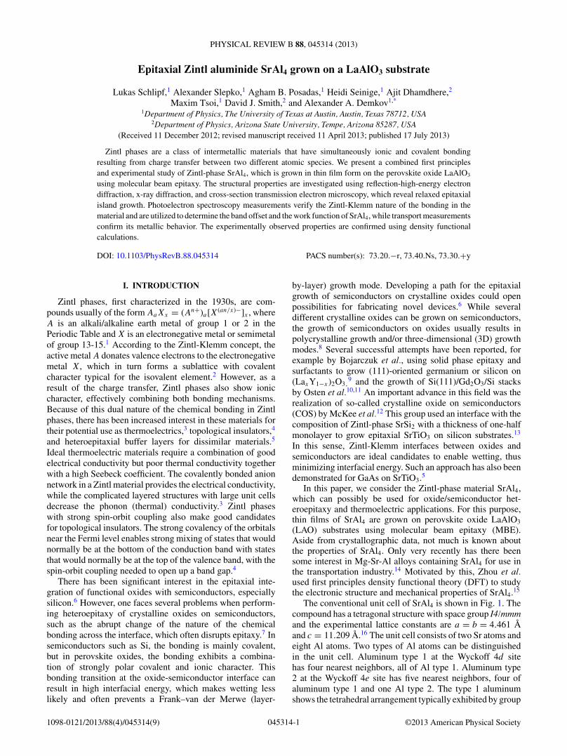
The conventional unit cell of SrAl4 is shown in Fig. 1. Thecompound has a tetragonal structure with space group I4/mmmand the experimental lattice constants are a = b = 4.461 Aand c = 11.209 A.16 The unit cell consists of two Sr atoms andeight Al atoms. Two types of Al atoms can be distinguishedin the unit cell. Aluminum type 1 at the Wyckoff 4d sitehas four nearest neighbors, all of Al type 1. Aluminum type2 at the Wyckoff 4e site has five nearest neighbors, four ofaluminum type 1 and one Al type 2. The type 1 aluminumshows the tetrahedral arrangement typically exhibited by group
045314-11098-0121/2013/88(4)/045314(9) ©2013 American Physical Society
LUKAS SCHLIPF et al. PHYSICAL REVIEW B 88, 045314 (2013)
FIG. 1. (Color online) Conventional unit cell of SrAl4.
14 semiconductors such as silicon, with bond angles close to109.5◦. This is an indication of sp3 hybridization of orbitalsthat is typical for semiconductors with four valence electrons.Hence it can be thought that aluminum, being a group 13element with three valence electrons, received one electronfrom strontium and transformed its bonding characteristics tothat of a group 14 atom. In this simplified view, SrAl4 behavesin accordance with the Zintl-Klemm concept.
In this work, we have synthesized thin films of SrAl4by MBE on LAO and characterized them using reflection-high-energy electron diffraction (RHEED), x-ray diffraction(XRD), atomic-force microscopy (AFM), and transmissionelectron microscopy (TEM). We investigated the electronicstructure and measured the work function using x-ray pho-toelectron spectroscopy (XPS) and ultraviolet photoelectronspectroscopy (UPS) and compared these results to DFTcalculations. We also measured resistivity and Hall effect as afunction of temperature using the van der Pauw geometry.
II. THEORY
We use density functional theory (DFT) to calculate theelectronic structure of the Zintl phase SrAl4. We apply the gen-eralized gradient approximation (GGA) after Perdew, Burke,and Ernzerhof to estimate the exchange-correlation energycontribution to the total energy in the Kohn-Sham equation.17
To solve the Kohn-Sham equation, we use the plane-wave codeVASP along with PAW pseudopotentials as implemented inVASP.18 The valence configuration of Sr is 4s24p65s2, and forAl we use 3s23p1. The energy cutoff in the Fourier expansionof the plane-wave approximation is 500 eV. We found thisenergy cutoff to yield sufficiently good convergence in ourprevious work on SrAl2.19 For the Brillouin zone integration,we use 12 × 12 × 6 and 12 × 12 × 2 Monkhorst-Pack k-point meshes in bulk and surface calculations, respectively.20
In the interface calculation we use a 6 × 6 × 2 k mesh.With these settings, the theoretical lattice constants are4.456 A × 4.456 A × 11.265 A, in excellent agreement withthe experimental values of 4.461 A × 4.461 A × 11.209 A.14
The energy converged to less than 0.01 meV/cell, and the
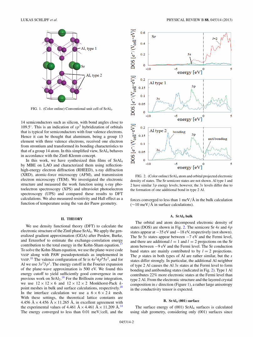
FIG. 2. (Color online) SrAl4 atom and orbital projected electronicdensity of states. The Sr semicore states are not shown. Al type 1 and2 have similar 3p energy levels; however, the 3s levels differ due tothe formation of one additional bond in type 2 Al.
forces converged to less than 1 meV/A in the bulk calculation(∼10 meV/A in surface calculations).
A. SrAl4 bulk
The orbital and atom decomposed electronic density ofstates (DOS) are shown in Fig. 2. The semicore Sr 4s and 4p
states appear at −35 eV and −18 eV, respectively (not shown).The Sr 5s states appear between −7 eV and the Fermi level,and there are additional l = 1 and l = 2 projections on the Sratom between −9 eV and the Fermi level. The Sr conductionband states are mainly contributed to by l = 2 projections.The p states in both types of Al are rather similar, but the s
states differ strongly. In particular, the additional Al neighborof type 2 Al causes the Al 3s states at the Fermi level to formbonding and antibonding states (indicated in Fig. 2). Type 1 Alcontributes 22% more electronic states at the Fermi level thantype 2 Al. From the electronic structure and the layered crystalcomposition in c direction (Figure 1), a rather large anisotropyin the conductivity tensor is expected.
B. SrAl4 (001) surface
The surface energy of (001) SrAl4 surfaces is calculatedusing slab geometry, considering only (001) surfaces since
045314-2
EPITAXIAL ZINTL ALUMINIDE SrAl4 GROWN ON A . . . PHYSICAL REVIEW B 88, 045314 (2013)
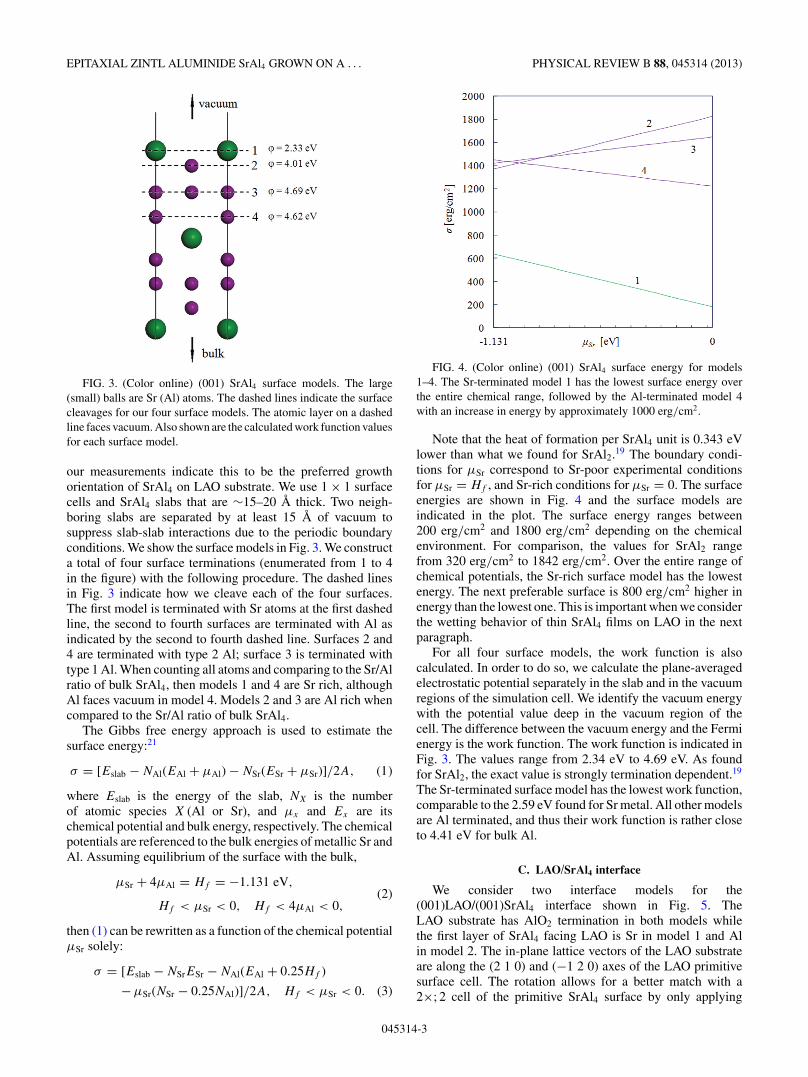
FIG. 3. (Color online) (001) SrAl4 surface models. The large(small) balls are Sr (Al) atoms. The dashed lines indicate the surfacecleavages for our four surface models. The atomic layer on a dashedline faces vacuum. Also shown are the calculated work function valuesfor each surface model.
our measurements indicate this to be the preferred growthorientation of SrAl4 on LAO substrate. We use 1 × 1 surfacecells and SrAl4 slabs that are ∼15–20 A thick. Two neigh-boring slabs are separated by at least 15 A of vacuum tosuppress slab-slab interactions due to the periodic boundaryconditions. We show the surface models in Fig. 3. We constructa total of four surface terminations (enumerated from 1 to 4in the figure) with the following procedure. The dashed linesin Fig. 3 indicate how we cleave each of the four surfaces.The first model is terminated with Sr atoms at the first dashedline, the second to fourth surfaces are terminated with Al asindicated by the second to fourth dashed line. Surfaces 2 and4 are terminated with type 2 Al; surface 3 is terminated withtype 1 Al. When counting all atoms and comparing to the Sr/Alratio of bulk SrAl4, then models 1 and 4 are Sr rich, althoughAl faces vacuum in model 4. Models 2 and 3 are Al rich whencompared to the Sr/Al ratio of bulk SrAl4.
The Gibbs free energy approach is used to estimate thesurface energy:21
σ = [Eslab − NAl(EAl + μAl) − NSr(ESr + μSr)]/2A, (1)
where Eslab is the energy of the slab, NX is the numberof atomic species X (Al or Sr), and μx and Ex are itschemical potential and bulk energy, respectively. The chemicalpotentials are referenced to the bulk energies of metallic Sr andAl. Assuming equilibrium of the surface with the bulk,
μSr + 4μAl = Hf = −1.131 eV,(2)
Hf < μSr < 0, Hf < 4μAl < 0,
then (1) can be rewritten as a function of the chemical potentialμSr solely:
σ = [Eslab − NSrESr − NAl(EAl + 0.25Hf )
−μSr(NSr − 0.25NAl)]/2A, Hf < μSr < 0. (3)
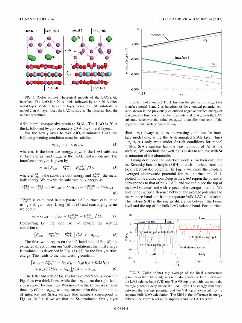
FIG. 4. (Color online) (001) SrAl4 surface energy for models1–4. The Sr-terminated model 1 has the lowest surface energy overthe entire chemical range, followed by the Al-terminated model 4with an increase in energy by approximately 1000 erg/cm2.
Note that the heat of formation per SrAl4 unit is 0.343 eVlower than what we found for SrAl2.19 The boundary condi-tions for μSr correspond to Sr-poor experimental conditionsfor μSr = Hf , and Sr-rich conditions for μSr = 0. The surfaceenergies are shown in Fig. 4 and the surface models areindicated in the plot. The surface energy ranges between200 erg/cm2 and 1800 erg/cm2 depending on the chemicalenvironment. For comparison, the values for SrAl2 rangefrom 320 erg/cm2 to 1842 erg/cm2. Over the entire range ofchemical potentials, the Sr-rich surface model has the lowestenergy. The next preferable surface is 800 erg/cm2 higher inenergy than the lowest one. This is important when we considerthe wetting behavior of thin SrAl4 films on LAO in the nextparagraph.
For all four surface models, the work function is alsocalculated. In order to do so, we calculate the plane-averagedelectrostatic potential separately in the slab and in the vacuumregions of the simulation cell. We identify the vacuum energywith the potential value deep in the vacuum region of thecell. The difference between the vacuum energy and the Fermienergy is the work function. The work function is indicated inFig. 3. The values range from 2.34 eV to 4.69 eV. As foundfor SrAl2, the exact value is strongly termination dependent.19
The Sr-terminated surface model has the lowest work function,comparable to the 2.59 eV found for Sr metal. All other modelsare Al terminated, and thus their work function is rather closeto 4.41 eV for bulk Al.
C. LAO/SrAl4 interface
We consider two interface models for the(001)LAO/(001)SrAl4 interface shown in Fig. 5. TheLAO substrate has AlO2 termination in both models whilethe first layer of SrAl4 facing LAO is Sr in model 1 and Alin model 2. The in-plane lattice vectors of the LAO substrateare along the (2 1 0) and (−1 2 0) axes of the LAO primitivesurface cell. The rotation allows for a better match with a2×; 2 cell of the primitive SrAl4 surface by only applying
045314-3
LUKAS SCHLIPF et al. PHYSICAL REVIEW B 88, 045314 (2013)
FIG. 5. (Color online) Theoretical models of the LAO/SrAl4
interface. The LAO is ∼20 A thick, followed by an ∼20 A thickmetal layer. Model 1 has an Sr layer facing the LAO substrate; inmodel 2 an Al layer faces the LAO substrate. The pictures show therelaxed structures.
4.5% lateral compressive strain to SrAl4. The LAO is 20 Athick, followed by approximately 20 A thick metal layers.
For the SrAl4 layer to wet AlO2-terminated LAO, thefollowing wetting condition must be satisfied:
σSrAl4 + σi < σLAO, (4)
where σi is the interface energy, σLAO is the LAO substratesurface energy, and σSrAl4 is the SrAl4 surface energy. Theinterface energy σi is given by
σi = [Eslab − Ebulk
LAO − EbulkSrAl4
]/2A, (5)
where EbulkLAO is the substrate bulk energy and Ebulk
SrAl4the metal
bulk energy. We rewrite the substrate bulk energy as
EbulkLAO = Ebulk
LAO + 2AσLAO − 2AσLAO = EsurfaceLAO − 2AσLAO.
(6)
EsurfaceLAO is calculated in a separate LAO surface calculation
using slab geometry. Using (6) in (5) and rearranging termswe obtain
σi − σLAO = [Eslab − Esurface
LAO − EbulkSrAl4
]/2A. (7)
Comparing Eq. (7) with (4) we rewrite the wettingcondition as
[Eslab − Esurface
LAO − EbulkSrAl4
]/2A < −σSrAl4 . (8)
The first two energies on the left-hand side of Eq. (8) areextracted directly from our VASP calculations; the third energyis evaluated as described in Eqs. (1)–(3) for the SrAl4 surfaceenergy. This leads to the final wetting condition:
[Eslab − Esurface
LAO − NSrESr − NAl(EAl + 0.25Hf )
+μSr(0.25NAl − NSr)]/
2A < −σSrAl4 . (9)
The left-hand side of Eq. (9) for two interfaces is shown inFig. 6 as two thick lines, while the −σSrAl4 on the right-handside is shown by thin lines. Whenever the thick lines are smallerthan any of the −σSrAl4 wetting can occur for this combinationof interface and SrAl4 surface (the numbers correspond toFig. 4). In Fig. 6 we see that the Sr-terminated SrAl4 layer
FIG. 6. (Color online) Thick lines in the plot are (σi-σLAO) forinterface model 1 and 2 as functions of the chemical potential μSr.Also shown is the previously calculated negative surface energy ofSrAl4-σi as a function of the chemical potential. SrAl4 wets the LAOsubstrate whenever the value (σi-σLAO) is smaller than one of thenegative SrAl4 surface energies −σi .
(line −σ1) always satisfies the wetting condition for inter-face model one, while the Al-terminated SrAl4 layer (lines−σ2,σ3,σ4) only wets under Sr-rich conditions for model4 (this SrAl4 surface has the least amount of Al at thesurface). We conclude that wetting is easier to achieve with Srtermination of the aluminide.
Having developed the interface models, we then calculatethe Schottky barrier height (SBH) at each interface from thelocal electrostatic potential. In Fig. 7 we show the in-planeaveraged electrostatic potential for the interface model 1,plotted in the z direction. Deep in the LAO region the potentialcorresponds to that of bulk LAO, and we can place the top ofthe LAO valence band with respect to the average potential. Weobtain the energy difference between the average potential andthe valence band top from a separate bulk LAO calculation.The p-type SBH is the energy difference between the Fermilevel and the top of the bulk LAO valence band. For interface
FIG. 7. (Color online) x-y average of the local electrostaticpotential in the LAO/SrAl4 supercell along with the Fermi level andthe LAO valence band (VB) top. The VB top is set with respect to theaverage potential deep inside the LAO layer. The energy differencebetween the average potential and the VB top is extracted from aseparate bulk LAO calculation. The SBH is the difference in energybetween the Fermi level in the supercell and the LAO VB top.
045314-4

EPITAXIAL ZINTL ALUMINIDE SrAl4 GROWN ON A . . . PHYSICAL REVIEW B 88, 045314 (2013)
one, the p-type SBH of 2.34 eV is found (the value of 2.63 eVis obtained for interface 2).
III. GROWTH
The growth of SrAl4 on LAO is carried out in a customizedDCA Instruments M600 MBE system with a base pressureof 2 × 10⁻¹⁰ Torr. Al and Sr metal fluxes are introduced tothe substrate surface by heating Knudsen effusion cells to pre-determined temperatures and controlling the growth throughshuttering. The fluxes were calibrated using a quartz crystalmicrobalance incorporated in the MBE system. Additionally,the entire growth process is monitored in situ through adifferentially pumped Staib Instruments RHEED gun attachedto the growth chamber.
For sample growth, polished (100)-oriented LAO singlecrystals with dimensions 5 mm × 5 mm × 0.5 mm manu-factured by CrysTec are used. Below 400 ◦C, LAO has arhombohedral perovskite structure (space group R3c) withlattice constants a = b = c = 3.788 A and angles α = β =γ = 90.022◦.22 LAO undergoes a phase transition to a cubicstructure (space group Pm3m) at 400 ◦C.23 Prior to growth thesubstrates were annealed in vacuum in the MBE chamber for15 min at a temperature of 700 ◦C. The RHEED pattern afterannealing showed a 1 × 1 unreconstructed surface, as shownin Fig. 8(a). Growth of the aluminide film was subsequentlyinitiated at a substrate temperature of 400 ◦C. The sourceswere calibrated to yield a thickness of 1.13 A per min forAl and 3.74 A per min for Sr, which corresponded to equalfluxes for both materials. The deposition was performed underultrahigh-vacuum conditions such that the Al shutter wasconstantly open while the Sr shutter was pulsed, alternatelyopening the shutter for 19 s and closing it for 20 s. Despitethe calibration of the fluxes, this growth process yieldeda 1:4 ratio of Sr:Al on the substrate, indicating a reduced
FIG. 8. (Color online) RHEED patterns of the sample surfaceduring growth recorded along the 〈110〉 direction of LaAlO3 using18-keV electrons: (a) clean LAO surface; (b)–(d) SrAl4 after growthof 1.5 (b), 3 (c), and 7 (d) unit cells of SrAl4. The spots indicatesubstantial step heights on the surface. Two different spacingscorresponding to the 〈110〉 and the 〈100〉 directions of the SrAl4
surface can be observed.
sticking coefficient for Sr at the growth temperature. After thedeposition of about 1.5 unit cells of SrAl4, the RHEED patternfrom the substrate was no longer visible and the crystallinediffraction pattern of SrAl4 could be identified. RHEEDindicated three-dimensional Volmer-Weber growth for SrAl4as the diffraction streaks were interrupted by spots; the patternbecame clearer as the growth was continued [Figs. 8(a)–8(d)].All samples in this study were grown according to this recipeand films were deposited with thicknesses of up to ∼480 Awithout any noticeable change in the RHEED pattern.
After growth, the samples were cooled down to roomtemperature and transferred in situ to the XPS/UPS system viaa vacuum buffer line. Ex situ x-ray diffraction (XRD), atomicforce microscopy (AFM), transmission electron microscopy(TEM), and dc conductivity measurements in the van der Pauwgeometry were then performed as described below.
IV. RESULTS AND DISCUSSION
Typical RHEED patterns of the thin SrAl4 films are shownin Figs. 8(c) and 8(d). Two different spacings can be identifiedwith the 〈100〉 and the 〈110〉 directions of the (001) SrAl4surface. The in-plane lattice constants of the film can becalculated assuming an in-plane lattice constant of aLAO,〈100〉 =3.788 A in Fig. 8(a). The measured in-plane spacings forthe film are aSrAl4,〈110〉 = 3.14 A and aSrAl4,〈100〉 = 4.43 Ain excellent agreement with the lattice constant reportedin the literature aSrAl4,〈100〉 = 4.461 A,16 indicating a nearlyunstrained film. All samples exhibited spotty features inRHEED indicating 3D scattering of the electrons that could beattributed to large surface step heights. The RHEED patternshows two different film orientations in epitaxial registry tothe substrate: 〈110〉SrAl4//〈110〉LAO and 〈100〉SrAl4//〈110〉LAO.Furthermore, no significant change in the RHEED patternswas seen when the growth temperature was varied between400 ◦C and 800 ◦C.
Symmetric 2θ -θ x-ray diffraction measurements werecarried out ex situ to obtain the out-of-plane lattice constant.The scan shown in Fig. 9 reveals an out-of-plane latticespacing of n × 5.59 A and a substrate spacing of n × 3.77 A.Comparing this value to all known stable phases of the Sr-Alsystem,24 there is excellent agreement solely with the (001)orientation of the SrAl4 lattice cSrAl4,〈001〉 = 11.209 A,16 whilethe absence of other peaks confirms the pure (001) orientationof the unstrained epitaxial film.
Figure 10 shows an ex situ AFM image of a sample aftergrowth of about 11 unit cells of SrAl4. Rectangular islands ofdifferent heights are clearly visible over the 2 μm × 2 μmarea. The median island width is on the order of 0.2 μm, alsoseen from the spectral distribution maximum of the Fouriertransform of the surface image (∼10−2.3 nm−1). The islandheights vary in the range 5 to 25 nm, indicating step heightsgreater than several unit cells. The root mean square overheights measured is in the range of 6–8 nm, independentof deposition time. It is interesting to note that neither thesubstrate growth temperature nor the deposition time greatlyaltered the island shape and size. These results confirm thethree-dimensional Volmer-Weber growth mode suggested byRHEED. Furthermore, another structure of the film on theorder of 0.1 mm was visible under an optical microscope
045314-5

LUKAS SCHLIPF et al. PHYSICAL REVIEW B 88, 045314 (2013)
FIG. 9. Typical XRD θ -2θ scan of a 16-nm-thick SrAl4 filmshowing preferred (001) orientation. The unlabeled peaks near theLAO substrate peaks are from the substrate as confirmed from ameasurement of a bare substrate.
(not shown). This structure, however, is related to the topog-raphy of the LAO substrate as a result of twinning.25
The Volmer-Weber growth mode was also confirmed byex situ TEM characterization, with electron micrographsshowing the existence of islands as suggested by AFM andRHEED. Figure 11 shows a cross-sectional TEM image ofsuch an island of thin SrAl4 grown according to the abovedescribed recipe and capped with 4 nm of polycrystalline Ge
FIG. 10. (Color online) AFM image of the surface of 25 nm SrAl4
deposited on LAO (top) alongside plots of the spectral distribution ofthe Fourier transform of the surface image (lower left) and a heightdistribution (lower right).
FIG. 11. Cross-sectional TEM image of 16-nm-thick crystallineSrAl4 on (100) oriented LAO capped with 4 nm of polycrystallinegermanium.
to prevent interaction with air. The SrAl4 island shows epitaxialregistry with the substrate and a high degree of crystallinity.
For x-ray photoelectron spectroscopy of the samples, it isnecessary to work around the problem of charging effects dueto the insulating LAO substrate. For this purpose, the LAO sub-strate was bonded onto heavily p-doped silicon, while at thesame time creating a conducting channel from the Si surface tothe LAO surface by means of Ag paste. Subsequently, in situXPS and UPS were performed on SrAl4/LAO samples usinga VG Scienta MX 650 monochromated Al Kα (1486.7 eV)x-ray source and a VG Scienta VUV 5000 ultraviolet lightsource utilizing the He I (21.22 eV) line, without observingany charging effects. In addition to the energy level of Alatoms in the LAO lattice, the recorded XPS spectra of the Al2p core level in Fig. 12 show another core level at 72.67 eVthat can be attributed to Al 2p3/2 in the SrAl4 lattice. Whenfitting Al core levels with symmetric Gaussian or Lorentzianfunctions, an additional peak needs to be introduced to accountfor the natural asymmetry in metallic Al.26 Although one mightexpect two distinct Al 2p core levels for the SrAl4 lattice dueto the slightly different chemical environments, only one levelfor both types of Al could be resolved. The Sr 3d spectrumin Fig. 12 lies at an energy of 133.44 eV for the 3d5/2 leveland is overlapped with a plasmon feature from aluminum.27
XPS core level binding energies are conventionally referencedto the Fermi level of the spectrometer due to the experimentalsetup.
To determine the true chemical shift of elements withrespect to their bulk values in different materials, the measuredbinding energy values must be referenced to the vacuumlevel by adding the work function of the material. Thus thework function of bulk SrAl4 can be determined in the (001)direction by UPS analysis of the electron energy cutoff usinga sample in which no photoelectrons of the LAO substratewere detectable. The work function of SrAl4 was found to beφ(001) = 3.05 eV. Hence the chemical shifts of the Al 2p3/2
level and the Sr 3d5/2 level in SrAl4 can be obtained withrespect to their measured values in polycrystalline Al metal(72.75 eV) and polycrystalline Sr metal (134.28 eV) and arefound to be �Al = −1.36 eV and �Sr = −0.38 eV, wherea negative value means a shift to lower binding energies.This can be interpreted as confirmation of SrAl4 as a Zintlphase: Sr donates electrons to Al, which assumes, at least
045314-6

EPITAXIAL ZINTL ALUMINIDE SrAl4 GROWN ON A . . . PHYSICAL REVIEW B 88, 045314 (2013)
FIG. 12. (Color online) XPS spectra of Sr 3d core level (left) and Al 2p core level (right) of a 12-nm-thick SrAl4 film grown on LAO.
partly, a structure with four nearest neighbors in a tetrahedralarrangement, with the additional electron lowering the bindingenergy of the Al core levels.
The valence band offset between SrAl4 and LAO was alsomeasured using XPS. The schematic of the measurement isshown in Fig. 13. The positions of the La 3d5/2 level andthe valence band maximum of LAO were measured usinga bulk single crystal of LAO. The valence band maximumwas determined using the linear extrapolation method.28 Theenergy difference between these two levels was found to be832.0 eV. The positions of the Fermi level and the Sr 3d5/2 corelevel of SrAl4 were then determined from a thick (∼16 nm)film of SrAl4 grown on LAO. The Fermi level position wastaken as the midpoint of the measured Fermi edge spectrum.The energy difference between these two levels was found tobe 131.8 eV. Finally, a thin (∼8 nm) film of SrAl4 on LAO wasgrown and the separation between the La 3d5/2 and Sr 3d5/2
levels was determined. The energy difference was measured tobe 702.4 eV. From these three energy differences, the valence
FIG. 13. (Color online) Schematic energy band diagram of energylevels used in the XPS valence band offset determination betweenLAO and SrAl4.
band offset is calculated to be 2.2 ± 0.2 eV with the Fermilevel of SrAl4 above the valence band top of LAO. The mainsource of error comes from the uncertainty in positioning thevalence band top using the linear extrapolation method. Themeasured valence band offset is in excellent agreement withthe theoretical value of 2.34 eV for the model structure withthe Sr layer at the interface.
The island morphology of the SrAl4 may be related to theinstability of the LaO-terminated LAO/SrAl4 interface andthe mixed termination of the LAO surface. Comparison of thework function calculations with the measured value of 3.05 eVsuggests that the surfaces of the SrAl4 films are primarily Srterminated, with possibly some intermixed Al termination.The calculations also suggest that this corresponds to thelowest energy SrAl4 surface. The surface termination of LAO isreported to be temperature dependent, being exclusively AlO2
terminated below approximately 150 ◦C and LaO terminatedabove 250 ◦C after annealing periods exceeding 8 h withtemperatures above 800 ◦C.29 More recent studies suggestboth terminations at room temperature with purely La-Otermination at temperatures above 727 ◦C.30 While our growthis carried out at a temperature well above 250 ◦C, we havenot independently determined the termination of our LAOsubstrates, and since annealing periods in this work arerelatively short and only at 700 ◦C, it is possible that our LAOsurface has mixed termination. From our DFT calculations,we see that wetting is possible for Sr-terminated SrAl4 onAlO2-terminated LAO. The observed island growth possiblyarises from growth on a mixed termination LAO surface, withthe aluminide islands growing preferentially over patches ofAlO2-terminated LAO, as theoretically predicted. The closeagreement between the theoretical Schottky barrier height of2.3 eV and experimental valence band offset of 2.2 eV lendsfurther support to this hypothesis.
The transport properties of SrAl4 films were investigatedover a wide temperature range from 2.3 K to 300 K. Thetemperature dependence of the resistivity and Hall resistivity ofa 70-nm-thick SrAl4 film on LAO were measured in magneticfields up to 8 T applied perpendicular to the film plane.The measurements were done in a standard van der Pauwgeometry with four contact probes located at the corners ofa 5-mm-square sample. The temperature dependence of thein-plane resistivity [Fig. 14(a)] shows the expected behaviorfor metals with a room temperature value of ρSrAl4 (300 K) =45.2 μ cm, dropping linearly until 75 K with a decreasingslope afterwards approximately following a T 2 dependence,which suggests a large contribution from electron-electron
045314-7

LUKAS SCHLIPF et al. PHYSICAL REVIEW B 88, 045314 (2013)
FIG. 14. (a) Resistivity, (b) carrier density, and (c) mobility of a 70-nm-thick SrAl4 slab is measured in the temperature region from2.3 to 300 K.
scattering. However, the resistivity around 10 K shows aglobal minimum in the measured temperature region, whichmay be due to correlation or possibly disorder effects, but isbeyond the scope of this study. The room temperature carrierdensity is nSrAl4 (300 K) = 3.29 × 1022 cm−3 while the roomtemperature mobility is 4.19 cm2/V s, as determined fromthe Hall resistivity. Furthermore, the material also exhibitspositive magnetoresistance (not shown). The carrier densityobtained by integrating the theoretical density of states overthe conduction band amounts to roughly nSrAl4 (300 K) =1.0 × 1023 cm−3, which is about three times larger than themeasured value. This discrepancy might result from the highdegree of film roughness. The real film thickness may varysignificantly over the film area compared to the nominal value,which could reduce the carrier density value calculated fromHall measurements.
V. SUMMARY
We have studied thin films of SrAl4 grown by MBE on(100)-oriented LAO substrates and characterized structuraland electrical properties of the thin aluminide film. RHEED,
XRD, and TEM demonstrated the epitaxial Volmer-Webergrowth mode of an unstrained, (001)-oriented SrAl4 filmwith a mean island size of ∼0.2 μm. Optimal results forcrystalline structure and composition were achieved witha pulsed evaporation technique. XPS analysis confirmedelectron transfer into aluminum in the Zintl-Klemm sense,with a chemical shift to lower binding energies. Comparisonof the experimental work function of φ(001) = 3.05 eV withDFT calculations suggested that the surface was mostly Srterminated. Experimental determination of the band offset like-wise shows excellent agreement with the suggested interfacemodel. Transport properties showed behavior consistent withthe expected semimetallic nature of the material.
ACKNOWLEDGMENTS
This work is supported by the National Science Foundationunder Grant No. DMR1006725, and Texas Advanced Com-puting Center. The authors acknowledge use of the facilitiesin the John M. Cowley Center for High Resolution ElectronMicroscopy at Arizona State University. H.S. and M.T. aresupported in part by NSF Grant No. DMR-1207577.
*[email protected]. Zintl, Z. Phys. Chem. 154, 1 (1931).2T. F. Faessler, Zintl Phases: Principles and Recent Developments(Springer, Berlin, 2011).
3G. J. Snyder and E. S. Toberer, Nat. Mater. 7, 105 (2008).4R. J. Cava, H. Ji, M. K. Fuccillo, Q. D. Gibson, and Y. S. Hor,arXiv:1302.1059 [cond-mat.mtrl-sci].
5A. A. Demkov, H. Seo, X. Zhang, and J. Ramdani, Appl. Phys. Lett.100, 71602 (2012).
6J. W. Reiner, A. M. Kolpak, Y. Segal, K. F. Garrity, S. Ismail-Beigi,C. H. Ahn, and F. J. Walker, Adv. Mater. 22, 2919 (2010).
7X. Zhang, A. A. Demkov, H. Li, X. Hu, Y. Wei, and J. Kulik, Phys.Rev. B 68, 125323 (2003).
8L. Largeau, J. Cheng, P. Regreny, G. Patriarche, A. Benamrouche,Y. Robach, M. Gendry, G. Hollinger, and G. Saint-Girons, Appl.Phys. Lett. 95, 011907 (2009).
9N. A. Bojarczuk, M. Copel, S. Guha, V. Narayanan, E. J. Preisler,F. M. Ross, and H. Shang, Appl. Phys. Lett. 83, 5443 (2003).
045314-8

EPITAXIAL ZINTL ALUMINIDE SrAl4 GROWN ON A . . . PHYSICAL REVIEW B 88, 045314 (2013)
10H. J. Osten, A. Laha, M. Czernohorsky, E. Bugiel, R. Dargis, andA. Fissel, Phys. Status Solidi A 205, 695 (2008).
11R. Dargis, A. Fissel, D. Schwendt, E. Bugiel, J. Krugener, T. Wietler,A. Laha, and H. J. Osten, Vacuum 85, 523 (2010).
12R. A. McKee, F. J. Walker, and M. F. Chisholm, Phys. Rev. Lett.81, 3014 (1998).
13A. A. Demkov and X. Zhang, J. Appl. Phys. 103, 103710(2008).
14M. Aljarraha, M. A. Parveza, J. Lib, E. Essadiqib, and M. Medraja,Sci. Technol. Adv. Mater. 8, 237 (2007).
15D. Zhou, J. Liu, and P. Peng, Trans. Nonferrous Met. Soc. China21, 2677 (2011).
16S. Gobel, M. Somer, W. Carrillo-Cabrera, E. M. Peters, K. Peters,and H. G. von Schnering, Z. Kristallogr. 211, 189 (1996).
17J. P. Perdew, K. Burke, and M. Ernzerhof, Phys. Rev. Lett. 77, 3865(1996).
18G. Kresse and J. Hafner, Phys. Rev. B 47, 558 (1993); G. Kresseand J. Furthmuller, Comput. Mater. Sci. 6, 15 (1996); Phys. Rev.B 54, 11169 (1996); G. Kresse and J. Hafner, J. Phys.: Condens.Matter 6, 8245 (1994); G. Kresse and D. Joubert, Phys. Rev. B 59,1758 (1999).
19A. Slepko and A. A. Demkov, Phys. Rev. B 85, 195462 (2012).
20H. J. Monkhorst and J. D. Pack, Phys. Rev. B 13, 5188 (1976).21G.-X. Qian, R. M. Martin, and D. J. Chadi, Phys. Rev. B 38, 7649
(1988).22G. W. Berkstresser, A. J. Valentino, and C. D. Brandle, J. Cryst.
Growth 109, 467 (1991).23J. Yao, P. B. Merrill, S. S. Perry, D. Marton, and J. W. Rabalais, J.
Chem. Phys. 108, 1645 (1998).24S. Srikanth and K. T. Jacob, Z. Metallkd. 82, 675 (1991).25S. A. Hayward, S. A. T. Redfern, and E. K. H. Salje, J. Phys.:
Condens. Matter 14, 10131 (2002).26S. Doniach and M. Sunjic, J. Phys. C: Solid State Phys. 3, 285
(1970).27J. F. Moulder, W. F. Stickle, P. E. Sobol, and K. D. Bomben,
in Handbook of X-ray Photoelectron Spectroscopy, edited byJ. Chastain and R. C. King, Jr., (Physical Electronics, Inc., EdenPrairie, 1995).
28S. A. Chambers, T. Droubay, T. C. Kaspar, and M. Gutowski, J.Vac. Sci. Technol. B 22, 2205 (2004).
29J. P. Jacobs, M. A. San Miguel, and L. J. Alvarez, J. Mol. Struct.390, 193 (1997).
30H. Kawanowa, H. Ozawa, M. Ohtsuki, Y. Gotoh, and R. Souda,Surf. Sci. 506, 87 (2002).
045314-9