enhancement of minority-carrier lifetime by an advanced high temperature annealing method
TRANSCRIPT

w.elsevier.com/locate/tsf
Thin Solid Films 504 (
Enhancement of minority-carrier lifetime by an advanced high temperature
annealing method
Hui Pan a,*, Liying Tong b, Yuanping Feng a, Jianyi Lin a
a Department of Physics, National University of Singapore, Singapore 117542, Singaporeb Tianjin Electronic Materials Institute, Tianjin 300220, PR China
Available online 24 October 2005
Abstract
An advanced annealing method was proposed to enhance the lifetime of minority carriers by obtaining larger defect-free zone and keeping an
amount of oxygen precipitates. We investigated the influence of annealing process on the defect-free zone and oxygen precipitates. In our
experiments, the thickness of defect-free zone reached up to 100 Am. And an amount of oxygen precipitates, which play a great role on impurity
gathering, were kept at the same time. It was found that the lifetime of minority-carrier was proportional to the thickness of defect-free zone. The
lifetime of minority carriers was enhanced by reducing the grown-in defects in the defect-free zone.
D 2005 Elsevier B.V. All rights reserved.
Keywords: Advanced annealing; Lifetime of minority-carrier; Defect-free zone; Oxygen precipitates
1. Introduction
Oxygen density has been an important parameter for the
performance of ULSI. It has been reported that grown-in void
defects were formed owing to the aggregation of excess
vacancies that contained a lot of oxygen inside, called crystal
originated particles (COPs) [1,2]. It is well known that COPs
degrade gate oxide integrity (GOI). So far, in order to decrease
COPs and improve GOI characteristics, there are many
methods been proposed, such as slow cooling during CZ Si
growth and hydrogen annealing at 1200 -C [3]. All of those
methods cannot satisfy the requirements of nano-devices. At
the same time, SiOx precipitates (oxygen precipitates, OP) are
known to act as effective intrinsic gathering (IG) centers that
attract metallic impurities, such as Fe, Cu, and Au. These
transition metals arrive on the wafer surface after being
sublimated from the heating element of the hot furnace or
carried in by process gas from contaminated gas tank or gas
lines [4]. The metallic impurities alone can form deep-level
electrical traps that can be detrimental to integrated circuit
devices [5]. Several papers had reported that doping nitrogen
could reach the double purposes [6], decreasing COPs and
0040-6090/$ - see front matter D 2005 Elsevier B.V. All rights reserved.
doi:10.1016/j.tsf.2005.09.156
* Corresponding author. Tel.: +65 68747900; fax: +65 67776126.
E-mail address: [email protected] (H. Pan).
keeping an amount of OPs. But the method is complicated and
expensive. In our study, we report an advanced annealing
method for eliminating grown-in defect from the surface-active
region and keeping an amount of OPs that act as IG centers
below the surface-active region.
2. Experimental procedure
The silicon wafers used in this study were <100> oriented
100 mm diameter boron-doped CZ-grown crystal with specific
resistivities 25–30 VIcm and oxygen concentration 1.1–
1.3�1018 atom/cm3. Before introducing the Si wafers into
furnace, they were thoroughly cleansed chemically to remove
any organic and metallic contaminates and native oxides on the
surface. A four-step chemical cleaning procedure consisting of
10 min/80 -C NH3IH2O:H2O2 :H2O (1 :1 :5), 2 min/ 25 -CHF:H2O (1 :1), 10 min/80 -C HCl :H2O2 :H2O (1 :1 :5), and 10
min/80 -C NH3IH2O:H2O2 :H2O (1 :1 :5) was used. Between
each chemical cleaning step, the wafers were rinsed for 5 min
with deionized water at 80 -C to remove any residual chemicals.
After the chemical cleaning procedure, the wafers were dried
and then inspected under oblique light for cleanliness.
Before introducing the wafers into furnace, the furnace was
heated to 800 -C. The annealing processes mainly consist of
1200 -C/3 h denudation, 650–850 -C/10 h nucleation, and
2006) 129 – 131
ww
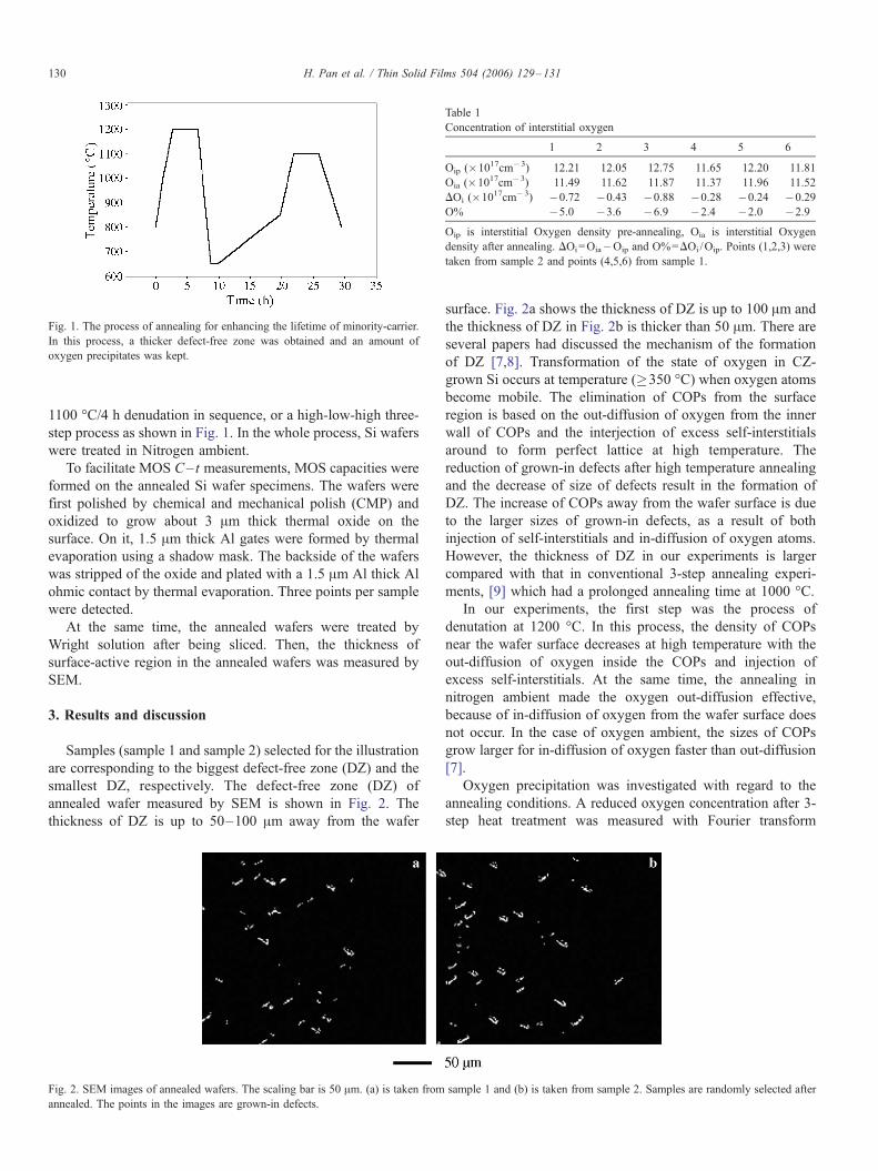
Fig. 1. The process of annealing for enhancing the lifetime of minority-carrier.
In this process, a thicker defect-free zone was obtained and an amount of
oxygen precipitates was kept.
Table 1
Concentration of interstitial oxygen
1 2 3 4 5 6
Oip (�1017cm�3) 12.21 12.05 12.75 11.65 12.20 11.81
Oia (�1017cm�3) 11.49 11.62 11.87 11.37 11.96 11.52
DOi (�1017cm�3) �0.72 �0.43 �0.88 �0.28 �0.24 �0.29O% �5.0 �3.6 �6.9 �2.4 �2.0 �2.9Oip is interstitial Oxygen density pre-annealing, Oia is interstitial Oxygen
density after annealing. DOi=Oia�Oip and O%=DOi /Oip. Points (1,2,3) were
taken from sample 2 and points (4,5,6) from sample 1.
H. Pan et al. / Thin Solid Films 504 (2006) 129–131130
1100 -C/4 h denudation in sequence, or a high-low-high three-
step process as shown in Fig. 1. In the whole process, Si wafers
were treated in Nitrogen ambient.
To facilitate MOS C– t measurements, MOS capacities were
formed on the annealed Si wafer specimens. The wafers were
first polished by chemical and mechanical polish (CMP) and
oxidized to grow about 3 Am thick thermal oxide on the
surface. On it, 1.5 Am thick Al gates were formed by thermal
evaporation using a shadow mask. The backside of the wafers
was stripped of the oxide and plated with a 1.5 Am Al thick Al
ohmic contact by thermal evaporation. Three points per sample
were detected.
At the same time, the annealed wafers were treated by
Wright solution after being sliced. Then, the thickness of
surface-active region in the annealed wafers was measured by
SEM.
3. Results and discussion
Samples (sample 1 and sample 2) selected for the illustration
are corresponding to the biggest defect-free zone (DZ) and the
smallest DZ, respectively. The defect-free zone (DZ) of
annealed wafer measured by SEM is shown in Fig. 2. The
thickness of DZ is up to 50–100 Am away from the wafer
Fig. 2. SEM images of annealed wafers. The scaling bar is 50 Am. (a) is taken from
annealed. The points in the images are grown-in defects.
surface. Fig. 2a shows the thickness of DZ is up to 100 Am and
the thickness of DZ in Fig. 2b is thicker than 50 Am. There are
several papers had discussed the mechanism of the formation
of DZ [7,8]. Transformation of the state of oxygen in CZ-
grown Si occurs at temperature (�350 -C) when oxygen atoms
become mobile. The elimination of COPs from the surface
region is based on the out-diffusion of oxygen from the inner
wall of COPs and the interjection of excess self-interstitials
around to form perfect lattice at high temperature. The
reduction of grown-in defects after high temperature annealing
and the decrease of size of defects result in the formation of
DZ. The increase of COPs away from the wafer surface is due
to the larger sizes of grown-in defects, as a result of both
injection of self-interstitials and in-diffusion of oxygen atoms.
However, the thickness of DZ in our experiments is larger
compared with that in conventional 3-step annealing experi-
ments, [9] which had a prolonged annealing time at 1000 -C.In our experiments, the first step was the process of
denutation at 1200 -C. In this process, the density of COPs
near the wafer surface decreases at high temperature with the
out-diffusion of oxygen inside the COPs and injection of
excess self-interstitials. At the same time, the annealing in
nitrogen ambient made the oxygen out-diffusion effective,
because of in-diffusion of oxygen from the wafer surface does
not occur. In the case of oxygen ambient, the sizes of COPs
grow larger for in-diffusion of oxygen faster than out-diffusion
[7].
Oxygen precipitation was investigated with regard to the
annealing conditions. A reduced oxygen concentration after 3-
step heat treatment was measured with Fourier transform
sample 1 and (b) is taken from sample 2. Samples are randomly selected after
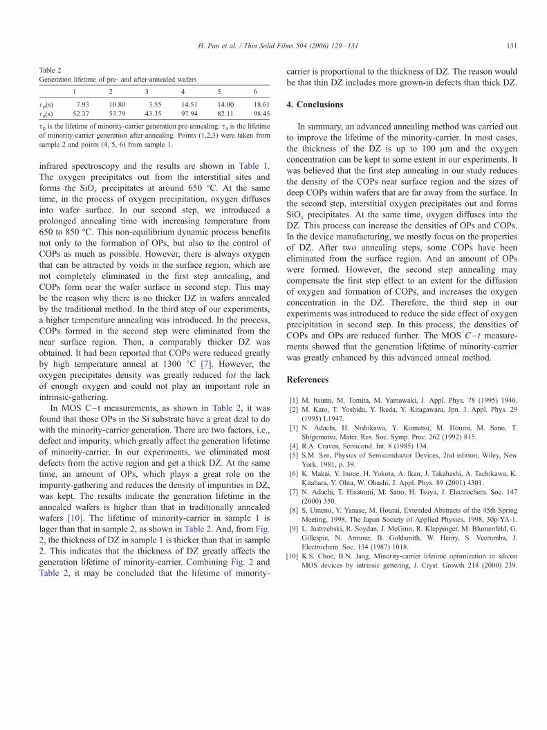
Table 2
Generation lifetime of pre- and after-annealed wafers
1 2 3 4 5 6
sp(s) 7.93 10.80 3.55 14.51 14.00 18.61
sa(s) 52.37 53.79 43.35 97.94 82.11 98.45
sp is the lifetime of minority-carrier generation pre-annealing. sa is the lifetime
of minority-carrier generation after-annealing. Points (1,2,3) were taken from
sample 2 and points (4, 5, 6) from sample 1.
H. Pan et al. / Thin Solid Films 504 (2006) 129–131 131
infrared spectroscopy and the results are shown in Table 1.
The oxygen precipitates out from the interstitial sites and
forms the SiOx precipitates at around 650 -C. At the same
time, in the process of oxygen precipitation, oxygen diffuses
into wafer surface. In our second step, we introduced a
prolonged annealing time with increasing temperature from
650 to 850 -C. This non-equilibrium dynamic process benefits
not only to the formation of OPs, but also to the control of
COPs as much as possible. However, there is always oxygen
that can be attracted by voids in the surface region, which are
not completely eliminated in the first step annealing, and
COPs form near the wafer surface in second step. This may
be the reason why there is no thicker DZ in wafers annealed
by the traditional method. In the third step of our experiments,
a higher temperature annealing was introduced. In the process,
COPs formed in the second step were eliminated from the
near surface region. Then, a comparably thicker DZ was
obtained. It had been reported that COPs were reduced greatly
by high temperature anneal at 1300 -C [7]. However, the
oxygen precipitates density was greatly reduced for the lack
of enough oxygen and could not play an important role in
intrinsic-gathering.
In MOS C–t measurements, as shown in Table 2, it was
found that those OPs in the Si substrate have a great deal to do
with the minority-carrier generation. There are two factors, i.e.,
defect and impurity, which greatly affect the generation lifetime
of minority-carrier. In our experiments, we eliminated most
defects from the active region and get a thick DZ. At the same
time, an amount of OPs, which plays a great role on the
impurity-gathering and reduces the density of impurities in DZ,
was kept. The results indicate the generation lifetime in the
annealed wafers is higher than that in traditionally annealed
wafers [10]. The lifetime of minority-carrier in sample 1 is
lager than that in sample 2, as shown in Table 2. And, from Fig.
2, the thickness of DZ in sample 1 is thicker than that in sample
2. This indicates that the thickness of DZ greatly affects the
generation lifetime of minority-carrier. Combining Fig. 2 and
Table 2, it may be concluded that the lifetime of minority-
carrier is proportional to the thickness of DZ. The reason would
be that thin DZ includes more grown-in defects than thick DZ.
4. Conclusions
In summary, an advanced annealing method was carried out
to improve the lifetime of the minority-carrier. In most cases,
the thickness of the DZ is up to 100 Am and the oxygen
concentration can be kept to some extent in our experiments. It
was believed that the first step annealing in our study reduces
the density of the COPs near surface region and the sizes of
deep COPs within wafers that are far away from the surface. In
the second step, interstitial oxygen precipitates out and forms
SiOx precipitates. At the same time, oxygen diffuses into the
DZ. This process can increase the densities of OPs and COPs.
In the device manufacturing, we mostly focus on the properties
of DZ. After two annealing steps, some COPs have been
eliminated from the surface region. And an amount of OPs
were formed. However, the second step annealing may
compensate the first step effect to an extent for the diffusion
of oxygen and formation of COPs, and increases the oxygen
concentration in the DZ. Therefore, the third step in our
experiments was introduced to reduce the side effect of oxygen
precipitation in second step. In this process, the densities of
COPs and OPs are reduced further. The MOS C – t measure-
ments showed that the generation lifetime of minority-carrier
was greatly enhanced by this advanced anneal method.
References
[1] M. Itsumi, M. Tomita, M. Yamawaki, J. Appl. Phys. 78 (1995) 1940.
[2] M. Kato, T. Yoshida, Y. Ikeda, Y. Kitagawara, Jpn. J. Appl. Phys. 29
(1995) L1947.
[3] N. Adachi, H. Nishikawa, Y. Komatsu, M. Hourai, M. Sano, T.
Shigematsu, Mater. Res. Soc. Symp. Proc. 262 (1992) 815.
[4] R.A. Craven, Semicond. Int. 8 (1985) 134.
[5] S.M. Sze, Physics of Semiconductor Devices, 2nd edition, Wiley, New
York, 1981, p. 39.
[6] K. Makai, Y. Inoue, H. Yokota, A. Ikan, J. Takahashi, A. Tachikawa, K.
Kitahara, Y. Ohta, W. Ohashi, J. Appl. Phys. 89 (2001) 4301.
[7] N. Adachi, T. Hisatomi, M. Sano, H. Tsuya, J. Electrochem. Soc. 147
(2000) 350.
[8] S. Umeno, Y. Yanase, M. Hourai, Extended Abstracts of the 45th Spring
Meeting, 1998, The Japan Society of Applied Physics, 1998, 30p-YA-1.
[9] L. Jastrzebski, R. Soydan, J. McGinn, R. Kleppinger, M. Blumenfeld, G.
Gillespie, N. Armour, B. Goldsmith, W. Henry, S. Vecrumba, J.
Electrochem. Soc. 134 (1987) 1018.
[10] K.S. Choe, B.N. Jang, Minority-carrier lifetime optimization in silicon
MOS devices by intrinsic gettering, J. Cryst. Growth 218 (2000) 239.