engr.case.eduengr.case.edu/merat_francis/eecs245/graymark/graymark_manual.pdfue of a voltage is the...
TRANSCRIPT


PARTS IDENTIFICATION AND INVENTORY EXPERIENCEThis experience is provided to acquaint you with the vari-ous electronic components and fittings included in this
To assist you in proper identification of the major parts and
project. Unpack the project carefully and check (V) eachfittings, pictorial and schematic illustrations are given in
part and fitting against the PARTS LIST In case of incor-Figure 1,
rect, missing, or damaged parts, please refer to How to Or-der Replacement Parts and Graymark’s Warranty.
Upon completion of the parts identification and inventory,have your instructor initial your Progress Guide.
-;DIODE, S IGNAL i
i
uIA@09INTEGRATED CIRCUIT
FUSE HOLDER DIODE, POWER 1, TRANSFORMER
POWER RESISTOR
HEAT SINKLM317-LM337POST, RED, BlACK POTENTIOMETER
R U B B E R F O O T+-_-_-.- S O L D E R L U G.- . . _.- ._ . _d _._~_~__--I
MACHINE SCREWSELF-TAPPING SCREWSf3 x Qmtn AND 2.6 x 5mm
i
SPACER 1OmmAND 4Omm~-_---..-
ELECTROLYTICCAPACITOR PCB
---j----
LM317-LM337
BREADBOARD- - __. -..---_,
LOCK WASHER SPLITSTRAIN RELIEF AND INTERNAL STAR
TRANSISTOR
FIG. 1
5


FIG. 29A
_FlG. 29B
lI
TPl8
0 T:-I 5”
TP17I IOT:+W
1 .I ., RlO 0Dll T&
’ f
r - - - - - - - - - -
i l
, .
I I
I 1 R6
l-/N OJOJI
fTP9l T m .b.
. . . . TPlA
Y E L L O W fl FYELLOWFIG. 30 BUCK+ MBL”E
connect the meter test leads from the powerPlug .
- 24. Position the two portions of the AC power cordgrommet around the cord where it extends out ofrear of the cabinet top, as shown in Fig. 29A. Us-ing slip-joint pliers, insert the grommet into thehole in the rear of the cabinet top as shown in Fig.29BYou will have to squeeze the grommet quitehard with the pliers so that the power cord isformed into a “U” inside the grommet, and thegrommet is compressed enough to fit into thehole.
- 25. Locate the Printed Circuit Board (PCB) and thetest points. Insert and solder TPl through TPl9into the PCB. The test points are inserted fromthe component side of the PCB and soldered tothe copper on the solder side of the PCB. Referto Fig. 30 and the the silkscreened legend on thecomponent side of the PCB for the test pointlocations.
- 26. From the solder side (bottom) of the PCB threadthe transformer leads through the holes in thePCB as shown in Fig. 3O.Then, from the compo-nent side (top) of the PCB, thread the strippedand tinned wire ends through the holes markedYL, BL and BK. Solder these five wires to thePCB, and cut off any excess lead length. Note:This is done so when the board is handled duringcomponent installation and testing, the wireswon’t bend and break at the weak points wherethe wire insulation stops and the tinned copperwire goes through the PCB.
AC VOLTAGE WAVEFORMS AND VALUES
DISCUSSION
Measuring a DC voltage is simple and straight forward.Shown on a graph, the voltage of an automobile batterywould appear as a straight horizontal line. In Fig. 31 the ver-tical axis shows the magnitude of the voltage being meas-ured, and the horizontal axis represents time. The timeshown on the graph would be in the order of several sec.ends, the time it takes for the meter pointer to stabilize andfor you to accurately read the meter.The graph shows thatthe meter test probes were connected to the the battery at
19

time (T) 0, and removed immediately after the meter wasread.
To show an AC voltage, we need to change our graph intwo ways. It will have to indicate voltages of both polarities,positive and negative, and we will have to make the hori-zontal axis cover a much smaller period of time.The publicutility companies in the United States provide 60 Hertzpower. Hertz, abbreviated Hz, means cycles per second.60 Hz means that the polarity of the voltage is reversing120 times a second.
Figure 32 is a graph of the voltage at a wall outlet.The horimzontal axis only covers I/60 of a second of time, or 16.67milliseconds (mS).To observe what this graph shows, youwill have to use an oscilloscope.The AC voltage ranges ofa VOM will indicate the rms voltage, but the meter cannotrespond to the rapid changes of the 60 Hz. AC voltage, andeven if it could your eye could not readmeter pointer.
AC VOLTAGE OBSERVATION andEXPERIENCE
Purpose: To observe and measurePEAK, and RMS Voltages.
Equipment: OSCILLOSCOPEVOM or DMM
the rapidly moving
MEASUREMENT
PEAK, PEAKTO-
- I.
2 .
3 .
- 4.
5.
6 .
- 7.
8 .
9 *
IO.
_ 11.
_ 12.
13.
_ 14.
15
Refer to Fig. 33. Mount the 1 Omm spacers on thesolder side of the PCB using the four 20 x 3mmmachine screws, the two 40mm spacers, andtwo 3mm nuts.
Place the cabinet top assembly, the power trans-former and the PCB on a work surface as shownin Fig. 34.
Set the oscilloscope power switch to On.
Adjust the Oscilloscope to 10 Volts/div. Set thesweep rate to 5mSdiv. Adjust the input controlsto display an AC signal, and vertical positioningat the CENTER line.
Connect the scope ground lead to TP2 of thePCB, and the probe to TPI.
Connect the power plug of the 808 to a 115 VACpower outlet.
Set the power switch to ON.
Record your peak-to-peak reading l
If your reading is about 60 Volts peak to peak,then proceed to the next step. If your reading isnot about 60 Volts peakto-peak, stop, and checkyour test set up or consult your instructor.
Remove the scope probe.
Adjust the VOM or DMM to read 19 Volts AC.
Connect one meter test lead toTP2 of the PCB,and the other test lead to TPI .
Record your reading .
If your reading is about 21 Volts AC, proceed tothe next step. If your reading is not about 21 VoltsAC, then stop and check your test set up or con-sult your instructor.
Remove the test leads.
13.0 wVOLTS- - - -k,
12*-1’
I II I
lO=m I I
!zI I
5 &-I I
i3I II I
: &I I
LIJ I I
!i4i I1 II I
2 .’ I II I
IIV b
TIME
TIME TAKEN-TO READ METER ’
TIME FORMETER TOSTABILIZE
FIG. 31
FIG. 32
FIG. 3320

MATHEMATICAL CALCUUTIONS AND DEFINITIONS
Purpose: To demonstrate that the previous experience isin agreement with the mathematical formulas
The following formulas are used to calculate ROOT MEANSQUARE, PEAK and PEAK-to-PEAK AC sine wave Volt-ages, Refer to Fig. 32.
VP = 1.414 x vrmsVp=.5 x vp_p
VP-P = 2.828 x VrmsVP-P = 2xvp
V fms = .707 x vp
Vfms = .3536 x Vp_p
PEAK VALUE (p): The amplitude of a voltage measuredfrom zero or reference axis to its maximum value, when thevoltage alternates between positive and negative halfcycles.
PEAK-to-PEAK (p-p): The amplitude of a voltage meas-ured from maximum positive peak to maximum negativepeak, when the voltage alternates between positive andnegative half cycles.
ROOT MEAN SQUARE (RMS): The effective or RMS val-ue of a voltage is the SQUARE ROOT of the average(MEAN) of the squares of all the instantaneous values ofthe voltage over one cycle. For a sine voltage, the RMS vai-ue is equal to 0.707 times the maximum peak value of thevoltage.
INSTANTANEOUS VALUE: The exact value of the ampli-tude of a voltage at a particular instant in time.
Using the above formulas, calculate the unknown voltagesin Fig. 35.
This completes the AC VOLTAGE OBSERVATION andMEASUREMENT EXPERIENCE. Have your instructorinitial your progress guide.
MEASUREDVALUE RMS PEAK-TO-PEAK PEAK
54Vp-p115vlms163vp
, 326vp-p .FIG. 35
7 1

DISCUSSION
Figure 36 is a partial block diagram and schematic of the808 Power Supply, showing the rectifiers and associatedcircuitv.
There are three basic types of rectifier circuits: the half-wave, the full-wave center-tapped, and the full-wavebridge. Each of these rectifier circuits uses a different num-ber of diodes and requires a transformer winding with a dif-ferent rating. Figures 36A and 37 identify some of the differ-ences between these three types of circuits.
The first column in Fig. 37 contains the three types of recti-fier circuits. The number of diodes used by each circuit islisted in the second column. The average diode current isshown in the third column.This value has significance be-cause diodes with a higher current rating are required forhalf-wave circuits, as compared to those required by theother two circuits.TheTransformer Power Rating column isalso important, since each type of circuit requires a trans-former or a transformer winding with a different power ca-pacity. And, the larger the power capacity required, thegreater the size and the cost of the transformer.
The Ripple column refers to the percentage of ac voltagecontained in the DC output of the rectifier circuit. A de-crease in the percentage of ripple offers a correspondingdecrease in the amount of capacitance required in the Fil-tering Stage. Since lower value capacitors are smaller insize and cost less, a low percentage of ripple from the recti-fier circuit is desirable.
Finally, the Conversion Efficiency column indicates the eff i-ciency of each Rectifier Circuit in converting alternatingcurrent to direct current. Notice that the full-wave rectifiercircuits are twice as efficient as the half wave circuit.
The heart of the rectifier circuit is the diode. Most diodesare made from silicon or germanium, both of which aresemiconductors. Silicon is used for almost all diodes usedin power supply rectifier circuits, as it is capable of operat-ing a higher temperature than germanium. For a given sizeof device, a silicon diode can pass more current than a ger-manium diode. A diode is a component which will allow cur-rent to flow in one direction - from cathode to anode. Referto Fig. 38.
Alternating current flows first in one direction, then the op-posite direction, then reverses direction again. This alter-nating action occurs continuously. Direct current, on theother hand, flows in only one direction. A diode can be putin the path of an alternating current to block the current flowin one direction and permit the current flow in the oppositedirection. It is in this manner that alternating current is recti-fied or converted into pulsating direct current.
The Graymark Model 808 Power Supply uses four silicondiodes in a full-wave bridge rectifier circuit, and four moresilicon diodes in a center-tapped full-wave bridgerectifier circuit.
The center-tapped full-wave rectifier circuit combines fea-tures of the center-tapped full-wave and the full-wavebridge rectifier circuits. It is used in the 808 Power Supplyto provide power for the 0 to + 15 Volt and the 0 to - 15Volt outputs. Before going on to the FILTERING section,you will build and test four types of rectifier circuits.
-
POWERTRANSFORMER ’
1 4
SEC1
PRI .
RECTIFIER
A
BLUE
TP4?
Tl ATP5
FIG. 36
HALFWAVE RECTIFIERS
DISCUSSION
Half-wave rectifier circuits are sometimes used where thecurrent requirements are low, in the order of 10 to 100microamps, and voltages of 1 kV (1000 Volts) or higher areneeded. Photomultiplier tubes and Ion chambers, whichare used to detect and measure radiation, are examples ofdevices requiring this type of DC power. Utility power sup-plies, such as your Graymark 808, which are generallyused to power solid state analog and digital devices, donot usually use half-wave rectifier circuits.
In the HALFWAVE RECTIFIER TEST, you will be viewingthe output of a half-wave rectifier on an oscilloscope. A1.5K Ohm resistor (Rl 1) is connected across the output of
22
l-lALFwAVE
CENTERTAPPED FULLWAVE
Without it, dangerously high voltages could remain presentFULL WAVE BRIDGE long after the input power has been turned off or
TYPES OF RECTIFIER CIRCUITS disconnected.FIG. 36A
SIGNIFICANT RECTIFIER CIRCUIT CHARACTERISTICSNUMBER AVERME TRANBFDRMER coNvERsloN
ofDlooEB~ P O W E R RiPPLE EFFICIENCYREQUIRED CuRRENr Rmm ,
1 2 1 121 4Q.6
FIG. 37
DIODE
, 1
,
ANODE CATtiODE
ANODE CATHODE
- CURRENT FLOW
FIG. 36the rectifier circuitry. Figure 43 is a schematic of this circuit.Without this resistor, stray circuit capacitances could distortthe waveform displayed on the scope. In the completedPower Supply Rl 1 serves as a bleeder resistor.
One of the functions of a bleeder resistor is to dischargeor “bleed off” the electrical energy remaining in the filter ca-pacitors atier the power supply is turned off. In high voltagesupplies, the bleeder resistor is an important safety device.
FIG. 39
The output voltages of the Model 808 Triple Power Supplyare not high enough to be hazardous to the person usingit, but it is disconcerting when a power supply that has beenturned off earlier generates a spark if an output is acciden-tally shorted. In the 808 Power Supply, bleeder resistors,along with the voltage regulators, serve to discharge the fil-ter capacitors within seconds after the input power hasbeen switched off or disconnected.
When you are building your 808, you will be instructed toinstall some components long before they are used in anexperience.This is to provide a discharge path for the filtercapacitors before the voltage regulators are installed.
In unregulated power supplies the bleeder resistor is isoften designed to draw 10 % or more of the rated outputcurrent.This is to improve the voltage regulation of the sup-ply under changing load conditions.
CONSTRUCTIONRefer to Fig. 39 for the following steps.
1 .
2 .
3 .
Be sure the 808 power plug is NOTconnected toa power outlet.
Mount diode Dl on the PCB. Be sure that thebanded end of the diode is oriented the same asthe diode outline that is silkscreened on the PCB.Using a heat sink as shown in Fig. 40, solder thediode leads to the PCB. cut off any excess leadlength.
Mount resistor Rll, 1 SK Ohm (brown-green-red) .5 Watt, on the PCB. Solder the leads to thePCB and cut off any excess length.
23

Purpose: To observe the current blocking capability of adiode.
Equipment: VOM or DMM
- 1.
2 .
3 .
- 4.
Be sure the 808 power plug is NOTconnected toa power outlet.
Set the meter you are using to its lowest ohmme-ter range. If your meter has an range marked witha diode symbol or the word “diode”, use thatrange instead. Connect the positive* meter testlead to TP8 and the negative* meter test lead toTPl , (If your uncertain what the asterisks afterthe words “positive” and “negative” mean, reviewthe last paragraph of the section titled USING ANOHMMETER ON POLARIZED CIRCUITS ANDCIRCUITRY) Record the resistance reading.
-
Reverse the meter test leads and record the re-sistance reading. Disconnect themeter test leads from the test points.
In the 2nd step, you should have had an infiniteresistance reading, indicating that the direct cur-rent from the ohmmeter was being blocked. Inthe 3rd step, there should have been a much low-er resistance reading, indicating that the currentwas passing through the diode. This illustratesthe ability of a diode to permit current to flow inone direction, and to restrict its flow in the oppo-site direction. The difference between the twoconditions depends upon the polarity of the volt-age applied to the diode. The anode of a diodehas to be at a more positive potential than thecathode for current to flow to occur.
HALFWAVE RECTIFIER EXPERIENCE
Purpose: To observe the voltage waveform produced by aHalf-Wave Rectifier circuit.
Equipment: Oscilloscope
Refer to Fig. 39 for the following steps.
1.
2 .
3 l
4.
5 l
6 .
Be sure the 808 power plug is NOTconnected toa power outlet.
Cut a 125mm length of red 22 gauge wire, andstrip 6mm of insulation from each end.
Solder one end of the red wire to TP8, and theother end toTP17. Because these are temporaryconnections for testing purposes, its not neces-sary to make mechanical connections.
Turn the oscilloscope ON and let it warm up. Ad-just it to display a 60 Volt (peak to peak) 60 Hertz(6OHz) signal. Set the vertical (Y) input couplingto DC.
Connect the oscilloscope (scope) ground lead toTP2, and the scope input probe to TPl.
Plug the 808 Power Supply plug into a power out-let.Turn the power switch ON. Obsewe the wave-form displayed on the scope. It should look likeFig. 41 .This is ac voltage which is present at thesecondary winding of the transformer.
TRANSFORMERSECONDARY
AC VOLTAGEFIG. 41
a CATHODE OF DlHALFWAVE RECTIFICATION
FIG. 42
+
l
--
NOCURRENT
FLOW
+
HALF WAVE RECTIFIER CIRCUITL
FIG. 43
7. Move the scope probe to TP17. The waveformshould look like Fig. 42.This waveform is the re-sult of diode Dl rectifying the ac voltage. Dl clipsoff the negative half of the waveform, leavingonly the positive half. This is called half- waverectification. Current flow in a half-wave rectifiercircuit is illustrated in Fig. 43.
8. Turn the 808 Power switch Off and disconnectthe power plug from the outlet. Disconnect thescope common lead and input Probe. Leave thered wire that is soldered to TP8 and TPl7 inplace.
9. This completes the HalfWave Rectifier Experi-ence. Have your instructor initial your ProgressGuide.
24

FULLWAVE CENTER-TAPPED RECTIFIERS
DISCUSSION
A FuMVave center-tapped rectifier circuit requires a trans-former with a secondary winding which has a tap halfwaybetween both ends of the winding (a center-tap). secondarynumber 2 of the 808 Power Supply transformer is a center-tapped winding. You have already used one half of thiswinding in the HalfWave Rectifier section.
FULLWAVE CENTER-TAPPEDRECTIFIER EXPERIENCE
Pupose: To observe the voltage waveform produced by aFukWave Center-Typed Rectifier circuit.
Equipment: Oscilloscope
Refer to Fig. 44 for the following steps.
1 .
2 .
Be sure that the 808 power plug is NOTconnect-ed to a power outlet.
3 .
4 l
5 .
Solder the cathode lead of a lN5393 diode toTP8 of the PCB, and the anode lead toTP3. Donot cut the diode leads, or remove the red wiresoldered to TP8. This is a temporary installationof D2. This diode will be removed after the full-wave filter test and installed later in its permanentlocation. Since the long leads isolate the heat ofsoldering from the diode itself, it is not necessaryto use a heat sink.
Turn the scope ON and let it warm up. Adjust itto display a 60 Volt (peak to peak) 60 Hz signal.Set the vertical input (Y) coupling to DC.
Connect the scope ground lead toTP2, and the ’I
FIG. 45input probe to TPl7.
Connect the 808 Power Supply plug to a poweroutlet. Turn the power switch ON. The waveformdisplayed on the scope should look like Fig. 45.Both halves of the ac cycle are now being recti-fied. Refer to Fig. 46. Diode’Dl rectifies the cur-rent from one half of the secondary winding, anddiode D2 rectifies the current from the other halfof the winding. Since the diode cathodes areconnected together, both their waveforms arejoined together to produce a composite wave-form. This composite waveform is composed oftwo sets of positive voltage half cycles. One setis from Dl ,and the other set, which is 180 de-grees out of phase with the first set, is from D2.This is called full-wave rectification.
6 . Turn the 808 Power switch OFF and disconnectthe power plug from the outlet. Disconnect thescope common lead and input probe. Leave di-ode D2 and the red wire in place.
7 . This completes the Full-Wave Center-Tapped
0 ;----------- ; cs
IDI? f772
I i 0 0I I - -l I ?!!II Cl1 TPl5I r ---------
FIG. 44*
FULLWAVE RECTIFICATION, POSITIVE OUTPUT
NO CURRENT FLOW
+
CURRENT FLOW
NO CURRENT FLOW
FULLWAVE CENTER-TAPPED RECTIFIER CIRCUITRectifier Test. Have your instructor initial yourProgress Guide.
LFIG. 46

FuMVave bridge rectifiers are used in a wide range of pow-er suppiies.These rectifier circuits are among the most effi-cient and cost effective for many applications.
Refer to Fig. 47 for the following steps.
1 .
2 ,
Be sure the 808 power plug is Not connected toa power outlet.
Mount diodes D5, D6, D7 and D8 on the PCB Besure the banded ends of the diodes are orientedthe same as the diode outlines that are silkscreened on the PCB. Using a heat sink, soldereach diode lead to the PCB, and cut off anyexcess lead length.
FULLWAVE BRIDGE RECTIFIER EXPERIENCE
P~pose: To obsewe the voltage waveform produced by aFullWave Bridge Rectifier circuit.
Equipment: Oscilloscope
1. Be sure the 808 power plug is Not connected toa power outlet.
Refer to Fig. 47 for steps 3 through 6.
2 .
3 .
- 4 .
5 .
6 .
7 .
Solder a 1.5 kOhm (brown-green-red) 5 Watt re-sistor toTP7 and TP9. Cut the leads off close tothe test points. This resistor is for testing pur-poses and will be left in place until the 5 Volt reg-ulator is installedm
Adjust the scope to display a 30 Volt (peak topeak) 60 Hz signal. Set the vertical (Y) inputcoupling to DC.
Connect the scope ground lead to TP7 and theinput probe to TP’ 9-
Plug the 808 Power Supply plug into an outlet.Turn the Power Switch ON. Observe the wave-form displayed on the scope. It should look likeFig. 45. Both the FulLWave Center-Typed andthe FullMIave Bridge produce the same wave-form. Figure 48 illustrates current flow in a Full-Wave Bridge Rectifier circuit.
Turn the 808 Power switch Off and disconnectthe power plug from the outlet. Disconnect thescope ground lead and input probe from the testpoints.
This completes the FullM/ave Bridge RectifierTest. Have your instructor initial your progressguide.
FIG. 47
FULLWAVE BIYOGE RECTIFIER ClRCUlT
FIG. 48
26

CENTER-TAPPED FULLWAVE BRIDGE RECTIFIERS
DISCUSSION
As mentioned before, the center-tapped full-wave bridgerectifier circuit combines features of both the center-tappedfull-wave and the full-wave bridge rectifier circuits. It hastwo equal voltage outputs of opposing polarity as referredto the transformer secondary center tap. Figures 49A and49B are schematics of the same rectifier circuit. Figure 49Ais drawn to illustrate that a center-tapped full-wave bridgerectifier is made by connecting two center-tapped full-waverectifiers to a common center tapped transformer second-ary winding. Figure 49B shows the same circuit, drawn dif-ferently to illustrate that a center-tapped full-wave bridgerectifier can also be considered to be a full-wave bridge rec-tifier with a added center-tap on the transformer winding.
CONSTRUCTIONRefer to Fig. 50 tor the following steps.
I. Be sure the 808 power plug is not connected toa power outlet.
2. Mount diodes D3 and D4 to the PCB. Be sure thebanded ends of the diodes are oriented thesame as the diode outlines that are silk screenedon the PCB. Using a heat sink, solder each diodelead to the PCB, and cut off any excess lead
3. Mount resistor Rl2, 1.5K Ohm (brown-green-red), .5 Watt, on the PCB. Solder the resistorleads to the PCB and cut off any excess length.
1
FIG. 49A
CENTER-TAPPED FULL-WAVE BRIDGE RECTIFIEREXPERIENCE
Purpose: To observe the voltages and waveforms pro-duced by a Full-Wave Center-Tapped Bridge RectifierCircuit
Equipment: Oscilloscope
Refer to Fig. 50 for the following steps.
1. Be sure the 808 power plug is NOTconnected toa power outlet.
2. Cut a 125mm length of green 22 gauge wire, andstrip 6mm of insulation from each end.
3. Solder one end of the green wire toTP6, and theother end toTPl8. Because these are temporaryconnections for testing purposes, it is not neces-sary to make mechanical connections.
4. Adjust the scope to display a 60 Volt (peak topeak) 60 Hz signal. Set the vertical (Y) inputcoupling to DC.
5. Connect the scope ground lead to TP7 and theinput probe to TPl7.
6. Connect the 808 Power Supply plug to a poweroutlet.Turn the Power Switch ON.The waveformdisplayed on the scope should look like Fig. 45.This is the same waveform being produced bythe same circuitry as in the Full-Wave Center-Typed Rectifier Test that you did earlier.
7. Move the scope input probe toTPl8, The wave-form displayed on the scope now should look like
SCOPE1
PROBE - \
FIG. 49B FIG. 50
27

FULL WAVE RECTIFICATION, NEGATIVE OUTPUT
FIG. 51
I I
NO
c%YT
+CENTER-TAPPED FULLWAVE BRIDGE RECTIFIER
FIG. 52
Fig. 51. Diodes D3 and D4, along with the center-tapped secondary winding that also is connectedto diodes Dl and D2, form a Full-Wave Center-Tapped Rectifier the output of which is negativein respect to the transformer center-tap. Thesetwo complimentary Full-Wave Center-TappedRectifiers, sharing the same transformer wind-ing, can also be correctly called a Center-TappedFuMVave Bridge Rectifier. Figure 52 shows thecurrent flow in this type of rectifier.The transform-er primary winding and core symbol have beenomitted so that the current flow in the rest of cir-cuit can be shown clearly, but apart from that, itis the same as Figs. 49A and 49B.
8. Turn the power switch Off and disconnect thepower plug from the outlet. Disconnect the scopeleads.
9. Unsolder and remove the green wire runningfrom TP6 to TPl8. Leave the red wire runningfrom TP8 to TP17 and the diode connected toTP3 and TP8 in place, as you will be using themlater in another test.
- 1 0 This completes the CENTER-TAPPED FULLWAVE BRIDGE RECTIFIER EXPERIENCE.Have your instructor initial your Progress Guide.
FILTER SECTION
DISCUSSION
In general, a filter is an electronic device used to pass a cer-tain frequency or band of frequencies while rejecting orblocking another frequency or band of frequencies.
There are four types of filters commonly used inelectronics:
LOW PASS BANDPASS
HIGH PASS BANDSTOPA LOW PASS filter will pass all frequencies from DC to acutoff frequency. All frequencies above this cutoff are at-tenuated. DC has a frequency of zero Hz; it is a straight lineon an oscilloscope.
A HIGH PASS filter will pass all frequencies above a cutofffrequency, and attenuate all frequencies below that cutofffrequency.
A BANDPASS filter will pass a band or group of frequen-cies, and attenuate all frequencies outside that band.
A BANDSTOP filter will attenuate a particular band of fre-quencies and will pass all other frequencies.
To remove the ripple from the output of the rectifier circuit,most power supplies use a resistance/capacitance filter(also called a RC filter) of the low pass type.The resistancepart of the RC filters in most DC power supplies is providedby the resistance of the diode circuitv and the power trans-former secondary winding, along with the reactance of thepower transformer. The term reactance applies to devicesoperating on alternating current and varying (pulsating) di-rect current.The output of a rectifier circuit is an exampleof pulsating direct current.
The resistance and reactance in a RC filter used in a DCpower supply serves to limit the peak current flowingthrough the rectifier diodes to a value that the particulardiodes being used can handle safely. The “R” part of thefilter does not directly enter into the filter’s effectiveness.
Figure 53 shows part of the block diagram and schematicof the 808 Power Supply, with the capacitive filters high-lighted. Notice that Rl/C7 and R2/C8 are not highlighted.These components appear to be RC low pass filters, butare not. the resistors Rl and R2 are current sensing resist-ors used in the overcurrent detectors of the variable posi-tive and negative power supplies. If Rl and R2 were notin the circuit, capacitors C7 and C8 would not be neces-sary.This is due to the characteristics of the integrated cir-cuit voltage regulators Ul and U2, And will be discussedin the External Control and Protection Circuitry Section.Capacitors C4, C5 and C6 are also required because ofother characteristics of the voltage regulators. This will beexplained later in the section on voltage regulators.
CAPACITIVE FILTERS
DISCUSSION
NO half-wave rectifier circuits are used in the Graymark808This experience included tests using a half-wave recti-fier because, when done along with tests using a full waverectifier, they will help you to understand the operation ofcapacitive filters.
Figure !54 shows the circuit you built earlier for the half-wave rectifier test. The voltage waveform across resistor
28

Rl 1 is what you saw in step 7 (Fig. 42). If we could connectthe scope so that it would display the current flowingthrough I31 1, we would see that current waveform is thesame as the voltage waveform. We can say that the currentflowing through a resistor is in phase with the voltageacross the resistor, and is proportional to this voltage.Ohms Law expresses this proportionality in the formula I= E/R or, current = voltage/resistance.
This direct correspondence of current and voltage are nottrue with other components such as capacitorswe can dis-play the waveform and magnitude of the current passingthrough a capacitor by using the test set up shown sche-matically in Fig. 55.The voltage developed across the testresistor is proportional to the current flowing through it. Aslong as the resistance value of the test resistor is smallcompared to the resistances in the circuit being tested, themeasurement error because of the added resistance willbe small as well.The high sensitivity of the oscilloscope al-lows the current sensing test resistor to have a small resist-ance value.
T?l7, . . .
TPl9o+
, TPZ
5v
FIG. 53
VOLTAGE WAVEi=ORM/ ACROSS RESISTOR
Tl
21 VfqMS x 1.414 = 29.7Vp - .5V (FORWARD VOLTAGE DROP= 29.2Vp ACROSS Rll . ACROSS 01)
EP 29.2lp=m I===.0195 AMPERES OR 19.5mA
FIG. 54
PROBE CONNECTION TO MEASURE VOLTAGEACROSS _CAPAClTOR
PROBE CONNECTION TO
Tl
10 OHMS SCOPE
GNDe l
-.- - -FIG. 55
29

CAPACITIVE FILTER EXPERIENCE
Purpose: To obsetve the current through and the voltageacross a capacitor when it is connected to a half wave recti-fier circuit.
Equipment: OscilloscopeClip Lead1000 mF CapacitorTest Resistor
Refer to Fig. 56 for the following steps.
1. Be sure the 808 power plug is NOTconnected toa power outlet.
2. Unsolder from TP3 the anode lead of the diodethat was installed betweenTP3 and TP8 duringthe Full-Wave Center-Tapped Rectifier Test.Bend the anode lead so that is not touchingTP3or any of the other parts or the PCB.
3. Solder the positive lead of a 1000 mF 35 Volt ca-pacitor toTP17. Make sure that the red wire fromTP8 remains soldered to TP17.
NOTE: The capacitors supplied in your 808 kit ail areof the electrolytic type, and have both leads comingout of one end of the body of the capacitor. On the sideof the capacitor there will be one or more minus signsprinted/The lead that is closest to these minus signsIs the negative lead of the capacitor; the other lead isthe positive lead. Also, the capacitors are supplledwith the positive leads longer than the negative leadsas a further means of determining polarity.
It is important to observe polarity when using electro-lytic capacitors. Failure to do so may result in damageto the capacitor and other components.
4. Solder the positive lead of a 10 mF 50 Volt ca-pacitor to the positive lead of the 1000 mF capac-itor that you soldered to TP17 in step 3. Solderone of the leads of the 10 Ohm (brown-black-black) 1/2 Watt test resistor toTP7.The other leadof this 10 Ohm resistor and the negative leads ofthe two capacitors are not connected to anythingat this time.
5. Adjust the scope to display a 30 Volt (peak) 60Hz signal. Set the vertical (Y) input coupling toDC .
6. Connect the scope ground lead toTP7, and thescope input probe to TP17.
7. Connect the 808 Power Supply plug to a poweroutlet.Turn the Power Switch ON.The scope dis-play should look like Fig. 57. You’ve seen thiswaveform before, its the output of a half waverectifier.
8. Using a clip lead, connect the negative lead ofthe 10 mF test capacitor to the free lead of the 10Ohm test resistor.The scope should now displaythe waveform shown in Flg. 58. Adjust the sweepand trigger controls as necessary to make thescope display closely match the waveform asshown in Fig. 58. Notice that the peak voltage isabout 30 Volts, and the minimum voltage isabout 9 VoltsThe peak to peak ripple voltage isthe difference between these two voltages, thatis, about 21 Volts.This is a very large amount ofripple. If your stereo system were powered by asupply with this much ripple, you would hear avery loud 60 Hz tone whenever it was turned on.
9. Remove the 808 power plug from the outlet for
30

FIG. 58
FIG 59
FIG 60
10 .
11.
12.
13 .
14.
this step. Resolder the anode lead of the tempo-rary D2 diode toTP3. Do not change the test set“POPlug the 808 power plug back into the outlet. Thewaveform on the scope should now look Fig. 59.The peak voltage is still about 30 Volts, but theminimum voltage has gone up to 18 Volts, andthe peak to peak ripple has gone down to 12Volts. This shows that the output of a full waverectifier is more easily filtered than the output ofa half wave rectifier.
Disconnect the end of the clip lead that is con-nected to the negative lead of the 10 mF test ca-pacitor, and connect it to the negative lead of the1000 mF test capacitor. Observe the scope dis-play. (You may need to readjust the scope triggercontrol.) Using a colored pencil, draw this wave-form on Fig. 59, over the printed waveform.Whatis the approximate peak to peak ripple voltagenow?
Move the Scope probe to the IO Ohm test resis-tor lead that is connected to the 1000 mF capaci-tor negative lead by the clip lead. You will needto change the scope vertical Volts/cm control toa more sensitive setting, as the voltage devel-oped across the 10 Ohm resistor by the currentflowing through the test capacitor is quite low.The waveform displayed on your scope shouldlook like the one shown in Fig. 60. Notice thatthe current flows through the capacitor in shortpositive pulses. These current pulses occurwhen the instantaneous voltage from the rectifierdiodes exceed the the relatively constant voltageacross the capacitor. It is during these pulses thatthe capacitor is charged or, to say it in anotherway, that electrical energy is stored in the capaci-tor. During the longer periods between the posi-tive current pulses the capacitor discharges, orgives up electrical energy to the load resistorRl 1 and the 10 Ohm current sensing resistor.
We can use Ohm’s law to calculate the currentflowing through the capacitor during the chargingand discharging periods. The formula I = E / Rwill give us the current (I) if the voltage (E) is di-vided by the resistance (R). Using -0.2 Volts, thevoltage developed across across the currentsensing test resistor during capacitor dischargeperiods, and 10 Ohms, the resistance value ofthe current sensing resistor, calculate the capaci-torcurrent. Amps. Calculate the peakcapacitor current during the capacitor chargingperiod. Amps. Hint: the voltage is+ 1.7 Volts.
Disconnect the 808 power plug from the poweroutlet and the scope probe and ground lead fromyour test setup. Unsolder the two capacitors, thetest resistor, the diode and the red wire that weresoldered to test points on the PCB. This com-pletes the Capacitive Filter Experience. Haveyour instructor initial your progress guide.
31

CAPACITIVE FILTER CALCULATIONS
PERCENT OF RIPPLE
This term is often used to express how “clean” or free fromperiodic voltage variations a power supply output is. Thevoltage output of a battery supplying power to a constantload, such a fixed resistor, has a percent of ripple of 0.
To calculate the percent of ripple, the following formula isused:
V% Ripple = p x 100
average
Where: V~a = the rms value of the peak to peakripple voltage
We can use .707 times the peak to peak ripple volt-age to determine the rms ripple voltage. While thisconversion is only exact for sine waveforms, it isreasonably accurate for full-wave ripplewaveforms.
Vaverage = the average dc voltage output of thepower supply.
The dc voltage ranges of a VOM or a DMM readthe average value of a pulsating dc voltage input.
Using the above formula, calculate the percentage of ripplein the voltage waveform shown in Fig. 59. Use 24.4 Voltsfor Vavemfp
Hint: the peak to peak ripple voltage can be calculated fromthe voltage values given in Fig. 59.The positive peak of theripple voltage is 30 Volts. The negative peak of the ripplevoltage is 18 Volts. Both of these voltages are positive inrespect to ground. The peak to peak ripple voltage is thedifference between these two voltages, that is, 12 Volts.
Write your answer here.
CAPACITANCE REQUIRED FOR A PARTICULARAPPLICATION
If we were designing a power supply, ho.w would we deter-mine the value of capacitance needed for the capacitancefilter? Lets go through the process step by step, using thepositive 0 to 15 Volt power supply of the 808 as an example.Figure 61 is the schematic of this power supply.
1. Determine the current required from the capacitive filter.The rated output is 15 Volts at 300 mA. Bleeder resistorRl 1 has a resistance value of 1500 Ohms. Using Ohm’slaw, (I = E/R), we find the current through this resistoris .OIO Amps, or 10 mA.
To calculate the current flowing through the R7, R8, D9and DlO circuit, we will have to get some values fromthe ELECTRICAL CHARACTERISTICS OF THELM317 table in theVOLTAGE REGUMTOR SECTIONof this manual. These values are the “Reference Volt-age”, which appears across R7, and the “AdjustmentPin CurrentYThe Reference Voltage is 1.30 Volts maxi-mum. R7 is a 340 Ohm resistor. Using Ohm’s law again,the same formula as above, the current through R7 cal-culates to be 3.8 mA. Since the Adjustment Pin Currentis a relatively low 100 uA (or .l mA) we will ignore it. Ifwe wanted to include it, it would be added to the currentflowing through R7. Since a current of 300 mA is notenough to turn on the overcurrent protectioncircuitry,(Ql, R3 and Q3), there is no current flowing
a
s
30.
0.
Dropout Voltage\ 1 1 I 1 v T T 7A/~~~=100 mV
-75 -50 -25 0 25 50 75 100 125 150TEMPERATURE ( C)
FIG. 60Athrough these three components. Its as if they were notthere.Adding these three currents gives us the total currentthat the filter capacitor (Cl ) must provide during the timeperiods that the rectifier is not supplying current. SeeFig. 60.
Rated output current: 300.0 mABleeder (Rl 1) current: 10.0 mA
Voltage control circuit current: 3.8 mATotal current: 313.8 mA
2. Determine the voltage required from the capacitive filter.The rated output is 15 Volts. To this we must add the“Drop Out” voltage of the voltage regulator, and the volt-age drop across the overcurrent sensing resistor Rl.The drop out voltage of a regulator is the lowest voltageacross its input to output terminals that can exist with thevoltage regulator still functioning as a regulator. We willget voltage from the Dropout Voltage graph, from theNational Semiconductor specification sheets for the LM317.This graph is shown in Fig. 60A. Using a current of500 mA and a temperature of 25 C, the graph indicatesthe input/output differential to be about 1.8 Volts.
Ohm’s law(E = I x R) indicates the voltage drop across1 Ohm Rl to be ,314 Volts.
Rated output voltage: 15.0Volts Regulator dropout voltage: 1.8
Volts Rl voltage drop: 0.314 VoltsTotal Voltage: 17.114 Volts
This is the minimum voltage that Cl has to maintain be-tween the time periods the rectifier is supplying currentif the output voltage is to be maintained at 15 Volts witha current of 300 mA.
3. If complete specifications for the power transformer andrectifier diodes are available, the peak voltage at thebridge rectifier output can be calculated.These specifi-cations would have to include winding resistances, turnratios,. and core losses at different power levels for thepower transformer and forward voltage drops at differ-ent current levels for the rectifier diodes.
32

TW
TPIFIG. 61
PEAK VOLTAGE OF 22.2 VOLTS
FIG. 62 FIG. 63
A less math-intensive, more empirical method would be tions the measured peak output voltage of the rectifierto provide resistive loads for each rectifier output, and is 22.2 Volts. We need to maintain a voltage of at leastmeasure the peak D.C. voltage available to charge the 17.1 Volts (which is 77% of the peak voltage) at all timesfilter capacitor with an oscilloscope. (The word “empiri- to maintain a regulated power supply output of 15 Voltscal” relates to information gained by observation and at 300 mA. How big a capacitor will be needed to doexperimentation.) All the outputs need to be loaded be- this?&se, due to the primary winding resistance and corelosses of the transformer, increasing the load on onewinding will decrease the voltage output of the otherwindings. Figure 62 shows schematically how thismeasurement would be made.The load resistor valuesare calculated with the formula: R = E/l. For the varia-ble supplies, we use the values of 17.1 Volts and 314mA that we calculated earlier. The two load resistorshave a resistance value of 54 Ohms each.The load re-sistor for the fixed 5 Volt supply was calculated in a simi-lar manner, and has a resistance value of 6.8 Ohms.
The input voltage to the power transformer is reducedto 95 Volts, as this is the minimum input voltage speci-fied for the 808 Power Supply. Under these test condi-
4 . Through calculation and measurement, we have deter-mined that the power transformer and rectifier are capa-ble of providing a full wave pulsating DC voltage of 22.2Volts at full rated current with a line input voltage of 95Volts.We have also determined that to maintain a regu-lated plus 15 Volts at a current of 300 mA at the variablepositive output of the 808 Power Supply, the voltagefrom rectifier will have to be at least 17.1 Volts at alltimes. Figure 63 shows this information graphically,along with the period of time that the capacitive filter willhave to supply power during each cycle of the rectifieroutputTo calculate the size of the capacitor needed, wewill be using RC time constant formulas.
n3J

RC TIME CONSTANT EXPERIENCE
DISCUSSION
The time constant of the discharge of a capacitor througha resistor is the time required for the voltage or current todrop to 1 /e of its value at the time the discharge began.Thesymbol “e” is the base of the natural or Napierian logarithm.It value is 2.718. The reciprocal of e (l/e) is 0.3679.
Consider the formulas:
EC = Ep x es*or; EC = Ep x (l/e)mWhere: EC is the voltage across the capacitor at
the end of the discharge time period,
Ep is the voltage across the capacitor atthe beginning of the discharge period,
e is 2.718,t is the discharge time in seconds,
T Z R x C, in seconds,
R is resistance in Ohms,and C is capacitance in Farads.
If R is expressed in kOhms, C in uFTand t in milliseconds(mS); the formula is a little easier to handle.
Using a 1000 uF capacitor and a 10 kOhm resistor,T (thatis, RxC) is 10,000 mS, or 10 seconds. If Ep is 10 Volts, andt is 10 seconds,
then EC = 10 x 0.3679’ = 3.679 Volts.
Figure 64 is a graph of EC versus time, using the values giv-en above.
Calculate the values for EC at tKof 0.5 and 2.0. Record your
answers.
Compare your answers with the values you read from Fig.64
I?; CIRCUIT TEST
Purpose: To observe the action of an actual (hardware) RCcircuit.
Equipment: VOM or DMM
- 1 .
2 .
DC Power SupplyTwo Clip LeadsWatch With Second Hand or Digital Readout
A completed Graymark 808 or 803 Power Sup-ply, or any power supply capable of supplying 10Volts at approximately 25 mA or more may beused. Be sure the power supply power plug isNot connected to a outlet, and that the voltagecontrol is set for minimum voltage output. Referto Fig. 65 for the following steps.
Connect a 1000 uF capacitor and the IO kOhm(brown-black-orange) test resistor from your 808kit to the VOM or DMM as shown in Fig. 65. Sol-der the capacitor leads to the resistor leads. Donot make a mechanical connection of the leadsbefore soldering, as these parts will beunsoldered at the end of this experience. Be sureto obsewe the capacitor polarity when connect-ing the power supply and meter.
-0 .l .2 .3.4 5.6 98 1B 1.5 2.0 - -FIG. 64
FIG. 65
34

((1/8)9 X 10
10
9
?
CAPACITANCE REQUIRED FOR A PAFKICULAR APPLICATION (continued)
With some understanding of RC time constants, we cancontinue with the capacitive filter calculations that were be-gun eariier.The power transformer and rectifier circuitry forthe positive variable power supply of the 808 are capableof supplying a full wave pulsating DC voltage of 22.2 peakVolts at full rated current with a line input voltage of 95Volts.
For the voltage regulator and overcurrent protection circuit-ry to maintain an output of 15 Volts at a current of 300 mA,the voltage from the rectifier will have to be at least 17.1Volts at all times.The length of time that the capacitive filterwill have to periodically supply power to maintain this mini-mum voltage is 7.29 mS. for 50 Hz input power. Refer toFig. 63 to review this information. The equivalent load re-sistance of the fully loaded voltage regulator andovercurrent circuitry is 54 Ohms.
The formula: EC = Ep (I /e)‘Rc
can be rewritten to solve for C.-
2.
1
0 *t/Tt0 1 2 3 4 5 6 8 1 0 15 20 - -
3 .
4 .
5 l
\
6 .
7.
8 .
FIG.66
Set the test meter to read a voltage of 10 VoltsDC. Connect the power supply plug to an outletand adjust the power supply for a meter readingof 10 Volts.
Disconnect one of the clip leads from the powersupply, wait 20 seconds and then read the meter.Put a dot on the blank graph in Fig. 66 where thevoltage you read from the meter and the time youwaited intersect.
Reconnect the clip lead (that was disconnectedin step 4) to the power supply. Notice how rapidlythe capacitor is charged to 10 Volts. This is be-cause the resistance, or R, is now only the cliplead resistances plus the internal resistance ofthe power supply.The total of these resistancesis probably less than 100 Ohms.
Repeat steps 4 and 5, using waiting periods of15,10,8,6,5,4,3,2 and 1 seconds. Place a dotin the appropriate place on the graph in Fig. 66each time you repeat steps 4 and 5.
Connect the dots on the graph with a pencil line,using a french curve if possible. Does the graphyou just drew look like the one in Fig. 64? Be-cause of the difficulty in reading the meter accu-rately when the voltage is changing rapidly, thedots you place near the left edge of the graph willbe the least accurate. Also, the capacitance tol-erances of electrolytic capacitors are large, typi-tally -20% to + 5O%.This could affect the verticallocation of the curve you generated on the graph,but not necessarily its slope.
Remove the power supply plug from the outlet.Disconnect the clip leads and the meter testleads Unsolder the capacitor and resistor leads.This completes the IX Time Constant Experi-ence- Have your instructor initial your progressguide.
C = R x In iE&)
In is the natural log of, in this case, EdEc. It can be foundby using a table of natural logarithms or a scientificcalculator.
By expressing t in milliseconds and R in kOhms, C will bein microfarads. Plugging in these values and solving for C,we get:
7.290.054 x In (22207.1) = “’ ”
Is this the value that should be used for the capacitive filterfor the positive variable supply in the 808? Because of onefactor that we were not able to evaluate in our empirical de-sign approach, the answer to that question has to be “no”.Look at Fig. 60 again. This figure shows the voltage dropacross a current sensing resistor connected between therectifier and the capacitive filter. Because of the winding re-sistance and core losses of the power transformer, andlosses in the rectifier circuitry, the spikes of current that oc-cur when the capacitive filter is charging will reduce thevoltage available at the rectifier output.
Figure 67 shows the full wave rectifier output for the posi-
tive variable supply of the 808.The solid line shows the volt-age waveform with a resistive load and no capacitive filter.The dashed line shows the voltage waveform when a ca-pacitive filter is added. Notice how the voltage peaks arereduced with the addition of the filter.
To determine the values for the capacitive filters empirical-ly, trial values for the capacitors must be connected and the
ri

power supply outputs evaluated under load until satisfacto-v capacitance values are found. Most engineering compa-nies use a mathematical approach for the initial designwork, and then verify the design by building and testing aprototype. Developments in computers and software allowtests using computer simulated prototypes, with savings inengineering time and expense.
A value of 1000 uF was selected for the capacitive filter ofthe positive variable supply in the Graymark 808. The se-lection of this value was based on further calculations.
CONSTRUCTION
Refer to Fig. 68 for the following steps.,
1. Be sure the 808 power pl$g is NOTconnected toa power outlet.
r--0----------- --I ; csI I 0 012 Rl20 =Fi= 0II -II
, RlO 011 lPl5r----------
U3
2. Mount diode D2 on the PCB. Be sure that thebanded end of the diode is oriented the same asthe diode outline that is silkscreened on thePCB.Using a heat sink as shown in Fig. 40, solder thediode leads to the PCB. Cut off any excess leadlength.
3. Mount the following capacitors on the PCB, making sure that the negative (0) leads are insertedinto the holes marked “J’.- A . C l , IOOOuF _ D. C7,lO uF- B. C2,lOOO uF - E. C8,lO uF- C. C3,4700 uF
4. Solder all the capacitor leads to the PCB and cutoff any excess lead lengths.
5. Mount resistors RI and R2 on the PCB. Both re-sistors are 1 Ohm (brown-blackgold), 1 Watt.Solder the resistor leads to the PCB and cut offany excess lead length.
NOTE: The following components are being mountedon the PCB at this time to serve as bleeder resistorsfor capacitors Cl and C2 until the variable voltage reg-ulators are instaiied.The 1.5 kOhm test resistor whichwas connected to TP7 and TP9 earlier serves as ableeder for capacitor C3 until regulator U3 is installed.
6. Mount and solder resistors R4 and R6,2.2 kOhm(red-red-red), .25 Watt, on the PCB. Cut off theexcess lead length. Save one of these leads forthe next step.
7 .
8 .
Bend the piece of wire saved from the last stepinto a “U” shape, and use it for Jumper W2. insertthis jumper wire from the component side of thePCB. Solder and cut off any excess lead length.
Mount the lN4148 diodes D9, DIO, Dll andD12 on the PCB. These diodes are smaller thanthe rectifier diodes installed earlier. Be sure thatthe banded ends of the diodes are oriented asshown on the diode outlines printed on the PCB.Using a heat sink, as shown in Fig. 40, solder thediodes to the PCB. Cut off any excess lead
PCB TEST
Pwpose: To detemine that the PCB ha3 been assembledconectly up to this point.
Equipment: VOM or DMM
1 .
2 .
3 .
4 .
5 .
6 .
Watch with second hand or digital readout.(Counting out loud “One thousand one, onethousand two . . . one thousand thirteen” etc.,would be accurate enough for these tests.)
Review rule 9 of BUILDING YOUR POWERSUPPLY BREADBOARD that appears earlier inthis manual.
With the 808 power plug connected to a poweroutlet, turn the 808 power switch ON, wait 1 sec.and, and turn it OFFTouch all the diodes and campacitors C7 and C8 with your finger to tell if anyof them are warm or hot. Bigger componentstake longer to heat up if something is wrong. Bychecking smaller components after a short pow-er ON period, even if something is wrong thecomponents probably will not be damaged, andwill work satisfactorily after the fault is wrrected.If any of the wmponents called out above arewarm, something is wrong. Check the PCB care-fully, and consult with your instructor ifnecessary.
Repeat step 2, leaving the power ON for 5 sec.onds. Recheck all the diodes, and capacitors C7and C8 to tell if they are warm. In addition, touchcapacitors Cl, C2 and C3 to tell if they are gettingwarm.
Repeat step 2 again, leaving the power ON for15 sewnds this time. Recheck all diodes and ca-pacitors for heating.
If none of the diodes or capacitors heated up insteps two through four, power up the 808 againand measure the dc voltage between the pairs oftest points listed below. For an input line voltageof from 105 to 125 Volts, the voltages you meas-ure should be within the ranges listed below.
- A. TP7 and TPQ (TPQ should be positive),13 to 16 Volts dc.
-_ B. TP7 and TPlO (TPlO should be posi-tive), 25 to 31 Volts dc.
_ C. TP7 and TP12 (TP12 should be nega-tive), 25 to 31 Volts dc.
Turn OFF the power switch of the 808 PowerSupply, and remove its power plug from the out-let.This wmpletes the FILTER SECTION. Haveyour instructor initial your progress guide.

is adjustable from -1.2 to -37 Volts. It is used in the negativevariable supply of the Graymark 808.The specifications forthe LM337 are shown in Fig. 70.
The 808 uses three voltage regulators as follows. TheLM309 and UA7805 are interchangeable devices for the+ 5 VDC supply.
LM317 (Ul ) for the + 15 VDC supply
LM337 (U2) for the -15 VDC supplyLM309 (or UA7805) (U3) for the + 5 VDC supply
The LM309 is a nonadjustable three terminal device, andis used to regulate the + 5 VDC supply so the output volt-age is constant under varying load and line conditionsTheLM309 is an integrated circuit, and all of the circuitry to doit’s job is contained within the IC. Current limiting is also in-cluded in the design of the LM309 to limit the output currentto safe value. The LM309 also has internal thermal shut-down protection circuitry to prevent it from overheating. Ifthe internal power dissipation becomes too great, the regu-later will shutdown to prevent damage to itself. Figure 71shows the specifications for the LM309.
The LM317 is a three terminal adjustable positive voltageregulator. Refer to Fig. 69. Its output is adjustable from +1.2 to + 37 Volts. As used in the Graymark 808* its outputis guaranteed to be adjustable upward to a minimum of aregulated 15 Volts under worst case conditions, that is, 300mA output current and low input line voltage (95 Volts AC).The output voltage is adjustable down to 0 Volts. This ismade possible by the design of the external control circuit-ry. This will be discussed in the EXTERNAL CONTROLAND PROTECTION CIRCUITRY section.
The three voltage regulators will be installed and tested oneat a time. Some of the associated circuit components havealready been installed so that tests could be performed,and some of the voltage control components will be in-stalled at,this time so that the regulators can be tested.
The LM317 is an integrated circuit (IC). All of the circuitryfor the LM317 to do it’s job, with the exception of the voltagedivider circuitv that controls the the output voltage, is con-tained within the IC. Current limiting is also included in thedesign of the IC to limit the output current to a safe value.The LM317 also has internal thermal shutdown circuitry toprevent the IC from overheating. When the regulator reach-es its maximum safe operating temperature, the regulatorwill shutdown to prevent damage to itself by excessiveheating. All protection circuitry remains fully functionaleven if the adjustment terminal becomes disconnected.
Refer to Fig. 72 for the following steps.
1. Be sure the 808 power plug is not connected toa power outlet.
2. Mount resistor R7, 340 Ohm (orange-yellow-black-black) .25 Watt l%, on the PCB. Solder theleads to the PCB and cut off any excess length.
3. Solder the leads of a 3.9 kOhm (orange-white-red) .25 Watt test resistor to test pointsTP13 andTPl4.This resistor temporarily takes the place of
The LM337 is similar to the LM317, except that its output variable resistor R8 for test purposes., 1
I Absolute Maximum Ratings I I Absolute Maximum RatingsPoww OwlpattonInput-Output Voltag8
1 Power D~ss~parton internally lrmited
1 Input -Dutput Voltage Dtfferwwal 4ov
I Operating JunctionLMl37
TemperatureOperatmg Junctton Temperature Range-55Oc to + 1 WCI l_Mll? -55Oc to +150?
LM237 -25’C to l 150’C
LW37 O’? to +125’C
Storm l*mpefatufo -65Oc IO +15f.I”c
ILM337SPECIF ICATIONS !
Load Temporotuw 6oldormg, 10 wcondsl 300OC I
LM217 -25’C to +150’CLh4317 O’C to +I 25*C LM317
Storage Tomperarure +5Oc to + 15fz1°C SPECIFICATIONSI Lead Temperature ~Solcfermg, 10 seconds) 300Oc
PreconditioningBurdn bn lhomd Limit 100% All Dohom
1 Preconditioning I1 6urn-In in ThormaI Limit 100% Ail Devicas
1 Electrical Characteristics (Note 1) 1 Electrkal Characteristics (NOW IJ
I PARAMETER I CONDITIONS LMlJ7/LMz37 I LM337
MIN 1 TV? 1 MAX 1 MtN 1 TV? 1 UAXUNITS
CONDITIONSLW 1712
MfN TYP
0.0t
50.1
003
50
0.2
1.20 1.25
0.02
m0 . 3
1
35
15 2.2
0 . 5 0 . 8
LoWt RJ6”tJtlo” TA = 25’C. 1 0 mA 5 IoUT 5 IMAK
\VOUTl s 5 V INow 21
fVO,,T, 2 5 V INote 21
TA - 25*C, 2V 5 Vffq - VDUT 5 40V(Now 21
TA = 25’C. 1 0 mA 5 IoUT 5 IMAX
V(,UT 5 5V. (Note 21
VOUT 2 5V. (Now 2)
TA = 25°C. 20 ms Pulse
OW? 007 0 0 0 3
65 lal 65
I 5 1
t 2 2 5 -I 2 5 0 1275 1 ?ll 1 250
-1200 - 1 2 5 0 1 3 0 0 1200 t?50
0 0 7 005 0 07
007 0.04 007 UN
100 50 lC#l MA
S 0 . 2 5 IJA
1 3 0 i.m I 2 s 130 V
0 . 0 5 0 . 0 2 0.07 W V
5 0 2 0 7 0 mV
t 0 3 1 5 ?6
1 h
5 3 . 5 10 mA
1 5 22 A
0 5 0.8 A
10 mA < IL 5 tMAj(
2 5 V < lVfN-VOuT, < 40V. TA = 26’C
TA * 26’C WOtJ 31
3 5 !VlN-VOL,Tl 5 4 0 V . INotJ 31
t0 mA 5 ~OLJT < tMAX P < PMAX
LmJ RJ6utJtmn IV < IVlN-V@JT. < 4 0 V INOte 21
2 5 V 5 {VIN-Vt,UTj 5 4 0 V
3 5 (VjN-VoUTJ 5 4OV. (Note 31
1 0 mA 5 lou~ 5 IMAX, P 5 PMAX
Lw-w RJgulJtaon 3V 5 VtN - VOUT 5 4 0 V . [Note 21
LoJd RJ6ulJttw 1 0 mA 5 IOUT 5 IMAX, (Note 2)
V O U T 5 5V
V O U T 2 5V
TJmpJrJturJ StJb~htv
Mmumum LoJd CWWH
Cwww LamIt
lMlN 5 TI 5 TMAX
VIN-VOUT = 4 0 V
V~N-VO~JT 5 t5V
K JM, T Pdqe
bt J”d P hdLJ$,J
I
VIN- v(j(JT = 4 0 V
K Jm-~d T PJckJ6J I I 0.4 I
Lo& fbgulatmn 10 mA 5 lt,L,T 5 tMAX INow 21
iVt,t,Tl 5 5V
sVt,L,Tl 2 5V
Mm1mum Loti c”rrwlt IVIN-VOUTN 5 40V
!VlN-VC,t,Tl 5 t0V
I IVIN-VO~JTI 5 15V
K Jti T Pack*
I H Jt7d P Package I O5 I O8 I I O5 I O6 I I AiI lVt~-VOUTI * 4 0 V
K J”d T PJchJtfJ I lo4 i I lo4 1 1 1 1I Id J"d “Package
tl Jd P PackageRMS Outout Now, % o f
I Long.Twm 5tJbdw
TA * 25’C. 1 0 Hz 5 f 5 IO kl4z
VOUT = lOV, t - 120 HZ
CADJ - t&F
TA- 125’CI
A
Au
d0
d0
ma,.aAdThermal Rewstwtce, Junetnxt t o t&e H Pack- 12 1, 14 ID cd,”
K hckqje 2 3 3 2 . 3 3 -CM
T hckaqa 4 *c/W
P Pukqp 12 eClW
RMS Outtwt Now, % 01 V(,uT
RIP@~ flqJa~on RJUO
I
Vf,t,T = -10V. f - 120 HZ
CAOJ l t0uF
I TA = 125*C, 1 0 0 0 HOW%
ThwmJl RJWtJnC~. .fuf!ctton IO CJsJ 1 HPackae
oula mtma with J tow dutv CWJ.
REPRlmD WI774 PERMISSION bF MTlONAL SEMICONWCTOR CORPORATION REPRMED WV?+ PERMISSION Of NATIONAL SEhflCOM?UCTOff COf?POf?A77OiV
FIG. 69 FIG. 70

Repeat step 2 again, this time leaving the powerON for 15 s.econds.
If none of the components heated up in the previ-ous steps1 power up the 808 again. Measure thedc voltage between test points TP7 and TP17.TP17 should be positive, and the voltage shouldbe between 12.7 and 15.8 Volts.The reason thata range of voltages is given is that the tolerancesof a number of components can affect the regula-tor output voltage. If the voltage is not in thisrange, check resistor R7 and the 3.9 kOhm resis-tor installed temporarily between TP13 andTP14. Make sure they are the correct resistorsfor these locations. Consult with your instructorif necessary.
Turn OFF the 808 power switch and remove thepower plug from the power outlet.
Mount 10 mF capacitor C4 on the PCB, making _ 4 .sure that the negative lead is inserted in the holemarked “J’. Solder the capacitor leads to the PCBand cut off any excess length. 5 .
Locate the positive variable voltage regulator, U 1(LM317), one of the small heat sinks, a 3 x 8mmmachine screw, a 3mm split lock washer and a3mm hex nut.
Bend the three leads of the LM317 regulator asshown in Fig. 73. A long nose pliers is agood toolto use for this.
Refer to Fig. 74. Mount the LM317 regulatorand heat sink on the l%B, using the hardwarecalled out in step 5. Graymark recommends theuse of heat sink compound on the surfaces ofthe voltage regulators and heat sinks wherethey contact each other.
6 .
4 .
5 *
6 ..
7 .
8 .
9 .
Before tightening the machine screw and nut thatholds the heat sink and regulator to the PCB, ro-tate the heat sink on the machine screw so thatits cooling fins are oriented as shown in Fig. 72.Then tighten the machine screw and nut.
Solder the regulator leads to the PCB, using asmall alligator clip heat sink on each lead be-tween the plastic regulator package and the topsurface of the PCB. Cut off any excess leadlength.
Refer to Fig. 72 for the following steps.
1. Be sure the 808 power plug is not connected toa power outlet.
2. Mount resistor R9, 340 Ohm (orange-yellow-blackblack) .25 Watt 1%, on the PCB. Solder theleads to the PCB and cut off any excess length.
3. Solder the leads of a 3.9 kOhm (orange-white-red) .25 Watt test resistor to test pointsTP15 andTPl6.This resistor temporarily takes the place ofvariable resistor RlO for test purposes.
+ 15 VOLT REGULATOR TEST
1. Connect the 808 power plug to a power outlet.
2. Turn the 808 power switch ON, wait 1 secondand turn it OFETouch the components that wereinstalled in the construction steps that were justcompleted. If any of these components arewarm, there is something wrong. Check the PCBand components carefully, and consult with yourinstructor if necessary.
4. Mount 10 mF capacitor C5 on the PCB, makingsure that the negative lead is inserted in the holemarked “-“. Solder the capacitor leads to the PCBand cut off any excess length.
5. Locate the negative variable voltage regulator(U2, LM337), one of th& small heat sinks, a 3 x8mm machine screw, a 3mm split lock washerand a 3mm hex nut.
3. Repeat step 2, leaving the power ON for 5 sec.onds this time. 6. Bend the three leads of the LM337 regulator as
shown in Fig. 73. A long nose pliers is a good toolto use for this.
7* Refer to Fig 74. Mount the LM337 regulator andheat sink on the PCB, using the hardware calledout in step 5. Graymark recommends the use of
Absolute Maximum Ratingslvu~ VOllege 35vpoww ow~oat~on lntemali~ Lomated
Ooefatm9 Jwurwn Temperature Ran9eLMlO9 -WC to + 15oYIA209 -2sY to + 1 50°c LM309LM309 O’C to + 125OC SPECIFICATIONSStorage Temperawe Range -65’C to +150°C
head lempratuw Golciew19. 10 seconds)
Electrical Characteristics300°C
T T
1515
5.2
40
152.5
uMIN
47
4.6
50
,-I-
V
mV
mVmV
V
mA
mAmA
PV
mV
d6
cofuomotus
1, = 25T
1, =2Pc,7v < VW < 25v
T, = 25QCSmA<lwT<O%
51?lA<lw,~15A
?V < VW G 25v.5mA 6 b,,, 6 I-.P<P_
7v < VW < 25v
7v < v* fi 25v5mAGl~Gl_
7. = 25.T1OHz < f < 1tXIkHz
1, = 25T
(NOW 2)
PARAMETERMAX
5.2
50
50100
5.25
10
0.50.0
20
REPRIUTED WITH PERMSSION OF M4TlONAL SEMCONDUCTOR CORPORATION
FIG. 71 FIG. 72
38
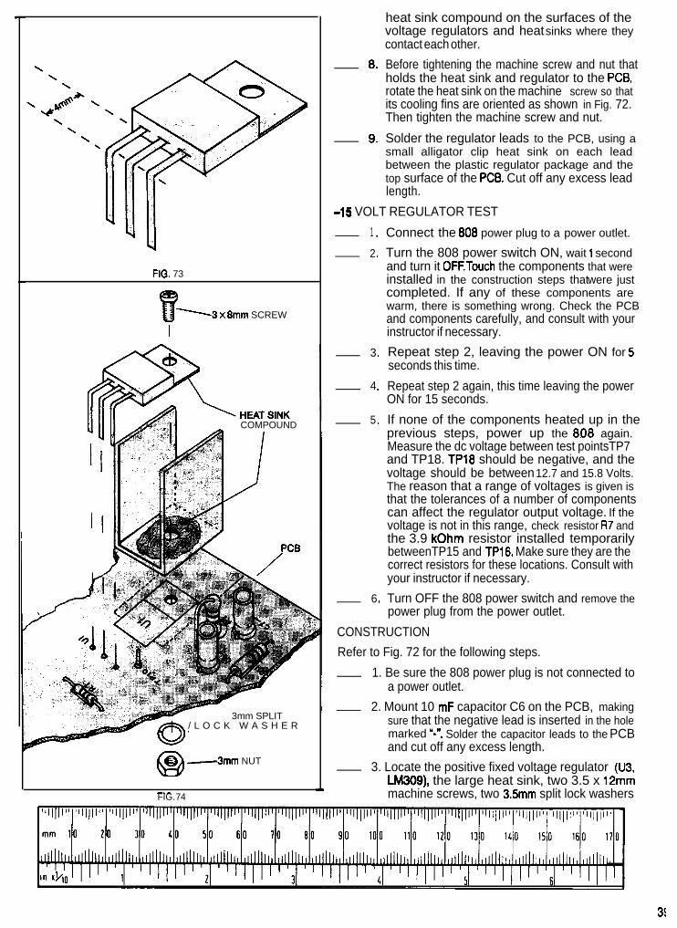
FIG. 73
!r13 x 8mm SCREW
I
COMPOUND
3mm SPLIT/ L O C K W A S H E R
Qe -3mm NUT
FIG. 74
heat sink compound on the surfaces of thevoltage regulators and heat sinks where theycontact each other.
Before tightening the machine screw and nut thatholds the heat sink and regulator to the PCBrotate the heat sink on the machine screw so thatits cooling fins are oriented as shown in Fig. 72.Then tighten the machine screw and nut.
Solder the regulator leads to the PCB, using asmall alligator clip heat sink on each leadbetween the plastic regulator package and thetop surface of the PCB. Cut off any excess leadlength.
-15 VOLT REGULATOR TEST
1 .
2 .
3 .
4 .
5 .
6 .
Connect the 608 power plug to a power outlet.
Turn the 808 power switch ON, wait 1 secondand turn it OFFTouch the components that wereinstalled in the construction steps that were justcompleted. If any of these components arewarm, there is something wrong. Check the PCBand components carefully, and consult with yourinstructor if necessary.
Repeat step 2, leaving the power ON for 5seconds this time.
Repeat step 2 again, this time leaving the powerON for 15 seconds.
If none of the components heated up in theprevious steps, power up the 8.06 again.Measure the dc voltage between test pointsTP7and TP18. TPl8 should be negative, and thevoltage should be between 12.7 and 15.8 Volts.The reason that a range of voltages is given isthat the tolerances of a number of componentscan affect the regulator output voltage. If thevoltage is not in this range, check resistor R7 andthe 3.9 kOhm resistor installed temporarilybetweenTP15 and TPl6. Make sure they are thecorrect resistors for these locations. Consult withyour instructor if necessary.
Turn OFF the 808 power switch and remove thepower plug from the power outlet.
CONSTRUCTION
Refer to Fig. 72 for the following steps.
1. Be sure the 808 power plug is not connected toa power outlet.
2. Mount 10 mF capacitor C6 on the PCB, makingsure that the negative lead is inserted in the holemarked “-‘I Solder the capacitor leads to the PCBand cut off any excess length.
3. Locate the positive fixed voltage regulator (U3,LM309), the large heat sink, two 3.5 x 12mmmachine screws, two 3.5mm split lock washers
3(.

and two 35mm nuts.
4. Refer to Fig. 75. Mount the LM3OQ regulator andheat sink on the PCB, using the hardware called - 3 .out in step 3. Graymark r8commends the use ofheat sink compound on the surfaces of the ’voltage regulators and heat sinks where they
4 .
contact each other. Be sure that the largermachine screws (35mm diameter) are us8d to - 5 .fasten the IC and heat sink to the PCB. If you usethe smaller 3mm diameter screws for thispurpose, it is possible for the heat sink to shortto the IC leads.
5. Solder the regulator leads to the PCB. Cut off anyexcess lead length.
+5 VOLT REGUMTOR TEST
1. Conn8ct th8 808 power plug to a power outlet.
2. Turn th8 808 power switch ON, wait 1 s8cond-
6 .and turn it OFETouch the components that wereinstalled in the construction steps that were justcompleted. If any of these components arewarm, there is sumething wrong. Check the PCB
and components carefully, and consult with yourinstructor if necessary.
Repeat step 2, leaving the power ON for 5s8conds this time.
Rep8at step 2 again, this time leaving the powerON for 15 seconds.
If none of the components heated up in theprevious steps, power up the 808 again.Measure the dc voltage between* test pointsTPi 9 and TP7.TPlQ should be positive, and thevoltage should be between 4.6 and 5.4 Volts.This range of voltages allows for the specifiedoutput voltage tolerance (4.7 to 5.3 Volts), plusapproximately 2 % measurement error. lf thevoltage is not in this range, check your workcarefully, and consult with your instructor ifn8cessarym
Turn OFF the 808 power switch and remove thepower plug from the power outlet.
FIG. 75
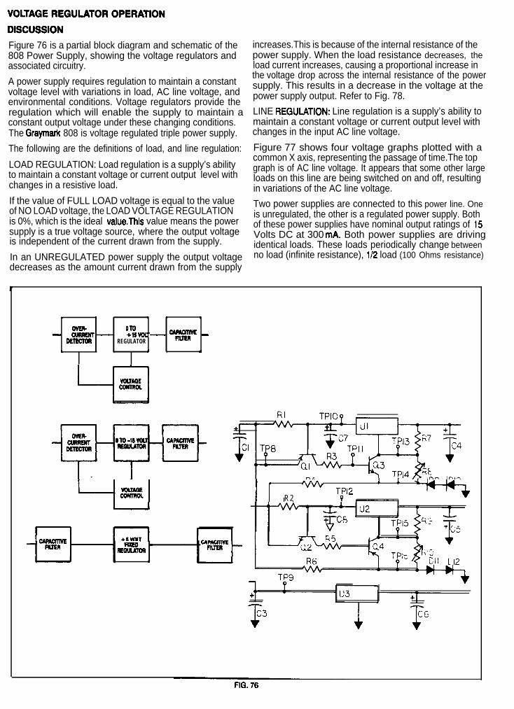
Figure 76 is a partial block diagram and schematic of the808 Power Supply, showing the voltage regulators andassociated circuitry.
A power supply requires regulation to maintain a constantvoltage level with variations in load, AC line voltage, andenvironmental conditions. Voltage regulators provide theregulation which will enable the supply to maintain aconstant output voltage under these changing conditions.The Graymark 808 is voltage regulated triple power supply.
The following are the definitions of load, and line regulation:
LOAD REGULATION: Load regulation is a supply’s abilityto maintain a constant voltage or current output level withchanges in a resistive load.
increases.This is because of the internal resistance of thepower supply. When the load resistance decreases, theload current increases, causing a proportional increase inthe voltage drop across the internal resistance of the powersupply. This results in a decrease in the voltage at thepower supply output. Refer to Fig. 78.
LINE REGUIATION: Line regulation is a supply’s ability tomaintain a constant voltage or current output level withchanges in the input AC line voltage.
Figure 77 shows four voltage graphs plotted with acommon X axis, representing the passage of time.The topgraph is of AC line voltage. It appears that some other largeloads on this line are being switched on and off, resultingin variations of the AC line voltage.
If the value of FULL LOAD voltage is equal to the valueof NO LOAD voltage, the LOAD VOLTAGE REGULATION
Two power supplies are connected to this power line. One
is 0%, which is the ideal value.This value means the poweris unregulated, the other is a regulated power supply. Both
supply is a true voltage source, where the output voltageof these power supplies have nominal output ratings of 15
is independent of the current drawn from the supply.Volts DC at 300 mA. Both power supplies are drivingidentical loads. These loads periodically change between
In an UNREGULATED power supply the output voltage no load (infinite resistance), 1/2 load (100 Ohms resistance)decreases as the amount current drawn from the supply
. + 4 I 4
OVER OTO- CURRENT ’ ’ +15vou ’ ’ YiEF -
DETECTOR REGULATOR
6 . , + , -4
I - I I I,
T?l2I I R2 ?
--
fiXED bREGULATOR
. .
FIG. 76

and full load (50 Ohms resistance).The changing condition following formula:of these loads is shown by the second graph.
% toad “*ItageFigure 78 is the equivalent circuits of the unregulated and regulation =
Vout (no load) - Vout (full load) x 1 o.
the regulated power supplies. The boxes labeled INPUT IVout (full load)
POWER CONDITIONING represent the input circuitry, At the nominal line input voltage of 115 Volts.power transformer, rectifiers and input filters. The resistorslabeled Ri”t represent all the losses and resistances in the
VOJ (no load) occurs at the point on the Unregulated Power
components mentioned above.Supply Output graph that is marked with the letter A.
Vout (full load) occurs at the point marked with the letter B.In the equivalent circuit of the regulated power supply, thevariable resistor labeled R&r represents the Darlingtontransistor in the voltage regulator that controls the currentthat flows through the regulator to the load resistors. Theload resistors are shown with push-button switches,ganged together between the two loads. With this setup,the load conditions shown in the second graph could beduplicated by manipulating the switches.
Calculate the % load voltage regulation for this powersupply and write your answer in the space provided.
OO/
The bottom graph in Fig. 77, shows the regulated powersupply output voltageThe little “glitches’ appearing on thisgraph indicate that the voltage regulator cannot instantlycompensate for input voltage and load changes. Moreabout that later.How voltage regulators actually work will be discussed in
more detail a little later. Right now we just want to see thedifferences in the output voltages of unregulated andregulated power supplies with varying line input voltagesand loads.
The third graph from the top shows the output voltage of theunregulated power supply. What is the worst case voltage
variation in Volts?
Most real life regulators won’t provide the zero percentregulation shown on the graph, but the voltage regulatorsin your Graymark 808 Power Supply will provideconsiderably better than 1% combined line and loadregulation.
Figure 79 shows the schematic diagram of the LM317voltage regulator. Transistors, resistors, Zener diodes and
Under what conditions is the output voltage the highest? capacitors are formed in a small piece of silicon, oftencalled a “chip”.To help understand how a voltage regulator
Input line. Load. functions, we will be using a functional schematic, which
Under what conditions is the output voltage the lowest?is shown in Fig. 80.
Input line. Load. The operation of all three of the IC voltage regulators usedin the Graymark 808 Power Supply is based on the same
To calculate the % load voltage regulation, use the general principles. The following discussion applies to the
INPUTLINE 115
VOLTAGE
FULL LOAD(50 OHMS)
112 LOAD‘OAD (100 OHMS)
NO LOAD
23
21UNREGULATED
POWER SUPPLY lgOUTPUT (VOLTS) 17
17REGULATED
POWER SUPPLY 15OUTPUT (VOLTS) l3
FIG. 77
42

LM309, the LM317 and the LM337. The LM337 is anegative regulator,that is, its input and output voltages arenegative in respect to ground. This results in differentpolarities inside the IC, but it operates according to thesame principles as the LM309 and LM317.
UNREGUUKTED POWER SUPPLY
REGUIATED POWER SUPPLY
FIG. 78
REPRINED WITH PERMISSION OF NATIONAL SEMICONDUCTOR COF?PORAT/ON
FIG. 79
INPUT,
DARLINGTONTRANSISTOR
------1
0 OUTPUT
The two overlapping circles and the arrow in the upper lefthand corner of the schematic form the symbol for a currentsource. A current source will pass a constant current, in thiscase 50 uA, despite variations of the voltage appearingacross its terminals. This current source provides aconstant current for the I .25 Volt Zener diode that suppliesthe reference voltage for the regulator.
Resistors R* and Rb form a voltage divider. Rb has threetimes the resistance in Ohms of Ra, so when the voltageat the regulator output terminal is 5 Volts, the voltage at thejunction of R* and Rb is 1.25 Volts.The operational amplifier(op amp) compares this portion of output voltage of theregulator to the 1.25 Volt reference voltage. As long as thetwo input terminals of the op amp are at the same voltage,there is very little current flowing either into or out of the opamp output terminal.
The adjustable voltage regulators are a little different. Raand Rb are external to the regulatorsThis will be discussedlater in the EXTERNAL CONTROL AND PROTECTIONCIRCUITRY section.
If we increase the voltage regulator load by connecting aresistor between the regulator output and ground, theadditional current flowing through the regulator will causethe output voltage to drop below 5 Volts.The voltage at theop amp input terminal marked with the minus sign dropsas well. The op amp responds to this input change bymoving its output in a positive direction, causing anincrease in the base current of the Darlington transistorshown at the right side of Fig. 80.
The Darlington transistor is named after the person whoinvented this particular way of connecting two transistorsand a resistor together to form the equivalent of onetransistor. A Darlington transistor requires very little baseinput current to control the collector output current, and canrespond to rapid changes of the base current.
A transistor can be thought of as a valve that controls theflow of electrons, that is, the current in a circuit. The “valvehandle” of the transistor is its base. The amount of currentflowing through the transistor from emitter to collector iscontrolled by a much smaller current flowing from theemitter to the base.
Another way of looking at a transistor is to consider it as avariable resistor, where an increase in the base currentcauses a decrease in the resistance.
At this point, the output of the voltage regulator is below 5Volts because an additional load resistor was connectedbetween its output terminal and ground. This loweredoutput voltage caused the voltage at the inverting input ofthe op amp to become lower as well.The op amp respondsto this input voltage change by by moving its output in apositive direction, increasing the base current of theDarlington transistor.
The resulting decrease of resistance between theDarlington transistor’s emitter and collector causes anincrease in the current flowing through the voltageregulator and the load resistors. In accordance with Ohm’slaw, (voltage = current x resistance), the output voltage ofthe voltage regulator heads back up to 5 Volts.
Figure 81 shows the effects of connecting a load resistorto the output of a voltage regulator. The conditions shownin the right portion of the figure occur after the load resistor
FIG. 80
43

is connected, but before the voltage regulator. is able to Equipment: DVM or DMMcompensate for this change in load resistance.
It takes much longer to describe the operation of a voltage 1 .regulator than it takes for the regulator to operate.There issome time delay from the instant that a load change orinput voltage change takes place and causes the outputvoltage to change until the voltage regulator is able to - 2 .
compensate and restore the correct output voltage. Thistime delay occurs mostly in the op amp and Darlington 3 .transistor circuitry. Figure 82 is from the LM309specification sheets, and illustrates the time required forthe LM309 regulator to respond to a load change. Noticethat it is a very short time, about 1 micro second.
The output filter capacitor for the fixed supply, C6, reduces 4 .the amplitude of these voltage spikes. C6 has acapacitance of 10 mF It does not need to have a large - 5 .
capacitance like C3, the input filter capacitor, because ofthe short periods of time it must provide or absorb electricalenergy to keep the output voltage constant. Look again atFig. 63.The time that the input filter capacitor must provideelectrical energy is about 6 milliseconds, which is 6000times as long as 1 microsecond.
The circuitry symbolized by the rectangle labeledPROTECTION CIRCUITRY can divert the op amp outputcurrent away from the base of the Darlington transistor.Normally, when the op amp output moves in the positivedirection, we want to increase the current flowing throughthe voltage regulator and load resistor. But when thiscurrent reaches the maximum value the regulator cansafely handle, we don’t want it to increase any more.
The voltage across resistor Rc is directly proportional to thecurrent flowing through it. (Ohm’s law again, voltage =current x resistance. As the output current of the regulatorincreases, the voltage across R= increases as well. Whenthis voltage reaches a level that indicates the maximumsafe current is flowing, the protection circuitry begins todivert current away from the Darlington transistor base.
OVERCURRENT PROTECTION EXPERIENCE
6 .
7 .
Clip Lead
Be sure that the 808 power plug is NOTconnected to a power outlet. Refer to Fig. 83 forthe following steps.
Remove the 1.5 kOhm test resistor which issoldered toTP7 and TP9.
Connect the positive meter lead toTP8 and thenegative meter lead toTP1 O.The meter will readthe voltage across the current sensing resistorRl. Set the meter range selector to read a DCvoltage of 2.5 Volts.
Connect the 808 power plug to a power outlet.
Turn the 808 power switch ON. While observingthe meter, connect the clip lead from TP7 toTP17. This is a short circuit across the positivevariable regulator, LM317. This represents aheavy overload for the power transformer andcurrent sensing resistor Rl . Read the meter andquickly remove the clip lead. Write down the
meter reading here. Volts
Using Ohm’s law, calculate how much current isflowing through the regulator.
Amps. Notice thatwhen using a 1 Ohm current sensing resistor,The voltage across the resistor in Volts is thesame as the current flowing through the resistorin Amps. The same correspondence occurswhen voltage is in millivolts, the current is thenin milliamps. How does the current youmeasured compare to the value given on theNational Semiconductor Electrical Characteris-tics specification sheet for the LM317?
Turn OFF the 808 power switch and remove thepower plug from the power outlet. Disconnect theclip lead and the meter test leads.
Purpose: To observe the operation of the internal Just how hot a voltage regulator becomes when it isovercurrent limiting function of a voltage regulatotz operating depends on a number of variables. The input
POSITIVEINI+*FROM
FILTER
POSITIVEINPUTFROM
FILTEII CURRENT
_WllA WILL INCREASE. I3 JU
vw’aw.
--t/h I \ DARLINGTONTRANSISTOR I1
11.25V
RESISTANCEWILLDECREASE/
RESIS’KANCEIS STABLEOP
A+
7 \’1.25V
1.25V
I! /480V
-()OUTPUT
LOADRESISTOR
NEGATIVEl%PUToFROM
FILTER
LOADRESISTOR
NEGATIVE INPUT
GND FROM FILTER GND
FIG. 8144

LOAD TRANSIENT RESPONSE
0 1 2 3 4 5 6TwiE bd
EPm/7Ell WIW PEaMss~uN OF u4mNAL sEM/coNmJcmR coRPoRAnoN
FIG. 82
FIG. 83
voltage, along with the output current and voltage, affectthe amount of power that the regulator has to dissipate.Thesize of the heat sink and the amount air flow around itaffects how much the temperature of the regulator mustrise to dissipate this power.
If a voltage regulator gets too hot, it will be damaged, eventhough the current flowing through it is within safe limits.
The protection circuitry on the voltage regulator chipincludes a temperature sensor. When the chip temperaturereaches its maximum safe limit, the protection circuitrybegins to divert some of the op amp output current from theDarlington transistor base, just as it did when the regulatoroutput current reached its maximum safe value, as wediscussed earlier.
OVER TEMPERATURE PROTECTION
DISCUSSION
To force the LM317 voltage regulator into its overtemperature protection mode without risking damage toother power supply components, the regulator will beoperated without a heat sink attached while supplyingapproximately the maximum rated current of the powersupply. The 50 Ohm 5 Watt test resistor that will be usedfor a load draws between 254 and 316 mA with theregulator output voltage between 12.7 and 15.8 Volts. The3.9 kOhm test resistor that was installed in place of variableresistor R8 sets the regulator output within this range. If youwish to, refer back to step 5 of the + 15 VOLT REGUMTORTEST
TEMPERATURE PROTECTION EXPERIENCE
Purpose: To observe a voltage regulator and its outputwhen if is in the over temperature protection mode.
Equipment: OscilloscopeVOM or DMM50 Ohm 5 Watt Test ResistorDrinking Straw
1. Be sure that the 808 power plug is NOTconnected to a power outlet.
Refer to Fig. 84 for the following steps.
2 .
3.
4 .
5 .
6 .
Temporarily remove the mounting hardware andheat sink for the LM317 regulator from the PCB*
Solder the 50 Ohm test resistor leads toTP7 andTPl7.
Connect the ground lead of the scope and thenegative lead of the DVM or the DMM to the testresistor lead going to TP7. Connect the scopeprobe and the positive lead of the meter to thetest resistor lead going toTPl7. Adjust the meterand scope to read and display a 15 Volt DCsignal.
Connect the 808 power plug to a power outlet.
Turn the 808 power switch ON. Watch the meterand scope display. Depending on the ambienttemperature and the power line voltage, it maytake a minute or more for the voltage regulator toreach the temperature at which the over

PtiOBE
50 OHM 5 WAT T&T RESISTOR
FIG. 84temperature protection circuitry begins tooperate. When the over temperature circuit isactivated, the voltage across the test resistor willbegin to drop. Wait approximately 1/2 minute
longer. What is the meter reading? - Volts
7. While watching the meter and scope display, usethe drinking straw to blow on the LM3l7regulator. What happens?
8. Turn OFF the 808 power switch and remove thepower plug from the power outlet. Disconnect thetest equipment and unsolder the test resistor.Replace the heat sink and mounting hardwarethat was removed in step 2.
This completes the TEMPERATURE PROTECTIONEXPERIENCE. Have your instructor initial your progresschart.
46
EXTERNAL CONTROL AND PROTECTIONCIRCUITRY SECTIONVOLTAGE CONTROL
DISCUSSION
Figure 85 is a partial block diagram and schematic of theGraymark 808 Power Supply, with the external voltagecontrol circuitry highlighted.
Figure 86 is a functional diagram of the positive adjustableregulator and its external voltage control circuitry. Thenegative adjustable regulator is similar, but with reversedvoltage polarities. Comparing this schematic with thefunctional schematic of the fixed voltage regulator shownin Fig. 80, we see that resistors Ra and Rb are now outsidethe regulator, and that the ground terminal has become theadjustment terminal.
Because the adjustment terminal Is the control Input of thevoltage regulator, the current necessary to operate the opamp and protection circuitry inside the regulator must flowfrom the input terminal,through the regulator circuitry andthrough the output terminal.This is why there needs to besome output current flowing whenever the regulator isoperating. The bleeder resistor and the voltage controlresistors, Ra and Rb, provide the load needed to cause thiscurrent flow.
ADJUSTMENT VOLTAGE EXPERIENCE
The voltage that is applied to the adjustment terminal of avoltage regulator determines the output voltage of thatregulator. The op amp inside the regulator adjusts theresistance of the Darlington transistor so that the voltageat the op amp’s inverting input (marked with a minus (0)sign) is the same as the voltage at its non-inverting input(marked with a plus ( + ) sign).
Purpose: To demonstrate how an adjustable voltageregulator3 output responds to different voltages at theadjustment terminal.Equipment: VOM or DMM
Clip Lead1. Be sure the 808 power plug is not connected to
a power outlet.
Refer to Fig. 87 for the following steps.
2 .
3 .
4 .
5 .
Connect the negative meter lead toTP 7 and thepositive meter lead toTP 17. Set the meter to arange that will read up to 20 Volts DC.
Connect the 808 power plug to an outlet and turnthe power switch ON. Write the voltmeter readingdown in Fig. 88 in the “Output Voltage” columnand the Clip Lead Connections “None” row (inthe box marked # 1). Move the negative meterlead toTP 13 and write the voltmeter reading inthe “Output to Adjustment Voltage Difference”column and the Clip Lead Connections “None”row (box # 2). Set the meter range selector to alower range if necessary for an accurate reading.
Connect the clip lead toTP 13 and TP 2. Write themeter reading down in box # 3. Move thenegative meter lead back to TP 7 and write themeter reading down in box # 4.
Disconnect the negative meter lead from TP 7

RI TPIC? -
FIG. 85
INPUT
DARLINGTONTRANSISTOR
r ~~~~~.
7 4 VOLTSUNREGUlATED l- I
6 ADJUSTMENT
COMMON t
-24 VOLTS IUNREGULATED
FIG. 86 FIG. 87
while you change one end of the clip lead fromTP 2 to TP 14. Reconnect the negative meterlead to TP 7 and write the meter reading in box# 5. Move the the negative meter lead from TP7 to TP 13 and write down the meter reading inbox # 6.
Notice that while the output voltage changedwhen the adjustment terminal of the voltageregulator was connected to different voltages,the output-to-adjustment voltage differenceremained the same.The op amp was controllingthe Darlington transistor resistance so that theop amp’s input terminals remained at the samevoltage- The 1.25 Volts across the output and
regulator output voltages.
When the adjustment terminal is connected toground, the regulator output voltage is 1.25Volts. To be able to adjust the output voltage to0 Volts, two diodes connected in series areforward biased by the unregulated negativesupply, through R4. The exact voltage dropacross the diodes will vary with the currentflowing through them and their temperature, butit is approximately 1.4 Volts, or 0.7 Volts for eachdiode.This results in the variables supplies beingadjustable to and a little beyond zero Volts. Withthe voltage controls turned all the way down, the
adjustment terminals of the regulator is actually ,the voltage of the voltage reference inside the CLIP LEA0
regulator.WNNKTDNS
OUTPUFTM&JUSTMENTVOlTAGE VOLTAGE DIFFERENCE
NONE.
#l #2,Later, when you connect potentiometers R8 and TP13 TO TP?
##4 #3.
RlO to the PCB, they will control the adjustable TP13 TO Tfl4 #5, k#6FIG. 88
47
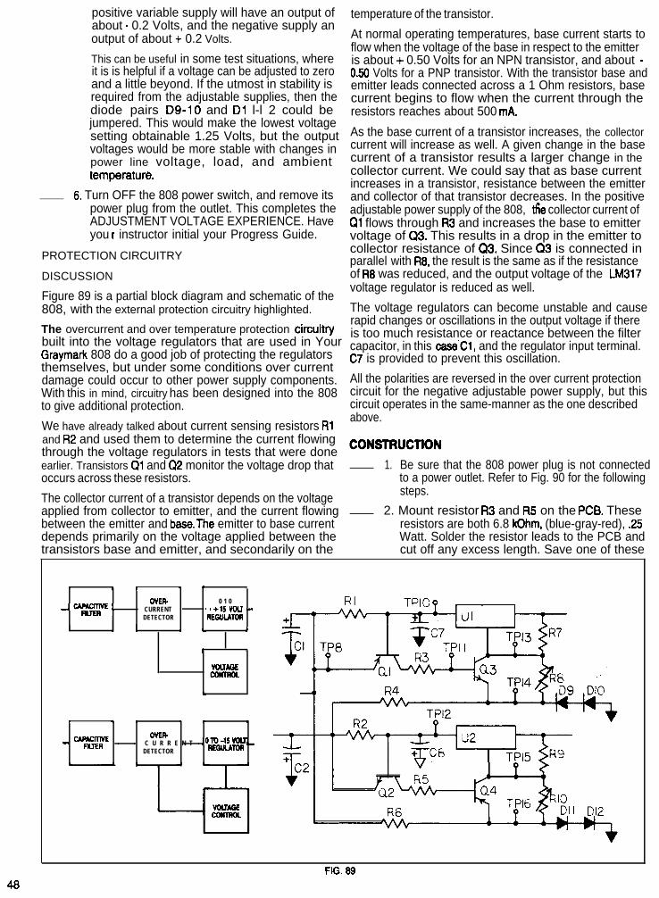
positive variable supply will have an output ofabout - 0.2 Volts, and the negative supply anoutput of about + 0.2 Volts.
This can be useful in some test situations, whereit is is helpful if a voltage can be adjusted to zeroand a little beyond. If the utmost in stability isrequired from the adjustable supplies, then thediode pairs D9-10 and Dl l-l 2 could bejumpered. This would make the lowest voltagesetting obtainable 1.25 Volts, but the outputvoltages would be more stable with changes inpower line voltage, load, and ambienttemperature.
6. Turn OFF the 808 power switch, and remove itspower plug from the outlet. This completes theADJUSTMENT VOLTAGE EXPERIENCE. Haveyou r instructor initial your Progress Guide.
PROTECTION CIRCUITRY
DISCUSSION
Figure 89 is a partial block diagram and schematic of the808, with the external protection circuitry highlighted.
The overcurrent and over temperature protection circuittybuilt into the voltage regulators that are used in YourGraymark 808 do a good job of protecting the regulatorsthemselves, but under some conditions over currentdamage could occur to other power supply components.With this in mind, circuitry has been designed into the 808to give additional protection.
We have already talked about current sensing resistors Rland R2 and used them to determine the current flowingthrough the voltage regulators in tests that were doneearlier. Transistors Ql and Q2 monitor the voltage drop thatoccurs across these resistors.
The collector current of a transistor depends on the voltageapplied from collector to emitter, and the current flowingbetween the emitter and base.The emitter to base currentdepends primarily on the voltage applied between thetransistors base and emitter, and secondarily on the
temperature of the transistor.
At normal operating temperatures, base current starts toflow when the voltage of the base in respect to the emitteris about + 0.50 Volts for an NPN transistor, and about -050 Volts for a PNP transistor. With the transistor base andemitter leads connected across a 1 Ohm resistors, basecurrent begins to flow when the current through theresistors reaches about 500 mA.
As the base current of a transistor increases, the collectorcurrent will increase as well. A given change in the basecurrent of a transistor results a larger change in thecollector current. We could say that as base currentincreases in a transistor, resistance between the emitterand collector of that transistor decreases. In the positiveadjustable power supply of the 808, tl?e collector current ofQl flows through R3 and increases the base to emittervoltage of Q3. This results in a drop in the emitter tocollector resistance of Q3. Since Q3 is connected inparallel with R8, the result is the same as if the resistanceof R8 was reduced, and the output voltage of the LM317voltage regulator is reduced as well.
The voltage regulators can become unstable and causerapid changes or oscillations in the output voltage if thereis too much resistance or reactance between the filtercapacitor, in this case’C1, and the regulator input terminal.C7 is provided to prevent this oscillation.
All the polarities are reversed in the over current protectioncircuit for the negative adjustable power supply, but thiscircuit operates in the same-manner as the one describedabove.
1. Be sure that the 808 power plug is not connectedto a power outlet. Refer to Fig. 90 for the followingsteps.
2. Mount resistor R3 and R5 on the PCB. Theseresistors are both 6.8 kQhm, (blue-gray-red), .25Watt. Solder the resistor leads to the PCB andcut off any excess length. Save one of these
. t t 4 . l
_-E, ,
OVER- 0 1 0
FIUERCURRENT I 3 +lS VOU -DETECTOR REGULAXM
1 1 \ & 4
B l
VouhGE.
* 4 \ , . ,
OVER-- FILTER ’ ’ C U R R E N T 1 ~om-‘sw-
DETECTOR REGUlAmR
48FIG. 89
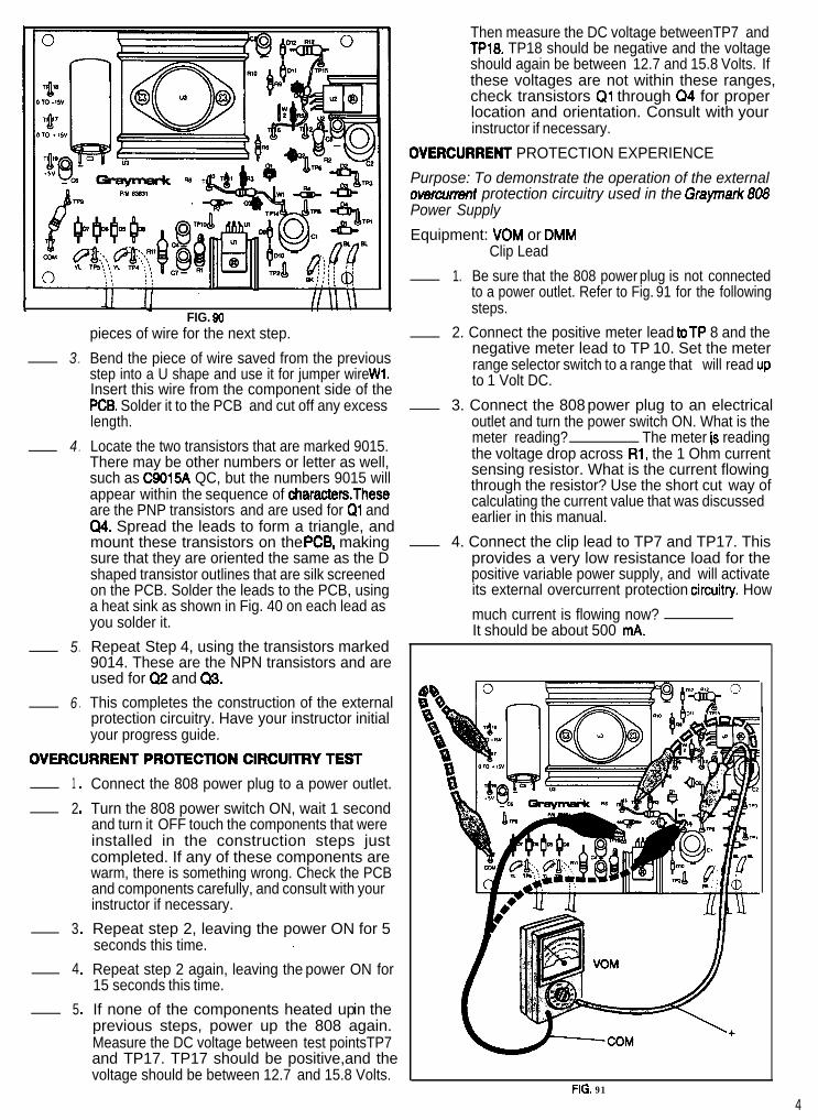
3 .
4 .
5 .
6 .
FIG. 90pieces of wire for the next step.
Bend the piece of wire saved from the previousstep into a U shape and use it for jumper wire Wl .Insert this wire from the component side of thePCB. Solder it to the PCB and cut off any excesslength.
Locate the two transistors that are marked 9015.There may be other numbers or letter as well,such as CQOl5A QC, but the numbers 9015 willappear within the sequence of charactersTheseare the PNP transistors and are used for Ql andC4. Spread the leads to form a triangle, andmount these transistors on the PCB, makingsure that they are oriented the same as the Dshaped transistor outlines that are silk screenedon the PCB. Solder the leads to the PCB, usinga heat sink as shown in Fig. 40 on each lead asyou solder it.
Repeat Step 4, using the transistors marked9014. These are the NPN transistors and areused for Q2 and Q3.
This completes the construction of the externalprotection circuitry. Have your instructor initialyour progress guide.
1 .
2 .
3 .
4 .
5 .
Connect the 808 power plug to a power outlet.
Turn the 808 power switch ON, wait 1 secondand turn it OFF touch the components that wereinstalled in the construction steps justcompleted. If any of these components arewarm, there is something wrong. Check the PCBand components carefully, and consult with yourinstructor if necessary.
Repeat step 2, leaving the power ON for 5seconds this time. .
Repeat step 2 again, leaving the power ON for15 seconds this time.
If none of the components heated up in theprevious steps, power up the 808 again.Measure the DC voltage between test pointsTP7and TP17. TP17 should be positive,and thevoltage should be between 12.7 and 15.8 Volts.
Then measure the DC voltage betweenTP7 andTPl8. TP18 should be negative and the voltageshould again be between 12.7 and 15.8 Volts. Ifthese voltages are not within these ranges,check transistors Ql through CJ4 for properlocation and orientation. Consult with yourinstructor if necessary.
OVERCURRENT PROTECTION EXPERIENCE
Purpose: To demonstrate the operation of the externalovercurrent protection circuitry used in the Graymark 808Power Supply
Equipment: VOM or DMMClip Lead
1. Be sure that the 808 power plug is not connectedto a power outlet. Refer to Fig. 91 for the followingsteps.
2. Connect the positive meter lead toTP 8 and thenegative meter lead to TP 10. Set the meterrange selector switch to a range that will read upto 1 Volt DC.
3. Connect the 808 power plug to an electricaloutlet and turn the power switch ON. What is themeter reading? The meter is readingthe voltage drop across Rl, the 1 Ohm currentsensing resistor. What is the current flowingthrough the resistor? Use the short cut way ofcalculating the current value that was discussedearlier in this manual.
4. Connect the clip lead to TP7 and TP17. Thisprovides a very low resistance load for thepositive variable power supply, and will activateits external overcurrent protection circuitv. How
much current is flowing now?It should be about 500 mA.
FIG. 914

BLACK 18 GAUGE
GREEN 2
5. Disconnect both meter leads and reconnect the be used.
6 .
positive meter lead to TP 11 and the negativelead toTP 14.The meter will now read the voltagebetween the emitter and base of Q3.What is the
meter reading now?(The clip lead should still be connected toTP 7and TP 17.)
Remove the clip lead fromTP7 and TP 17. Whatis the voltage across the base / emitter junction
of Q3 now?
VOLTAGE CONTROL OPERATIONALTESTPupose: To determine that the external voltage controlcircuitry is working properly
In step 5 the voltage across the base / emitterjunction was more than 0.5 Volts, and currentwas flowing from the collector to the emitter. Inthis step the voltage from the base to the emitterof Q3 was very low, so there was almost nocurrent flowing from the collector to the emitter.
7. Turn OFF the 808 power switch and disconnectthe power plug from the power outlet. Removethe test clip and meter leads. Remove the two 3.9kOhm test resistors from TPI 3, TP14, TPI 5 andTP16.
6. Repeat step 5, this time using the two red wiresand the second potentiometer.
7. Insert the free ends of the green wires in the PCBholes that are nearest to the silk screeneddesignation “RlO”. Solder the wires to the PCBand cut off any excess length. It doesn’t matterwhich of the two wires goes into which of the twoholes.
8. Repeat step 7, this time using the free ends of thetwo red wires and the two holes on the PCBclosest to the designation “R8”.
1 .
CONSTRUCTION
- 1.
2 .
3 .
- 4.
5.
Be sure that the 808 power plug is not connectedto a power outlet. Refer to Fig. 92 for the following - - 2 .
steps.
Cut two 200mm pieces of green 22 gauge wireand strip 6mm of insulation from all four ends.Twist the exposed strands of fine wire togetheron each end and tin them. 3 .
Repeat step 2, cutting and preparing two 175mmpieces of red 22 gauge wire.
Locate the two 5 kOhm potentiometers. Bend thesmall metal tab on each potentiometer as shownin Fig. 93 so that it won’t interfere when thepotentiometer is mounted on the cabinet top. _ 4 .
Connect and solder the two green wiresprepared in step 2 to one of the potentiometers _ 5 .as shown in Fig. 93. It is important that thecorrect solder terminals of the variable resistors
During this test be careful not to let the terminalsof the potentiometers touch the PCB or any of thecomponents. Rotate the control shafts of bothpotentiometers to the full counter clockwiseposition. Adjust the range selector of your VOMor DMM to measure up to 20 Volts DC. Connectthe negative meter lead to TP7. Connect thepositive meter lead to TPl7.
Power up the 808. The voltmeter should readbetween 0 and - 0.3 Volts. Rotate the Shaft of thepotentiometer connected to the red wires to thefull clockwise position.The voltmeter should nowread between 15.5 and 20 Volts.
Remove the voltmeter leads fromTP17 and TP7.Reconnect the positive meter lead toTP7 and theNegative lead toTPl8.The voltmeter should readbetween 0 and + 0.3 Volts. Rotate the shaft ofthe potentiometer connected to the green wiresto the full clockwise position. The meter shouldnow read between 15.5 and 20 Volts.
Turn OFF the 808 power switch and disconnectthe power plug from the power outlet.
This completes the VOLTAGE CONTROLOPERATIONAL TEST Have your instructorinitial your progress guide.
50

FINAL PCB ASSEMBLY1. Be sure that the 808 power plug is NOT
connected to a power outlet. Refer to Fig. 92 forthe following steps.
2. Locate the four 15Omm lengths of 18 gauge wire.strip 6mm of insulation from each end of each ofthe four wires. Twist the fine strands of exposedwire on each of the ends together and tin them.Form one of the tinned ends of each of the wiresinto a hook shape with a long nose pliers.Connect and solder these hooked wire ends tothe following test points on the PCB.
- A. The black wire to TP 7.
- B. The red wire to TP 19.
- C. The orange wire to TP 17.
_ D, The gray wire to TP 18.
3. Cut a 1 OOmm piece of green 22 gauge wire. Strip6mm of insulation from each end.Twist?he smallstrands of wire together, and tin both ends.
4. Connect and solder the 3.5mm solder lug to oneend of the green wire that you prepared in theprevious step. Connect and solder the other endof this wire to the PCB. Use the unmarked holenear TP 7. Cut off any excess wire.
5. This completes the FINAL PCB ASSEMBLY.Have your instructor initial your progress guide.
CABINET ASSEMBLY
CAUTION!Be sure that the AC Cord is NOT pluggedinto an electrical outlet during this CabinetAssem biy Section.
1. Mount two rubber feet to one end of the cabinetbottom, using two 3 x 8mm self-tapping screws.Refer to Fig. 94.
2. Repeat the previous step for the other end of thecabinet bottom.
3. Remove the protective plastic from thebreadboard.
4. Place the cabinet top face up on your work
BENDTAB 90’
\
FIG. 93
3x9mmSELF-TAPPING SCREWS
-.- -FIG. 94
surface, so the printing on the cabirnet top isreadable.

5. Position the breadboard on the cabinet top, sothe printing on the breadboard is readable. Whileholding the breadboard in place, turn the cabinettop over.
Refer to Fig. 95 for the following steps.
6-0
7-’
Refer to
8-*
9-0
10 .
11.
12 .
13 .
14 .
Attach the breadboard to the cabinet top usingeight 2.6 x 5mm self-tapping screws. Do notover tighten the screws.
Attach the breadboard bus strip to the cabinettop using two 2.6 x 5mm self-tapping screws. Donot over tighten the screws.
Fig. 96 for the following steps.’
Position the transformer so the side with the twowhite wires is next to the cabinet side. Mount thetransformer to the cabinet bottom using two 3 x8mm machine screws, two 3mm flat washers,two 3mm lockwashers, and two 3mm nuts. Placethe solder lug which is attached to the greenwire from the PCB between the transformer andthe cabinet bottom as shown in Fig. 96. Thiswire provides an electrical connection betweenCommon (ground) on the PCB and the metalcabinet.
Unscrew and remove the four screws which areholding the standoffs at each corner of the PCB.
Using the screws, standoffs and nuts removed inthe previous step, mount the PCB to the cabinetbottom. Place four 3mm lockwashers betweenthe top of the PCB and the two 3mm nuts andthe two long standoffs. Position the PCB so thatIC Ul is next to the transformer.
Connect and solder the black wire from TP7 tothe solder lug on the black binding post whichwas installed on the cabinet top earlier, Cut offany excess wire that sticks out beyond thesolder lug.
Repeat Step 11, connecting the red wire fromTPl9 to the red + 5V binding post.
2.6 x 5mm SELF-TAPPING SCREWS(10 PLACES)
FIG. 95
15. Place a 7mm lo&washer over the threadedbushing of the potentiometer which is connectedto the PCB with two green wires. Mount thepotentiometer in the hole in the cabinet topmarked 0 to AS/, using a 7mm flat washer andhex nut.
Repeat Step 11, connecting the orange wirefrom TP17 to the red 0 to +15V binding post. 16. Repeat the prev ious s tep us ing the
Repeat Step 11, connecting the gray wire frompotentiometer connected to the PCB with two
TP18 to the red 0 to -15V binding post.red wires, mounting it in the hole marked 0 to+15v.

0
0
LOCKWASHERS /
1 w 4 0 m m
-a
+ ’ esFIG. 96
FLATWASHERS
53

FIG. 97
FIG. 98
54

Refer to Fig. 97 for the following steps. Refer to Fig. 98 for the following steps.
17 . Place the cabinet bottom on your work surface 22,as shown in Fig. 97.
18 . Make sure that all four brackets are lined upperpendicular with ‘the cabinet top beforeproceeding. 23 .
19 . Hold the cabinet top so that it can be folded ontothe cabinet bottom like a hinge. Carefullyposition all wires so that they will not be pinchedbetween any metal or other parts when the 24- *cabinet top is assembled to the cabinet bottom.
20 a Gently lower the cabinet top onto the cabinetbottom. Observe the wires to be sure they arenot pinched between any parts.
2~.
21. Once the cabinet top is positioned firmly onto the -26l
cabinet bottom, hold the two cabinet halvestightly together while you turn the unit over. 27- l
Continue to hold the cabinet tightly together.28 .
While holding the cabinet together, install four(4) 3 x 8mm screws with 3mm lo&washers intothe four (4) holes in the bottom of the cabinet-
IGHTEN THES C -.
Install three (3) 3 x 8mm screws with 3mmlockwashers into the three holes on the left sideof the cab inet . DO NOmAEzGlWYS*
Install three (3) 3 x 8mm screws with 3mmlockwashers into the three (3) holes on the leftside of the cabinet. DO NOT Tm THESXEIE
Tighten the screws installed in Step 22.
Tighten the screws installed in Step 23.
Tighten the screws installed in Step 24.
This completes construction of your GraymarkModel 808 Triple Power Supply/Bread board.
55

FINAL TEST
Pupuse: To verify that th6 three power supplies workproperly after cabinet assembly
Equipment: VOM or DMM
1 l
2 .
3 .
4 .
5 *
6 .
- 7.
8 .
9 .
10.
11 .
12.
13.
14 .
15.
16 .
17.
18 .
19 .
20 *
50 Ohm 5 Watt Resistor
Connect one end of the 50 Ohm resistor to theCOM terminal. Connect the other end to the + 5VDC terminal.
Adjust the meter to read +5 VDC.
Connect the negative meter lead to the COMterminal.
Connect the positive meter lead to the + 5 VDCterminal.
Connect the 808 power plug to an electricaloutlet and turn the power switch ON.
The voltmeter should read between 4.7 and 5.3Volts. If the voltage is correct, proceed to the nextstep. If it is not correct, STOP, turn power OFFand remove the power plug from the outlet.Then,check the resistor and meter connections. If allconnections are correct, you may have pinchedor broken a wire during the cabinet assembly.
Turn the power switch OFF
Adjust the DC Voltmeter to read + 15 VDC.
Disconnect the resistor lead and the positivemeter lead from the +5 VDC terminal.Reconnect both to the 0 to + 15 VDC terminal.
Turn the power switch ON.
Monitor the voltage while turning the adjustmentpotentiometer using a small screwdriver. Youshould be able to adjust the supply between 0and 15 Volts. If the voltage is correct, proceed tothe next step. If it is not correct, STOP, turn powerOFF and remove the power plug from the outlet.Then check the resistor and meter connections.If all connections are correct, you may havepinched or broken a wire during the cabinetassembly.
Turn the power switch OFF
Adjust the DC Voltmeter to read -15 VDC.
Disconnect the resistor lead from the 0 to + 15VDC terminal. Reconnect it to the 0 to -15 VDCterminal.
Disconnect both meter leads.
Adjust the meter to read + 15 VDC.
Connect the negative meter lead to the 0 to -15WC terminal.
Connect the positive meter lead to the COMterminal.
Turn the power switch ON.
Monitor the voltage while turning the adjustmentpotentiometer. You should be able to adjust thesupply between 0 and 15 Volts. You should be
21 .
22 .
23 .
able to adjust the supply between 0 and 15 Volts.If the voltage is correct, proceed to the next step.if it is not correct, STOP, turn power OFF andremove the power plug from the outlet. Thencheck the resistor and meter wnnections. If allwnnections are wrrect, you may have pinchedor broken a wire during the cabinet assembly.
Turn the power switch OFF
Disconnect the voltmeter and resistor from theModel 808.
This completes the Final Test.
OPERATIONThe Breadboard portion of your Model 808 is populatedwith 2,420 holes.The leads of electronic wmponents suchas integrated circuits, transistors, resistors and capacitors,as well as wires, can be inserted into these holes Byinserting electronic components and wires into theBreadboard, you can design and wnstruct experimental(prototype) circuits. Before you can use the Breadboard,however, you must understand how the 2,420 holes areinterwnnected.
The Breadboard is comprised of eight sections, five busstrip sections and threecomponent sections, as shown inFig 99. The bus strips are used to distribute or “bus”power and electronic signals to different areas of theBreadboard. The component sections are where theelectronic components are mounted.
Various wire sizes can be accommodated by theBreadboard, as well as the following component leads:
SIP and DIP Integrated Circuits1/8 to 1/2 Watt ResistorsMost CapacitorsMost Small Transistors
Bus Strips
Each of the five bus strips wntains four segments of 25holes each. Each segment is identified by a blue or redstripe printed next to the segment.The 25 holes which arenext to each stripe are connected together, so that a wireor component lead inserted into any of the 25 holes will beconnected to any wire or wmponent which is inserted intoany of the remaining 24 holes in that segment.
Component Sections
Each of the three component sections contains 128segments of five holes each.The segments are horizontalrows, and each segment is identified by a number (1 to 64)printed next to the segment.The five holes in the row nextto each number are wnnected together, so that a wire orcomponent lead inserted into any of the five holes will beconnected to any wire or wmponent which is inserted intoany of the remaining four holes in that segment.
In each wmponent section, for reference only, the columnsare identified by letters A, B, C, D & E, and F G, H, I & J.
A portion of the Breadboard is shown in Fig. 104 to illustrate

r .A6COt FGH I J
1 l o * * * l o o o o '
2 .e**. r l . . . . . 2
A6CDE FGHIJ
2 *mom* . . . . . Il..... 23 . . . ..I [.....3
1 . . . . . Ii..... 4
5 . . . ..I ].....5
3 .*...j I.....3
b4 . . . ..I I.....4
6 . . . . . Il..... 6
r . . . . . I I . . . . . 7
s Am..11 . . . . . 56 *me.. I I . . . . . 6
10 l l a a a u l l . . . 10
11 . . . ..I 1 l . . . . 1111 l me*m H am..* 1112 l m o * m l .*..~213mmm*m ****a 13 13*.e.* II .*...13
14.....1 [.....I.
16 . . . ..I ~.....1514****m I I l . l . . 14
19 . . . . . I I 0 a.. . 16
17 . . . ..I ~.....17
15 mm...1 lo..*.15
+ 5 VOLTS
Ra 3.9K
ABCOE-.I A6COE
1 *-
FGHIJ4ffB1
2
345
67
9
9
1011
12
13
14
15
19
17
19
19
20
21
22
23
2425
29
2r
29
2*
30
31
32
33
l
0
0
l
l
l
l
l
l
*
l
l
*
l
0
0
l
l
l
0
l
0
0
0
0
t
Rb 3.9K VOM
FIG. 1 0 0 FIG. 101L
57

ABCOE1 l *eme2 l l l l l
2 l . l l l
1 l l l l l
s l l l l l
b l l l l l
7 l l l l l
8 l e l l l
9 l l l l l
IO l l l l l
11 l l l l l
I? l l l l l
13 l l l l l
14 l l l l l
15 l l l 0 l
16 l l l l l
17 l o e e e
18 l l l l l
19 l l l l l
20 l l l l l
21 l l l l l
22 l e e e e13 l e e e e
t4 l l l l 025 l e e e e2b l l l l l
2r l e e e e0 l l l l
TFGHI J
l ****~l e e e e 2l e e e e 3
l e e e e 4
l e e e e 5
l e e e e b
l e e e e 7l e e e e 6l e e e e 9l l l l l 10l l l l l 11l l l l l 12l l l l l 13l l l l l 14l l l l l 15l l l l l 19l l l l l 17l l l l l 16l l l l l 19l l l l 0 20l 0 l l 0 21l l l a l 220 l l l 0 23l l 0 l l 24a l 0 l 0 25l l l l l 2bl l l l l 27l l l l l ?a
1 l l l l l
2 l l l l l
3 l l l l l
4 l l l l l
5 deeee6 l l l l l
? l l l l 08 l e e e e9 l l l l l
10 l l l l l
11 l l l l l
12 l l l l l
13 l e e e e1 4 l e e e e1 5 l e e e elb l l l l l
l? l o e e e18 l l l l l
19 l l 0 l l
20 0 l l l 0I1 l e e o oI2 l e e e e13 0 0 l l 0I4 l * m o o15 l a l l 016 l l l l l
17 ae*eeta + * -
FIG. 102
l l l 0 l 14l l l l l 15l l l l l 19l e o e * l 7l l l l l 19l l l l l 19l l l l l 20l l l l l 21l l l 0 0 220 l 0 l 0 23l a a l l 240 l l l 0 250 l l 0 l 29l l l l l 27
a---m2a
A0COE1 *em**2 l e e e *3 l l l l l
4 l l l l l
5 l l l l l
b l l l l l
7 l 0 l l l
I 0 l l l l
9 l l l l l
13 l e e e e14 l l l l 015 l e e e e
20 0 l l l 021 l e e e e12 l l l l 0i3 l l l l l
14 l 0 l l l
25 a l l l 029 l l l 0 l
27 l l a l l
3n 0 9 l 9 l
FGH I J
me*** 1l e e e e 2l e e e e 3l e * e * 4l e e e e 5l e e e e 6l e e e e 7l e o * e 9l e e e e 9l l l 0 l 100 l l l l 11l e e * e 1 2l l l l l 13l l l l a 14l l l l l 15l l l l l lbl a l l l I?0 l l l 0 10l l a l l 19l 0 l l 0 2al 0 0 l l 21l l 0 0 l 22l l l l a 23a l l l w 24l l l l 8 250 l l l l 260 l l 0 0 27l l l 0 l 28
the interconnections in both the bus strip and thecomponent sections.
Sample Circuit
Equipment: VOM or DMMTwo 3.9 kOhm Resistors
To demonstrate how the Breadboard can be used# toconstruct circuits, you can build the voltage divider circuitshown m Fig. 101.
Refer to Fig. 102 for the following steps.
-~ 1.
- 2.
3.
~- 4.
5.
Connect one end of a wire to the COM terminal.Insert the other end of the wire into the hole in theupper bus strip as shown.
Insert one end of a wire into the hole in the upperbus strip as shown. Insert the other end into thehole in the vertical bus strip as shown.
Insert one end of a 3.9 kOhm resistor into thehole in the vertical bus strip as shown. Insert theother end in hole Al 0 in the center componentsection.
Insert one end of another 3.9 kOhm resistor intohole El 0. Insert the other end into the hole in thevertical bus strip as shown.
Insert one end of a wire into the hole in thevertical bus strip as shown. Insert the other endinto the hole in the upper bus strip as shown.
6. Insert one end of a wire into the upper bus stripas shown. Connect the other end to the +5Vterminal.
7. Adjust the meter to read IO VDC.
8. Connect the positive ( +) meter lead to theresistor lead ihich is in hole EIO. Connect thenegative (-) meter lead to the COM terminal.
Plug the Model 808 into a I IO VAC outlet andturn the Power ON.
Read the meter. It should read approximately 2.5VDC, showing that the voltage divider circuit isperforming as expected. Since the circuit isoperating as expected, you know that the circuitwhich you built on the Breadboard is connectedin accordance with the schematic in Fig. 101.
9
10
11. Turn the Power OFF and unplug the Model 808.
12. Remove the meter and all wires and resistorsfrom the Breadboard.
NOTE: Due to the nature of the design, when the Positiveand Negative Variable Voltage control pots (R8 and Rl 0)are set to the full counter-clockwise position (for minimumoutput), the output voltage level can go past zero andproduce an output in the opposite polarity. Levels up-wards of one to two hundred millivolts (0.1 - 0.2 Volts) ofreversed polarity are possible, and can adversely affectsome semiconductor devices, Make sure that you have
58

the two Variable Voltage Outputs set to the desired levelbefore connecting them to the breadboarded circuit, anddo not randomly adjust the control pots during operating.
If your Graymark project does not operate correctly, thefollowing steps will help you to isolate the problem.Thereare three basic steps to follow when servicing anyelectronic device.
I. Isolate the defective section.Ii. Isolate the defective component or connection.Ill. Repair or replace the defective component orconnection.
Check off each step as you proceed.
1. Check ALL solder connections. Poorly soldered for their part numbers. Each IC must be in theconnections should be reheated to form good correct location.joints. Refer to the HOW TO SOLDER section forexamples of good and poor solder connections.
4. If the above procedures fail to locate theproblem, performing the experiences located
2. Check the placement of ALL components. Makesure that the (-) leads of electrolytic capacitorsare going into the PCB holes marked (0). Becertain that you have installed the propercapacitors in the right locations. It is easy to getconfused by the numbers on capacitors. Checkthat all resistors have been installed in theirproper locations. Resistor values can bedetermined by the RESISTOR COLOR CODEsection.
throughout the manual will be helpful in locatingthe problem, especially if you built the PowerSupply using Mode Il. These experiencesdemonstrate how the various sections of yourPower Supply operate. If you find results thatdiffer greatly from those described, you will knowwhere to look for trouble in your Power Supply.
Be sure that each IC has been installed in theproper location. Ul and U2 look similar, except
3 .
TEST POINT DESCRIPTIONS
lP# DESCRIPTION
12
Transformer Secondary #l Start (Blue)Transformer Secondary #1 Center Tap (Black) and (XXI!(Ground)
345670910111213141516171819
Transformer Secondary #1 Finish (Blue)Transformer Secondary #2 Start (Yellow)Transformer Secondary #2 Finish (Yellow)-22 Volts, UnregulatedCOM (Ground)+ 22 Volts, Unregulated+ 11 Volts, UnregulatedPositive Regulator Input TerminalOvercurrent Protection Transistor Base (Q3)Negative Voltage Regulator Input TerminalPositive Voltage Regulator Adjust TerminalMinus 1.4 Volt Voltage Control BiasNegative Voltage Regulator Input TerminalPositive 1.4 Volt Voltage Control Bias0 to + 15 Volt Output, Regulated0 to -15 Volt Output, Regulated+5 Volt Output, Regulated

WHITE
BLUE
3.2OHMS
YELLOW
SECONDARY #2 7i VAC(NO LOAD)
LESS THANI1 OHM
YELLOWTl
POWER TRANSFORMER SPECIFICATIONS
TAB CONNECTED TO OUTPUT
TAB CONNECTED TO INPUT
INPUT
OUTPUT
ADJUST
OUTPUT
INPUT
ADJUST
LM 309 TOP VIEW
RESISTOR COLOR CODEYour kit contains precision resistors which may use two types of color code: a four band code and a five band code.
FIVE BAND COLOR CODEl First color (color nearest the end of the resistorI represents the first
figure in the resistor value.l Second color represents the second figure in the resistor value.l Third color represents the third figure in the resistor value.l Fourth color represents the multiplier of the first three figures.l Fifth color represents the resistor tolerance.
1st 2nd 3rd 4th 5thCOLOR COLOR COLOR COLOR COLORFIRST
%I!THIRO
FIGURE FIGURE MULTIPLIER TOLERANCE- - - 01 -
:1 -0 0 0 1 -
1 1 1 10 1 */I)2 2 2 100 -3 3 3 1,000 -4 4 4 10.0005 5 5 100,000 1
FOUR BAND COLOR COOEl First color (color nearest the end of the resfstor] represents
the first figure in the resistor value.
l Second color represents the second figure in the resistorvalue.
l Third color represents the multiplier of the first two figures.l Fourth color represents the resistor tolerance.
1st 2nd 3rd 4thCOLOR COLOR COLOR COLOR
BAN0 FIRSTFIGURE %:; M U LTIPLIER T O L E R A N C E
SILVFR - - 01:1
10%GOLD 5OhBLACK ; ?I 1 -BROWN 1 1 10 1 O/oRED 2 2 100 -ORANGF 3 3 1 .ooo -YELLOW 4 4 10.000 -GREEN 5 5 100.000 -
6 6 1 .ooo.ooo -
E X A M P L E SBROWN GRAY YELLOW SILVER BROWN BROWN GREEN GREEN BROWN
I 1 8 4 .Ol 1 O/o I 1 5 100,000 1 90
I Iequals 1.84 ohms equals 1,500,OOO ohms or 1SM
60

This project has afforded you the opportunity of expandingyour knowledge of electronic& and electronic devices
have learned, and the amount of knowledge you haveacquired from building this project. The theory and skills
through experiments and related technical information. which were covered are:
You will probably be surprised at the number of skills you
THEORY
TransformersHalfNave RectificationFulNVave Center-Tap RectificationFulNVave Bridge RectificationFulNVave Bridge With Center-Tap RectificationCapacitive FiltersUnregulated Power SuppliesFixed Voltage RegulatorsVariable Voltage RegulatorsOvercurrent Protection
Electronic Component IdentificationSchematic Symbol identificationReading Schematic DiagramsReading Block DiagramsReading Resistor Color CodeTest Equipment UseSolderingHand Tool Use
SPECIFICATIONS
POWER SOURCE: 110 VACPOWER OUTPUT +5 VDC, 1 Amp
0 to + 15 VDC, 300 mA0 to -15 VDC, 300 mA
INTEGRATED CIRCUITS: 3TRANSISTORS: 4
DIODES: 12
HOW TO ORDER REPLACEMENT PARTS REPAIR POLICY
If you require a part, follow the instructions below. Replace- If your Graymark project does not operate properly, andment parts will be shipped subject to the warranty terms. you have completed the steps outlined in SERVICING, youDo not return the original component unless requested. may return the project to Graymark for inspection andThe Factory Warranty does not cover components dam- repair.aged through carelessness or incorrect assembly. Mailyour request for replacement parts to Graymark. 1 .
Enclose the following:2 .
1. Your name and mailing address.2. Date kit was purchased.3. Part number and description (as shown on Parts List) - 3 .4. If the part is not covered by warranty, you must also: A
A .B.C .
D .
Carefully pack the completed project so it will notbe damaged in shipment.
Enclose a letter explaining the problem. Includeyour name, address and phone number.
Allow 4 weeks for repair and return.
Send your kit to:
GRAYMARK INTERNATIONAL, INC.Show replacement price from Parts List.Add $1 .OO for postage & handling.If you are a Californii resident, add SalesTax on to- 690 SOL B Streettal purchase price. Tustin, CA 92680Enclose a money order or check for the full amount. Telephone: 714-544-1414Sorry, COD not accepted.
61

FACTORY WARRANTY
Graymark international, inc. warrants that each project wascomplete and ready to assemble at the time of shipment.Ali shortage claims must be made within IO days from re-ceipt of goods representing each project. Graymark war-rants that, for a period of ninety (90) days from date of pur-chase, all merchandise is free of defects and workmanship,under normal conditions of use and service. The ob/igationof Graymark under this warranty is limited to repair or re-placement of those parts upon verification that they are de-fective in this mannel Graymark’& ob/igation does not in-clude labor required to service or repair any project.
This warranty is completely void and Graymark wil/ not re-paic replace, or service any project or parts thereof onwhich acid core so/de6 paste f/ux, or corrosive solders havebeen used in assembling the project. Any modification ofthe project will void the warranty.
This warranty is extended solely to the original buyer andonly to the extent above expressed. No dealer or agent isauthorized to make any other or additional guarantee orwarranty. In no event shall Graymark be liable for any antic-ipated profits, consequential damage, loss of time, or otherlosses incurred by the buyer in connection with the pur-
GRAYMARK
OTHER GRAYMARK KITS
There are many other Graymark electronic projects youwill enjoy building. Send your name and address to:
GRAYMARit, BOX 2015, TUSTIN, CA 92681for your personal copy of Graymark’s latest catalog whichincludes:
ROBOTSRADIOS
TOOLSSTROBE LIGHT
ELECTRONIC ACCESSORIESVOM
POWER SUPPLIES
An extensive selection of low-cost KOMPONENT KITS isalso described in the catalog.
62