engine machine system ic - infineon technologies
TRANSCRIPT

Data Sheet 1 Rev. 1.2www.infineon.com 2017-02-10
TLE8888-1QKEngine Machi ne System IC
1 Overview
Quality Requirement Category: Automotive
Features• Voltage pre-regulator• Integrated 5 V regulator• 2 integrated 5 V trackers• Standby regulator• Separate internal supply• Voltage monitoring• High speed CAN interface with wake-up by bus• LIN interface with high speed mode for K-Line operation• Variable reluctance sensor interface• Microsecond Channel interface (MSC) with low voltage differential signal (LVDS) inputs pads for low EME• SPI and direct control inputs for high flexibility• Main relay driver• Ignition Key detection with key off delay output• Wake-up input• Engine off timer• 4 low-side power stages especially to drive injectors (Ron = 550 mΩ) with enable input• 3 low-side power stages (Ron = 350 mΩ)
• 6 push pull stages for driving on-board MOSFET with drain feedback• 7 low-side power stages especially to drive relays (Ron = 1.5 Ω), one with delayed switch off functionality• 4 half bridge stages for high flexibility, one with delayed switch off functionality• 4 push pull stages for driving on- and off- board IGBT with back supply suppression and high voltage
capability• Open-load, short-to-GND and short-to-BAT diagnostic• Overtemperature and short-to-BAT protection• Monitoring watchdog module• AEC Qualified
Data Sheet 2 Rev. 1.2 2017-02-10
TLE8888-1QKEngine Machine System IC
Overview
DescriptionThe TLE8888-1QK is a U-Chip suitable for automotive engine management systems. It contains the basicfunctionality to supply the microcontroller and the ECU, establish the communication on- and off- board anddrive EMS typical actuators. Furthermore it controls the main relay driver.
Device Variants TLE8888QK and TLE8888-2QKThe device variants TLE8888QK and TLE8888-2QK differ from the main version TLE8888-1QK in the watchdogfunctionality.The TLE8888QK has a fixed set of parameter for the watchdog (see datasheet addendum “TLE8888QK -Addendum”).For the TLE8888-2QK the watchdog function is disabled (see datasheet addendum “TLE8888-2QK -Addendum”).Only the main version TLE8888-1QK is described in this datasheet.For order conditions please contact the nearest Infineon Technologies office.
Abbreviations
Type Package MarkingTLE8888-1QK LQFP-100 TLE8888-1QK
TLE8888QK LQFP-100 TLE8888QK
TLE8888-2QK LQFP-100 TLE8888-2QK
Symbol ExplanationMSC Microsecond channel
SPI Serial peripheral interface
LVDS Low voltage differential signal
EME Electromagnetic emission
EMI Electromagnetic interference
LIN Local interconnect network
HS CAN High speed controller area network

Data Sheet 3 Rev. 1.2 2017-02-10
TLE8888-1QKEngine Machine System IC
1 Overview . . . . . . . . . . . . . . . . . . . . . . . . . . . . . . . . . . . . . . . . . . . . . . . . . . . . . . . . . . . . . . . . . . . . . . . . 1
2 Block Diagram . . . . . . . . . . . . . . . . . . . . . . . . . . . . . . . . . . . . . . . . . . . . . . . . . . . . . . . . . . . . . . . . . . . 6
3 Pin Configuration . . . . . . . . . . . . . . . . . . . . . . . . . . . . . . . . . . . . . . . . . . . . . . . . . . . . . . . . . . . . . . . . . 73.1 Pin Assignment . . . . . . . . . . . . . . . . . . . . . . . . . . . . . . . . . . . . . . . . . . . . . . . . . . . . . . . . . . . . . . . . . . . . . . . . . . . 73.2 Pin Definitions and Functions . . . . . . . . . . . . . . . . . . . . . . . . . . . . . . . . . . . . . . . . . . . . . . . . . . . . . . . . . . . . . . 7
4 General Product Characteristics . . . . . . . . . . . . . . . . . . . . . . . . . . . . . . . . . . . . . . . . . . . . . . . . . . . 12
5 Operation Behavior . . . . . . . . . . . . . . . . . . . . . . . . . . . . . . . . . . . . . . . . . . . . . . . . . . . . . . . . . . . . . . 165.1 Operation States . . . . . . . . . . . . . . . . . . . . . . . . . . . . . . . . . . . . . . . . . . . . . . . . . . . . . . . . . . . . . . . . . . . . . . . . 175.2 Reset and Operation Modes . . . . . . . . . . . . . . . . . . . . . . . . . . . . . . . . . . . . . . . . . . . . . . . . . . . . . . . . . . . . . . 215.3 Electrical Characteristics Operation Behavior . . . . . . . . . . . . . . . . . . . . . . . . . . . . . . . . . . . . . . . . . . . . . . 29
6 Monitoring Watchdog Module (Signature Watchdog) . . . . . . . . . . . . . . . . . . . . . . . . . . . . . . . . . 316.1 Window Watchdog . . . . . . . . . . . . . . . . . . . . . . . . . . . . . . . . . . . . . . . . . . . . . . . . . . . . . . . . . . . . . . . . . . . . . . . 336.2 Functional Watchdog . . . . . . . . . . . . . . . . . . . . . . . . . . . . . . . . . . . . . . . . . . . . . . . . . . . . . . . . . . . . . . . . . . . . 356.2.1 Question and Response Definition . . . . . . . . . . . . . . . . . . . . . . . . . . . . . . . . . . . . . . . . . . . . . . . . . . . . . . . 376.3 Total Error Counter Module . . . . . . . . . . . . . . . . . . . . . . . . . . . . . . . . . . . . . . . . . . . . . . . . . . . . . . . . . . . . . . . 386.4 Watchdog Reset Counter . . . . . . . . . . . . . . . . . . . . . . . . . . . . . . . . . . . . . . . . . . . . . . . . . . . . . . . . . . . . . . . . . 396.5 Power-Down Counter . . . . . . . . . . . . . . . . . . . . . . . . . . . . . . . . . . . . . . . . . . . . . . . . . . . . . . . . . . . . . . . . . . . . 396.6 Secure Shut Off Timer . . . . . . . . . . . . . . . . . . . . . . . . . . . . . . . . . . . . . . . . . . . . . . . . . . . . . . . . . . . . . . . . . . . . 396.7 Operation State Definition and Reset Generation . . . . . . . . . . . . . . . . . . . . . . . . . . . . . . . . . . . . . . . . . . . 406.8 Synchronisation of Window Watchdog Sequence and Heartbeat . . . . . . . . . . . . . . . . . . . . . . . . . . . . . 426.9 Electrical Characteristics Monitoring Watchdog Module . . . . . . . . . . . . . . . . . . . . . . . . . . . . . . . . . . . . . 44
7 Wake-Up Detection and Main Relay Driver . . . . . . . . . . . . . . . . . . . . . . . . . . . . . . . . . . . . . . . . . . 457.1 Wake-up Detection by Pin KEY and Key Off Delay . . . . . . . . . . . . . . . . . . . . . . . . . . . . . . . . . . . . . . . . . . 467.2 Wake-up Detection by Pin WK . . . . . . . . . . . . . . . . . . . . . . . . . . . . . . . . . . . . . . . . . . . . . . . . . . . . . . . . . . . . 477.3 Main Relay Driver . . . . . . . . . . . . . . . . . . . . . . . . . . . . . . . . . . . . . . . . . . . . . . . . . . . . . . . . . . . . . . . . . . . . . . . . 507.4 Engine Off Timer . . . . . . . . . . . . . . . . . . . . . . . . . . . . . . . . . . . . . . . . . . . . . . . . . . . . . . . . . . . . . . . . . . . . . . . . . 517.5 Electrical Characteristics Key Detection, Wake-up Detection and Main Relay Driver . . . . . . . . . . . . 55
8 Power Supply . . . . . . . . . . . . . . . . . . . . . . . . . . . . . . . . . . . . . . . . . . . . . . . . . . . . . . . . . . . . . . . . . . . 588.1 Pre-Regulator . . . . . . . . . . . . . . . . . . . . . . . . . . . . . . . . . . . . . . . . . . . . . . . . . . . . . . . . . . . . . . . . . . . . . . . . . . . 588.2 5 V Main Supply . . . . . . . . . . . . . . . . . . . . . . . . . . . . . . . . . . . . . . . . . . . . . . . . . . . . . . . . . . . . . . . . . . . . . . . . . 598.3 Sensor Supply . . . . . . . . . . . . . . . . . . . . . . . . . . . . . . . . . . . . . . . . . . . . . . . . . . . . . . . . . . . . . . . . . . . . . . . . . . . 598.4 IO Supply . . . . . . . . . . . . . . . . . . . . . . . . . . . . . . . . . . . . . . . . . . . . . . . . . . . . . . . . . . . . . . . . . . . . . . . . . . . . . . . 598.5 Standby Supply . . . . . . . . . . . . . . . . . . . . . . . . . . . . . . . . . . . . . . . . . . . . . . . . . . . . . . . . . . . . . . . . . . . . . . . . . 598.6 Charge Pump . . . . . . . . . . . . . . . . . . . . . . . . . . . . . . . . . . . . . . . . . . . . . . . . . . . . . . . . . . . . . . . . . . . . . . . . . . . 598.7 Voltage Monitoring . . . . . . . . . . . . . . . . . . . . . . . . . . . . . . . . . . . . . . . . . . . . . . . . . . . . . . . . . . . . . . . . . . . . . . 598.8 Electrical Characteristics Power Supply . . . . . . . . . . . . . . . . . . . . . . . . . . . . . . . . . . . . . . . . . . . . . . . . . . . . 60
9 Power Stages . . . . . . . . . . . . . . . . . . . . . . . . . . . . . . . . . . . . . . . . . . . . . . . . . . . . . . . . . . . . . . . . . . . 649.1 Power Stage Control . . . . . . . . . . . . . . . . . . . . . . . . . . . . . . . . . . . . . . . . . . . . . . . . . . . . . . . . . . . . . . . . . . . . . 659.2 Power Stages Enable . . . . . . . . . . . . . . . . . . . . . . . . . . . . . . . . . . . . . . . . . . . . . . . . . . . . . . . . . . . . . . . . . . . . . 669.3 Power Stages Configuration . . . . . . . . . . . . . . . . . . . . . . . . . . . . . . . . . . . . . . . . . . . . . . . . . . . . . . . . . . . . . . 679.4 Special Function “Delayed Switch Off” for OUT17 and OUT21 . . . . . . . . . . . . . . . . . . . . . . . . . . . . . . 679.5 Electrical Characteristics Direct Drive Inputs . . . . . . . . . . . . . . . . . . . . . . . . . . . . . . . . . . . . . . . . . . . . . . . 709.6 Low-Side Switches OUT1 to OUT7 and OUT14 to OUT20 . . . . . . . . . . . . . . . . . . . . . . . . . . . . . . . . . . 71
Table of Contents

Data Sheet 4 Rev. 1.2 2017-02-10
TLE8888-1QKEngine Machine System IC
9.6.1 Protection of OUT1 to OUT7 and OUT14 to OUT20 . . . . . . . . . . . . . . . . . . . . . . . . . . . . . . . . . . . . . 719.6.2 Diagnosis of OUT1 to OUT7 and OUT14 to OUT20 . . . . . . . . . . . . . . . . . . . . . . . . . . . . . . . . . . . . . . 719.6.3 Electrical Characteristics Low-Side Switches OUT1 to OUT7 and OUT14 to OUT20 . . . . . . . . . 729.7 Half Bridges OUT21 to OUT24 . . . . . . . . . . . . . . . . . . . . . . . . . . . . . . . . . . . . . . . . . . . . . . . . . . . . . . . . . . . 769.7.1 Protection of Half Bridges OUT21 to OUT24 . . . . . . . . . . . . . . . . . . . . . . . . . . . . . . . . . . . . . . . . . . . . . 789.7.2 Diagnosis of Half Bridges OUT21 to OUT24 . . . . . . . . . . . . . . . . . . . . . . . . . . . . . . . . . . . . . . . . . . . . . . 789.7.3 Electrical Characteristics Half Bridges . . . . . . . . . . . . . . . . . . . . . . . . . . . . . . . . . . . . . . . . . . . . . . . . . . . . 819.8 Push Pull Stages OUT8 to OUT13 and DFB8 to DFB13 . . . . . . . . . . . . . . . . . . . . . . . . . . . . . . . . . . . . 849.8.1 Protection of OUT8 to OUT13 . . . . . . . . . . . . . . . . . . . . . . . . . . . . . . . . . . . . . . . . . . . . . . . . . . . . . . . . . . 849.8.2 Diagnosis of OUT8 to OUT13 . . . . . . . . . . . . . . . . . . . . . . . . . . . . . . . . . . . . . . . . . . . . . . . . . . . . . . . . . . . 849.9 Electrical Characteristics Push Pull Stages OUT8 to OUT13 . . . . . . . . . . . . . . . . . . . . . . . . . . . . . . . . . 859.10 Push Pull Stages IGN1 to IGN4 . . . . . . . . . . . . . . . . . . . . . . . . . . . . . . . . . . . . . . . . . . . . . . . . . . . . . . . . . . . 869.10.1 Protection of IGN1 to IGN4 . . . . . . . . . . . . . . . . . . . . . . . . . . . . . . . . . . . . . . . . . . . . . . . . . . . . . . . . . . . . . 869.10.2 Diagnosis of IGN1 to IGN4 . . . . . . . . . . . . . . . . . . . . . . . . . . . . . . . . . . . . . . . . . . . . . . . . . . . . . . . . . . . . . 879.11 Electrical Characteristics Push Pull Stages IGN1 to IGN4 . . . . . . . . . . . . . . . . . . . . . . . . . . . . . . . . . . . . 88
10 VR and Hall Sensor Interface . . . . . . . . . . . . . . . . . . . . . . . . . . . . . . . . . . . . . . . . . . . . . . . . . . . . . . 9010.1 Signal Detection . . . . . . . . . . . . . . . . . . . . . . . . . . . . . . . . . . . . . . . . . . . . . . . . . . . . . . . . . . . . . . . . . . . . . . . . . 9010.2 Detection Modes . . . . . . . . . . . . . . . . . . . . . . . . . . . . . . . . . . . . . . . . . . . . . . . . . . . . . . . . . . . . . . . . . . . . . . . . 9210.3 Diagnosis for VR Sensor Signal Detection Modes . . . . . . . . . . . . . . . . . . . . . . . . . . . . . . . . . . . . . . . . . . . . 9210.4 Electrical Characteristics VR Sensor Interface . . . . . . . . . . . . . . . . . . . . . . . . . . . . . . . . . . . . . . . . . . . . . . . 97
11 Local Interconnect Network (LIN) . . . . . . . . . . . . . . . . . . . . . . . . . . . . . . . . . . . . . . . . . . . . . . . . . . 9911.1 Operation Modes . . . . . . . . . . . . . . . . . . . . . . . . . . . . . . . . . . . . . . . . . . . . . . . . . . . . . . . . . . . . . . . . . . . . . . . 10011.2 Failure Modes in LIN/K-Line Operation . . . . . . . . . . . . . . . . . . . . . . . . . . . . . . . . . . . . . . . . . . . . . . . . . . . . 10011.2.1 Performance in Non Operation Supply Voltage Range . . . . . . . . . . . . . . . . . . . . . . . . . . . . . . . . . . . . 10011.2.2 Loss of Supply Voltage and GND Connection . . . . . . . . . . . . . . . . . . . . . . . . . . . . . . . . . . . . . . . . . . . . . 10011.2.3 Bus Wiring Short to Battery or GND . . . . . . . . . . . . . . . . . . . . . . . . . . . . . . . . . . . . . . . . . . . . . . . . . . . . . 10111.2.4 TX Time Out . . . . . . . . . . . . . . . . . . . . . . . . . . . . . . . . . . . . . . . . . . . . . . . . . . . . . . . . . . . . . . . . . . . . . . . . . . 10111.2.5 Overtemperature Protection . . . . . . . . . . . . . . . . . . . . . . . . . . . . . . . . . . . . . . . . . . . . . . . . . . . . . . . . . . . 10111.3 Electrical Characteristics LIN . . . . . . . . . . . . . . . . . . . . . . . . . . . . . . . . . . . . . . . . . . . . . . . . . . . . . . . . . . . . . 102
12 High Speed Controller Area Network (CAN) Transceiver . . . . . . . . . . . . . . . . . . . . . . . . . . . . . . 10512.1 Functional Description . . . . . . . . . . . . . . . . . . . . . . . . . . . . . . . . . . . . . . . . . . . . . . . . . . . . . . . . . . . . . . . . . . 10512.2 Operation Modes . . . . . . . . . . . . . . . . . . . . . . . . . . . . . . . . . . . . . . . . . . . . . . . . . . . . . . . . . . . . . . . . . . . . . . . 10512.2.1 Normal Operation Mode . . . . . . . . . . . . . . . . . . . . . . . . . . . . . . . . . . . . . . . . . . . . . . . . . . . . . . . . . . . . . . . 10612.2.2 Receive Only Mode . . . . . . . . . . . . . . . . . . . . . . . . . . . . . . . . . . . . . . . . . . . . . . . . . . . . . . . . . . . . . . . . . . . . 10612.2.3 Power-Down Mode . . . . . . . . . . . . . . . . . . . . . . . . . . . . . . . . . . . . . . . . . . . . . . . . . . . . . . . . . . . . . . . . . . . . 10612.2.4 Remote Wake-Up . . . . . . . . . . . . . . . . . . . . . . . . . . . . . . . . . . . . . . . . . . . . . . . . . . . . . . . . . . . . . . . . . . . . . 10612.3 Diagnostic Functions . . . . . . . . . . . . . . . . . . . . . . . . . . . . . . . . . . . . . . . . . . . . . . . . . . . . . . . . . . . . . . . . . . . . 10812.3.1 CAN Bus Failure Detection . . . . . . . . . . . . . . . . . . . . . . . . . . . . . . . . . . . . . . . . . . . . . . . . . . . . . . . . . . . . . 10812.3.2 Local Failure Detection . . . . . . . . . . . . . . . . . . . . . . . . . . . . . . . . . . . . . . . . . . . . . . . . . . . . . . . . . . . . . . . . 10812.4 Electrical Characteristics CAN Transceiver . . . . . . . . . . . . . . . . . . . . . . . . . . . . . . . . . . . . . . . . . . . . . . . . 109
13 Microsecond Channel MSC . . . . . . . . . . . . . . . . . . . . . . . . . . . . . . . . . . . . . . . . . . . . . . . . . . . . . . . 11213.1 Downstream Communication . . . . . . . . . . . . . . . . . . . . . . . . . . . . . . . . . . . . . . . . . . . . . . . . . . . . . . . . . . . . 11213.1.1 Downstream Supervisory Functions . . . . . . . . . . . . . . . . . . . . . . . . . . . . . . . . . . . . . . . . . . . . . . . . . . . . 11413.1.2 Command Frame . . . . . . . . . . . . . . . . . . . . . . . . . . . . . . . . . . . . . . . . . . . . . . . . . . . . . . . . . . . . . . . . . . . . . 11513.1.3 Data Frame . . . . . . . . . . . . . . . . . . . . . . . . . . . . . . . . . . . . . . . . . . . . . . . . . . . . . . . . . . . . . . . . . . . . . . . . . . . 11513.2 Upstream Communication . . . . . . . . . . . . . . . . . . . . . . . . . . . . . . . . . . . . . . . . . . . . . . . . . . . . . . . . . . . . . . 117

Data Sheet 5 Rev. 1.2 2017-02-10
TLE8888-1QKEngine Machine System IC
13.3 Timing Characteristics . . . . . . . . . . . . . . . . . . . . . . . . . . . . . . . . . . . . . . . . . . . . . . . . . . . . . . . . . . . . . . . . . . 12013.4 Electrical Characteristics . . . . . . . . . . . . . . . . . . . . . . . . . . . . . . . . . . . . . . . . . . . . . . . . . . . . . . . . . . . . . . . . 120
14 Register and Commands . . . . . . . . . . . . . . . . . . . . . . . . . . . . . . . . . . . . . . . . . . . . . . . . . . . . . . . . . 12414.1 Register Table . . . . . . . . . . . . . . . . . . . . . . . . . . . . . . . . . . . . . . . . . . . . . . . . . . . . . . . . . . . . . . . . . . . . . . . . . . 12814.1.1 Command Register . . . . . . . . . . . . . . . . . . . . . . . . . . . . . . . . . . . . . . . . . . . . . . . . . . . . . . . . . . . . . . . . . . . . 13014.1.2 Diagnosis Register . . . . . . . . . . . . . . . . . . . . . . . . . . . . . . . . . . . . . . . . . . . . . . . . . . . . . . . . . . . . . . . . . . . . 14414.1.3 Status Register . . . . . . . . . . . . . . . . . . . . . . . . . . . . . . . . . . . . . . . . . . . . . . . . . . . . . . . . . . . . . . . . . . . . . . . 15514.1.4 Configuration Register . . . . . . . . . . . . . . . . . . . . . . . . . . . . . . . . . . . . . . . . . . . . . . . . . . . . . . . . . . . . . . . . 16214.1.5 Control Register . . . . . . . . . . . . . . . . . . . . . . . . . . . . . . . . . . . . . . . . . . . . . . . . . . . . . . . . . . . . . . . . . . . . . . 192
15 SPI . . . . . . . . . . . . . . . . . . . . . . . . . . . . . . . . . . . . . . . . . . . . . . . . . . . . . . . . . . . . . . . . . . . . . . . . . . . 19715.1 SPI Protocol . . . . . . . . . . . . . . . . . . . . . . . . . . . . . . . . . . . . . . . . . . . . . . . . . . . . . . . . . . . . . . . . . . . . . . . . . . . . 19715.2 SPI Frame Definition . . . . . . . . . . . . . . . . . . . . . . . . . . . . . . . . . . . . . . . . . . . . . . . . . . . . . . . . . . . . . . . . . . . . 19915.3 Electrical Characteristics SPI . . . . . . . . . . . . . . . . . . . . . . . . . . . . . . . . . . . . . . . . . . . . . . . . . . . . . . . . . . . . . 200
16 EMC Requirements . . . . . . . . . . . . . . . . . . . . . . . . . . . . . . . . . . . . . . . . . . . . . . . . . . . . . . . . . . . . . 20116.1 ISO Pulse Tests . . . . . . . . . . . . . . . . . . . . . . . . . . . . . . . . . . . . . . . . . . . . . . . . . . . . . . . . . . . . . . . . . . . . . . . . . 201
17 Application Information . . . . . . . . . . . . . . . . . . . . . . . . . . . . . . . . . . . . . . . . . . . . . . . . . . . . . . . . . 20217.1 Supply Systems . . . . . . . . . . . . . . . . . . . . . . . . . . . . . . . . . . . . . . . . . . . . . . . . . . . . . . . . . . . . . . . . . . . . . . . . 20317.2 VR Sensor Interface . . . . . . . . . . . . . . . . . . . . . . . . . . . . . . . . . . . . . . . . . . . . . . . . . . . . . . . . . . . . . . . . . . . . . 204
18 Package Outlines . . . . . . . . . . . . . . . . . . . . . . . . . . . . . . . . . . . . . . . . . . . . . . . . . . . . . . . . . . . . . . . 206
19 Revision History . . . . . . . . . . . . . . . . . . . . . . . . . . . . . . . . . . . . . . . . . . . . . . . . . . . . . . . . . . . . . . . . 207

Data Sheet 6 Rev. 1.2 2017-02-10
TLE8888-1QKEngine Machine System IC
Block Diagram
2 Block Diagram
Figure 1 Block Diagram
Push Pull Driver 20mA
DFBxDiagnosis
Power Stage 0.6A
Half Bridge
Power Stage 4.5A
Power Stage 2.2A
LinearRegulator (Tracker)
V5V
T5V1
BAT
VG
V6V
T5V2
LinearPre-regulator
LinearRegulator
LinearRegulator (Tracker)
Vref
V5V
Vref
Key Off Delay
KO
FFDO
to internal supply
Main Relay Driver
Key and WK Detection
KEY
WK
MR
Voltage Monitoring
Chargepump
CP
BA
TPA
BATP
B
OUT21
OUT24
OUT22
OUT23
Power Stage 2.2A OUT1AOUT1B
OUT2AOUT2B
OUT3AOUT3B
OUT4AOUT4B
OUT5AOUT5B
Power Stage 4.5A
OUT5C
OUT6AOUT6BOUT6C
OUT7AOUT7BOUT7C
Half Bridge
OUT14
OUT15
OUT17
OUT18
Power Stage 0.6A
OUT16
OUT19
OUT20VR Sensor Interface
VRIN1
VRIN2
VROUT
LIN Interface
LINIO
LINTX
LINRX DFB8OUT8
DFB9OUT9
DFB10OUT10
DFB11OUT11
DFB12OUT12
DFB13OUT13
Push Pull Driver 20mA
DFBxDiagnosis
CAN Interface+
Wake Receiver
CANH
CANTX
CANRX
CANL
Monitoring Watchdog
VDDI
O
MO
N
RST
IN12 IN1
SIP
SIN
FCLP
FCLN
CSN
SDO
MSC/SPIInterfaceDirect Drive
Inputs
AG
ND
PGN
D
Exposed Pad
Control Logic
Standby Supply
BATS
TBY
V5VS
TBY
Ignition DriverIgnition Driver 20mA
IGN1
IGN3
IGN4
IGN2
Engine Off
Timer
EOTE
N
CANWKEN
INJEN
IGNEN
PGN
D
Exposed pad internally connected
to PGND pins
V5VCAN

Data Sheet 7 Rev. 1.2 2017-02-10
TLE8888-1QKEngine Machine System IC
Pin Configuration
3 Pin Configuration
3.1 Pin Assignment
Figure 2 Pin Configuration
3.2 Pin Definitions and Functions
Pin Symbol Function Function1 RST IN/OUT Reset; Bidirectional pin for reset functions
2 MON IN/OUT Monitor; Bidirectional pin for monitoring functions
3 CSN IN MSC/SPI slave chip select; Single ended chip select for MSC and SPI
4 SDO OUT MSC/SPI serial data output; Output for MSC and SPI
5 SIP IN MSC/SPI Data input; positive data input of LVDS in MSC mode or single ended data input in SPI mode
75 5176
1001 25
50
26
V5VSTBY
PG
ND
V5V
V6V VG
BAT
STB
YB
AT
CP
T5V1
T5V2
BATPA
BATPBOUT21
OUT22OUT23
OUT24
KEYWK
MR
IGN1IGN2IGN3IGN4
OU
T1A
OU
T1B
OU
T2A
OU
T2B
OU
T3A
OU
T3B
OU
T4A
OU
T4B
OUT5AOUT5BOUT5C
OUT6AOUT6BOUT6C
OU
T7A
OU
T7B
OU
T7C
OU
T8D
FB8
OU
T9D
FB9
OU
T10
DFB
10
OUT11DFB11
OUT12DFB12
OUT13DFB13
PGND
PG
ND
OU
T14
OU
T15
OU
T16
OU
T17
OU
T18
OU
T19
OU
T20
VRI
N1
VRI
N2
LINIO
CANL
CANRXCANTX
LINR
XLI
NTX
VR
OU
T
IN1
AGND
MO
NR
ST
SIP
SIN
FCLP
FCLN
CSN
VDD
IO
IN2IN3IN4IN5IN6IN7IN8IN9IN10IN11IN12
SD
O
n.c.
INJE
N
KOFFDOIGNEN
EOTEN
CANWKEN
V5VCANCANH

Data Sheet 8 Rev. 1.2 2017-02-10
TLE8888-1QKEngine Machine System IC
Pin Configuration
6 SIN IN MSC data input or select input; negative data input of LVDS in MSC mode or select input for SPI mode
7 FCLP IN MSC/SPI Clock input; positive clock input of LVDS in MSC mode or single ended clock input in SPI mode
8 FCLN IN Select input or MSC clock input; negative clock input of LVDS in MSC mode or select input for single ended mode (SPI or MSC)
9 T5V1 OUT 5 V tracker; Supply voltage for off- board sensors
10 T5V2 OUT 5 V tracker; Supply voltage for off- board sensors
11 V5V OUT 5 V supply; Supply voltage for main functions of the ECU
12 V6V IN Source of external pre-regulator
13 VG OUT Gate of external pre-regulator
14 OUT7A OUT Low-side power stage; Must be connected to OUT7B and OUT7C without any parasitic
15 OUT7B OUT Low-side power stage; Must be connected to OUT7A and OUT7C without any parasitic
16 OUT7C OUT Low-side power stage; Must be connected to OUT7A and OUT7B without any parasitic
17 OUT20 OUT Low-side small signal stage;
18 OUT19 OUT Low-side small signal stage;
19 n.c. leave open or connect to GND
20 VDDIO Supply Supply input for logic level inputs and outputs21 VROUT OUT Output of variable reluctance sensor interface; Digital output to
microcontroller
22 LINTX IN Transmit digital input for LIN interface; 23 LINRX OUT Receive digital output for LIN interface;
24 INJEN IN Injector enable input;
25 PGND GND Power ground; internally connected to cooling tab
26 KOFFDO OUT Key off delay output;27 IGNEN IN Ignition enable input;
28 IN1 IN Parallel input; Input pin for direct control of power stage OUT1,
29 IN2 IN Parallel input; Input pin for direct control of power stage OUT2
30 IN3 IN Parallel input; Input pin for direct control of power stage OUT3
31 IN4 IN Parallel input; Input pin for direct control of power stage OUT4
32 IN5 IN Parallel input; Input pin for direct control of push pull state IGN1
33 IN6 IN Parallel input; Input pin for direct control of push pull state IGN2
34 IN7 IN Parallel input; Input pin for direct control of push pull state IGN3
35 IN8 IN Parallel input; Input pin for direct control of push pull state IGN4
36 IN9 IN Parallel input; Input pin for direct control of power stages, could be multiplexed to various stages
Pin Symbol Function Function

Data Sheet 9 Rev. 1.2 2017-02-10
TLE8888-1QKEngine Machine System IC
Pin Configuration
37 IN10 IN Parallel input; Input pin for direct control of power stages, could be multiplexed to various stages
38 IN11 IN Parallel input; Input pin for direct control of power stages, could be multiplexed to various stages
39 IN12 IN Parallel input; Input pin for direct control of power stages, could be multiplexed to various stages
40 EOTEN IN Engine off timer enable input;
41 V5VSTBY OUT 5 V standby supply; Supply voltage in sleep mode
42 CANWKEN
IN Enable input for remote CAN wake-up;
43 CANRX OUT Receive digital output for CAN; 44 CANTX IN Transmit digital input for CAN;
45 V5VCAN Supply 5 V supply input for CAN; 46 CANH IN/OUT CAN bus high; 47 CANL IN/OUT CAN bus low;
48 WK IN Wake-up input; Input signal and supply for MR
49 KEY IN Key input; Input signal and supply for MR
50 PGND GND Power ground; internally connected to cooling tab
51 VRIN2 IN Differential input of variable reluctance sensor; Analog input from sensor
52 VRIN1 IN Differential input of variable reluctance sensor; Analog input from sensor
53 BATSTBY Supply Battery input for standby supply; Battery supply voltage standby supply regulator
54 BAT Supply Battery; Supply voltage for main functions of the device.
55 MR OUT Low-side power stage for main relay;
56 OUT18 OUT Low-side power stage;
57 OUT17 OUT Low-side power stage;
58 OUT16 OUT Low-side power stage;
59 OUT1A OUT Low-side power stage; Must be connected to OUT1B without any parasitic
60 OUT1B OUT Low-side power stage; Must be connected to OUT1A without any parasitic
61 OUT2A OUT Low-side power stage; Must be connected to OUT2B without any parasitic
62 OUT2B OUT Low-side power stage; Must be connected to OUT2A without any parasitic
63 OUT3A OUT Low-side power stage; Must be connected to OUT3B without any parasitic
64 OUT3B OUT Low-side power stage; Must be connected to OUT3A without any parasitic
Pin Symbol Function Function
Data Sheet 10 Rev. 1.2 2017-02-10
TLE8888-1QKEngine Machine System IC
Pin Configuration
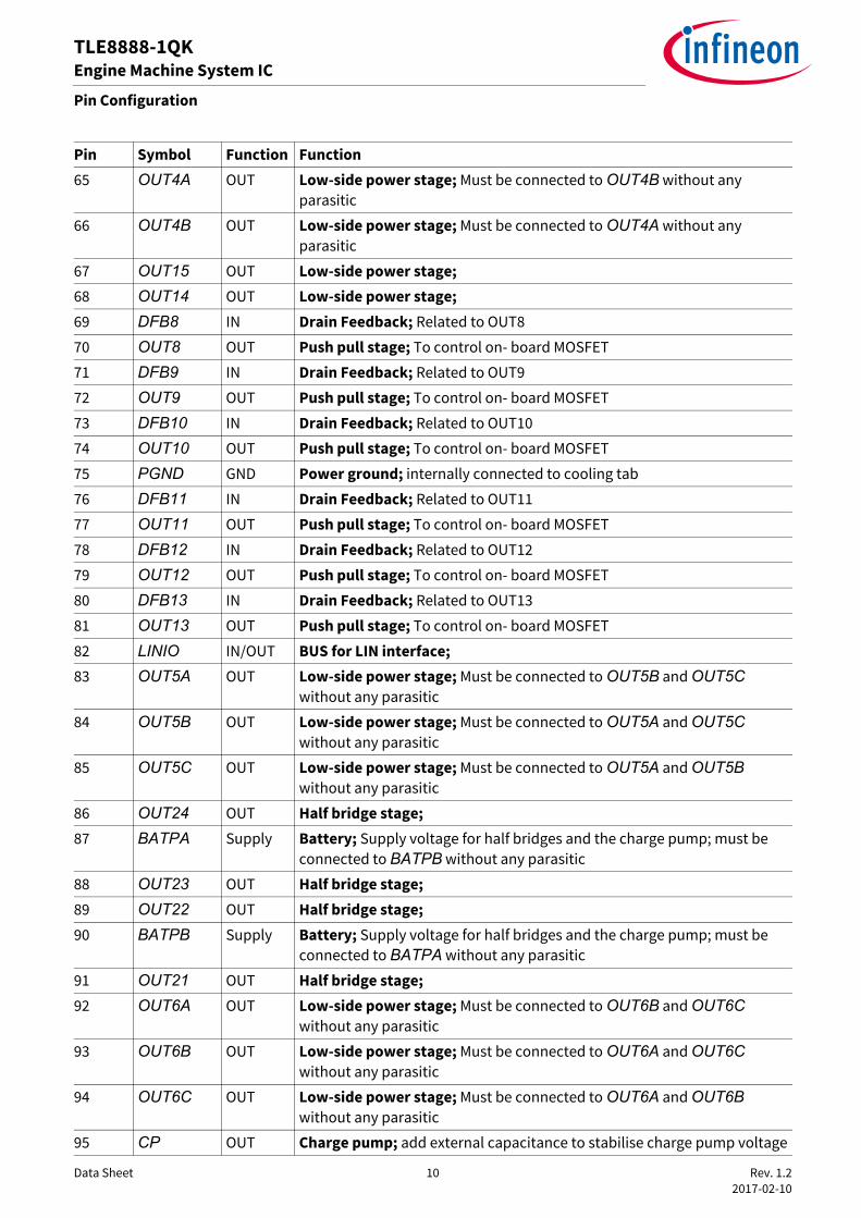
65 OUT4A OUT Low-side power stage; Must be connected to OUT4B without any parasitic
66 OUT4B OUT Low-side power stage; Must be connected to OUT4A without any parasitic
67 OUT15 OUT Low-side power stage;
68 OUT14 OUT Low-side power stage;
69 DFB8 IN Drain Feedback; Related to OUT8
70 OUT8 OUT Push pull stage; To control on- board MOSFET
71 DFB9 IN Drain Feedback; Related to OUT9
72 OUT9 OUT Push pull stage; To control on- board MOSFET
73 DFB10 IN Drain Feedback; Related to OUT10
74 OUT10 OUT Push pull stage; To control on- board MOSFET
75 PGND GND Power ground; internally connected to cooling tab
76 DFB11 IN Drain Feedback; Related to OUT11
77 OUT11 OUT Push pull stage; To control on- board MOSFET
78 DFB12 IN Drain Feedback; Related to OUT12
79 OUT12 OUT Push pull stage; To control on- board MOSFET
80 DFB13 IN Drain Feedback; Related to OUT13
81 OUT13 OUT Push pull stage; To control on- board MOSFET
82 LINIO IN/OUT BUS for LIN interface; 83 OUT5A OUT Low-side power stage; Must be connected to OUT5B and OUT5C
without any parasitic
84 OUT5B OUT Low-side power stage; Must be connected to OUT5A and OUT5C without any parasitic
85 OUT5C OUT Low-side power stage; Must be connected to OUT5A and OUT5B without any parasitic
86 OUT24 OUT Half bridge stage; 87 BATPA Supply Battery; Supply voltage for half bridges and the charge pump; must be
connected to BATPB without any parasitic
88 OUT23 OUT Half bridge stage; 89 OUT22 OUT Half bridge stage; 90 BATPB Supply Battery; Supply voltage for half bridges and the charge pump; must be
connected to BATPA without any parasitic
91 OUT21 OUT Half bridge stage; 92 OUT6A OUT Low-side power stage; Must be connected to OUT6B and OUT6C
without any parasitic
93 OUT6B OUT Low-side power stage; Must be connected to OUT6A and OUT6C without any parasitic
94 OUT6C OUT Low-side power stage; Must be connected to OUT6A and OUT6B without any parasitic
95 CP OUT Charge pump; add external capacitance to stabilise charge pump voltage
Pin Symbol Function Function

Data Sheet 11 Rev. 1.2 2017-02-10
TLE8888-1QKEngine Machine System IC
Pin Configuration
96 IGN1 OUT Push pull stage; To control on- or off- board IGBT
97 IGN2 OUT Push pull stage; To control on- or off- board IGBT
98 IGN3 OUT Push pull stage; To control on- or off- board IGBT
99 IGN4 OUT Push pull stage; To control on- or off- board IGBT
100 AGND GND Signal ground; internally connected to PGND and cooling tab
Cooling tab1)
PGND GND Power ground; internally connected PGND pins
1) Cooling tab is also called exposed pad
Pin Symbol Function Function

Data Sheet 12 Rev. 1.2 2017-02-10
TLE8888-1QKEngine Machine System IC
General Product Characteristics
4 General Product CharacteristicsGeneral definition:VS is the short cut for all battery supplies of the TLE8888-1QK (BAT, BATPA, BATPB, BATSTBY) unlessotherwise specifiedGND is the short cut for all grounds of the TLE8888-1QK (AGND, PGND) unless otherwise specified.
Table 1 Absolute Maximum Ratings1)
Tj = -40°C to +150°C, all voltages with respect to GND, positive current flowing into pin, (unless otherwisespecified)
Parameter Symbol Values Unit Note or Test Condition
NumberMin. Typ. Max.
VoltagesBATPA, BATPB, OUT8…13, DFB8…13
VBATPA,MR, VBATPB,MR, VOUT8…13,MR, VDFB8…13,MR,
-0.3 – 40 V – P_4.1
CP VCP,MR -0.3 – 45 V -0.3 V < VCP -VBATPA < 5 V
P_4.2
OUT1…7, OUT14…20 VOUT1…7,MR, VOUT14…20,MR
-0.3 – 50 V OUTn is switched off, clamping is allowed according Chapter 9.6
P_4.3
V6V VV6V,MR -0.3 – 10 V – P_4.4
VG VVG,MR -0.3 – 12 V VVG - VV6V < 5 V P_4.5
V5V, V5VSTBY, VDDIO, V5VCAN VV5V,MR, VV5STBY,MR, VVDIO,MR, VV5VCAN,MR
-0.3 – 5.5 V – P_4.6
T5V1, T5V2, IGN1…4 VT5V1,MR, VT5V2,MR, VIGN1…4,MR
-1 – 40 V – P_4.7
BAT, BATSTBY, KEY, WK, MR VBAT,MR, VKEY,MR, VWK,MR, VBATSTBY,MR, VMR,MR,
-16 – 40 V – P_4.8

Data Sheet 13 Rev. 1.2 2017-02-10
TLE8888-1QKEngine Machine System IC
General Product Characteristics
IN1…12, SIP, SIN, FCLP, FCLN, CSN, LINTX, CANTX, IGNEN, INJEN, CANWKEN, EOTEN
VIN1…12,MR, VFCLP,MR, VFCLN,MR, VSIP,MR, VSIN,MR, VCSN,MR, VLINTX,MR, VCANTX,MR, VIGNEN,MR, VINJEN,MR, VEOTEN,MR, VCANWKEN,MR
-0.3 – 5.5 V – P_4.9
SDO, RST,VROUT, LINRX, CANRX
VSDO,MR, VRST,MR, VVROUT,MR, VLINRX,MR, VCANRX,MR
-0.3 – VDDIO+0.3
V both conditions must be observed
P_4.31
-0.3 – 5.5 V
MON, KOFFDO VMON,MR, VKOFFDO,MR
-0.3 – V5V+0.3 V both conditions must be observed
P_4.10
-0.3 – 5.5 V
VRIN1 VVRIN1,MR -0.3 – 40 V VRIN2 open P_4.11
VRIN2 VVRIN2_MR -0.3 – 40 V VRIN1 open P_4.12
LINIO, CANH, CANL VLINIO,MR, VCANH,MR, VCANL,MR
-40 – 40 V – P_4.13
OUT21…24 VOUT21…24,MR -0.3 – BATPx+0.3
V – P_4.14
CurrentsDFB8…13 IDFB8…13,MR -5 – 5 mA 2) P_4.15
Common Mode Input Current of VRIN1 and VRIN2
I VRIN,CM,MR -5 – 5 mA I VRIN,CM,MR = I VRIN1 +I VRIN2
2)P_4.16
Common Mode Input Current of VRIN1 and VRIN2, non permanent
I VRIN,CM,MR -15 – 15 mA I VRIN,CM,MR = I VRIN1 +I VRIN2
2), maximum duty cycle 60% and maximum on time of 1 ms, 100 h
P_4.34
Differential Current of VRIN1 and VRIN2
ΔI VRIN,MR -50 – 50 mA ΔI VRIN,MR = (I VRIN1 -I VRIN2)/22)
P_4.17
PGND IPGND,MR -25 – 25 A – P_4.18
IGN1…4 IIGN1…4,MR -50 – – mA 2) P_4.19
Temperatures
Table 1 Absolute Maximum Ratings1) (cont’d)Tj = -40°C to +150°C, all voltages with respect to GND, positive current flowing into pin, (unless otherwisespecified)
Parameter Symbol Values Unit Note or Test Condition
NumberMin. Typ. Max.

Data Sheet 14 Rev. 1.2 2017-02-10
TLE8888-1QKEngine Machine System IC
General Product Characteristics
Notes1. Stresses above the ones listed here may cause permanent damage to the device. Exposure to absolute
maximum rating conditions for extended periods may affect device reliability.2. Integrated protection functions are designed to prevent IC destruction under fault conditions described in the
data sheet. Fault conditions are considered as “outside” normal operating range. Protection functions are not designed for continuous repetitive operation.
Junction Temperature Tj -40 – 150 °C 3) P_4.20
Storage Temperature Tstg -55 – 150 °C – P_4.21
ESD SusceptibilityESD Susceptibility VESDHBM -2 – 2 kV HBM4) P_4.22
ESD Susceptibility BAT, BATPA, BATPB, T5V1, T5V2, BATSTBY, KEY, WK, MR, OUT1…7, OUT14…24, DFB8…13, IGN1…4, CANH, CANL, LINIO, VRIN1, VRIN2 to PGND
VESD,HBM -4 – 4 kV HBM4) P_4.23
ESD Susceptibility VESDCDM -500 – 500 V CDM5) P_4.24
ESD Susceptibility Pin 1, 25, 26, 50, 51, 75, 76, and 100 (corner pins)
VESD1, 25, 26,
50, 51, 75, 76, 100
-750 – 750 V CDM5) P_4.25
1) not subject to production test2) Current has to be limited when maximum voltages are exceeded3) according to qualification4) ESD susceptibility, HBM according to EIA/JESD 22-A114F (1.5k Ω, 100 pF)5) ESD susceptibility, Charged Device Model “CDM” EIA/JESD22-C101 or ESDA STM5.3.1
Table 1 Absolute Maximum Ratings1) (cont’d)Tj = -40°C to +150°C, all voltages with respect to GND, positive current flowing into pin, (unless otherwisespecified)
Parameter Symbol Values Unit Note or Test Condition
NumberMin. Typ. Max.

Data Sheet 15 Rev. 1.2 2017-02-10
TLE8888-1QKEngine Machine System IC
General Product Characteristics
Note: Within the functional range the IC operates as described in the circuit description. The electrical characteristics are specified within the conditions given in the related electrical characteristics table.
Table 2 Functional RangeTj = -40°C to +150°C, all voltages with respect to GND, positive current flowing into pin, (unless otherwisespecified)
Parameter Symbol Values Unit Note or Test Condition
NumberMin. Typ. Max.
Supply Voltage - Reduced Operation
VBAT,ro 4.5 – 6 V reduced operation range, main relay and delayed off power stages are on if enabled, remaining functions not working
P_4.26
Supply Voltage - Low Drop Range
VBAT,ld 6 – 9 V low drop operation range, supply regulators working with supply out of the charge pump, standby supply regulator out of operation range
P_4.27
Supply Voltage - Normal Operation range
VBAT,nop 9 – 28 V normal operation range1)
1) overtemperature due to bad RthJA of the ECU or overload can happen
P_4.28
Supply Voltage - Overvoltage Range
VBAT,ov 28 – 40 V overvoltage, power stages are switched off
P_4.29
Supply Voltage transients2)
2) not subject to production test, specified by design
dVBAT/dt -1 – 1 V/µs – P_4.30
Table 3 Thermal ResistanceParameter Symbol Values Unit Note or
Test ConditionNumber
Min. Typ. Max.Junction to Case1)
1) Not subject to production test, specified by design.
RthJC – 2.4 – K/W – P_4.32
Junction to Ambient RthJA – – – K/W 2)
2) EIA/JESD 52_2, FR4, 80 × 80 × 1.5 mm; 35 × Cu, 5 × Sn; 300 mm2
P_4.33

Data Sheet 16 Rev. 1.2 2017-02-10
TLE8888-1QKEngine Machine System IC
Operation Behavior
5 Operation BehaviorThe TLE8888-1QK has implemented the whole supply of an ECU. Therefore a complex control logic isimplemented to provide several operation states.In this chapter• the ramp up and down behavior and• the status of the TLE8888-1QK during special conditions like 5 V undervoltageis described. For the description of the monitoring watchdog module see Chapter 6.
In Figure 3 the block diagram with all blocks affecting the status of the device and the ECU are shown.Following blocks are influenced during the different operation states and reset functions:• Serial Interface MSC/SPI: with the serial interface the setup of the device is done• Key input detection: start signal from key switch (KL15)• Wake-up input detection: additional start signal e.g. from external CAN with wake-up by bus function• Engine off timer: wake-up signal in comparator mode• Power supply: ECU 5 V supply and 5 V sensor supplies, 5 V standby supply• Voltage monitoring: supervision of all supplies (BAT, V5V, T5V1, T5V2)• Main relay driver: controls external main relay to switch battery voltage to an ECU supply pin (see also
application setups in Chapter 17)• Power stages and half-bridges control block• LIN/K-Line: transmission mode depends on operation state of the ECU• CAN: transmission mode depends on operation state of the ECU, remote wake-up function• Reset outputs MON and RST• Monitoring watchdog module: signature watchdog for safety applications• Operation Mode Control
The operation mode control block consists of:• ramp up and down sequence control logic• the reset control logic and• status output logic.

Data Sheet 17 Rev. 1.2 2017-02-10
TLE8888-1QKEngine Machine System IC
Operation Behavior
Figure 3 Block diagram operation mode control
5.1 Operation StatesIn Figure 4 the state diagram of the whole ramp up and down sequence is shown. There are seven operationstates:• ECU sleep state: KEY and WK input are “low”, no wake-up signals from engine off timer or CAN are active,
main relay is off, the whole ECU inclusive TLE8888-1QK is not supplied, 5 V standby supply is working if pin BATSTBY is supplied, engine off timer and CAN wake-up circuits are active if enabled and supplied.
Power Supply
Main Relay Driver
Power Stages&
Half Bridges
LIN/K-Line
Key Input Detection
Monitoring Watchdog
MSC/SPI
Inpu
t Reg
iste
rO
utpu
t Reg
iste
r
Operation Mode Control
KEY
CSNFCLPFCLN
SIPSIN
SDO
MR
LINIO
MON
RST
BA
TPA
V5V
T5V1
T5V2
Voltage Monitoring
BATS
TBY
V5VS
TBY
Wake Up Input Detection
WK
BAT
BATP
B
Engine Off Timer
Battery Detection
CAN & remote wake up
CANWKENCANLCANH
EOTENOUTxIGNx
CANWKEN

Data Sheet 18 Rev. 1.2 2017-02-10
TLE8888-1QKEngine Machine System IC
Operation Behavior
• Supply ramp up state: KEY input or wake1) are “high” and the supply of the TLE8888-1QK starts working, the voltage of V6V, V5V, T5V1 and T5V2 are ramping up but the voltage levels are below the undervoltage threshold. For wake-up by wake1) the ramp up of the main supply has to be finished before the ramp up timer overflow. The main relay is switched on depending on the voltage level at the pin BAT (see Chapter 7.2)
• Normal operation state: KEY input or wake are “high” and main relay is switched on depending on the voltage level at the pin BAT or the status of bit MR in the status register OpStat0 (see Chapter 7.2), the whole ECU is supplied and the status of the different functions and registers is according Table 5 and Table 6.
• Afterrun state: KEY is “low” but afterrun enable bit is set and therefore the whole ECU is supplied, the status of the different functions and registers is according Table 5 and Table 6 and the microcontroller can execute afterrun routines
• Afterrun reset state: the reset procedure before direct reentry in normal operation is executed if bit AR =1 in the configuration register OpConfig0
• General power-down state: the supplies of the ECU (V5V, T5V1, T5V2) are disabled and the power-down timer is counting, main relay remains in the switching status and the TLE8888-1QK is supplied to ensure the power-down (V5V drops down to 0 V) of the ECU, V5VSTBY is working if BATSTBY is supplied, all functions to external are disabled.
• Wake clear state: this state avoids permanent wake-up in failure cases. The wake clear command is executed (function according setting bit WKCLR in the command register Cmd0). All wake signals which are active after the supply ramp up and the general power-down state are reset.
1) description see Figure 4, Chapter 7.2, Chapter 7.4 and Chapter 12.2.4

Data Sheet 19 Rev. 1.2 2017-02-10
TLE8888-1QKEngine Machine System IC
Operation Behavior
Figure 4 Operation state diagram
ECU Sleep
Supply Ramp Up
Normal Operation*Afterrun*
KEY=1 or wake=1
KEY=0&
wake=0 &AE=0
KEY filtered KEY signalRT_OF ramp up timer overflowAE afterrun enable bitAR afterrun reset configuration bitPDT_OF power down timer overflowPD_OF overflow of minimum one of the three PD counter POR internal power on resetSSOT_OF secure shut off timer overflowV5VUV under voltage of V5V active
0 … function inactive1 … function active
(e.g. V5VUV=1 5V supply is below undervoltage thresholdV5VUV=0 5V supply is above undervoltage threshold)
AfterrunReset*
AR=0 & KEY=1
AR=1 & KEY=1
wake
=0 &
KEY
=0 &
AE=0
* POR=1:active internal power on reset forces transition to ECU sleep (wake=0 & KEY=0) or supply ramp up mode (wake=1 or KEY=1) from all states
PD_O
F=1
or S
SOT_
OF=
1
KEY=0 & wake=0
KEY=0 & wake=1 &
RT_OF=1
Gerneral Power Down*
KEY=0 & AE=1
(PD_OF=1 or SSOT_OF=1) &KEY=0
wake clear*
PDT_OF=1
KEY=1
KEY
=0
(KE
Y=1
orw
ake=
1) &
V5V
UV
=0
wake = WKINT or CANWK or EOTWK
wake = 1: one of the signals WKINT, CANWK, EOTWK is „1"
wake = 0: all signals are „0"

Data Sheet 20 Rev. 1.2 2017-02-10
TLE8888-1QKEngine Machine System IC
Operation Behavior
Description of the transitions:
Table 4 Operation State TransitionsTransition Condition Descriptionfrom all states to ECU sleep state
internal supply voltage < internal por threshold and KEY = 0 and wake1)=02)
internal power on reset is active and reset the whole digital logic, ECU sleep state is entered due to no wake-up signal at KEY or wake
from all states to supply ramp up state
internal supply voltage < internal por threshold and KEY = 1 or wake = 12)
internal power on reset is active and reset the whole digital logic, supply ramp up state is entered due to a wake-up signal at KEY or wake
ECU sleep state to supply ramp up state
KEY > VKEY,th or wake = 1 With a “high” voltage at KEY or wake the wake-up of the TLE8888-1QK starts
Supply ramp up state to ECU sleep state
KEY < VKEY,th and wake = 02)
The external supply ramp up is not finished but the wake-up signals are low
Supply ramp up state to wake clear state
KEY < VKEY,th and wake = 12) and RT_OF = 1
The KEY signal is low and the wake-up signals are active. The ramp up timer has an overflow which indicates a ramp up problem of the external supply (e.g. short to GND). To avoid permanent high current consumption the internal wake signals must be reset to enter the ECU sleep state.
Supply ramp up state to normal operation state
(KEY > VKEY,th or wake = 1) and V5V > Vuv,V5V
2)
normal operation state is entered if the main supply voltage V5V is above the undervoltage threshold, KEY is high or one of the wake-up conditions are active
Normal operation state to afterrun state
KEY < VKEY,th and AE = 12) KEY is “low” and afterrun function is enabled:no changes in the setup of the TLE8888-1QK
Normal operation state to ECU sleep state
AE = 0 and KEY < VKEY,th and wake = 02)
normal shut off
Normal operation state to general power-down state
(PD_OF = 1 or SSOT_OF = 1) and KEY < VKEY,th 2)
KEY is low andwatchdog error shut off with overflow of the power-down counter orsecure shut off due to expired secure shut off timer
Afterrun state to ECU sleep state
AE = 0 and KEY < VKEY,th and wake = 0 2)
normal shut off in afterrun mode with the reset of the afterrun enable bit AE by the microcontroller
Afterrun state to general power-down state
PD_OF = 1orSSOT_OF = 1
watchdog error shut off with overflow of the power-down counter orsecure shut off due to expired secure shut off timer
Afterrun state to normal operation state
KEY > VKEY,th and AR = 02) reentry of normal operation with KEY on during afterrun operation, no reset is performed (AR = 0)
Afterrun state to afterrun reset state
KEY > VKEY,th and AR = 12) reentry of normal operation with KEY on during afterrun operation with reset (AR = 1)
Afterrun reset state to normal operation state
transition to normal operation with the next active internal clock edge after entry to the afterrun reset state

Data Sheet 21 Rev. 1.2 2017-02-10
TLE8888-1QKEngine Machine System IC
Operation Behavior
The two states:• normal operation• afterrunare reflected in the bit OM of the status register OpStat0.The power-down time is defined with the bits PDT of the configuration register OpConfig0.In Figure 5 a sequence with wake-up by KEY and go to sleep with afterrun mode is shown.
Figure 5 Ramp up and down sequence diagram with wake-up by KEY and afterrun mode
5.2 Reset and Operation Modes
General power-down state to wake clear state
PDT_OF = 1 with the power-down timer overflow the reset of the internal wake signals must be performed
Wake clear state to ECU sleep state
KEY < VKEY,th after reset of the internal wake signals and KEY is low the ECU sleep state is entered, no unwanted wake-up due to a failure condition will occur
Wake clear state to supply ramp up state
KEY > VKEY,th after reset of the internal wake signals and KEY is high the supply ramp up state is entered, no unwanted wake-up due to a failure condition at the CAN bus and pin WK will occur
1) wake = WKINT or CANWK or EOTWK (see Chapter 7.2, Chapter 7.4 and Chapter 12.2.4)2) including defined filter times
Table 4 Operation State Transitions (cont’d)Transition Condition Description
wake
RST
t
t
t
ECU Sleep
Supply Ramp Up Normal operationRamp UP/Down
Statemachine Afterrun ECU Sleep
WK
KEY
V5V
VUVV5V
AE
t
tpu,r

Data Sheet 22 Rev. 1.2 2017-02-10
TLE8888-1QKEngine Machine System IC
Operation Behavior
The TLE8888-1QK provides several supervision functions which lead to some dedicated reset states andspecial operation modes of the device and the ECU.There are two bidirectional reset pins MON and RST implemented. For the behavior during reset of the resetpins MON and RST and the other status of the TLE8888-1QK see Table 5 and Table 6.Following reset functions and special states are implemented:• Internal power on reset: the internal power on reset detection circuit monitors the voltage level of the
internal supply. For an internal supply voltage below the internal power on reset threshold the whole digital logic of the TLE8888-1QK is reset which results in the ECU sleep state or supply ramp up state depending on the state of KEY and wake. If the voltage level for operation is high enough the 6 V pre regulator is working. The 5 V supplies are disabled till the internal supply level is over the power on threshold level.
• ECU power on reset: this is the reset at ramp up of the power supplies and the beginning of the operation. The pins RST and MON are pulled to GND to reset the microcontroller and all devices connected to the pin MON. The device is reset to the initial reset status. The reset is released with a voltage at pin V5V higher than the V5V Undervoltage Detection Hysteresis after tpu,r.
• Reset during undervoltage of the 5 V supply V5V: this reset occurs during undervoltage of the 5 V ECU supply. The pins RST and MON are pulled to GND to reset the microcontroller and all devices connected to the pin MON. The delayed switch off function is active regarding the configuration setup. The status of the main relay is according to the status of the wake-up pins KEY and WK and the voltage level of the supply pin BAT.
• State during undervoltage of the 5 V supplies T5V1 and T5V2: with the undervoltage detection of the tracker supplies diagnosis bits are set but there is no effect to the behavior of the device.
• Reset during overvoltage of the 5 V supply V5V: with the overvoltage detection of the 5 V ECU supply all functions of the device which have an effect externally or can lead to overcurrent or overtemperature are disabled (e.g. power stages, LIN/CAN/MSC/SPI communication). The pins RST and MON are low.
• State during overvoltage of the 5 V supplies T5V1 and T5V2: with the detection of overvoltage of the tracker supplies diagnosis bits are set but there is no effect to the behavior of the device.
• Power stages switch off during overvoltage of the battery supply BAT: For voltages at the supply pin BAT higher than the overvoltage threshold the power stages are disabled to avoid too high clamping energy during switch off. Damage of the switches is prevented.
• Watchdog reset: If the reset counter is incremented and the reset is enabled (bit WDREN = 1) the microcontroller is reset with a “low” at the pin RST. The power stages are disabled and the LIN/CAN communication is set to receive only mode.
• Software reset from microcontroller: with the software reset command (command register CmdSR) the software reset is activated. The device is reset to the reset status defined in Table 5 and Table 6. The activation of the software reset triggers an increase of the power-down counter by 1.
• Reset with an external forced “low” at RST: With a detected “low” at the RST pin the TLE8888-1QK is reset to the reset status defined in Table 5 and Table 6.
• Power stages switch off with an external forced “low” at MON: With a detected “low” at the MON pin the power stages are disabled (O1E to O24E, IGN1E to IGN4E are set to “0”). After MON=0 event the power stages must be enabled again.
• State with time out of the MSC communication: With the time out of the MSC communication the power stages are disabled (O1E to O24E, IGN1E to IGN4E are set to “0”). After the next valid received data frame the power stages must be enabled again.
• Afterrun reset: This reset is executed if the bit AR of register OpConfig0 is 1 and the transition from afterrun state to normal operation is triggered (definition see Table 6).

Data Sheet 23 Rev. 1.2 2017-02-10
TLE8888-1QKEngine Machine System IC
Operation Behavior
Table 5 Overview Behavior at Reset and Operation Conditions (part 1)Effect to functions: Conditions
Internal power on reset
ECU power on reset Undervoltage V5V
Undervoltage T5V1, T5V2
Overvoltage V5V1)
Overvoltage T5V1, T5V2
Overvoltage BAT
notes forces state change
only after transition from Supply Ramp Up to Normal Operation state for tpu,r
timing see Chapter 8.7 and Table 7
timing see Chapter 8.7
timing see Chapter 8.7 and Table 7
timing see Chapter 8.7
timing see Chapter 8.7
V5VSTBY, V6V en. en. en. en. en. en. en.
V5V, T5V1, T5V2 dis. en. en. en. en. en. en.
MSC/SPI communication dis. dis. dis. en. dis. en. en.
Main relay en.2) en.2) en.2) en.2) en.2) en.2) en.2)
Low-side switches / Half bridges / Push Pull Driver
off/dis./off off/dis./off off/dis./off no change off/dis./off no change off/dis./off
OUT17 and OUT21 with delayed switch off function
dis. dis. delayed switch off activated
en. delayed switch off activated
en. dis.
LIN/CAN communication dis. rec. only, after release setup acc. bits CAN, LIN, CANWE, LINWE3)
rec. only, after release setup acc. bits CAN, LIN, CANWE, LINWE3)
acc. bits CAN, LIN, CANWE, LINWE
dis., after release setup acc. bits CAN, LIN, CANWE, LINWE
acc. bits CAN, LIN, CANWE, LINWE
acc. bits CAN, LIN, CANWE, LINWE
MON (output function) “low”4) “low” “low” no effect5) “low” no effect5) no effect5)
RST (output function) “low”4) “low” “low” no effect5) “low” no effect5) no effect5)
Watchdog Sequence, Heartbeat Timer6)
reset reset reset no effect reset no effect no effect

Data Sheet 24 Rev. 1.2 2017-02-10
TLE8888-1QKEngine Machine System IC
Operation Behavior
WWD Error Counter, FWD pass counter, Total error counter
reset reset reset no effect reset no effect no effect
PD Counter reset reset reset no effect reset no effect no effect
Reset Counter; SSOT reset reset reset no effect reset no effect no effect
AR; CANWE; LINWE; FWDQUEST
reset reset reset no effect reset no effect no effect
AE; WWDConfig0; WDConfig0; watchdog diagnosis bits
reset reset reset no effect reset no effect no effect
Logic and MSC/SPI register bits7)8)
reset reset reset, diagnosis bit is set
diagnosis bits are set
no effect diagnosis bits are set
diagnosis bit is set
EOTWK, CANWK, WKINT no effect no effect reset no effect no effect no effect no effect1) for voltages greater than the maximum ratings of pin V5V behavior is not guaranteed2) according the definition in Chapter 73) after release of RST (transition from low to high) there is a time delay of tdel,r before configuration is enabled4) active pull down if supply voltage is high enough5) pull up of open drain output is active6) start of watchdog sequence after release of reset7) valid for all register bits which are not described in Table 5 or Table 68) During active delayed switch off mode some register bits related to the power stages are not reset, see Chapter 9.4
Table 5 Overview Behavior at Reset and Operation Conditions (part 1) (cont’d)Effect to functions: Conditions
Internal power on reset
ECU power on reset Undervoltage V5V
Undervoltage T5V1, T5V2
Overvoltage V5V1)
Overvoltage T5V1, T5V2
Overvoltage BAT

Data Sheet 25 Rev. 1.2 2017-02-10
TLE8888-1QKEngine Machine System IC
Operation Behavior
Table 6 Overview Behavior at Reset and Operation Conditions (part 2)Effect to functions: Conditions
Watchdog reset Safe State SW reset from micro-controller
MON switch off (input function)
RST reset (input function)
MSC time out afterrun resetno reset AR=0
reset AR=1
note status during reset pulse top,r
status during reset pulse tint,r
masked by MON output function
masked by RST output function
status till next valid MSC communication
V5VSTBY, V6V en. en. en. en. en. en. en. en.
V5V, T5V1, T5V2 en. en. en. en. en. en. en. en.
MSC/SPI communication
dis. en. en. en. dis. en. en. dis.
Main relay en.1) en. en.1) en.1) en.1) en.1) en.1) en.1)
Low-side switches / Half bridges / Push Pull Driver
off/dis./off off/dis./off off/dis./off3) off/dis./off off/dis./off off/dis./off no change off/dis./off
OUT17 and OUT21 with delayed switch off function
no trigger if termination of delayed switch off function
no trigger if termination of delayed switch off function
dis.3) delayed switch off activated
delayed switch off activated
delayed switch off activated
en. dis.

Data Sheet 26 Rev. 1.2 2017-02-10
TLE8888-1QKEngine Machine System IC
Operation Behavior
LIN/CAN communication
acc. bits CAN, LIN, CANWE, LINWE
acc. bits CAN, LIN, CANWE, LINWE
acc. bits CAN, LIN, CANWE, LINWE
acc. bits CAN, LIN, CANWE, LINWE
rec. only, after release setup acc. bits CAN, LIN, CANWE, LINWE2)
acc. bits CAN, LIN, CANWE, LINWE
acc. bits CAN, LIN, CANWE, LINWE
rec. only, after release setup acc. bits CAN, LIN, CANWE, LINWE2)
MON “low” “low” “low”3) forced from outside
“low” no effect4) no effect4) “low”
RST “low” no effect4) no effect4) no effect4) forced from outside
no effect4) no effect4) “low”
Watchdog Sequence, Heartbeat Timer5)
reset no effect reset no effect reset no effect no effect reset
WWD Error Counter, FWD pass counter, Total error counter
reset no effect reset no effect reset no effect no effect reset
PD Counter no effect no effect increment +1
no effect no effect no effect no effect no effect
Reset Counter; SSOT no effect no effect no effect no effect no effect no effect no effect6) no effect6)
AR; CANWE; LINWE; FWDQUEST
no effect no effect no effect no effect no effect no effect no effect no effect
Table 6 Overview Behavior at Reset and Operation Conditions (part 2) (cont’d)Effect to functions: Conditions
Watchdog reset Safe State SW reset from micro-controller
MON switch off (input function)
RST reset (input function)
MSC time out afterrun resetno reset AR=0
reset AR=1

Data Sheet 27 Rev. 1.2 2017-02-10
TLE8888-1QKEngine Machine System IC
Operation Behavior
AE; WWDConfig0; WDConfig0; watchdog diagnosis bit
reset no effect reset no effect reset no effect no effect reset
Logic and MSC/SPI register bits7)8)
no effect no effect reset no effect reset diagnosis bit is set
no effect reset
EOTWK, CANWK, WKINT
no effect no effect no effect no effect no effect no effect no effect no effect
1) according the definition in Chapter 72) after release of RST (transition from low to high) there is a time delay of tdel,r before configuration is enabled3) status for time top,r4) pull up of open drain output is active5) start of watchdog sequence after release of reset6) SSOT reset due to KEY = 17) valid for all register bits which are not described in Table 5 or Table 68) During active delayed switch off mode some register bits related to the power stages are not reset, see Chapter 9.4
Table 6 Overview Behavior at Reset and Operation Conditions (part 2) (cont’d)Effect to functions: Conditions
Watchdog reset Safe State SW reset from micro-controller
MON switch off (input function)
RST reset (input function)
MSC time out afterrun resetno reset AR=0
reset AR=1

Data Sheet 28 Rev. 1.2 2017-02-10
TLE8888-1QKEngine Machine System IC
Operation Behavior
After a reset with pin RST the configuration of the CAN and LIN bus is delayed by the time tdel,r to avoid thatundefined microcontroller pins are affecting the buses. During this delay time the configuration bits can bechanged by a write access to the register.
Table 7 Reset Time DefinitionReset Function Reset Time at RST Output Related Status Bits in Register
OpStat1internal power on reset all registers are reset
ECU power on reset tpu,r
Undervoltage V5V tpu,r V5VUVROvervoltage V5V tpu,r V5VOVRWatchdog reset top,r WDRESRST reset forced from outside forced from outside RSTRSoftware reset from microcontroller no effect all registers are reset1)
1) internal reset with tint,r active
Afterrun reset AR=”0” no effect
AR=”1” top,r ARES

Data Sheet 29 Rev. 1.2 2017-02-10
TLE8888-1QKEngine Machine System IC
Operation Behavior
5.3 Electrical Characteristics Operation Behavior
Table 8 Electrical Characteristics: Operation BehaviorVS = 13.5 V, VVSV = 5 V, Tj = -40°C to +150°C, all voltages with respect to ground, positive current flowing into pin(unless otherwise specified)
Parameter Symbol Values Unit Note or Test Condition
NumberMin. Typ. Max.
Internal power on reset threshold
Vpor,int,th – – 2.8 V of internal supply voltage
P_5.3.1
Supply voltage range for internal supply
VBATP,int 4.5 – – V only valid if the charge pump has ramped up before voltage drop,both condition must be fulfilled to ensure no internal power on reset
P_5.3.2
VV6V,int 3.5 – – V
Power-Down TimerPower-down time 1 tpd,1 – 100 – ms – P_5.3.3
Power-down time 2 tpd,2 – 200 – ms – P_5.3.4
Power-down time 3 tpd,3 – 300 – ms – P_5.3.5
Power-down time 4 tpd,4 – 400 – ms – P_5.3.6
Power-down time accuracy tpd,a -10 – +10 % – P_5.3.7
Ramp Up timerRamp up time tru 185 – 650 ms – P_5.3.8
MON In- OutputInput low level Vil – – 0.29*V
5VV – P_5.3.10
Input high level Vih 0.7*V5V
– – V – P_5.3.11
Input hysteresis Vihys 0.1 – 1 V – P_5.3.12
Pull up current Iimax -100 – – µA Vin = 0 V,pull up to V5V
P_5.3.13
Input de-glitch time for low and high level detection
ti,d 0.5 – 3.5 µs – P_5.3.14
Output low level operation Vol – – 0.7 V Iout = 2 mA; VV5V = 2.5 V
P_5.3.15
Output current capability Iomax 151) – – mA VMON = 5 V P_5.3.16
RST In- OutputInput low level Vil – – 0.29*V
DDIOV – P_5.3.17

Data Sheet 30 Rev. 1.2 2017-02-10
TLE8888-1QKEngine Machine System IC
Operation Behavior
Input high level Vih 0.7*VDDIO
– – V – P_5.3.18
Input hysteresis Vihys 0.1 – 1 V – P_5.3.19
Pull up current Iimax -100 – – µA Vin = 0 V,pull up to VDDIO
P_5.3.20
Input de-glitch time for low and high level detection
ti,d 0.5 – 3.5 µs – P_5.3.21
Output low level operation Vol – – 0.7 V Iout = 2 mA; VV5V = 2.5 V
P_5.3.22
Output current capability Iomax 151) – – mA VRST = 5 V P_5.3.23
Reset TimesPower up reset time tpu,r 12 16 20 μs – P_5.3.24
Operation reset time top,r 1 2 4 μs – P_5.3.25
Internal reset time tint,r – – 1 µs – P_5.3.26
Delay time after reset tdel,r 6 10 14 µs – P_5.3.271) Application must ensure that current into this pin does not exceed this value.
Table 8 Electrical Characteristics: Operation Behavior (cont’d)VS = 13.5 V, VVSV = 5 V, Tj = -40°C to +150°C, all voltages with respect to ground, positive current flowing into pin(unless otherwise specified)
Parameter Symbol Values Unit Note or Test Condition
NumberMin. Typ. Max.

Data Sheet 31 Rev. 1.2 2017-02-10
TLE8888-1QKEngine Machine System IC
Monitoring Watchdog Module (Signature Watchdog)
6 Monitoring Watchdog Module (Signature Watchdog)
The watchdog function is intended for a temporal and logical monitoring of the microcontroller’s programsequence. In Figure 6 the block diagram of the monitoring module is drawn. The module has an interface tothe MSC/SPI block. The monitoring of the microcontroller is done by the separate check of the timing with thewindow watchdog and the logical operation check by the functional watchdog. Therefore the microcontrollermust send a window watchdog service command for the window watchdog and four response bytes for thefunctional check. The results of the checks affect the corresponding counter (window watchdog error counteror functional watchdog pass counter). Additionally a total error counter module is implemented whichdetects the occurrence of watchdog errors (the timing check or the functional is not passed) and changes thestatus of the total error counter accordingly.For the independent functional watchdog and the total error counter a heartbeat is implemented to define theincrement timing of both functions.
Figure 6 Block diagram of the Monitoring Watchdog Function
Micro Controller
Interface
Window Watchdog Statemachine
Window Watchdog Error Counter
Watchdog Heartbeat
Increment Decrement
Functional Watchdog
Statemachine
Functional Watchdog Pass
Counter
Decrement
RST MON
Response QuestionWindow Watchdog Service Command
Pass WWD Pass FWD
Error Check Statemachine
fail
Total Error Power Down
Counter(Overflow)
OFOF
Power down&
RestartReset Counter
(Overflow)
Reset/Disable Signal Generation
Fail WWD
Total Error Counter
OF
fail
Incr
emen
t
Dec
rem
ent
Increment
Window Watchdog
Power Down Counter
(Overflow)
Functional Watchdog
Power Down Counter
(Overflow)

Data Sheet 32 Rev. 1.2 2017-02-10
TLE8888-1QKEngine Machine System IC
Monitoring Watchdog Module (Signature Watchdog)
The status of the counters (window watchdog error counter, functional watchdog pass counter and total errorcounter) and the corresponding overflow signals are inputs to the watchdog reset, power-down counter andthe secure shut off timer. This information is used to affect the operation status of the TLE8888-1QK and thestatus of the pins MON and RST.The software of the microcontroller has to make sure that the program sequence and any safety critical partsof the microcontroller are self tested by performing related routines according to the received questions.
Table 9 Bit Name Register Type DescriptionGeneralWDRES OpStat1 status reset caused by watchdog (general status bit)
RESC WdStat0 status reset counter value
SSOTS WdStat0 status Secure shut off timer start status
WDHBTPRE WDHBT0 status heartbeat timer pre divider value
WDHBT WDHBT1 status heartbeat timer value
WDHBTP WDConfig0 configuration definition of heartbeat period for functional watchdog and total error counter
CANWE WDConfig1 configuration CAN operation mode during safe state
LINWE WDConfig1 configuration LIN operation mode during safe state
WDREN WDConfig1 configuration watchdog reset enable
FWDQG WDConfig1 configuration Functional watchdog question generation pattern setup
MSCReadWd0 command Multi read command for WdStat0, TECStat, FWDStat0, FWDStat1, WdDiag, WWDStat, WDConfig0 and WWDConfig0
MSCReadWd1 command Multi read command for WDHBT0, WDHBT1, WdStat0 and WdStat1
WDHBTPSyncCmd
command heartbeat period synchronization command
WDHBTS Cmd0 command watchdog heartbeat timer sample command
Window WatchdogWWDEC WWDStat status value of error counter for window watchdog
WWDSCR WdStat0 status Window watchdog service command received status
WWDPDC WdStat0 status power-down counter value of window watchdog
WWDECI WWDConfig1 configuration definition of the increment value of error counter for window watchdog
WWDECD WWDConfig1 configuration definition of the decrement value of error counter for window watchdog
WWDCWT WWDConfig0 configuration closed window time
WWDOWT WWDConfig0 configuration open window time
WWDServiceCmd
command window watchdog service command
WWDSCE WdDiag diagnosis window watchdog service command too early
WWDTO WdDiag diagnosis window watchdog time out

Data Sheet 33 Rev. 1.2 2017-02-10
TLE8888-1QKEngine Machine System IC
Monitoring Watchdog Module (Signature Watchdog)
6.1 Window WatchdogFor the timing check the microcontroller has to send periodically the window watchdog service commandWWDServiceCmd. The window watchdog is triggered correctly if the command is received inside the openwindow of the window watchdog sequence. The check result is used to change the value of the windowwatchdog error counter. If the check is passed the counter will be decremented and for errors it will beincremented. Additionally a write access to configuration register WWDConfig0 causes also anincrementation of the window watchdog error counter. The incrementation of the window watchdog errorcounter (error is occurred) is an input for the total error counter (Chapter 6.3). In Figure 7 the state machineof the window watchdog is shown.The values for incrementation or decrementation can be set in the configuration register WWDConfig1. Thewindow watchdog error counter is a 6 bit counter. The influence of the counter values to the operationbehavior is shown in Table 11 and Table 12.
The window watchdog sequence for the timing check consists of a closed window followed by an openwindow (see Figure 8). A watchdog sequence starts with:• the release of a reset of the monitoring module (see Table 5 and Table 6 in Chapter 5.2)• a window watchdog service command
WWDRES WdDiag diagnosis reset caused by window watchdog
Functional WatchdogFWDQUEST FWDStat1 status question definition
FWDRESPC FWDStat1 status response counter
FWDPC FWDStat0 status pass counter value of functional watchdog
FWDPDC WdStat1 status power-down counter value of functional watchdog
FWDPCI FWDConfig configuration definition of the increment value of pass counter for functional watchdog
FWDPCD FWDConfig configuration definition of the decrement value of pass counter for functional watchdog
FWDKQ WDConfig1 configuration Keep question function set up
FWDRespCmd command response write command
FWDRespSyncCmd
command response write command with heartbeat synchronization at received response byte 0
FWDREA WdDiag diagnosis response error of actual question
FWDREL WdDiag diagnosis response error of last answer
FWDRES WdDiag diagnosis reset caused by functional watchdog
Total Error CounterTEC TECStat status total error counter value
TECPDC WdStat1 status power-down counter value of total error counter part
TECI TECConfig configuration definition of the increment value of total error counter
TECD TECConfig configuration definition of the decrement value of total error counter
TECRES WdDiag diagnosis reset caused by total error counter
Table 9 (cont’d)Bit Name Register Type Description

Data Sheet 34 Rev. 1.2 2017-02-10
TLE8888-1QKEngine Machine System IC
Monitoring Watchdog Module (Signature Watchdog)
• a write to the window time configuration register WWDConfig0• a timer overflow of the watchdog timerIn Figure 8 the two parts of one watchdog sequence are shown. After the power on reset it is running in anendless loop with the defined time for the open and closed window. It is only stopped at active reset signalsor outside normal operating conditions Table 5 and Table 6 in Chapter 5.2.The timing of the window watchdog sequence can be set with a write command to the configuration registerWWDConfig0 or directly with the data bits of the WWDServiceCmd. With a write access to the configurationregister WWDConfig0 the watchdog window sequence is started and the window watchdog error counter isincremented.
The check is passed if the command is received inside the open window. A command send too early or amissing command leads to an error. In the diagnosis register WdDiag the bit WWDSCE signalizes a windowwatchdog service command received too early and the bit WWDTO signalizes a time out (no windowwatchdog service command received before end of open window) of the last sequence. The diagnosisinformation is not cleared with the read out.The bit WWDSCR in the status register WdStat0 signalizes a received window watchdog service command atthe last watchdog sequence. The reset of this bit is done with a readout of the bit or with the window watchdogtime-out.
Figure 7 State Diagram of the Window Watchdog Module
Waiting for WWD
service command
Timing check
Decrement WWD error
counter
Reset
WWD error:Timer expired
ORWrite access to WWDConfig0
Inside open window
WW
D e
rror
:O
utsi
de o
pen
win
dow
Increment WWD error
counter
Start watchdog sequence
WWD service
command

Data Sheet 35 Rev. 1.2 2017-02-10
TLE8888-1QKEngine Machine System IC
Monitoring Watchdog Module (Signature Watchdog)
Figure 8 Watchdog Sequence Timing
6.2 Functional WatchdogFor the functional check the microcontroller has to send with the commands FWDRespCmd (functionalwatchdog response command) or FWDRespSyncCmd (functional watchdog response and synchronisationcommand) the right four response bytes to the actual question defined by the TLE8888-1QK. The responsebytes are checked for correctness.A pass of the check triggers a decrement of the functional watchdog pass counter. A functional watchdog error(FWD error) is not affecting the functional watchdog pass counter but it is used for the total error counter asan input signal (see Chapter 6.3). A FWD error is defined as:• received response byte 0 with FWDRespCmd and minimum one of the response bytes are wrong• received response byte 0 with FWDRespSyncCmd and minimum one of the response bytes are wrong• the watchdog heartbeat timer period synchronisation command WDHBTPSyncCmd is receivedIn the diagnosis register WdDiag the bit FWDREA signalizes an error of the received response bytes to theactual question and the bit FWDREL signalizes an error of the response bytes of the last answer. With a readout the diagnosis bits are not cleared.To detect that the functional check is missing a heartbeat is implemented. With an heartbeat event thefunctional watchdog pass counter is incremented. An heartbeat event occurs:• with expiring of the heartbeat period timer or• with receiving the watchdog heartbeat period synchronisation command WDHBTPSyncCmd (response
counter is also reset) or• with receiving the functional watchdog response and synchronisation command FWDRespSyncCmd if
response byte 0 is receivedThe heartbeat period can be set by a write access to the configuration register WDConfig0 or by the watchdogheartbeat period synchronisation command WDHBTPSyncCmd. If the data is 000 0000B the value of the
WWD Service Command
WWD Service Command
WWD Service Command
tC2 tO2
CSN
tC1 tO1
tC3
WWD Service Command
tC1 tO1
CSN
tC1 tO1
tC2
WWD Service Command
Time out Too early
tO2
Correct Timing of WWDService Command
Wrong Timing of WWDService Command

Data Sheet 36 Rev. 1.2 2017-02-10
TLE8888-1QKEngine Machine System IC
Monitoring Watchdog Module (Signature Watchdog)
heartbeat period is not changed.Behavior of the heartbeat period in case of changing the period time:• WDHBTPSyncCmd: the response counter and the heartbeat timer are reset and a heartbeat event is
triggered, the new value of the period is executed with next period.• write access to the configuration register WDConfig0: the new value of the period is effective after the
write command. If the new value is lower than the actual heartbeat timer value then the heartbeat event is immediately triggered otherwise the actual period length is immediately changed to the new value.
The functional watchdog pass counter is a six bit counter (see status register FWDStat0). The values forincrementation or decrementation can be set in the configuration register FWDConfig. The influence of thecounter values to the operation behavior is shown in Table 11 and Table 12.In Figure 9 the state machine of the functional watchdog is shown. There are two possible principles availableto serve the function watchdog:• unsynchronized heartbeat and use of functional watchdog response command FWDRespCmd and write
access to the configuration register WDConfig0 to change the heartbeat period time or• heartbeat is started with receiving the functional watchdog response and synchronisation command
FWDRespSyncCmd and use of the watchdog heartbeat period synchronisation command WDHBTPSyncCmd for changing the heartbeat period
The commands can be used in all possible combinations without restrictions. Using FWDRespCmd has theadvantage that with fast correct responses the decrement of the functional watchdog pass counter can bespeed up.The bit FWDKQ in the configuration register WDConfig1 is used to enable the keep question function for thefunctional watchdog. If the bit is set in case of a passed functional check the next functional check procedureis done with the same question if minimum one of the bits WWDSCE or WWDTO is set (window watchdogerror).

Data Sheet 37 Rev. 1.2 2017-02-10
TLE8888-1QKEngine Machine System IC
Monitoring Watchdog Module (Signature Watchdog)
Figure 9 Functional Watchdog State diagram
6.2.1 Question and Response DefinitionThe bits FWDQUEST in the watchdog status register FWDStat1 represent the actual valid question.The reset value is 0000B and it will be changed regarding the definition of the state machine for the monitoringmodule (see Figure 7). The expected response is shown in Table 10. The answer of the microcontroller is doneby a write access to the command registers FWDRespCmd or FWDRespSyncCmd.The actual value of the bits FWDRESPC in the watchdog status register FWDStat1 defines the interpretationof the 8 bit content of these commands as RESP3 to RESP0 (definition see FWDRESPC).
Waiting for response 3
Response check
FWD pass counter change1.)
ANDRestart Heartbeat
Timer
Define next question
ResetFW
DRespC
md
OR
FWDRes
pSyn
chCmd
receiv
ed
Correct response
Define start question
Increment FWD pass counter
ANDRestart Heartbeat
Timer
Waiting for response 2
Response check
Waiting for response 1
Response check
Waiting for response 0
Response check
FWD error : Wrong
response2.)
Decrement FWD pass
counter
Correct response
Response check
1.)change value = sum of decrement and increment value2.)wrong response event is also input for the error check statemachine3.) only active if bit FWDKQ=1 , for FWDKQ=0 transition of „No WD error“ is executedWWD error: minimum one of the bits WWDSCE or WWDTO in register WDDiag is high;
FWDRespCmd
OR
FWDRespSynchCmd
received
FWDRespCmd OR
FWDRespSynchCmd received
FWDRespSynchCmd received
FWDRespCmd received
FWD error: Wrong
response 2.)
FWD
erro
r: W
DH
BPSy
nchC
md
rece
ived
No WW
D
error 3.)
No
WW
D
erro
r3.)
WW
D e
rror
3.)
WW
D e
rror3.
)

Data Sheet 38 Rev. 1.2 2017-02-10
TLE8888-1QKEngine Machine System IC
Monitoring Watchdog Module (Signature Watchdog)
The definition of the next question is done with a pseudo random algorithm. With the bit FWDQG in theconfiguration register WDConfig1 the generation algorithm for the questions is defined. There are twosettings:• question pattern length 16: 16 question repeated every 16th watchdog sequence with a minimum
hamming distance of 3• question pattern length 256: every 256 question the order of the 16 questions is repeated, minimum
hamming distance is 1
6.3 Total Error Counter ModuleThe total error module is used to count the errors of the window watchdog and the functional watchdog. InFigure 10 the error check state machine is shown. If a watchdog error of the functional or the windowwatchdog occurs the state machine enters the state “error occurred” and with the next heartbeat event(definition see Chapter 6.2) the total error counter is incremented.The counter is also incremented if a functional watchdog error or at the same time a window watchdog erroroccurs by using the FWDRespSyncCmd. With the WDHBTPSyncCmd always an increment of the total errorcounter is done. A decrement of the total error counter is only possible by using the FWDRespSyncCmd andno errors are occurred.The decrement and increment value of the total error counter can be set with the configuration registerTECConfig. The status of the total error counter is available in the status register TECStat.
Table 10 Questions and related ResponseQUEST[3:0] RESP3 RESP2 RESP1 RESP00 FF 0F F0 00
1 B0 40 BF 4F
2 E9 19 E6 16
3 A6 56 A9 59
4 75 85 7A 8A
5 3A CA 35 C5
6 63 93 6C 9C
7 2C DC 23 D3
8 D2 22 DD 2D
9 9D 6D 92 62
A C4 34 CB 3B
B 8B 7B 84 74
C 58 A8 57 A7
D 17 E7 18 E8
E 4E BE 41 B1
F 01 F1 0E FE

Data Sheet 39 Rev. 1.2 2017-02-10
TLE8888-1QKEngine Machine System IC
Monitoring Watchdog Module (Signature Watchdog)
Figure 10 State diagram of the Error check State machine for the Total Error Counter Module
6.4 Watchdog Reset CounterThe watchdog reset counter is a three bit counter (bits RESC in WdStat0) and is triggered by an overflow ofone of the three counters of the monitoring functions (see Figure 11). The reset counter can only beincremented by 1. Each time the watchdog reset counter changes the value a watchdog reset occursdepending on the status of watchdog reset enable bit WDREN in the configuration register WDConfig1. Thecounter stops counting if WDREN = “0” or at full scale. There are no further resets if full scale is reached. Thebehavior at the different reset conditions is defined in Chapter 5.2 Table 5 and Table 6.
6.5 Power-Down CounterThere are three power-down counters with three bits implemented. The window watchdog power-downcounter (bits WWDPDC in status register WdStat0) is triggered by an overflow of the window watchdog errorcounter, the functional watchdog power-down counter (bits FWDPDC in status register WdStat1) is triggeredby an overflow of the functional watchdog pass counter and the total error power-down counter (bits TECPDCin status register WdStat1) is triggered by an overflow of the total error counter (see Figure 11).If a trigger occurs the dedicated power-down counter is incremented by 1. Additionally all three power-downcounters are incremented by 1 if a software reset occurs. The power-down counters are reset if the ready stateis reached (see Table 11 and Table 12).With an overflow of minimum one of the three power-down counters a power-down of the TLE8888-1QK isperformed if KEY is “low” (see Chapter 5.1). This function can not be disabled. The behavior at the differentreset conditions is defined in Chapter 5.2 Table 5 and Table 6.
6.6 Secure Shut Off TimerThe secure shut off timer (SSOT) is reset with KEY = 1 and the timer starts with an overflow of one of the threecounters of the monitoring functions (see Figure 11) if it is enabled with KEY = 0. If the timer is expired afterthe Secure shut off time a power-down of the TLE8888-1QK is performed (see Chapter 5.1).The behavior atthe different reset conditions is defined in Chapter 5.2 Table 5 and Table 6.
Error occured
Reset
WWD or FWD error
Wait for error
Increment Total error
counter
Hea
rtbea
t ev
ent
Decrement Total error
counter
Error Check Statemachine
FWDRespSyncCmd
received and (functional
check failed or WWD error)
or WDHBTPSyncCmd
FWDR
espS
yncC
md
rece
ived
and
(func
tiona
l che
ck
pass
ed an
d no
WW
D er
ror)

Data Sheet 40 Rev. 1.2 2017-02-10
TLE8888-1QKEngine Machine System IC
Monitoring Watchdog Module (Signature Watchdog)
6.7 Operation State Definition and Reset GenerationThe values of the three counter of the monitoring module are affecting the operation state of the TLE8888-1QK. There are three states defined:• the safe state: this is the reset state. The bits O1E to O24E and IGN1E to IGN4E in the configuration register
OEConfig0 to OEConfig3 are set to “0” to ensure that all actuators are switched off.• ready state: the device can be operated without restrictions.• watchdog reset: a reset is performed according the definition in Table 5 and Table 6.The definition of the three states is shown in Table 11. The states are affecting the status of the pins MON andRST, the power-down counter, the secure shut off timer and the reset counter (definition see Table 12).
Table 11 Definition of Reset, Safe and Ready StateSafe State WWDEC>32D OR FWDPC >32D OR TEC>32D
Ready State WWDEC<33D AND FWDPC<33D AND TEC<33D
Watchdog Reset WWDEC overflow OR FWDPC overflow OR TEC overflow (for all counters >63D)
Table 12 System Reaction to the watchdog statusReady State Safe State Watchdog Reset
RST 1 1 01)
1) occurs for the defined reset time if watchdog reset is enabled
MON 1 0 0
Power stages no influence of normal operation
disabled disabled
O1E to O24E, IGN1E to IGN4E
X 0 0
WWD error counterFWD pass counterTotal error counter
no effect no effect reset1)
Reset counter no effect no effect increment by 1
Window watchdog power-down counterTotal error power-down counterFunctional watchdog power-down
reset no effect increment by 1 regarding the overflow source
Secure shut off timer no effect no effect start of timer with the first overflow if KEY = 0

Data Sheet 41 Rev. 1.2 2017-02-10
TLE8888-1QKEngine Machine System IC
Monitoring Watchdog Module (Signature Watchdog)
Figure 11 Block diagram of the Reset Generation
Behavior of the WWD error counter, the FWD pass counters and the total error counter in case of over and underflow:The counters are designed to keep the same value:• at incrementation if the new counter value is higher than the full scale value of the counter and• at decrementation if the new counter value is lower than zero.In Figure 12 an example is shown.
63
32
0
Ready
Safe
Overflow
33
Reset Value=48
63
32
0
Ready
Safe
Overflow
33
Reset Value=48
Window WatchdogError Counter
Functional WatchdogPass Counter
Reset Generation
Total Error Power Down Counter
Power Down
Reset Counter RST
MON
Total Error Counter
63
32
0
Ready
Safe
Overflow
33
Reset Value=48
counter reset
Functional Watchdog Power Down Counter
Window Watchdog Power Down Counter

Data Sheet 42 Rev. 1.2 2017-02-10
TLE8888-1QKEngine Machine System IC
Monitoring Watchdog Module (Signature Watchdog)
Figure 12 Example of WWD error counter behavior with decrement and increment value of 14d
6.8 Synchronisation of Window Watchdog Sequence and HeartbeatIn Figure 13 the relation between the heartbeat clock generation, the total error counter and the windowwatchdog sequence generation is shown. The window watchdog sequence generation and the heartbeatperiod generation have the same clock base with the accuracy of tw,a.The value of the pre-divider and the heartbeat timer can be read out with the status registers WDHBT0 andWDHBT1. This can be used to measure the actual internal clock frequency. Therefore the value of the pre-divider and the heartbeat period counter must be sampled by sending a Cmd0 command with an activatedWDHBTS bit. With this command the value of the two registers are stored in the related status registers andthe readout can be done.With two sampled values the microcontroller can correct the time information by the value of the actualfrequency of the TLE8888-1QK. With such a correction of the microcontroller timing check it is possible to usesmaller open window times to improve the performance of the timing check. Additional it is possible to usethis information for synchronization purpose for the check of the monitoring function of the TLE8888-1QKinside the microcontroller.
Restart of window watchdog period
Safe State
Ready State
WWD Error Counter
Full scale 63d
1 2 3 4 5 6 7 8
Reset Value 48d
40d
32d
24d
16d
0d
8d
56d
Overflow
Underflow
62d
34d
20d
6d
Decrement Value = Increment Value = 14dWDREN=0

Data Sheet 43 Rev. 1.2 2017-02-10
TLE8888-1QKEngine Machine System IC
Monitoring Watchdog Module (Signature Watchdog)
Figure 13 Clock Generation for the Watchdog Module
Window Watchdog
Pre Divider
Functional Watchdog
Pass Counter
Increment
Decrement
fclk fclk/16
fclk used for watchdog sequence
Heartbeat for Functional Watchdog
Functional Watchdog Setting
7 bit counter
Error Check Statemachine

Data Sheet 44 Rev. 1.2 2017-02-10
TLE8888-1QKEngine Machine System IC
Monitoring Watchdog Module (Signature Watchdog)
6.9 Electrical Characteristics Monitoring Watchdog Module
Table 13 Electrical Characteristics: Monitoring Watchdog ModuleVS = 13.5 V, VVSV = 5 V, Tj = -40°C to +150°C, all voltages with respect to ground, positive current flowing into pin(unless otherwise specified)
Parameter Symbol Values Unit Note or Test Condition
NumberMin. Typ. Max.
Window watchdog closed window time
tWWD,ct 1.6 – 100.8 ms 63 values P_6.8.1
Window watchdog closed window time step
tWWD,ct – 1.6 – ms – P_6.8.2
Window watchdog open window time 1
tWWD,ot1 – 3.2 – ms P_6.9.1
Window watchdog open window time 2
tWWD,ot2 – 6.4 – ms P_6.9.2
Window watchdog open window time 3
tWWD,ot3 – 9.6 – ms P_6.9.3
Window watchdog open window time 4
tWWD,ot4 – 12.8 – ms – P_6.8.3
Clock frequency accuracy for window watchdog sequence and heartbeat
tw,a -5 – +5 % – P_6.8.4
Heartbeat time period tHBT,pt 1.6 – 203.2 ms 127 values P_6.9.4
Secure shut off time tSSOT 18 20 22 min – P_6.8.5

Data Sheet 45 Rev. 1.2 2017-02-10
TLE8888-1QKEngine Machine System IC
Wake-Up Detection and Main Relay Driver
7 Wake-Up Detection and Main Relay DriverThe TLE8888-1QK integrates a complex wake-up functionality with two wake-up pins (KEY and WK), engineoff timer, CAN wake-up and the main relay driver. There are several possibilities to initiate the start up of thedevice:• a positive voltage at the pin KEY or at the pin WK• a dominant pulse at the CAN inputs CANH and CANL for the wake-up time (description see Chapter 12)• after expiration of the defined time of the engine off timer in comparator modeWith minimum one valid wake-up signal the pre regulator and the main supply start the ramping up due tovoltage at the battery supply pin BAT and the drain of the external MOSFET of the pre regulator. The switchon of the main relay depends on the wake-up signal and the voltage level at the pin BAT. For a wake signalfrom the pin KEY the main relay is always switched on. For the other cases the main relay is only switched onif the voltage of the pin BAT is below the detection threshold.With the bit WKCLR in the command register Cmd0 the internal status of the detection at pin WK, engine offtimer and CAN wake-up are reset (description see Chapter 7.2, Chapter 7.4 and Chapter 12.2.4). The supplyfor the engine off timer and the CAN wake receiver is V5VSTBY.
Figure 14 Block Diagram of the Key Detection, Wake-up Detection and Main Relay Driver
Main Relay DriverKey Detection
Wake Up Pin Detection
Internal Supply
Key On
Wake Up MR
MRKEY
WK
BAT
Wake Up Supply
Supply
Engine Off Timer
EOTEN
Digital Block
Battery Detection
Logic
WK_High
EOTWK
BA
T_H
igh
CAN Wake Receiver
CANWKEN
CA
NW
K
Digital block
KOFFDO
Main Relay Supply
Standby Supply
BAT STBYV5VSTBY
MSC/SPI InterfaceSDO
SIN WKCLR
MR On/Off
connection to VDDIO or V5V

Data Sheet 46 Rev. 1.2 2017-02-10
TLE8888-1QKEngine Machine System IC
Wake-Up Detection and Main Relay Driver
7.1 Wake-up Detection by Pin KEY and Key Off DelayThe input pin KEY is implemented to detect the status of the key switch in the car. With a high signal the startup of the TLE8888-1QK is initiated. During start up the implemented circuitry provides also the supply forswitching the main relay. A deglitch filter is implemented to be robust against disturbances (see Figure 16).After ramp up the supply of the main relay is provided by the internal supply. To provide a direct access fromthe KEY signal to actuators a key off delay function is implemented.
Figure 15 Block Diagram of the Key Detection
In Figure 16 the effect of the filter time is shown. The status of the pin KEY including the filter time is reflectedin bit KEY in the status register OpStat0.
Table 14 Switching Behavior of Main Relay at Start Up (Transition ECU Sleep to Supply Ramp Up Mode)
KEY = 0, WK = EOTWK = CANWK= 0 - MR is switched off Supply is off
KEY = 1, WK = EOTWK = CANWK= X - MR is switched on Supply is switched onKEY = 0, WK or EOTWK or CANWK = 1 BAT < VBAT,th MR is switched on
KEY = 0, WK or EOTWK or CANWK= 1 BAT > VBAT,th MR is switched off
Key Detection Key On
KOFFDO
KEY
Supply
Main Relay
Key Off Delay
Register
Internal Supply
connection to VDDIO or V5V

Data Sheet 47 Rev. 1.2 2017-02-10
TLE8888-1QKEngine Machine System IC
Wake-Up Detection and Main Relay Driver
Figure 16 Function of Key detection filter time
The key off delay function provides the KEY signal at the open drain output KOFFDO. The positive edge isdelayed by the Key Detection Filter Time and the negative edge by the Key Off Delay Time 1 to Key Off DelayTime 4 (according setup of the bits KOD in register OpConfig0) if the supply is available.
Figure 17 Timing Diagram of the Key Off Delay
7.2 Wake-up Detection by Pin WKThe pin WK is used e.g. for an external CAN device with wake-up function on the ECU. With a high signal thestart up of the TLE8888-1QK is initiated. During ramp up the supply for the main relay circuit is provided by theactive wake-up pin WK. After ramp up the supply of the main relay circuit is provided by the internal supply.In Figure 18 the block diagram of the wake-up detection by pin WK is shown.
KEY
t
Wake Up by Signal at Pin KEY ; WK = EOTWK = CANWK = 0; AE=0
ECU Sleep Supply Ramp Up Normal operationRamp UP/Down
Statemachine ECU Sleep
tKEY,f tKEY,f
V5V
KOFFDO t
ttKEY,f tKoff,d
KEY
VDDIO

Data Sheet 48 Rev. 1.2 2017-02-10
TLE8888-1QKEngine Machine System IC
Wake-Up Detection and Main Relay Driver
Figure 18 Block Diagram of the Wake-up Detection
For wake-up by pin WK special functions are implemented. • main relay is switched on depending on the voltage level at pin BAT (see Table 14)• power-down procedure in case of a permanent WK = “1” and a blocked micro-controller (see description
in Chapter 5.1 Operation States) • wake clear bit WKCLR in the command register Cmd0 to clear the internal wake-up signal in case of
permanent WK = “1” signal• deglitch filter of tWK,f for positive and negative edge at pin WKIn Figure 19 the effect of the filter time is shown. The status of the pin WK including the filter time is reflectedin bit WK in the status register OpStat0.
Figure 19 Function of WK detection filter time
To realize the power-down procedure an internal wake-up signal WKINT is used (status see bit WKINT in thestatus register OpStat0). In Figure 20 the state diagram of the internal wake signal generation is shown. With
Wake Up Pin Detection
Supply
Wake Up MR
WK BAT
Wake Up SupplyFilterWake Up Pin Detection
BAT Detection
WKINT
WKCLR
WK
Wake Statemachine
WK
t
Bit WK in OpStat0
tWKINT
tWK,f tWK,ft

Data Sheet 49 Rev. 1.2 2017-02-10
TLE8888-1QKEngine Machine System IC
Wake-Up Detection and Main Relay Driver
a positive edge at pin WK the internal signal WKINT is set to “1” and a wake-up is triggered. With a wake-upclear command (set bit WKCLR to “1” in command register Cmd0) WKINT is reset (see Figure 22). The nextwake-up by pin WK is only detected with a positive edge at pin WK. A permanent high level at pin WK doesn’tlead to permanent wake-up situation. Details of the operation behavior see Chapter 5.1 Operation States.
Figure 20 State Diagram of the Wake State Machine for Internal Wake Signal
At the beginning of the functional diagram of Figure 21 a normal wake-up sequence with a wake signal of thepin WK is shown. In the second part of the diagram the signal of pin WK stick at high (e.g. short to battery) andthe microcontroller must send a wake clear command (bit WKCLR = 1 in command register Cmd0) for enteringthe ECU sleep mode. With a low at pin WK the wake state machine is set to the state “WK inactive” and a wake-up by pin WK is enabled.
WK activeWKINT=1
WK inactiveWKINT=0
WK disabled
WKINT=0
WK
< V W
K,th
1)
WK > VWK,th1)
WK > V
WK,th 1)&
WKCLR=1
WK < VWK,th & WKCLR=1
1) transition after Wake Up detection Filter Time

Data Sheet 50 Rev. 1.2 2017-02-10
TLE8888-1QKEngine Machine System IC
Wake-Up Detection and Main Relay Driver
Figure 21 Functional Diagram for Internal Wake Signal
Figure 22 Functional Diagram of Detection of Two Internal Wake Signals
7.3 Main Relay DriverThe main relay driver is designed to switch on the main relay of engine management applications. It integratesa reverse protected low-side switch with active clamping freewheeling. The output is protected againstoverload with an overtemperature detection and an overcurrent protection circuit. At low battery voltage(V5V main supply is below undervoltage detection threshold e.g. during cranking) the main relay stays on.The on resistance is related to the supply voltage at pin BAT and is defined down to 4.5 V.The main relay is automatically switched on with a wake-up signal according to Table 14. The main relay isnormally switched off automatically according the power-down procedure defined in Chapter 5.With write access to the command bit MRON of the command register Cmd0 the main relay can be switched
WK
CSNMSC Communication
t
t
Internal Wake Up signal WKINT1)
t
Set WKCLR=“1“
WK inactive
WK active
WK inactive WK activeStatus Wake
Statemachine1) WK disabled WK inactive
WK active
ECU Sleep
ECU Sleep ECU Sleep
Wake Up by Signal at Pin WK ; KEY = EOTWK = CANWK = 0; AE=0
1) Wake Up Detection Filter Time is not shown in the diagram
Set WKCLR=“1“
WK
t
WKINT1)
t
wake
tSet
WKCLR=“1“
Wake Up by Signal at Pin WK ; KEY = EOTWK = CANWK = 0, AE=1
1)Wake Up detection Filter Time is not shown in the diagram

Data Sheet 51 Rev. 1.2 2017-02-10
TLE8888-1QKEngine Machine System IC
Wake-Up Detection and Main Relay Driver
additionally by MSC/SPI control according to the status of KEY, WK, EOTWK and CANWK (see Table 15). Thestatus of the main relay is available in the status register OpStat0 bit MR.
The main relay driver is protected against overcurrent and overtemperature. In the case of overcurrent and/orovertemperature the output is switched off and is switched on again after release of the failure condition. Thisleads to a repetitive switching. A minimum off time tMR,off is implemented to ensure no destruction due torepetitive switching.
7.4 Engine Off TimerThe engine off timer is integrated to measure the time in ECU sleep mode. Additionally the comparator modeis implemented to wake-up the TLE8888-1QK after a defined time. It is internally supplied out of the standbysupply pin V5VSTBY. With the pin EOTEN the function is enabled with a connection to V5VSTBY anddisabled with a connection to AGND. It consists of an oscillator optimized for low current operation, a counterand a comparator. The counter counts up to 36 hours and if the counter value reaches the comparatorthreshold an internal wake-up signal is generated. The activation of the comparator mode is done with adefinition of a comparator threshold greater than 0000H in configuration registers EOTConfig0 andEOTConfig1. There are two operation modes implemented:• Counter Mode: only counter is working, no wake-up with comparator threshold• Comparator Mode: counter operation like counter mode, additional wake-up with comparator thresholdIn comparator mode the internal EOTWK flag is set if the counter is equal to compare value in theconfiguration registers EOTConfig0 and EOTConfig1. The reset of the EOTWK flag is done with the bit WKCLRin the command register Cmd0 if the counter value is not equal to the compare value.
Figure 23 Block Diagram Engine Off Timer
The start of the counter can be configured with the bit EOTCONF in the configuration register OpConfig0 to• start by KEY signal (reset value) and• start by MSC command
Table 15 Effect of MSC/SPI Write Command Bit MRONKEY = 0, WK = EOTWK = CANWK = X MR is switched according to write commandKEY = 1, WK = EOTWK = CANWK = X MR is always switched on
Oscillator Counter Comparator
V5VSTBY
KEY KEY Detection Digital Block
Sta
rt
EOTWKEOTEN
MSC/SPI Interface SDO
SIN
EOTWK flag
WKCLR
EOTRES

Data Sheet 52 Rev. 1.2 2017-02-10
TLE8888-1QKEngine Machine System IC
Wake-Up Detection and Main Relay Driver
With the falling edge of the KEY signal or with the execution of the MSC command the counter is reset andstarts counting (see Figure 24). The start command is performed with setting the bit EOTS to “1” in thecommand register Cmd0.The status bit EOTRES (register OpStat1) is implemented to highlight that a standby reset has happened. Withthe start of the counter this bit is reset. Therefore the status of this bit must be readout before the start of theengine off timer.The 24 bits of the counter are available in the status register EOTStat0, EOTStat1 and EOTStat2. For easieraccess to the engine off timer status the multiple read command MSCReadDiag0EOT is implemented.After wake-up the counter doesn’t stop counting. A readout of the counter value doesn’t stop counting. Withthis behavior it is possible to measure the counting time with the microcontroller (see Figure 25).With a read out of two counter values in a defined time a correction factor can be calculated (difference ofcounter values divided by the time between the two read outs). With this measurement of the correctionfactor only the variation caused by the temperature of the timer are effective. The absolute variations arecorrected by the correction factor. There are no restrictions for the measurement time but due to theresolution of the counter a minimum measurement time ∆t of 1 s is recommended.After power-up of the engine off timer circuit with a supply ramp up at pin V5VSTBY the counter value andthe comparator threshold are reset to the reset value. Additionally the bit EOTRES in the status registerOpStat1 is set to “1”.Any other resets like ECU power on reset have no impact to the engine off timer counter. The compareconfiguration register EOTConfig0 and EOTConfig1 are cleared with an ECU power on reset.The counter stops counting at full scale. If a standby supply reset occurs the counter stops counting and isreset to “0”.
Figure 24 Function Diagram Engine Off Timer Counter Mode
KEY
EOT Counter Value
full scale
CSNMSC Communication
readout counter value
set configuration
„start by command“
command start
counter
Configuration „Start by Key Signal“ Configuration „Start by Command“
t
t
t
ECU Sleep ECU Sleep ECU Sleep
WK = EOTWK = CANWK = 0; AE=0

Data Sheet 53 Rev. 1.2 2017-02-10
TLE8888-1QKEngine Machine System IC
Wake-Up Detection and Main Relay Driver
Figure 25 Function Diagram Engine Off Timer Correction Factor Measurement
In comparator mode there is no difference in the behavior of the counter as described above. Additionally acomparator threshold different to 0000H for wake-up is defined in the configuration register EOTConfig0 andEOTConfig1. The comparator mode is enabled with a threshold value different to 0000H. If the counter valueis equal to the comparator threshold the internal wake-up signal EOTWK (status see bit EOTWK in the statusregister OpStat0) of the TLE8888-1QK is active (see Figure 26).With a wake-up clear command (set bit WKCLR to “1” in command register Cmd0) the internal EOTWK signalis reset.
Table 16 Counter DefinitionEOTC[23:0]000000H reset value
000001H to FFFFFFH 1/128 s to 131071 s = 36 h + 24 min + 31 s time resolution 1/128 s
Table 17 Comparator Threshold DefinitionEOTTH[15:0]0000H reset value comparator mode disabled
0001H to FFFFH 2 s to 131070 s = 36 h + 24 min + 30 s comparator mode enabled, time resolution 2 s
KEY
EOT Counter Value
full scale
CSNMSC Communication
readout counter value 1
t
t
t
ECU Sleep
WK = EOTWK = CANWK = 0; AE=0
readout counter value 2
∆t
Correction Factor =value 2 – value 1
∆t

Data Sheet 54 Rev. 1.2 2017-02-10
TLE8888-1QKEngine Machine System IC
Wake-Up Detection and Main Relay Driver
Figure 26 Function Diagram Engine Off Timer Comparator Mode
KEY
EOT Counter Value
full scale
CSNMSC Communication
readout counter value
command start
counter
t
t
t
EOTWK
t
comparator threshold
setWKCLR = “1"
readout counter value
ECU Sleep
ECU Sleep
ECU Sleep

Data Sheet 55 Rev. 1.2 2017-02-10
TLE8888-1QKEngine Machine System IC
Wake-Up Detection and Main Relay Driver
7.5 Electrical Characteristics Key Detection, Wake-up Detection and Main Relay Driver
Table 18 Electrical Characteristics Key DetectionVS = 13.5 V, VVSV = 5 V, Tj = -40°C to +150°C, all voltages with respect to GND, positive current flowing into pin,(unless otherwise specified)
Parameter Symbol Values Unit Note or Test Condition
NumberMin. Typ. Max.
Key On Detection Threshold VKEY,th 3.6 – 4.5 V rising edge P_7.5.1
Key On Detection Hysteresis VKEY,h 140 250 400 mV – P_7.5.2
Input Current during wake-up IKEY – – 0.55 mA VKEY = 5 V1)
1) not subject to production test, specified for design
P_7.5.3
Input Current after wake-up IKEY – – 0.7 mA VKEY = VBAT = 4.5 V
P_7.5.31
Key Detection Filter Time tKEY,f 7.5 16 24 ms VKEY = 5 V P_7.5.4
Key Off Delay Time 1 tKEYoff,d,1 100 – 200 ms – P_7.5.5
Key Off Delay Time 2 tKEYoff,d,2 200 – 400 ms – P_7.5.6
Key Off Delay Time 3 tKEYoff,d,3 400 – 800 ms – P_7.5.7
Key Off Delay Time 4 tKEYoff,d,4 800 – 1600 ms – P_7.5.8
Output KOFFDOOutput Current Capability IKOFFDO 152)
2) Application must ensure that current into this pin does not exceed this value.
– – mA VKOFFDO = 5 V P_7.5.9
KOFFDO Output Low Level VKOFFDO,low – – 0.4 V IKOFFDO < 1 mA P_7.5.30
Table 19 Electrical Characteristics Wake-up DetectionVS = 13.5 V, VVSV = 5 V, Tj = -40°C to +150°C, all voltages with respect to GND, positive current flowing into pin,(unless otherwise specified)
Parameter Symbol Values Unit Note or Test Condition
NumberMin. Typ. Max.
Wake-up Detection Threshold VWK,th 3.6 – 4.5 V rising edge P_7.5.10
Wake-up Detection Hysteresis VWK,h 140 250 400 mV – P_7.5.11
Input Current during Wake-up IWK – – 0.55 mA VWK = 5 V1)
1) not subject to production test, specified by design
P_7.5.12
Wake-up Detection Filter Time tWK,f 1 2 3.5 ms VWK = 5 V P_7.5.13
Battery Detection Threshold VBat,th 3.5 – 5 V VWK = 5 V P_7.5.14

Data Sheet 56 Rev. 1.2 2017-02-10
TLE8888-1QKEngine Machine System IC
Wake-Up Detection and Main Relay Driver
Table 20 Electrical Characteristics Main Relay DriverVS = 13.5 V, VVSV = 5 V, Tj = -40°C to +150°C, all voltages with respect to GND, positive current flowing into pin,(unless otherwise specified)
Parameter Symbol Values Unit Note or Test Condition
NumberMin. Typ. Max.
MR Operation Current IMR – – 0.8 A – P_7.5.15
MR Overcurrent Limitation IMR,oc 0.8 – 1.5 A – P_7.5.16
MR On Voltage VMR – – 1.35 V IMR = 0.3 A P_7.5.17
MR switch off time in failure case
tMR,off 16 27 – ms in case of overcurrent and/or over-temperature
P_7.5.32
MR On Voltage at Low Battery Voltage, low temperature
VMR,l,LT – – 1.1 V IMR = 0.1 A, VBAT = 4.5 V (decreasing)TJ < 25°C
P_7.5.18
MR On Voltage at Low Battery Voltage, high temperature
VMR,l,HT – – 1.05 V IMR = 0.1 A, VBAT = 4.5 V (decreasing)TJ > 25°C
P_7.5.19
MR Clamping Voltage VMR,cl 40 – 60 V IMR = 0.2 A P_7.5.20
MR Clamping Energy1)
1) not subject to production test
EMR,cl – – 6.5 mJ IMR < 0.3 A, Tj = 150°C, 40*106 cycles
P_7.5.21
MR leakage current in off mode, positive voltage
IMR.leak,pos – – 5 µA VMR = 13.5 V,VKEY = 0 V and VWK = 0 V
P_7.5.22
MR leakage current in off mode, negative voltage
IMR.leak,neg -100 – – µA VMR = -13.5 V,VKEY = 0 V and VWK = 0 V
P_7.5.23
Table 21 Electrical Characteristics Engine Off TimerVS = 13.5 V, VVSV = 5 V, Tj = -40°C to +150°C, all voltages with respect to GND, positive current flowing into pin,(unless otherwise specified)
Parameter Symbol Values Unit Note or Test Condition
NumberMin. Typ. Max.
Oscillator Accuracy Δfosc,a -30 – +30 % VV5VSTBY = 5 V P_7.5.24
Oscillator Frequency Variation over Temperature
Δfosc,T -5 – +5 % VV5VSTBY = 5 V,Tj = -40°C to 85°C, one single device
P_7.5.25
Counter Resolution CEOT,r – 1/128 – s – P_7.5.26

Data Sheet 57 Rev. 1.2 2017-02-10
TLE8888-1QKEngine Machine System IC
Wake-Up Detection and Main Relay Driver
Counter Full Scale CEOT,fs – – 24 bit – P_7.5.27
– 131071 – s –
Additional current consumption at pin BATSTBY for enabled engine off timer function
IEOTSUP – – 10 µA VV5VSTBY = 5 V and no wake-up
P_7.5.28
Additional current consumption at pin BATSTBY for enabled engine off timer function and wake-up1)
IEOTSUP,w – – 450 µA VV5VSTBY = 5 V and wake-up
P_7.5.29
1) not subject to production test, specified by design
Table 21 Electrical Characteristics Engine Off Timer (cont’d)VS = 13.5 V, VVSV = 5 V, Tj = -40°C to +150°C, all voltages with respect to GND, positive current flowing into pin,(unless otherwise specified)
Parameter Symbol Values Unit Note or Test Condition
NumberMin. Typ. Max.

Data Sheet 58 Rev. 1.2 2017-02-10
TLE8888-1QKEngine Machine System IC
Power Supply
8 Power SupplyThe power supply unit generates the internal supply (including supply for CAN and pre-drivers, voltagereference and current biasing), the main supply voltage for the ECU (V5V) and sensor supplies for off- boardsensors (T5V1 and T5V2). All supplies start working by the wake-up signal generated by the key and wake-updetection (see Chapter 7.2 for details).A linear pre-regulator with an external logic level power MOSFET is implemented to keep the powerdissipation of the TLE8888-1QK low. The precise voltage supplies for the ECU and the sensor supplies areintegrated inclusive the power transistor. All supplies with low drop functionality (main supply V5V, pre-regulator, sensor supplies T5V1/T5V2) are using an integrated charge pump to provide low drop behavior atlow battery voltages.
Figure 27 Block diagram of the power supply
8.1 Pre-RegulatorThe pre-regulator uses an external logic level power MOSFET and regulates the voltage at pin V6V. Thevoltage at the pin is also the input voltage for the main supply of the ECU (V5V), the sensor supplies (T5V1,T5V2) and the internal supply. The circuit is designed for low drop operation.It's not allowed to load the external MOSFET with anything else than V6V. The function of the pre-regulator isguaranteed with the MOSFET IPD30N06S2L-23 of Infineon.
V5V
T5V1
VG
V6V
T5V2
+
-
+
-
+
-
Linear Preregulator
Linear Regulator
Tracker
Ref
Ref
VV5V
CPBATSTBY
Standby RegulatorV5VSTBY Chargepump
VDDIO
Digital Outputs to
Micro Controller
To Micro Controller
Half Bridges
BATPA BATPB
Key and Wake Up Detection
BAT

Data Sheet 59 Rev. 1.2 2017-02-10
TLE8888-1QKEngine Machine System IC
Power Supply
8.2 5 V Main Supply The 5 V main supply is designed to supply the ECU including microcontroller and e.g. other power chips. Outof V6V a high accurate voltage is provided at the pin V5V. The pin and the circuit is protected against overloadand short circuit. For stabilization and ripple reduction an external buffer capacitor is required. For low dropoperation of the regulator the pins BATPA and BATPB must be supplied.
8.3 Sensor SupplyThere are two sensor supplies integrated providing an output voltage based on V5V as reference. Out of V6Va high accurate voltage is provided at the pins T5V1 and T5V2. The pins and the circuits are protected againstoverload, short circuit and reverse supply back to V6V. For stabilization and ripple reduction external buffercapacitors are required. For low drop operation of the regulator the pins BATPA and BATPB must besupplied.
8.4 IO SupplyThe TLE8888-1QK provides an IO supply pin VDDIO for 3.3 V and 5 V microcontroller interfaces. This pin isused for the supply of the output driver and defines the output level of all logical interface pins.
8.5 Standby SupplyThe TLE8888-1QK integrates a standby supply which is supplied by the pin BATSTBY and provides a 5 Voutput supply at pin V5VSTBY. It is not allowed to connect this pin to any other supply.
8.6 Charge PumpThere is a charge pump integrated to supply the half bridges out of BATPA and BATPB. A capacitor has to beconnected on the PCB (between CP and BATPA/BATPB) to buffer the voltage and reduce the ripple. It's notallowed to apply any external load to the pin CP.
8.7 Voltage MonitoringThe TLE8888-1QK provides voltage monitoring of the main ECU supply V5V, the sensor supplies T5V1 andT5V2 and the battery voltage. In Chapter 5.2 the effect to the status of theTLE8888-1QK is described. Alldetection thresholds are implemented with a hysteresis and a filter time to suppress disturbances.The status of the over- and undervoltage detection of BAT, T5V1 and T5V2 are available in the diagnosisresister Diag0 and the bits BATOV, T1UV, T1OV, T2UV and T2OV.Under- and overvoltage of V5V leads to a reset of the microcontroller (see Table 5 in Chapter 5.2). Afterrelease of the reset the cause of the reset is available in the status register OpStat1 (bits V5VUVR andV5VOVR).

Data Sheet 60 Rev. 1.2 2017-02-10
TLE8888-1QKEngine Machine System IC
Power Supply
8.8 Electrical Characteristics Power Supply
Table 22 Electrical Characteristics Power SupplyVS = 13.5 V, VVSV = 5 V, Tj = -40°C to +150°C, all voltages with respect to GND, positive current flowing into pin,(unless otherwise specified)
Parameter Symbol Values Unit Note or Test Condition
NumberMin. Typ
.Max.
current consumption at pins BATPA, BATPB, BAT and V6V
IBAT,sum – – 50 mA static, all “off”, no PWM and MSC/SPI communication
P_8.8.1
Pre-RegulatorPre-Driver Output Voltage V6V VV6V 5.5 6 6.5 V with respect to
AGND, with external MOS FET IPD30N06S2L-23
P_8.8.2
Gate Output Voltage VG DVVG 4 – 7.5 V VV6V = 5.5 V; DVVG = VVG - VV6V
P_8.8.3
Gate Output Voltage VG at low Supply
DVVG,l 1.7 – – V VBATPx = 4.5 V, IVG = 1 µA; DVVG = VVG - VV6V
P_8.8.4
Buffer Capacitor at V6V1) CV6V 1 20 1000 µF 2) 3) P_8.8.37
ESR of Buffer Capacitance at V6V1) ESRV6V 0.01 2 Ω for CV6V < 15 µF, fESR = 10 kHz
P_8.8.38
ESR of Buffer Capacitance at V6V1) ESRV6V 0.5 2 Ω for 15 µF < CV6V <20 µF, fESR = 10 kHz
P_8.8.39
ESR of Buffer Capacitance at V6V1) ESRV6V 1 2 Ω for 20 µF < CV6V <1000 µF, fESR = 10 kHz
P_8.8.40
Buffer Capacitor at VG1) CVG – 4.7 15 nF 2)3) P_8.8.41
ESR of Buffer Capacitance at VG1) ESRVG – – 1 Ω fESR = 10 kHz P_8.8.42
5 V Main Supply V5VOutput Voltage V5V VV5V 4.9 – 5.1 V -5 mA < IV5V
< -500 mA, with respect to AGND
P_8.8.5
Voltage Drop V6V-V5V at low Supply
VV5V,d – – 0.6 V IV5V = - 500 mA; VBAT = VBATPx = VKEY= VV6V = 4.5 V
P_8.8.6
Voltage Drop V6V-V5V at low Supply and low temperature
VV5V,d,CT – – 0.45 V Tj = -40°C;IV5V = -500 mA; VBAT = VBATPx = VKEY= VV6V = 4.5 V1)
P_8.8.7
Current Limitation IV5V,lim -1200 – -500 mA – P_8.8.8

Data Sheet 61 Rev. 1.2 2017-02-10
TLE8888-1QKEngine Machine System IC
Power Supply
Buffer Capacitor at V5V1) CV5V 0.1 10 220 µF 2)3) P_8.8.9
ESR of Buffer Capacitance at V5V1) ESRV5V 0.01 2 Ω for CV5V < 10 µF, fESR = 10 kHz
P_8.8.43
ESR of Buffer Capacitance at V5V1) ESRV5V 0.1 2 Ω for 10 µF < CV5V <47 µF, fESR = 10 kHz
P_8.8.44
ESR of Buffer Capacitance at V5V1) ESRV5V 0.5 2 Ω for 47 µF < CV5V < 220µF, fESR = 10 kHz
P_8.8.45
Sensor Supplies T5V1 and T5V2Output voltage tracking accuracy DVT5Vx -10 – 10 mV DVT5Vx = VV5V -
VT5Vx,4 V < VV5V < 5.1 V,VV6V > 5.5 V,VIGNx ≥ 0 V
P_8.8.10
Current Limitation IT5Vx,lim -300 – -100 mA P_8.8.11
Buffer Capacitor at T5V1 and T5V21)
CT5Vx – – 400 nF P_8.8.12
IO Supply VDDIOIO Supply Voltage Range VVDDIO 3 – 5.5 V – P_8.8.13
Current Consumption at pin VDDIO
IDDIO – – 2 mA VVDDIO = 5 V, INx = 0 V, CSN = LINTX =CANTX = 5 V, MON and RST open1)
P_8.8.14
Standby Supply V5VSTBYOutput Voltage V5VSTBY VV5VSTBY 4.75 – 5.25 V -10 µA < IV5VSTBY
< -15 mAP_8.8.15
Total Standby Current Consumption at pins BATSTBY, BAT, V6V and MR
ISTBY – – 120 µA ECU sleep mode, Tj = 25°C, IV5VSTBY = 0 mA, VBATSTBY = VBAT =VMR = 13.5 V, EOTEN = CANWKEN = 0 V
P_8.8.16
Buffer Capacitor at V5VSTBY1) CV5VSTBY 27 100 270 nF 2)3) P_8.8.46
ESR of Buffer Capacitance at V5VSTBY1)
ESRV5VSTBY 0.01 – 1 Ω P_8.8.47
Charge Pump
Table 22 Electrical Characteristics Power Supply (cont’d)VS = 13.5 V, VVSV = 5 V, Tj = -40°C to +150°C, all voltages with respect to GND, positive current flowing into pin,(unless otherwise specified)
Parameter Symbol Values Unit Note or Test Condition
NumberMin. Typ
.Max.

Data Sheet 62 Rev. 1.2 2017-02-10
TLE8888-1QKEngine Machine System IC
Power Supply
Charge pump Output Voltage DVCP 4 5 7 V DVCP = VCP - VBAT no external load
currents
P_8.8.17
Charge pump Output Voltage at low supply
DVCP 3.5 – – V VBAT = 4.5 V after start up,DVCP = VCP - VBATPx
P_8.8.18
Buffer Capacitor at CP1) CCP – 4.7 – nF P_8.8.19
Voltage MonitoringV5V Undervoltage Detection Threshold, decreasing
VUV,V5V,dec 4.45 – 4.7 V VV5V decreasing P_8.8.20
V5V Undervoltage Detection Threshold, increasing
VUV,V5V,inc 4.45 – 4.8 V VV5V increasing P_8.8.21
V5V Undervoltage Detection Hysteresis
VHys,UV,V5V 10 50 – mV – P_8.8.22
V5V Undervoltage Filter Time tf,UV,V5V 5 10 15 µs – P_8.8.23
T5V1 and T5V2 Undervoltage Detection Threshold
VUV,T5Vx,dec 4.45 – 4.7 V VT5Vx decreasing P_8.8.24
T5V1 and T5V2 Undervoltage Detection Threshold
VUV,T5Vx,inc 4.45 – 4.8 V VT5Vx increasing P_8.8.25
T5V1 and T5V2 Undervoltage Detection Hysteresis
VHys,UV,T5Vx 10 50 – mV – P_8.8.26
T5V1 and T5V2 Undervoltage Filter Time
tf,UV,T5Vx 5 10 15 µs – P_8.8.27
V5V Overvoltage Detection Threshold
VOV,V5V 5.2 – 5.6 V VV5V increasing P_8.8.28
V5V Overvoltage Detection Hysteresis
VHys,OV,V5V 10 – 100 mV – P_8.8.29
V5V Overvoltage Filter Time tf,OV,V5V 5 10 15 µs – P_8.8.30
T5V1 and T5V2 Overvoltage Detection Threshold
VOV,T5Vx 5.2 – 5.6 V VT5Vx increasing P_8.8.31
T5V1 and T5V2 Overvoltage Detection Hysteresis
VHys,OV,T5Vx 10 – 100 mV – P_8.8.32
T5V1 and T5V2 Overvoltage Filter Time
tf,OV,T5Vx 5 10 15 µs – P_8.8.33
BAT Overvoltage Detection Threshold
VOV,BAT 28 – 30.4 V VBAT increasing P_8.8.34
Table 22 Electrical Characteristics Power Supply (cont’d)VS = 13.5 V, VVSV = 5 V, Tj = -40°C to +150°C, all voltages with respect to GND, positive current flowing into pin,(unless otherwise specified)
Parameter Symbol Values Unit Note or Test Condition
NumberMin. Typ
.Max.

Data Sheet 63 Rev. 1.2 2017-02-10
TLE8888-1QKEngine Machine System IC
Power Supply
BAT Overvoltage Detection Hysteresis
VHys,BAT 50 – 500 mV – P_8.8.35
BAT Overvoltage Filter Time tf,OV,BAT 5 10 15 µs – P_8.8.361) not subject to production test, specified by design2) Defined minimum value is needed for regulator stability. Application might need higher value than minimum.3) additionally in parallel a capacitance up to 0.1*CVxV and low ESR is allowed
Table 22 Electrical Characteristics Power Supply (cont’d)VS = 13.5 V, VVSV = 5 V, Tj = -40°C to +150°C, all voltages with respect to GND, positive current flowing into pin,(unless otherwise specified)
Parameter Symbol Values Unit Note or Test Condition
NumberMin. Typ
.Max.

Data Sheet 64 Rev. 1.2 2017-02-10
TLE8888-1QKEngine Machine System IC
Power Stages
9 Power StagesIn the TLE8888-1QK there are 14 low-side power stages, 4 half bridges, 4 push-pull outputs for on board andexternal ignition driver and 6 push-pull outputs for on board MOSFETs implemented. The 14 low-side powerstages are designed for various inductive and resistive loads, 4 stages to drive especially injectors, 3 with ahigher operating current to drive e.g. O2-heaters and 7 stages to drive relays.For the injector output stages (OUT1 to OUT4) the common enable input INJEN and for the ignition outputsthe common enable input IGNEN are implemented. The half bridges can be used with high or low-side load,with active or passive freewheeling or in full bridge configuration.
Figure 28 Block Diagram of the Power stages
digi
tal b
lock
ProtectionOvertemp
OvercurrentClamping
Diagnosis
Open LoadShort to GND
Power Stage 2.2AOUT1A
OUT4A
OUT1B
OUT4B
MSC
INJEN
IN1
IN2
IN3
IN4
ProtectionOvertemp
OvercurrentClamping
Diagnosis
Open LoadShort to GND
Power Stage 4.5A
OUT5A
OUT7A
OUT5C
OUT7C
^^
ProtectionOvertemp
OvercurrentClamping
Diagnosis
Open LoadShort to GND
Power Stage 0.6A OUT14
OUT20
IN9
IN10
IN11
IN12
OUT21
OUT24
Protection
OvertempOvercurrent
DiagnosisOpen Load
Short to GNDShort to Bat
Half Bridge 0.6A
BATPB
BATPACharge-
pump
CP
Push Pull Driver 20mA
DFBxDiagnosis
Ignition Driver 20mA
DFB8
OUT8
DFB13
OUT13
IGN1
IGN4
IGNEN
IN5
IN6
IN7
IN8
Diagnosis

Data Sheet 65 Rev. 1.2 2017-02-10
TLE8888-1QKEngine Machine System IC
Power Stages
9.1 Power Stage ControlThe output stages will be controlled either by the MSC/SPI data frame or command frame and the controlregister Cont0 to Cont3 (see Chapter 14.1.5) or the direct drive inputs IN1 to IN12. The configuration whichcontrol mode is active is done in the configuration register DDConfig0 to DDConfig3 (see Chapter 14.1.4).A “1” in the control register/data frame bit or a “high” at the direct drive inputs switches on the correspondingoutput.In Table 24 the assignment of the direct drive inputs to the output stages is shown. The set up is valid for MSCand SPI operation.
The status of the power stages is also affected by the operation state and conditions of the TLE8888-1QK andis described in Chapter 5. All power stages are switched off if a micro channel time out occurs. Description ofthe effect to the control of the power stages see Chapter 13.1.1, Downstream Supervisory Functions.
Table 23 Overview Power StagesType
max
imum
op
erat
ion
curr
ent
Ron
acti
ve c
lam
ping Diagnosis in on Diagnosis in off
OUT1 to OUT4 Low-side switch
2.2 A 550 mW yes overcurrent (short to battery)overtemperature
open loadshort to GNDovertemperature
OUT5 to OUT7 Low-side switch
4.5 A 350 mW yes overcurrent (short to battery)overtemperature
open loadshort to GNDovertemperature
OUT8 to OUT13 5 V push pull output
20/-20 mA
– no at pin DFBx:short to battery
at pin OUTx:overvoltage
at pin DFBx:open loadshort to GND
at pin OUTx:overvoltage
OUT14 to OUT20 Low-side switch
0.6 A 1.5 W yes overcurrent (short to battery)overtemperature
open loadshort to GNDovertemperature
OUT21 to OUT24 Half bridge 0.6 A 2.4 W no overcurrent (short to battery/short to GND)overtemperature
open loadshort to battery/short to GNDovertemperature
IGN1 to IGN4 5 V push pull output
20/-20 mA
– no short to batteryshort to GNDopen load
short to battery

Data Sheet 66 Rev. 1.2 2017-02-10
TLE8888-1QKEngine Machine System IC
Power Stages
All direct drive inputs have implemented a pull down current source to define the input voltage.For a multiple assignment of two direct drive inputs for one output stage (wrong configuration) the output isswitched off independent of the status of the direct drive inputs.
9.2 Power Stages EnableTo enable the power stages a central output enable bit OE is defined. The status of the bit is shown in thestatus register OpStat1 and can be set with the command register CmdOE. Additional a dedicated outputenable bit for each output is defined (see register OEConfig0 to OEConfig3) to avoid uncontrolled repetitiveswitching in failure case. These enable bits are reset by the protection function of each channel and blockswitch on of the channels. The bits could not be set if a protection function is active.With setting the central enable bit to “1” all dedicated output enable bits are set to “1” (if no protectionfunction is active) and all channels are enabled and can be controlled according their configuration.With setting the central enable bit to “0” all dedicated output enable bits are set to “0” and all channels aredisabled.For the injector channels OUT1 to OUT4 the common enable input INJEN must be set to “high” and for theignition outputs IGN1 to IGN4 the common enable input IGNEN must be set to “high” to enable thechannels.
Procedure to switch on after failure condition occurred:• Read out of diagnosis bits• Second read out to verify that the failure conditions are not remaining• Set of the dedicated output enable bit of the affected channel if the diagnosis bit is not active anymore• Switch on of the channel
Switch off during battery overvoltage:To protect the power stages against high energy during freewheeling they are switched off for battery voltagesgreater than the “BAT Overvoltage Detection Threshold” (see Table 22 in Chapter 8.8).
Table 24 Direct Drive Input Assignment to Output StagesInput Output NoteIN1 to IN4 OUT1 to OUT4 configuration for direct drive:
bits O1DD to O4DD of the configuration register DDConfig0
fix assignment of the inputs to the outputs
IN5 to IN8 IGN1 to IGN4 configuration for direct drive:bits IGN1DD to IGN4DD of the configuration register DDConfig3
fix assignment of the inputs to the outputs
IN9 to IN12 OUT5 to OUT24 configuration for direct drive:bits O5DD to O24DD of the configuration registers DDConfig0 to DDConfig2assignment of input pins:configuration register InConfig0 to InConfig3only 4 of this output stages can be switched directly

Data Sheet 67 Rev. 1.2 2017-02-10
TLE8888-1QKEngine Machine System IC
Power Stages
9.3 Power Stages ConfigurationThe power stages can be configured according the configuration bits in the configuration registersOutConfig0 to OutConfig5, BriConfig0, BriConfig1 and IGNConfig. The direct drive input configuration isdescribed in Table 24.
9.4 Special Function “Delayed Switch Off” for OUT17 and OUT21A special set up for the control behavior of OUT17 and OUT21 is implemented. With the delayed switch offfunctionality the outputs are suited to drive loads (e.g. starter relay) which must be on during very low batteryvoltages even if the microcontroller is in reset e.g. due to undervoltage. In this operation conditions all otherpower stages are normally switched off.With the bits O17D in the configuration register OutConfig4 and O21D in the configuration registerBriConfig1 both outputs can be configured to:• normal control mode according description in Chapter 9.1• delayed switch off mode For delayed switch off mode OUT17 and OUT21 must be configured as controlled by MSC/SPI (bitsO17DD/O21DD in configuration register DDConfig2 are set to “0”) Delayed switch off mode for OUT21 is only allowed in high- or low-side switch configuration. Fullbridgeconfiguration is not allowed.The delayed switch off mode keeps the two outputs on for the time ton,del after an trigger event. With thetrigger events in normal control mode the outputs are switched off.
Table 25 Configuration Overview Power StagesConfiguration Configuration
RegisterOUT1 to OUT4 overcurrent: current limitation or switch off
diagnosis in off: pull down current activated/deactivatedOutConfig0
OUT5 to OUT7 overcurrent: current limitation or switch off diagnosis in off: pull down current activated/deactivated
OutConfig1
OUT8 to OUT13 at pin DFBx:diagnosis in off:pull down current activated/deactivateddiagnosis in on:short to battery detection thresholds
OutConfig2 and OutConfig3 bits 0 to 3
OUT14 to OUT20 mode set up: delayed switch off mode for OUT17overcurrent: current limitation or switch off diagnosis in off:pull down current activated/deactivated (OUT14 to OUT17)pull up and down current activated/deactivated (OUT18 to OUT20)
OutConfig3 bits 4 and 5, OutConfig4, OutConfig5
OUT21 to OUT24 mode set up:active or passive freewheelinghigh- or low-side switch modehalf or full bridge modedelayed switch off mode for OUT21
BriConfig0 and BriConfig1
IGN1 to IGN4 open load in activation/deactivationopen load current settingopen load detection time
IGNConfig

Data Sheet 68 Rev. 1.2 2017-02-10
TLE8888-1QKEngine Machine System IC
Power Stages
In delayed switch off mode the delayed switch off timer starts with following trigger events: The channel must be on before a trigger event, switch on of all channels during the delayed switch off modeis not possible• undervoltage of the main supply V5V is detected• or overvoltage of the main supply V5V is detected• or the MSC time out occurs• or an active signal (“0”) at pin MON• or an active signal (“0”) at pin RSTWith the bit RDOT in the command register Cmd0 the delayed switch off timer is restarted and the on time isincreased.The delayed off mode is terminated with following events:• overflow of delayed off timer• O17/O21 are switched off with command CmdOE, set control register bits O17ON/O21ON or the
configuration register bits O17E/O21E to “0”• O17D/O21D are set to “0”• Ready State is active and no trigger event is activeThe outputs are switched off immediately if an internal power on reset occurs. According to the definition inChapter 5.1 if the conditions for a state change to ECU sleep mode are fulfilled the delayed off is terminatedand the transition is executed.Normally the related register bits of OUT17 and OUT21 are reset during undervoltage of the main supplyV5V or an active signal (“0”) at pin RST (definition see Table 5 and Table 6 in Chapter 5.2). In delayed switchoff configuration following register bits are not reset:• OE in status register OpStat1• O17E, O21E in configuration register OEConfig2• O17D, O17OL, O17OC in configuration register OutConfig4• O21F, O21M in configuration register BriConfig0• O21D in configuration register BriConfig1For illustration in Figure 29 and Figure 30 two examples for the delayed switch off mode for are shown.

Data Sheet 69 Rev. 1.2 2017-02-10
TLE8888-1QKEngine Machine System IC
Power Stages
Figure 29 Example for Delayed Off Behavior: Overflow of Delayed Off Timer
Figure 30 Example for Delayed Off Behavior: Stop of Delayed Off Timer with Ready State
reset
Watchdog Operation State
Delayed Off Trigger Status
Delayed Off Timer
O17/O21
O17D/O21D
Remaining Power Stages
Remaining OEx Bits
OE17/OE21
no trigger event e.g. V5VUV=1
Ready State Safe State
reset Count up
no trigger event
ON
„1"
ON OFF
OFF
„1"
„1"
„0"
„0"
Delayed off timer
overflow
Start of delayed off
mode
OE „1"
reset
Watchdog Operation State
Delayed Off Trigger Status
Delayed Off Timer
O17/O21
O17D/O21D
Remaining Power Stages
Remaining OEx Bits
OE17/OE21
no trigger event e.g. V5VUV=1
Ready State Safe State
reset Count up
no trigger event
ON
„1"
ON OFF
„1"
„1"
„0"
MSC time out
Ready State
WatchdogError Counter <33
Start of delayed off
mode
OE „1"

Data Sheet 70 Rev. 1.2 2017-02-10
TLE8888-1QKEngine Machine System IC
Power Stages
9.5 Electrical Characteristics Direct Drive Inputs
Figure 31 Switching Behavior
Table 26 Electrical Characteristics Direct Drive Inputs VS = 13.5 V, VVSV = 5 V, Tj = -40°C to +150°C, all voltages with respect to GND, positive current flowing into pin,(unless otherwise specified)
Parameter Symbol Values Unit Note or Test Condition
NumberMin. Typ. Max.
Direct Drive Inputs IN1 to IN12Low Level Input Voltage VIN,l -0.3 – 0.9 V – P_9.5.1
High Level Input Voltage VIN,h 2 – VVDDIO V – P_9.5.2
Input Voltage Hysteresis VIN,hys 50 200 – mV – P_9.5.3
Pull Down Current IIN,pd 25 – 100 µA VIN = VVDDIO P_9.5.4
Pull Down Current IIN,pd 2.4 – – µA VIN = 0.6 V P_9.5.5
Delayed Switch Off for OUT17 and OUT21 Switch On Time in Delayed Switch Off Mode
ton,del 400 – 800 ms – P_9.5.6
INx
OUTn
CSNMSC Communication
Dataframeswitch on
t
t
tDataframeswitch off
0.8* Vbat
0.2* Vbat
td,on td,offts,on ts,off
Vbat

Data Sheet 71 Rev. 1.2 2017-02-10
TLE8888-1QKEngine Machine System IC
9.6 Low-Side Switches OUT1 to OUT7 and OUT14 to OUT20The low-side switches are designed to withstand repetitive clamping events which occurs in automotiveapplications. The outputs are fully protected and various diagnosis functions are implemented.They are controlled and enabled like all power stages according the description in Chapter 9.1 andChapter 9.2. To enable the low-side switches OUT1 to OUT4 additionally the enable pin INJEN must be“high”.The outputs are fully protected against overcurrent and overtemperature and various diagnosis functions areimplemented. For the description of the diagnosis function see Chapter 9.6.2.All power stages are switched off if a micro channel time out occurs. Description of the effect to the control ofthe power stages see Chapter 13.1.1, Downstream Supervisory Functions.
9.6.1 Protection of OUT1 to OUT7 and OUT14 to OUT20The outputs are fully protected against overcurrent and overtemperature.The current protection of the power stages OUT1 to OUT7 and OUT14 to OUT20 can be configured tocurrent limitation or switch off in case of overcurrent (configuration register OutConfig0, OutConfig1,OutConfig3 to OutConfig5 bits O1OC to O7OC and O14OC to O20OC).In failure case (e.g. short to battery) theoutput current of the low-side switches are always limited and an overcurrent condition is detected if theovercurrent signal is valid longer than the“Overcurrent Detection Filter Time”. With the detection thecorresponding diagnosis bits are set according the priority shown in Table 27 and for switch off configurationadditionally the output is switched off.To cover all failure conditions the overtemperature protection is implemented. Especially for the overcurrentlimitation configuration the overtemperature is the only protection function against overload. After exceedingthe temperature threshold the outputs are switched off till the temperature is decreased by the“Overtemperature Hysteresis”.For the procedure to switch on an affected channel after failure condition see Chapter 9.2.
9.6.2 Diagnosis of OUT1 to OUT7 and OUT14 to OUT20For the low-side outputs various diagnosis function are implemented. For short to battery in on diagnosis theprotection function overcurrent and overtemperature are used to set the diagnosis information and for openload and short to GND (SCG) in off a special circuit is implemented.To detect the open load/short to GND a push pull circuits is active which leads to the function of the voltageand currents of the outputs shown in Figure 32. With the defined detection threshold the load condition canbe detected.With the off signal of the output stage the open load/short to GND detection circuit is enabled. To suppressdisturbances the output of the detection circuit is stored in the diagnosis register OutDiag0 to OutDiag4 afterthe “Diagnosis Filter Time for open load and short to GND in off“ tdiag,f and according the priority shown inTable 27. With the readout of the diagnosis register the content is updated to the actual diagnosis.For the outputs OUT1 to OUT7 and OUT14 to OUT17 the diagnosis pull down current of the open load/shortto GND in off detection could be switched off (see configuration register OutConfig1 to OutConfig4). Withdeactivated pull down current open load in off detection is not active and the diagnosis information 10B willnever occur and is deactivated. With deactivated pull down current the short to GND detection is active.For the outputs OUT18 to OUT20 the diagnosis pull up and down currents could be switched off (bits O18OLand O20OL in configuration register OutConfig5). In this case no diagnosis information in off is active and thebits O18DIAG1, O19DIAG1 and O20DIAG1 are “0”.In Figure 32 the behavior open load/short to GND in off detection of the output current as a function of theoutput voltage is shown.

Data Sheet 72 Rev. 1.2 2017-02-10
TLE8888-1QKEngine Machine System IC
Figure 32 Output behavior with active diagnosis in off
9.6.3 Electrical Characteristics Low-Side Switches OUT1 to OUT7 and OUT14 to OUT20
Table 27 Description of Diagnosis InformationOnDIAG[1:0] Priority
(1 = highest priority)
Description
00 4 no failure
01 1 short circuit to battery (overcurrent) or overtemperature
10 2 open load in off1) 2)
1) no open load in off detection with deactivated pull down current2) no open load and short to GND in off signalization for OUT18 toOUT20 if pull up and down currents are switched off
11 3 short circuit to ground in off2)
Table 28 Electrical Characteristics Low-Side Switches OUT1 to OUT7 and OUT14 to OUT20VS = 13.5 V, VVSV = 5 V, Tj = -40°C to +150°C, all voltages with respect to GND, positive current flowing into pin,(unless otherwise specified)
Parameter Symbol Values Unit Note or Test Condition
NumberMin. Typ. Max.
OUT1…4, n = 1 to 4Operation Current IOUTn – – 2.2 A P_9.6.1
Limitation Current in Overcurrent condition
IOUTn,lim 2.2 – 4 A P_9.6.2
Overcurrent Detection Filter Time toc,f 40 – 70 µs P_9.6.3
On Resistance ROUTn,on – 550 mΩ IOUTn = 2.2 A P_9.6.4
Clamping Voltage VOUTn,cv 50 – 60 V IOUTn = 0.2 A P_9.6.5
Repetitive Clamping Energy EOUTn,cl – – 4 mJ IOUTn < 1.4 A, Tj = 125°C,648*106 cycles1)
P_9.6.6
pull up and down current active
pull down current switched off
IOUTn
0
Idiag,pu min
VBATVOUTn_BIAS VOUTn
O.K.OLSCG
VolVscg
Idiag,pu max
Idiag,pd max
Idiag,pd min
pull down current switched off
O.K.SCG
IOUTn,l

Data Sheet 73 Rev. 1.2 2017-02-10
TLE8888-1QKEngine Machine System IC
Leakage Current 1 IOUTn,l,1 – – 5 µA VOUTn = 13.5 V, VBAT = 0 V, Tj = 60°C1)2)
P_9.6.7
Leakage Current 2 IOUTn,l,2 – – 10 µA VOUTn = 28 V, VBAT = 0 V, Tj = 60°C1)2)
P_9.6.8
Leakage Current 3 IOUTn,l,3 – – 20 µA VOUTn < 28 V, VBAT = 0 V, Tj = 150°C2)
P_9.6.9
Turn On Delay Time td,on 1 – 7 µs VOUTn = 13.5 V, IOUTn = 2.2 A, resistive load3)
P_9.6.10
Turn Off Delay Time td,off 1 – 8 µs VOUTn = 13.5 V, IOUTn = 2.2 A, resistive load3)
P_9.6.11
Switch On Time ts,on 1.8 – 7 µs VOUTn = 13.5 V, IOUTn = 2.2 A, resistive load3)
P_9.6.12
Switch Off Time ts,off 1.8 – 7 µs VOUTn = 13.5 V, IOUTn = 2.2 A, resistive load3)
P_9.6.13
OUT5…7, n = 5 to 7Operation Current IOUTn – – 4.5 A P_9.6.14
Limitation Current in Overcurrent condition
IOUTn,lim 4.5 – 8 A P_9.6.15
Overcurrent Detection Filter Time toc,f 40 – 70 µs P_9.6.16
On Resistance ROUTn,on – 350 mΩ IOUTn = 3 A P_9.6.17
Clamping Voltage VOUTn,cv 50 – 60 V IOUTn = 0.2 A P_9.6.18
Repetitive Clamping Energy EOUTn,cl – – 22 mJ IOUTn < 1.05 A, Tj = 125°C,1*109 cycles1)
P_9.6.19
Leakage Current 1 IOUTn,l,1 – – 5 µA VOUTn = 13.5 V, VBAT = 0 V, Tj = 60°C1)2)
P_9.6.20
Leakage Current 2 IOUTn,l,2 – – 10 µA VOUTn = 28 V, VBAT = 0 V, Tj = 60°C1)2)
P_9.6.21
Leakage Current 3 IOUTn,l,3 – – 30 µA VOUTn < 28 V, VBAT = 0 V, Tj = 150°C2)
P_9.6.22
Table 28 Electrical Characteristics Low-Side Switches OUT1 to OUT7 and OUT14 to OUT20 (cont’d)VS = 13.5 V, VVSV = 5 V, Tj = -40°C to +150°C, all voltages with respect to GND, positive current flowing into pin,(unless otherwise specified)
Parameter Symbol Values Unit Note or Test Condition
NumberMin. Typ. Max.

Data Sheet 74 Rev. 1.2 2017-02-10
TLE8888-1QKEngine Machine System IC
Turn On Delay Time td,on 1 – 7 µs VOUTn = 13.5 V, IOUTn = 2.2 A, resistive load3)
P_9.6.23
Turn Off Delay Time td,off 1 – 7 µs VOUTn = 13.5 V, IOUTn = 2.2 A, resistive load3)
P_9.6.24
Switch On Time ts,on 1.4 – 7 µs VOUTn = 13.5 V, IOUTn = 2.2 A, resistive load3)
P_9.6.25
Switch Off Time ts,off 1.4 – 7 µs VOUTn = 13.5 V, IOUTn = 2.2 A, resistive load3)
P_9.6.26
OUT14…20, n = 14 to 20Operation Current IOUTn – – 0.6 A P_9.6.27
Limitation Current in Overcurrent condition
IOUTn,lim 0.6 – 1.5 A P_9.6.28
Overcurrent Detection Filter Time toc,f 40 – 70 µs P_9.6.29
On Resistance ROUTn,on – 1.5 Ω IOUTn = 0.6 A P_9.6.30
OUT17 On Resistance at Low Battery Voltage
ROUT17,on,l – 1.7 Ω IOUTn = 0.1 A, VBATPx = 4.5 V
P_9.6.31
Clamping Voltage VOUTn,cv 50 – 60 V IOUTn = 0.2 A P_9.6.32
Repetitive Clamping Energy EOUTn,cl – – 6.5 mJ IOUTn < 0.3 A, Tj = 125°C,40*106 cycles1)
P_9.6.33
Leakage Current 1 IOUTn,l,1 – – 5 µA VOUTn = 13.5 V, VBAT = 0 V, Tj = 60°C1)2)
P_9.6.34
Leakage Current 2 IOUTn,l,2 – – 15 µA VOUTn = 28 V, VBAT = 0 V, Tj = 60°C1)2)
P_9.6.35
Leakage Current 3 IOUTn,l,3 – – 35 µA VOUTn=28V, VBAT=0V, Tj=150°C2)
P_9.6.36
Turn On Delay Time td,on 1 – 7 µs VOUTn = 13.5 V, IOUTn = 0.3 A, resistive load3)
P_9.6.37
Turn Off Delay Time td,off 1 – 7 µs VOUTn = 13.5 V, IOUTn = 0.3 A, resistive load3)
P_9.6.38
Table 28 Electrical Characteristics Low-Side Switches OUT1 to OUT7 and OUT14 to OUT20 (cont’d)VS = 13.5 V, VVSV = 5 V, Tj = -40°C to +150°C, all voltages with respect to GND, positive current flowing into pin,(unless otherwise specified)
Parameter Symbol Values Unit Note or Test Condition
NumberMin. Typ. Max.

Data Sheet 75 Rev. 1.2 2017-02-10
TLE8888-1QKEngine Machine System IC
Switch On Time ts,on 1.1 – 5.6 µs VOUTn = 13.5 V, IOUTn = 0.3 A, resistive load3)
P_9.6.39
Switch Off Time ts,off 1.1 – 5.6 µs VOUTn = 13.5 V, IOUTn = 0.3 A, resistive load3)
P_9.6.40
Delayed Off Time after trigger event for OUT17
toff,del 400 – 800 ms P_9.6.41
Diagnosis OUT1 to 7 and OUT14 to 20Overtemperature Switch Off Threshold
TOUTn,ot 150 – 200 °C 1) P_9.6.42
Overtemperature Hysteresis TOUTn,ot,hy
s
– 10 – °C 1) P_9.6.43
Open Load in Off Detection Threshold
Vol V5V-0.15
V5V V5V+0.15
V P_9.6.44
Short to GND in Off Detection Threshold
Vscg 0.6*V5V-0.15
0.6*V5V
0.6*V5V+0.15
V P_9.6.45
Diagnosis Pull Up Current Idiag,pu -270 – -150 µA VOUTn = 0 V,VIGNx ≥ 0 V
P_9.6.46
Diagnosis Pull Down Current Idiag,pd 280 – 500 µA Vol < VOUTn < VBAT,VIGNx ≥ 0 V
P_9.6.47
Diagnosis Filter Time for open load and short to GND in off
tdiag,f 60 – 135 µs P_9.6.48
Direct Drive Inputs INJENLow Level Input Voltage VIN,l -0.3 – 0.9 V P_9.6.49
High Level Input Voltage VIN,h 2 – VVDDIO V P_9.6.50
Input Voltage Hysteresis VIN,hys 50 200 – mV P_9.6.51
Pull Down Current IIN,pd 25 – 100 µA VIN = VVDDIO P_9.6.52
Pull Down Current IIN,pd 2.4 – – µA VIN = 0.6 V P_9.6.531) Parameter is not subject of production test, specified by design2) additionally diagnosis currents are active in operation mode; exception OUT18 to OUT20 in diagnosis current
switch off configuration3) see Figure 31
Table 28 Electrical Characteristics Low-Side Switches OUT1 to OUT7 and OUT14 to OUT20 (cont’d)VS = 13.5 V, VVSV = 5 V, Tj = -40°C to +150°C, all voltages with respect to GND, positive current flowing into pin,(unless otherwise specified)
Parameter Symbol Values Unit Note or Test Condition
NumberMin. Typ. Max.

Data Sheet 76 Rev. 1.2 2017-02-10
TLE8888-1QKEngine Machine System IC
9.7 Half Bridges OUT21 to OUT24
The TLE8888-1QK integrates 4 half bridges which can be used as half bridge, full bridge, low-side power stageor high-side power stage. They are fully protected against overload and overtemperature and diagnosis fits tothe chosen setup of the load. For the description of the diagnosis function see Chapter 9.7.2.They are controlled and enabled like all power stages according the description in Chapter 9.1 andChapter 9.2. In Table 29 the effect of O21E to O24E and O21ON to O24ON to the high-side and low-sideswitch of the half bridge is shown.The half bridges can be configured via MSC/SPI for high- or low-side loads (setup see Figure 33) and forpassive or active freewheeling (freewheeling is done with bulk diode or actively with switching on thefreewheeling path). In Table 29 the configuration is shown. With the bits O21M to O24M of the configurationregister BriConfig0 the switching mode is defined. With this configuration the low or the high-side transistoris defined to switch on the load. For low-side switch mode the load is connected to the battery, for high-sideswitch mode the load is connected to GND (see Figure 33). With the bits O21F to O24F of the configurationregister BriConfig0 the freewheeling behavior is defined. The freewheeling is done for low-side switch modewith the high-side transistors. For passive freewheeling the bulk diode is used and the freewheeling transistoris always off. For the active freewheeling mode the freewheeling transistor is on during an off signal. This is theso called half bridge mode. The alternate switching of the high-side and low-side switch is done with a breakbefore make phase. The definition of the switching mode is important for the correct diagnosis in off (seeChapter 9.7.2). The bits FB1E and FB2E (full bridge enable) are only used for the diagnosis in off for full bridgeset up. FB1E = “1” is used for loads connected between OUT21 and OUT22. FB2E = “1” is used for loadsconnected between OUT23 and OUT24. The diagnosis in off setup is changed to the special situation of fullbridge mode. The setting with O21M to O24M and O21F to O24F are valid.
Note: for full bridge set up the same set up for the two half bridges is recommended!
Table 29 Configuration of the Half BridgeOnM1)
OnF1) OnE1) OnON = 11) OnON = 01) Description
0 0 0 high-side =offlow-side = off
high-side =offlow-side = off
low-side switch mode and passive freewheeling at high-side:2)
both switches are disabled
0 0 1 high-side =offlow-side = on
high-side =offlow-side = off
low-side switch mode and passive freewheeling at high-side:2)
high-side switch always off, bulk diode of high-side switch is used for passive freewheeling
0 1 0 high-side =offlow-side = off
high-side =offlow-side= off
low-side switch mode and active freewheeling at high-side:2)
both switches are disabled
0 1 1 high-side =offlow-side = on
high-side =onlow-side= off
low-side switch mode and active freewheeling at high-side:2)
high-side switch on during freewheeling
1 0 0 high-side =offlow-side= off
high-side =offlow-side= off
high-side switch mode and passive freewheeling at low-side:2)
both switches are disabled
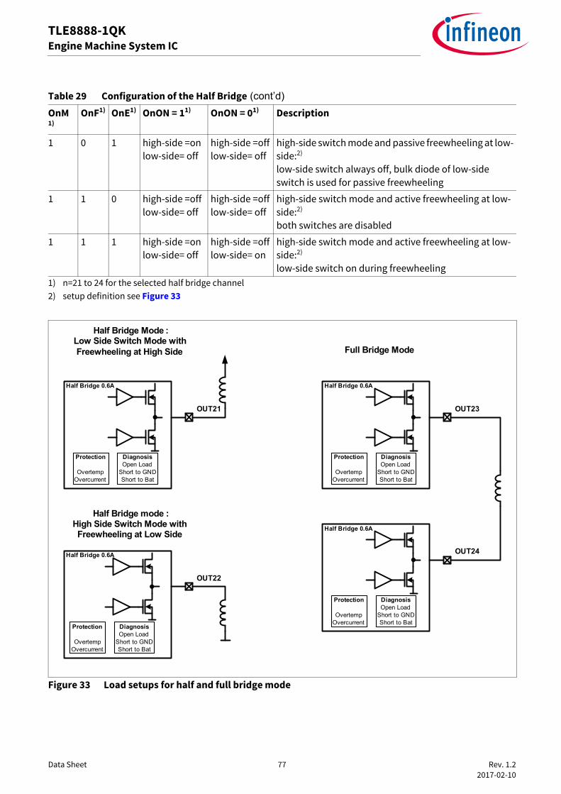
Data Sheet 77 Rev. 1.2 2017-02-10
TLE8888-1QKEngine Machine System IC
Figure 33 Load setups for half and full bridge mode
1 0 1 high-side =onlow-side= off
high-side =offlow-side= off
high-side switch mode and passive freewheeling at low-side:2)
low-side switch always off, bulk diode of low-side switch is used for passive freewheeling
1 1 0 high-side =offlow-side= off
high-side =offlow-side= off
high-side switch mode and active freewheeling at low-side:2)
both switches are disabled
1 1 1 high-side =onlow-side= off
high-side =offlow-side= on
high-side switch mode and active freewheeling at low-side:2)
low-side switch on during freewheeling1) n=21 to 24 for the selected half bridge channel2) setup definition see Figure 33
Table 29 Configuration of the Half Bridge (cont’d)OnM1)
OnF1) OnE1) OnON = 11) OnON = 01) Description
OUT21
Protection
OvertempOvercurrent
DiagnosisOpen Load
Short to GNDShort to Bat
Half Bridge 0.6A
OUT22
Protection
OvertempOvercurrent
DiagnosisOpen Load
Short to GNDShort to Bat
Half Bridge 0.6A
OUT23
Protection
OvertempOvercurrent
DiagnosisOpen Load
Short to GNDShort to Bat
Half Bridge 0.6A
OUT24
Protection
OvertempOvercurrent
DiagnosisOpen Load
Short to GNDShort to Bat
Half Bridge 0.6A
Half Bridge Mode :Low Side Switch Mode with Freewheeling at High Side
Half Bridge mode :High Side Switch Mode with Freewheeling at Low Side
Full Bridge Mode

Data Sheet 78 Rev. 1.2 2017-02-10
TLE8888-1QKEngine Machine System IC
9.7.1 Protection of Half Bridges OUT21 to OUT24The half bridge outputs are fully protected against overcurrent and overtemperature.In failure case (e.g. short to GND) the affected transistor is switched off after the “Overcurrent Switch OffFilter Time” and the diagnosis bit is set. The half bridge output is high ohmic (tristate).To cover all failure conditions the overtemperature protection is implemented. After exceeding thetemperature threshold the half bridge outputs are switched off till the temperature is decreased by the“Overtemperature Hysteresis”.For the procedure to switch on an affected channel after failure condition see Chapter 9.2.
9.7.2 Diagnosis of Half Bridges OUT21 to OUT24For the half bridge outputs various diagnosis function are implemented. For short to battery and short to GNDin on diagnosis the protection function overcurrent is used (diagnosis bits O21OC to O24OC in diagnosisregister BriDiag1). Overtemperature is signalized with the diagnosis bits B1OT and B2OT in diagnosis registerBriDiag1. For open load and short to GND (SCG) in off a special circuit is implemented. The diagnosis bitsO21DIA to O24DIA in diagnosis register BriDiag0 are set according the setup of the channels and accordingthe priority shown in Table 30.
Figure 34 Open Load and Short to GND/Battery Detection Circuit for Half Bridge Configuration (Low- or High-Side Load)
+
-
+
-
+
-Vol,high
Vol,low
BATPx
OnDIAG0
OnDIAG1 Dec
oder

Data Sheet 79 Rev. 1.2 2017-02-10
TLE8888-1QKEngine Machine System IC
Figure 35 Open Load and Short to GND/Battery Detection Circuit for Full Bridge Configuration
In Figure 36 and Figure 37 the behavior of the output current as a function of the output voltage in thedifferent configurations are shown.The detection in off for open load is the same for both settings but for the short detection there is a differencefor low-side and high-side switch mode.• Hig-side switch mode: short to battery detection in off• Low-side switch mode: short to GND detection in off
Figure 36 Output Behavior in Off for Low-Side Switch Configuration with Open Load and Short to GND Detection
+
-
+
-
+
-Vol,high
Vol,low
BATPx
+
-
+
-Vol,high
Vol,low
BATPx
OnDIAG0
OnDIAG1 Dec
oder
OmDIAG0
OmDIAG1Dec
oder
IOUTn
0
Idiag,pu min
VBATVOUTn_BIAS VOUTn
O.K.OLSCG
Vol,highVol.low
Idiag,pu max
Idiag,pd max
Idiag,pd min
Low Side Switch Mode

Data Sheet 80 Rev. 1.2 2017-02-10
TLE8888-1QKEngine Machine System IC
Figure 37 Output Behavior in Off for High-Side Switch Configuration with Open Load and Short to Battery Detection
Figure 38 Output Behavior in Off for Full Bridge Mode Configuration
The detection is active if the high-side and the low-side switch are off and the diagnosis activation timertbr,diag,act starts counting. For activation of the open load in off detection in active freewheeling configurationthe half bridge must be disabled by setting the bits O21E to O24E of configuration register OEConfig2 to“low”, for passive freewheeling a normal off signal (IN9 to IN12 or O21ON to O24ON in control register Cont2is set to “low”) is sufficient. For full bridge mode both half bridges must be off or disabled regarding the settingof the half bridge. After the Bridge Diagnosis Activation Time tbr,diag,act the output of the detection circuit isstored in the diagnosis register BriDiag0 according the priority shown in Table 30. After activation of the openload in off detection a filter time tbr,diag,f to suppress disturbances is implemented. The diagnosis register bitsare set after the specified filter times. With the readout of the diagnosis register the content is updated to theactual diagnosis.In Table 30 the definition of the diagnosis bits for single switch usage is defined, in Table 31 the definition forfull bridge mode.
Note: especially for full bridge mode it is recommended to read out the diagnosis register twice due to transition states and possible misleading diagnosis register entries
IOUTn
0
Idiag,pu min
VBATVOUTn_BIAS VOUTn
O.K. OL SCB
Idiag,pu max
Idiag,pd max
Idiag,pd min
High Side Switch Mode
Vol,highVol.low
IOUTn
0
Idiag,pu min
VBATVOUTn_BIAS VOUTn
OnDIAG[1:0]=01 OnDIAG[1:0]=00 OnDIAG[1:0]=10
Idiag,pu max
Idiag,pd max
Idiag,pd min
Full Bridge Mode
Vol,highVol.low

Data Sheet 81 Rev. 1.2 2017-02-10
TLE8888-1QKEngine Machine System IC
Note: For high-side switch mode (low-side load) after start up there will be a short to ground detection before the output is configured to high-side load and the diagnosis bits are set to “11”. This detection is not right and it is recommended to read out the diagnosis registers twice after start up to avoid wrong diagnosis information.
9.7.3 Electrical Characteristics Half Bridges
Table 30 Description of Diagnosis Information Single Switch UsageOnDIAG[1:0]1)
1) n from 21 to 24
Priority(1 = highest priority)
High-Side Switch Mode Low-Side Switch Mode
00 3 no failure no failure
01 2 open load in off n.a.
10 2 n.a. open load in off
11 1 short circuit to battery in off short circuit to ground in off
Table 31 Description of Diagnosis Information in Full Bridge ModeOnDIAG[1:0]1)
1) n = 21 and m=22 or n=23 and m=24
OmDIAG[1:0]1) Full Bridge Mode00 00 no failure
Single Failure00 01 open load in off (or double fault open load and short to GND at
OUT22 /OUT24)
10 10 short circuit to battery in off
01 01 short circuit to ground in off (or double fault open load and short to GND at OUT21 /OUT23
Double Failure00 10 open load and short circuit to bat at OUT22 /OUT24 in off
01 10 short circuit to ground at OUT21 /OUT23 and short circuit to battery at OUT22 /OUT24 in off
10 01 short circuit to battery at OUT21 /OUT23 and short circuit to ground or open load at OUT22 /OUT24 in off
Remaining Combinations10 00 not existing or transition states after switch off
xx 11
11 xx
01 00

Data Sheet 82 Rev. 1.2 2017-02-10
TLE8888-1QKEngine Machine System IC
Table 32 Electrical Characteristics Half BridgesVS = 13.5 V, VVSV = 5 V, Tj = -40°C to +150°C, all voltages with respect to GND, positive current flowing into pin,(unless otherwise specified)
Parameter Symbol Values Unit Note or Test Condition
NumberMin. Typ. Max.
OUT21…24, n = 21 to 24Operation Current IOUTn – – 0.6 A P_9.1
Overcurrent Switch Off Threshold IOUTn,oc 0.6 – 1.5 A P_9.2
Overcurrent Switch Off Filter Time toc,f 0.5 – 2 µs P_9.3
On Resistance ROUTn,on – 2.4 Ω IOUTn = 0.3 A P_9.4
OUT21 On Resistance at Low Battery Voltage, low temperature
ROUT21,on,l
,LT
– 2.4 Ω IOUTn = 0.1 A, VBAT = 4.5 VTj < 100°C
P_9.5
OUT21 On Resistance at Low Battery Voltage, high temperature
ROUT21,on,l
,HT
– 2.6 Ω IOUTn = 0.1 A, VBAT = 4.5 VTj > 100°C
P_9.6
Leakage Current, low-side IOUTn,l,low
– – 201)
1) In operation leakage current covered by open load current
µA VOUTn = 13.5 V P_9.7
Leakage Current, high-side IOUTn,l,high
-201) – – µA VOUTn = 0 V P_9.8
Turn On Delay Time2) td,on – – 10 µs IOUTn = 0.3 A, resistive load
P_9.9
Turn Off Delay Time2) td,off 0.1 – 10 µs IOUTn = 0.3 A, resistive load
P_9.10
Switch On Time2) ts,on 0.9 – 2.5 µs IOUTn = 0.3 A, resistive load
P_9.11
Switch Off Time2) ts,off 0.9 – 2.5 µs IOUTn = 0.3 A, resistive load
P_9.12
Diagnosis OUT21 to 24Overtemperature Switch Off Threshold
TOUTn,ot 150 – 200 °C 3) P_9.13
Overtemperature Hysteresis TOUTn,ot,hy
s
– 10 – °C 3) P_9.14
Open Load in Off Detection Threshold High Limit
Vol,high 0.9*V5V-0.2
0.9*V5V
0.9*V5V+0.2
V P_9.15
Open Load in Off Detection Threshold Low Limit
Vol, low 0.5*V5V-0.2
0.5*V5V
0.5*V5V+0.2
V P_9.16
Diagnosis Pull Up Current Idiag,pu -980 – -220 µA P_9.17
Diagnosis Pull Down Current Idiag,pd 150 – 300 µA P_9.18
Bridge Diagnosis Activation Time tbr,diag, act 60 – 135 µs P_9.19
Bridge Diagnosis Filter Time tbr,diag, f 0.5 – 2 µs P_9.20

Data Sheet 83 Rev. 1.2 2017-02-10
TLE8888-1QKEngine Machine System IC
2) see Figure 31 for timing definition3) not subject to production test, specified by design

Data Sheet 84 Rev. 1.2 2017-02-10
TLE8888-1QKEngine Machine System IC
9.8 Push Pull Stages OUT8 to OUT13 and DFB8 to DFB13These 5 V push pull stages are designed for driving on-board MOSFETs. The outputs are fully protected andvarious diagnosis functions are implemented.They are controlled and enabled like all power stages according the description in Chapter 9.1 andChapter 9.2. In off (“0” in control register or “low” at the configured direct drive input pin) the low-sidetransistor of the push/pull stage is on and forces a “low voltage level at the pin.
9.8.1 Protection of OUT8 to OUT13There are functions implemented to detect short to battery at the external MOSFET and to protect the driveroutputs.For the short to battery detection feedback pins DFB8 to DFB13 are implemented to sense the voltage at thedrain of the external MOSFET. The short to battery detection in on is done by comparing the voltage level ofthe drain feedback pins with the short to bat detection threshold.A short is detected after the “Short to Battery Detection Filter Time”. In case of short to battery the outputis switched off and the corresponding diagnosis bits in the diagnosis register OutDiag1 to OutDiag3 are setaccording the priority shown in Table 33. There are four different thresholds, “Short to Battery DetectionThreshold in On 1” to “Short to Battery Detection Threshold in On 4”, implemented so that the detectionthreshold can be adapted to the used MOSFET. The diagnosis of the push pull stages can be set in threegroups. The configuration is done with the bits PP0D to PP2D in the configuration register OutConfig2 andOutConfig3.The protection of the driver output pins is done by comparing the output voltage on the pins OUT8 to OUT13with the “Overvoltage Detection Threshold”. An overvoltage (e.g. short to battery) is detected after the“Overvoltage Diagnosis Filter Time” and the corresponding diagnosis bits in the diagnosis registerPPOVDiag is set. In case of overvoltage high and low-side transistors of the push pull driver are switched off(high ohmic state).
9.8.2 Diagnosis of OUT8 to OUT13For the push pull stages OUT8 to OUT13 various diagnosis functions for the external MOSFETs areimplemented. The open load, short to ground in off and short to battery in on detection is done via the drainfeedback DFB8 to DFB13. The diagnosis pull down current of the open load/short to ground in off detectioncan be switched off (see configuration register OutConfig2). With deactivated pull down current open load inoff detection is not active and the diagnosis information of OnDIAG[1:0] = 10B will never occur. Withdeactivated pull down current the short to ground detection is active.In Figure 39 the behavior of the output current as a function of the output voltage is shown.

Data Sheet 85 Rev. 1.2 2017-02-10
TLE8888-1QKEngine Machine System IC
Figure 39 Output behavior in off with open load and short to GND detection of DFB8 to DFB13
Whenever the push pull stages are off the open load/short to GND detection circuit is enabled. To suppressdisturbances the output of the detection circuit is stored in the diagnosis register OutDiag1 to OutDiag3 afterthe Diagnosis Filter Time for Open Load and Short to GND in Off Detection tdiag,f and according the priorityshown in Table 33. With the readout of the diagnosis register the content is updated to the actual diagnosis.
9.9 Electrical Characteristics Push Pull Stages OUT8 to OUT13
Table 33 Description of Diagnosis Information (DFB8 to DFB13)OnDIAG[1:0] Priority
(1 = highest priority)
Description
00 4 no failure
01 1 short circuit to battery
10 2 open load in off1)
1) no open load in off detection with deactivated pull down current11 3 short circuit to ground in off
Table 34 Electrical Characteristics Push Pull Stages OUT8 to OUT13Stages on or off, VS = 13.5 V, VVSV = 5 V, Tj = -40°C to +150°C, all voltages with respect to GND, positive currentflowing into pin, (unless otherwise specified)
Parameter Symbol Values Unit Note or Test Condition
NumberMin. Typ. Max.
OUT8…13, n = 8 to 13High Level Output Voltage VOUTn,h 4 – 5.5 V IOUTn = -5 mA P_9.8.1
Low Level Output Voltage VOUTn,l – – 0.6 V IOUTn = 5 mA P_9.8.2
Pull up current IOUTn,pu – – -20 mA VOUTn = 0 V, OUTn on
P_9.8.3
Pull down current IOUTn,pd 20 – – mA VOUTn = 5 V, OUTn off
P_9.8.4
pull up and down current active
pull down current switched off
IOUTn
0
Idiag,pu min
VBATVOUTn_BIAS VOUTn
O.K.OLSCG
VolVscg
Idiag,pu max
Idiag,pd max
Idiag,pd min
pull down current switched off
O.K.SCG
IOUTn,l

Data Sheet 86 Rev. 1.2 2017-02-10
TLE8888-1QKEngine Machine System IC
9.10 Push Pull Stages IGN1 to IGN4The IGN1 to IGN4 are 5 V push pull stages for on- and off-board ignition power stages (e.g. with IGBTs,darlington transistors). For off board ignition power stages the outputs IGN1 to IGN4 are equipped with aback supply suppression (in case of a short circuit from IGN1 to IGN4 to battery there is no parasitic currentflow back to 5 V).They are controlled and enabled like all power stages according the description in Chapter 9.1 andChapter 9.2. Additionally a “high” at the pin IGNEN is needed to enable the outputs. In off (“0” in controlregister or “low” at the configured direct drive input pin or IGNEN is “low”) the low-side transistor of thepush/pull stage is on and forces a “low voltage level at the pin.The outputs are fully protected and various diagnosis functions are implemented.
9.10.1 Protection of IGN1 to IGN4The protection of the outputs is done by detecting short to battery and short to ground. This is done bycomparing the output voltage level with the “Short to Battery Detection Threshold and Short to Ground
Overvoltage Detection Threshold VOUTn,ov,th 5.5 – 7.7 V P_9.8.5
Overvoltage Diagnosis Filter Time tOUTn,ov,f 5 – 10 µs P_9.8.6
Diagnosis DFB8 to DFB13Short to Battery Detection Threshold in On 1
VDFBn,sb,1 90 125 150 mV referred to PGND P_9.8.7
Short to Battery Detection Threshold in On 2
VDFBn,sb,2 180 225 250 mV referred to PGND P_9.8.8
Short to Battery Detection Threshold in On 3
VDFBn,sb,3 350 400 450 mV referred to PGND P_9.8.9
Short to Battery Detection Threshold in On 4
VDFBn,sb,4 0.7 0.8 0.9 V referred to PGND P_9.8.10
Short to Battery Detection Filter Time
VDFBn,sb,fl 10 – 15 µs P_9.8.11
Open Load in Off Detection Threshold
Vol V5V-0.2
V5V V5V+0.2
V P_9.8.12
Short to GND in Off Detection Threshold
Vscg 0.5*V5V-0.2
0.5*V5V
0.5*V5V+0.2
V P_9.8.13
Diagnosis Pull Down Current in Off Idiag,pd 220 – 600 µA VDFBn = 13.5 V P_9.8.14
Diagnosis Pull Up Current in Off Idiag,pu -300 – -100 µA VDFBn = 0 V P_9.8.15
Diagnosis Filter Time for Open Load and Short to GND in Off Detection
tdiag,f,off 60 – 135 µs P_9.8.16
Pull Down Current in On Idiag,pd,on – – 1.8 µA VDFBn = 5 V P_9.8.17
Table 34 Electrical Characteristics Push Pull Stages OUT8 to OUT13 (cont’d)Stages on or off, VS = 13.5 V, VVSV = 5 V, Tj = -40°C to +150°C, all voltages with respect to GND, positive currentflowing into pin, (unless otherwise specified)
Parameter Symbol Values Unit Note or Test Condition
NumberMin. Typ. Max.

Data Sheet 87 Rev. 1.2 2017-02-10
TLE8888-1QKEngine Machine System IC
Detection Threshold”. To suppress disturbances the output signal of the short to GND and short to batterydetection circuit is stored in the diagnosis register IgnDiag after the “Diagnosis Filter Time for Short to GNDand Battery Detection” tdiag,f,sc and according the priority shown in Table 35.During detected short to GND the output is switched off (low-side transistor of push/pull stage is on), duringdetected short to battery the output is high ohmic (tristate).The short to battery detection is always active. The short to ground detection is enabled with the on signal ofthe output stage.Additionally an overtemperature protection is implemented. There is one common sensor for IGN1 and IGN2and one for IGN3 and IGN4.
9.10.2 Diagnosis of IGN1 to IGN4An open load detection during the switch on phase is implemented and can be enabled with the bit IOLA inthe configuration register IGNConfig. In Figure 40 the detection principle is shown. When the open loaddetection in on is enabled, first the output is pulled up by a defined current, which is set by the bits IOLI in theconfiguration register IGNConfig.The output voltage, which is passed to the detection circuit, is filtered (“Diagnosis Filter Time for Open LoadDetection”) to suppress disturbances. After the open load time (“Open Load Time 1” to “Open Load Time4“selected in configuration register IGNConfig bits IOLT) the filtered output is compared with the Open LoadDetection Threshold Vol. The diagnosis register IgnDiag is set if the filtered output is higher than the OpenLoad Detection Threshold and the output is fully switched on.The failures are stored in the diagnosis register according the priority shown in Table 35 with “1” is the highestpriority. With the readout of the diagnosis register IgnDiag the content is updated to the actual diagnosis.
Table 35 Description of Diagnosis Information (IGN1 to IGN4)IGNnDIAG[1:0] Priority
(1 = highest priority)
Description
00 4 no failure
01 1 short circuit to battery or overtemperature
10 2 open load
11 3 short circuit to ground in on

Data Sheet 88 Rev. 1.2 2017-02-10
TLE8888-1QKEngine Machine System IC
Figure 40 Ignition Output Open Load Detection
9.11 Electrical Characteristics Push Pull Stages IGN1 to IGN4
Table 36 Electrical Characteristics Push Pull StagesStages on or off, VS = 13.5 V, VVSV = 5 V, Tj = -40°C to +150°C, all voltages with respect to GND, positive currentflowing into pin, (unless otherwise specified)
Parameter Symbol Values Unit Note or Test Condition
NumberMin. Typ. Max.
IGN1…4, n = 1 to 4High Level Output Voltage VIGNn,h 4.35 – – V IIGNn = -15 mA, P_9.9.1
Low Level Output Voltage VIGNn,l – – 0.6 V IIGNn = 5 mA P_9.9.2
Pull up current IIGNn,pu – – -20 mA VIGNn = 0 V, IGNn on P_9.9.3
Pull down current IIGNn,pd 20 – – mA VIGNn = 5 V, IGNn off P_9.9.4
Leakage current IL_IGNn – – 120 µA VIGNn = 13.5 V P_9.9.5
Leakage current to V5V IL_IGNn,V5V – – 1 µA VIGNn = 13.5 V P_9.9.26
Overtemperature Switch Off Threshold
TIGNx,ot 150 – 200 °C 1) P_9.9.6
Overtemperature Hysteresis TIGNx,ot,hys 10 °C 1) P_9.9.7
Diagnosis IGN1 to IGN4Short to Battery Detection Threshold
VIGNn,scb 6.4 – 7.5 V P_9.9.8
Short to Ground Detection Threshold
Vscg 1.6 – 2.3 V P_9.9.9
Diagnosis Filter Time for Short to GND and Battery Detection
tdiag,f,sc 5 – 10 µs P_9.9.10
t
VIGN
t
-IIGN
tol
OFF ON
Vol
Iol
open load measurement capturing of open load measuring result

Data Sheet 89 Rev. 1.2 2017-02-10
TLE8888-1QKEngine Machine System IC
Open Load Detection Threshold Vol 4 – 4.5 V P_9.9.11
Open Load Switch On Current 1 Iolf,1 -120 -100 -40 µA P_9.9.12
Open Load Switch On Current 2 Iolf,2 -500 -400 -300 µA P_9.9.13
Open Load Switch On Current 3 Iolf,3 -1.2 -1 -0.4 mA P_9.9.14
Open Load Switch On Current 4 Iolf,4 -5 -4 -2.5 mA P_9.9.15
Open Load Time 1 tol,1 50 60 70 µs P_9.9.16
Open Load Time 2 tol,2 210 250 290 µs P_9.9.17
Open Load Time 3 tol,3 450 510 570 µs P_9.9.18
Open Load Time 4 tol,4 690 775 860 µs P_9.9.19
Diagnosis Filter Time for Open Load Detection
tdiag,f,olf 6 10 14 µs P_9.9.20
Direct Drive Inputs IGNENLow Level Input Voltage VIN,l -0.3 – 0.9 V P_9.9.21
High Level Input Voltage VIN,h 2 – VVDDIO V P_9.9.22
Input Voltage Hysteresis VIN,hys 50 200 – mV P_9.9.23
Pull Down Current IIN,pd 25 – 100 µA VIN = VVDDIO P_9.9.24
Pull Down Current IIN,pd 2.4 – – µA VIN = 0.6 V P_9.9.251) Parameter is not subject of production test, specified by design
Table 36 Electrical Characteristics Push Pull Stages (cont’d)Stages on or off, VS = 13.5 V, VVSV = 5 V, Tj = -40°C to +150°C, all voltages with respect to GND, positive currentflowing into pin, (unless otherwise specified)
Parameter Symbol Values Unit Note or Test Condition
NumberMin. Typ. Max.

Data Sheet 90 Rev. 1.2 2017-02-10
TLE8888-1QKEngine Machine System IC
VR and Hall Sensor Interface
10 VR and Hall Sensor InterfaceThe variable reluctance (VR) sensor interface converts an output signal of a VR sensor into a push-pull logiclevel signal suited for microcontroller input ports. To achieve the best accuracy for the positive and thenegative edge of the VROUT signal the switching point is the zero crossing. For robustness againstdisturbances the next zero crossing is enabled only if a signal peak (minimum or maximum of the signal) isdetected. The amplitude of the VR sensor signal is limited by an internal clamping circuit to avoid damage ofthe device due to overvoltage caused by the VR sensor signal.There are three operation modes for VR sensor applications and one Hall sensor mode implemented. Themanuel VR sensor mode with static setup of the detection parameter under control of the microcontroller viaMSC/SPI and an auto mode with an adaptive algorithm to ensure best detection performance. The semi automode is less accurate then the auto mode.The diagnosis VR sensor interface setup could be done by measuring the voltage between the two input pinsduring diagnosis mode. Additionally three diagnosis bits for short to battery, short to GND and open load(directly at the pins) are available.
Figure 41 VR Sensor Interface Block diagram
10.1 Signal DetectionThe signal detection for Hall sensor mode is a comparator with the switching threshold VVRIN1,th, hall andthe hysteresis VVRIN1,hys, hall. The detection of the VR signal consist of the zero crossing detection, peakdetection and the output filter. At the input there is a clamping circuit between the pins VRIN1 and VRIN2suited to clamp the maximum current of VR sensors.The zero crossing detection ensures that the influence of the input signal slope is eliminated for both edges.To avoid disturbances due to the floating input signal a middle voltage is applied with the integrated loadresistance. The clamping circuit between the pins VRIN1 and VRIN2 clamps the input voltage in bothdirection to protect the input structures. The clamping is suited for VR sensors with a maximum output currentof ΔIVR,clamp (see Table 37).The peak detection is done by measuring the voltage difference by the analog to digital converter and thedetection of the slope of the input signal. If the gradient of the slope changes the sign the next zero crossingdetection is enabled. The detection of the sign is done by comparing the absolute value of the signal with the
DifferentialAmplifier
Comparator
Low Pass Filter
Peak & Time Measurement
ADC
Cla
mpi
ng
VRIN1
VRIN2
VROUT
Diagnosis on
Diagnosis on
Vmiddle
MSC/SPI
Detection&
Output Filter&
Diagnosis
VDDIORVR,Load/2
RVR,Load/2

Data Sheet 91 Rev. 1.2 2017-02-10
TLE8888-1QKEngine Machine System IC
VR and Hall Sensor Interface
peak detection threshold (VVR,peak,min,1 to VVR,peak,min,4 according setup). A sign change is only validif the absolute value of the signal is larger than peak detection threshold (VVR,peak,min,1 toVVR,peak,min,4 according setup) for a time longer than the peak detection time tVR,peak,min,1 totVR,peak,min,2 according setup (see Figure 42).
Figure 42 Timing Characteristics of the VR Sensor Interface
The output filter is implemented for all operation modes to suppress disturbances with high frequencies. Thefunction is shown in Figure 43. The output signal VROUT is filtered with the time tof,1. The output signal ofthe internal zero crossing detection must be stable for a time longer than tof,1.
Figure 43 Output Filter Behavior
Following parameters could be set by MSC/SPI communication:• peak detection threshold VVR,peak,min,1 to VVR,peak,min,4 with the bits VRSPV in the configuration
register VRSConfig0
VVR_OUT
t
t
t of tof
VVR_IN1 – VR_IN2
VVR, th=0V
50%
VVR,peak,min
-VVR ,peak,min
tVR,peak > tVR,peak,min tVR,peak < tVR,peak,min
tVR,peak > tVR,peak,min
|VVR,peak| < VVR,peak,min t of
VVRIN1-VRIN2
t
t
t < tof
tof
VVROUT
t < tof

Data Sheet 92 Rev. 1.2 2017-02-10
TLE8888-1QKEngine Machine System IC
VR and Hall Sensor Interface
• peak detection time tVR,peak,min,1 to tVR,peak,min,2 with the bit VRSPT in the configuration register VRSConfig0
• output filter time tof,1 to tof,4 with the bits VRSF in the configuration register VRSConfig0
10.2 Detection ModesThe TLE8888-1QK integrates four detection modes:• auto detection mode for VR sensor signals• manual detection mode for VR sensor signals• semi auto detection mode for VR sensor signals• detection mode for Hall sensor signalsTo select the various detection modes the bits VRSM in the configuration register VRSConfig1 must be set.Auto detection mode for VR sensor signals: In the auto detection mode an algorithm is setting all parametersto the optimal values to achieve the best detection behavior. The peak detection time is set due to the actualspeed value, the peak detection threshold is set due to the level of the previous peaks. The output filter time(tof,1 to tof,4) is set by the microcontroller independently to increase the robustness against shortdisturbances at the inputs. Write access to the registers bits of VRSPT and VRSPV are ignored in auto detectionmode.Semi auto detection mode for VR sensor signals: The algorithm of the semi auto mode is based on less numberof measurement information as the auto detection mode. This leads to a simpler implementation of thedetection algorithm. The output filter time (tof,1 to tof,4) is set by the microcontroller independently toincrease the robustness against short disturbances at the inputs. Write access to the registers bits of VRSPTand VRSPV are ignored in semi auto detection mode.Manual detection mode for VR sensor signals: In the manual detection mode the microcontroller has the fullcontrol of all parameters of the detection and the algorithm of the auto detection modes are disabled. Thesettings are done via the MSC/SPI interface.Detection mode for Hall sensor signals: For the Hall sensor mode the pin VRIN2 is forced internally to theswitching threshold VVRIN1,th, hall. The detection principle is a comparator with hysteresis. Write access tothe registers bits of VRSPT and VRSPV are ignored in the detection mode for Hall sensor signals. The diagnosisis disabled. With this set up the number of external devices is reduced (see Chapter 17.2).
Note: Switching between the different configurations must be avoided with active signals at the inputs VRIN1 and VRIN2.
10.3 Diagnosis for VR Sensor Signal Detection ModesThe TLE8888-1QK integrates three different diagnosis modes for the VR sensor interface:• short to GND/short to battery diagnosis mode: detection of short to GND or short to battery directly at pins
VRIN1 and VRIN2• open load diagnosis mode: detection of open load directly at pins VRIN1 and VRIN2• ADC measurement mode: measurement of the voltage between the pins VRIN1 and VRIN2The modes are defined in the configuration register VRSConfig1 with the bits VRSDIAGM.
The diagnosis of the VR sensor is done by activating the diagnosis mode with the bits VRSDIAGM in theconfiguration register VRSConfig1 and starting diagnosis measurement with the bit VDIAGS in the commandregister Cmd0. With the activation of the VRS diagnosis mode at VRIN1 a pull up current source to the internalsupply and at VRIN2 a pull down current source is applied (current configuration with bits VRSI_SC for shortto GND/short to battery diagnosis mode, VRSI_OL for open load diagnosis mode and VRSI_ADC for ADC

Data Sheet 93 Rev. 1.2 2017-02-10
TLE8888-1QKEngine Machine System IC
VR and Hall Sensor Interface
measurement mode in the configuration registers VRSConfig1 and VRSConfig2).To avoid bad influence of thetime constants of the external circuitry the timing of the measurement is controlled by the microcontroller.The sequence is shown in Figure 44.
The end of the diagnosis procedure triggered by the start command is signalized by the correspondent datavalid bits VRSDV_SC (short to GND and short to battery diagnosis mode), VRSDV_OL (open load diagnosismode) in diagnosis register VRSDiag0 and VRSDV_ADC (ADC measurement mode) in the diagnosis registerVRSDiag1.For the detection thresholds see parameter Short to GND detection threshold, Short to battery detectionthreshold and Open load detection threshold. The output of the ADC measurement is defined by theparameter ADC measurement gain and ADC measurement offset.The result of the diagnosis is available in the diagnosis register VRSDiag0 with the bits VRSG (short to GNDdetection), VRSB (short to battery detection) and VRSOL (open load detection directly at the pins). The digitalvalue of the ADC measurement is available in the register VRSDiag1 with the bits VRSD. This ADC value can beused by the microcontroller to define additional error detection conditions different to the defined short toGND, short to battery and open load thresholds.The data valid bits are reset with start of the corresponding diagnosis or with the readout of the register.
Note: In detection mode for Hall sensor signals the diagnosis is deactivated and the values of VRSDIAGM and VRSI_SCin the register VRSConfig1,VRSI_ADC and VRSI_OL in register VRSConfig2 and the start command VDIAGS in the register Cmd0 are ignored.

Data Sheet 94 Rev. 1.2 2017-02-10
TLE8888-1QKEngine Machine System IC
VR and Hall Sensor Interface
Figure 44 VRS Flow Chart
For the measurement the internal circuits are changed. In Figure 45, Figure 46 and Figure 47 the blockdiagram of the different setups are shown.
Diagnosis Mode Configuration
(Bits VRSDIAGM/VRSI_SC in Reg. VRSConfig1, Bits
VRSI_ADC/VRSI_OL in Reg. VRSConfig2)
Wait Phase
(till transisent effects can be neglected)
Start of Diagnosis Measurement
(Bit VDIAG in Reg. Cmd0)
Read out of Results
(Register VRSDiag0, VRSDiag1)
Data Valid Bits active?
End
No
Yes

Data Sheet 95 Rev. 1.2 2017-02-10
TLE8888-1QKEngine Machine System IC
VR and Hall Sensor Interface
Figure 45 VRS Diagnosis Block Diagram for Short to GND and Short to Battery Measurement
Figure 46 VRS Diagnosis Block Diagram for Open Load Measurement
Vamp,sc
ADC Compare
RVR,Load/2
RVR,Load/2
Idiag
Idiag
RegisterVRSDIAG0
Vmiddle
VRIN1
VRIN2Vth, scb
Vth, scg
Vamp,ADC
ADC
Idiag
Idiag
Compare RegisterVRSDIAG0Vmiddle
VRIN1
VRIN2
RVR,Load/2
RVR,Load/2
Vth, ol

Data Sheet 96 Rev. 1.2 2017-02-10
TLE8888-1QKEngine Machine System IC
VR and Hall Sensor Interface
Figure 47 VRS Diagnosis Block Diagram for ADC Measurement
Vamp,ADC
ADC RegisterVRSDIAG1
Idiag
Idiag
Vmiddle
Register VRSDIAG1 = (VRIN1-VRIN2)/VADC,LSB +VADC,offset
VRIN1
VRIN2
RVR,Load/2
RVR,Load/2
VADC

Data Sheet 97 Rev. 1.2 2017-02-10
TLE8888-1QKEngine Machine System IC
VR and Hall Sensor Interface
10.4 Electrical Characteristics VR Sensor Interface
Table 37 Electrical Characteristics: VR Sensor InterfaceVS = 13.5 V, VVSV = 5 V, Tj = -40°C to +150°C, all voltages with respect to ground, positive current flowing into pin(unless otherwise specified)
Parameter Symbol Values Unit Note or Test Condition
NumberMin. Typ. Max.
Input Characteristics:VR Sensor Interface Detection Threshold
VVR,th -30 0 30 mV P_10.4.1
minimum amplitude for peak detection 1
VVR,peak,min,1 – 50 – mV reset value P_10.4.2
minimum amplitude for peak detection 2
VVR,peak,min,2 – 150 – mV P_10.4.3
minimum amplitude for peak detection 3
VVR,peak,min,3 – 350 – mV P_10.4.4
minimum amplitude for peak detection 4
VVR,peak,min,4 – 550 – mV P_10.4.5
minimum time for peak detection 1
tVR,peak,min,1 – 10 – µs reset value1 kHz sinusoidal signal
P_10.4.6
minimum time for peak detection 2
tVR,peak,min,2 – 250 – µs 1 kHz sinusoidal signal
P_10.4.7
VR Sensor Interface Load Resistance
RVR,Load 50 75 110 kΩ P_10.4.9
VR Sensor Interface Input Clamping Current
ΔIVR,clamp – – 50 mA ΔIVR,clamp = (IVRIN1 -IVRIN2)/2
P_10.4.18
VR Sensor Interface Input Clamping Voltage
ΔVVR,clamp 2 – 3 V ΔVVR,clamp = |VVRIN1 -VVRIN”|,IVR,calmp = 50 mA
P_10.4.19
Switching threshold voltage at pin VRIN1 for Hall Sensor Mode
VVRIN1,th, hall 0.9 – 2 V no load at pin VRIN21)
P_10.4.20
Switching hysteresis pin VRIN1 for Hall Sensor Mode
VVRIN1,hys, hall 0.35 0.5 – V no load at pin VRIN2
P_10.4.10
Middle voltage level normal mode
Vmiddle 1.9 2.25 2.5 V P_10.4.11
VRS Diagnosis:Middle voltage level diagnosis mode
Vmiddle 0.9 1.3 1.65 V P_10.4.12
Diagnosis measurement time
tconv – 7 8 µs P_10.4.13

Data Sheet 98 Rev. 1.2 2017-02-10
TLE8888-1QKEngine Machine System IC
VR and Hall Sensor Interface
Diagnosis current accuracy Idiag, acc -30% – +30% VRIN1 = VRIN2 =Vmiddle;
typ. values see register VRSConfig1 and VRSConfig2
P_10.4.14
Short to GND detection threshold
Vth,scg 0.8 – 1.1 V P_10.4.15
Short to battery detection threshold
Vth,scb 2.8 – 3.3 V P_10.4.16
Open load detection threshold
Vth,ol 0.9 – 1.2 V P_10.4.17
ADC measurement input range
VADC,r -1.5 – 1.5 V P_10.4.8
ADC measurement gain VADC,LSB – 49 – mV valid from 6d to 70d P_10.4.31
ADC measurement offset VADC,offset – 37d – P_10.4.32
Output Characteristics:Low Level Output Voltage - Low Output Current
VVR_OUT,L,l – – 0.4 V IVR_OUT = 100 µA P_10.4.21
Low Level Output Voltage - High Output Current
VVR_OUT,L,h – – 1.5 V IVR_OUT = 1 mA P_10.4.22
High Level Output Voltage - Low Output Current
VVR_OUT,H,l VDDIO-0.4
– – V IVR_OUT = -100 µA P_10.4.23
High Level Output Voltage - High Output Current
VVR_OUT,H,h VDDIO-1.5
– – V IVR_OUT = -1 mA P_10.4.24
Transfer Characteristics:Output Filter Time 1 tof,1 1 2 3 µs reset value P_10.4.25
Output Filter Time 2 tof,2 5 6 7.5 µs P_10.4.26
Output Filter Time 3 tof,3 9.5 11 13 µs P_10.4.27
Output Filter Time 4 tof,4 19 21 23 µs P_10.4.281) external circuitry for hall mode see Chapter 17.2
Table 37 Electrical Characteristics: VR Sensor Interface (cont’d)VS = 13.5 V, VVSV = 5 V, Tj = -40°C to +150°C, all voltages with respect to ground, positive current flowing into pin(unless otherwise specified)
Parameter Symbol Values Unit Note or Test Condition
NumberMin. Typ. Max.

Data Sheet 99 Rev. 1.2 2017-02-10
TLE8888-1QKEngine Machine System IC
Local Interconnect Network (LIN)
11 Local Interconnect Network (LIN)The LIN interface is designed for in-vehicle networks using data transmission up to 20 kbit/s. Theimplementation of the physical layer is according to LIN specification revision 2.1 for slave nodes and iscompatible with lower versions like revision 2.0 and 1.31). LINTX is the transmit-data input from themicrocontroller, LINIO is the bidirectional LIN bus signal and LINRX is the receive-data output to themicrocontroller. The transmitted data stream at LINTX is converted to the LIN bus signal at LINIO. LINRXreflects the received data at LINIO with a logic signal suited for 3.3 V and 5 V microcontroller interfaces.The detection thresholds at LINIO are related to the power supply BATPA2).The LIN interface of the TLE8888-1QK is compatible to the physical layer definition of the K-Line (ISO 9141)standard. For K-Line operation no additional settings are necessary.A flash mode for high speed operation can be selected with the communication interface (MSC or SPI). Thereis no bus wake-up function implemented.
Figure 48 Local Interconnect Network (LIN) Slave Node
The LIN interface in the TLE8888-1QK is implemented according the requirements of the standard for slavenodes. For master setup an external pull up resistor (typ. 1 kΩ, see definition in LIN specification) and a diodemust be connected to LINIO and BATPA on the ECU (see Figure 49).
1) see LIN specification revision 2.1 chapter 6.22) BATPA is identical to the internal supply voltage VSUP defined in LIN specification revision 2.1
optional
BATPA
LINRX
RLIN
GND
LINIO
LINRX
LINTX
Dser,int
internal Logic
TLE8888 - LIN 2.1
LIN Bus
ECU in LIN Slave Configuration
BATECU
GNDECU
Micro Controller

Data Sheet 100 Rev. 1.2 2017-02-10
TLE8888-1QKEngine Machine System IC
Local Interconnect Network (LIN)
Figure 49 Local Interconnect Network (LIN) Master Node
11.1 Operation ModesThe interface can be configured for three operation modes:• LIN/K-Line Mode: operation according LIN specification revision 2.1 with a maximum speed of 20 kbit/s
and K-Line standard ISO 9141• Receive Only Mode: transmission of data is disabled• Flash Mode: operation up to 115 kbit/s is possible, slope control and current limitation are deactivatedThe selection of the modes is done with setting the bits LIN in the register ComConfig1 via communicationinterface (MSC or SPI). The operation mode after power on reset is defined by reset value of the register.
11.2 Failure Modes in LIN/K-Line OperationIn the LIN specification a special behavior of the interface is required for some failure conditions. This behavioris also active if a K-Line node is used.
11.2.1 Performance in Non Operation Supply Voltage RangeFor supply voltages out of operation range the interface may still operate, but communication is notguaranteed. For LINTX = ‘high’ (recessive) the interface shall not drive LINIO to dominant state and if LINIOis in recessive state the LINRX output shall provide a ‘high’ (recessive).
11.2.2 Loss of Supply Voltage and GND ConnectionDuring loss of supply voltage or GND connection the interface shall not interfere with the communication ofother LIN nodes. Upon return of connection, normal operation shall resume without any intervention on theLIN bus line (pin LINIO).
optional
BATPA
LINRX
RLIN,Slave
GND
LINIO
LINRX
LINTX
Dser,int
internal Logic
1kOhm
TLE8888 - LIN 2.1
LIN Bus
ECU in LIN Master Configuration
BATECU
GNDECU
Micro Controller

Data Sheet 101 Rev. 1.2 2017-02-10
TLE8888-1QKEngine Machine System IC
Local Interconnect Network (LIN)
11.2.3 Bus Wiring Short to Battery or GNDThe LIN interface is protected against short to battery or short to GND. Upon remove of the fault, normaloperation shall resume without any intervention on the LIN bus line (pin LINIO).
11.2.4 TX Time OutThe TX time out function is implemented to prevent the bus line from being blocked by a permanent ‘low’ atthe pin LINTX caused by an error at the ECU or the microcontroller. If the LINTX signal is ‘low’ (dominant) fort > ttimeout the transmission of the LINTX signal to the bus is deactivated and the LIN output stage is disabled.The transmission is reactivated, after a rising edge at LINTX was detected. The implemented time out featurerequires a minimum data rate of 1600 bit/s.The time out function can be disabled with the configuration bit LINTOE in the configuration registerComConfig1.
11.2.5 Overtemperature ProtectionThe LIN bus output LINIO is protected against overload with an overtemperature protection. In case ofovertemperature the output transistor is switched off and the diagnosis bit LINOT in the diagnosis registerComDiag is set. The configuration register is not changed.

Data Sheet 102 Rev. 1.2 2017-02-10
TLE8888-1QKEngine Machine System IC
Local Interconnect Network (LIN)
11.3 Electrical Characteristics LIN
Table 38 Electrical Characteristics: LINVS = 13.5 V, VVSV = 5 V, Tj = -40°C to +150°C, all voltages with respect to ground, positive current flowing into pin(unless otherwise specified)
Parameter Symbol Values Unit Note or Test Condition
NumberMin. Typ. Max.
Supply voltage range for normal operation
VBATPA,LIN 7 – 18 V acc. Param 10 LIN Spec. Rev. 2.1
P_11.3.1
Limitation Current at LINIO for driver dominant state
ILINIO,lim 40 – 200 mA acc. Param 12 LIN Spec. Rev. 2.1
P_11.3.2
Leakage Current at LINIO for bus dominant state and driver off
ILINIO,leak,dom -1 – – mA acc. Param 13 LIN Spec. Rev. 2.1VLINIO = 0 VVBAT = 12 V
P_11.3.3
Leakage Current at LINIO for bus recessive state
ILINIO,leak,rec – – 20 μA acc. Param 14 LIN Spec. Rev. 2.1VLINIO > VBAT
P_11.3.4
Current at LINIO during GND loss
ILINIO,no_GND -1 – 1 mA acc. Param 15 LIN Spec. Rev. 2.1GND = VS0 V < VLINIO < 18 VVBAT = 12 V
P_11.3.5
Current at LINIO during power supply loss
ILINIO,no_Sup – – 20 μA acc. Param 16 LIN Spec. Rev. 2.1GND = VS = 0 V0 V < VLINIO < 18 V
P_11.3.6
Receiver Dominant State VLINIO,dom – – 0.4*VB
ATPA
V acc. Param 17 LIN Spec. Rev. 2.1
P_11.3.7
Receiver Recessive State VLINIO,rec 0.6*VBATPA
– – V acc. Param 18 LIN Spec. Rev. 2.1
P_11.3.8
Receiver switching threshold center voltage
VLINIO,cnt 0.475*VBATPA
– 0.525*VBATPA
V acc. Param 19 LIN Spec. Rev. 2.1VLINIO,cnt = (Vth,
dom + Vth,rec)/2
P_11.3.9
Hysteresis of switching threshold
VHys – – 0.175*VBATPA
V acc. Param 20 LIN Spec. Rev. 2.1VHys = Vth,rec-Vth,dom
P_11.3.10
Voltage drop at internal serial diode Dser,int
VD 0.4 – 1 V acc. Param 21 LIN Spec. Rev. 2.1
P_11.3.11
Resistance of internal slave resistor Rslave
RLIN,Slave 20 – 60 kΩ acc. Param 26 LIN Spec. Rev. 2.1
P_11.3.12

Data Sheet 103 Rev. 1.2 2017-02-10
TLE8888-1QKEngine Machine System IC
Local Interconnect Network (LIN)
Duty cycle 1 D1 0.396 – – – acc. Param 27 LIN Spec. Rev. 2.1
P_11.3.13
Duty cycle 2 D2 – – 0.581 – acc. Param 28 LIN Spec. Rev. 2.1
P_11.3.14
Duty cycle 3 D3 0.417 – – – acc. Param 29 LIN Spec. Rev. 2.1
P_11.3.15
Duty cycle 4 D4 – – 0.59 – acc. Param 30 LIN Spec. Rev. 2.1
P_11.3.16
Propagation delay of receiver rising edge
trx,pd,r – – 6 μs acc. Param 31 LIN Spec. Rev. 2.1
P_11.3.17
Propagation delay of receiver falling edge
trx,pd,f – – 6 μs acc. Param 31 LIN Spec. Rev. 2.1
P_11.3.18
Propagation delay symmetry of receiver
trx,pd,sym -2 – 2 μs acc. Param 32 LIN Spec. Rev. 2.1
P_11.3.19
TX Dominant Time Out Time ttimeout 6 12 20 ms min. data rate of 1600bit/s required
P_11.3.20
Bus Recessive Output Voltage
VBUS,rec 0.8*VB
ATPA
– – V P_11.3.21
Bus Dominant Output Voltage
VBUS,do – – 1.4 V VBATPA = 7 VRpu = 500 Ω
P_11.3.22
Bus Dominant Output Voltage
VBUS,do – – 2.2 V VBATPA = 18 VRpu = 500 Ω
P_11.3.23
LINIO Input Capacitance CLINIO – 15 25 pF 1) P_11.3.24
Overtemperature Switch Off Threshold
TLIN,ot 150 – 200 1) P_11.3.25
Overtemperature Hysteresis TLIN,ot,hys – 10 – 1) P_11.3.26
LINRX Output CharacteristicsLow Level Output Voltage - Low Output Current
VLINRX,L,l – – 0.4 V ILINRX = 100 µA P_11.3.27
Low Level Output Voltage - High Output Current
VLINRX,L,h – – 1.5 V IVR_OUT = 1 mA P_11.3.28
High Level Output Voltage - Low Output Current
VLINRX,H,l VDDIO-0.4
– – V ILINRX = -100 µA P_11.3.29
High Level Output Voltage - High Output Current
VLINRX,H,h VDDIO-1.5
– – V ILINRX = -1 mA P_11.3.30
LINTX Input CharacteristicsLow Level Input Voltage VLINTX,l -0.3 – 0.9 V P_11.3.31
Table 38 Electrical Characteristics: LIN (cont’d)VS = 13.5 V, VVSV = 5 V, Tj = -40°C to +150°C, all voltages with respect to ground, positive current flowing into pin(unless otherwise specified)
Parameter Symbol Values Unit Note or Test Condition
NumberMin. Typ. Max.

Data Sheet 104 Rev. 1.2 2017-02-10
TLE8888-1QKEngine Machine System IC
Local Interconnect Network (LIN)
Figure 50 Timing Diagram of the LIN Interface
High Level Input Voltage VLINTX,h 2 – VVDDIO V P_11.3.32
Input Voltage Hysteresis VIN,hys 50 200 – mV P_11.3.33
Pull Up Current ILINTX,pu -100 – -25 µA VLINTX = 0 V P_11.3.34
Pull Up Current ILINTX,pu – – -2.4 µA VLINTX = VDDIO-0.6 V
P_11.3.35
1) Not subject to production test, specified by design
Table 38 Electrical Characteristics: LIN (cont’d)VS = 13.5 V, VVSV = 5 V, Tj = -40°C to +150°C, all voltages with respect to ground, positive current flowing into pin(unless otherwise specified)
Parameter Symbol Values Unit Note or Test Condition
NumberMin. Typ. Max.
VSVLINIO,rec
GNDt
t
VLINIO
LINTX
0.6 * VSVLIN,cnt
LINRX
Vth,rec
Vth,dom
trx,pd,f trx.pd,r
tBIT.dom
tBIT tBIT tBIT
VBAT
t
0.4 * VS
VLINIO,dom

Data Sheet 105 Rev. 1.2 2017-02-10
TLE8888-1QKEngine Machine System IC
High Speed Controller Area Network (CAN) Transceiver
12 High Speed Controller Area Network (CAN) TransceiverThe Controller Area Network (CAN) is a serial bus system that connects microcontroller, sensors and actuatorsfor real-time control applications. The integrated CAN interface provides the physical layer of the CAN according to ISO 11898. It is suitable forhigh speed differential data transmission and reception. It works as an interface between the CAN protocolcontroller and the physical bus lines.Remote wake-up function with a dominant signal at the bus lines is implemented.
12.1 Functional DescriptionThe high speed CAN is a two wire differential network which allows data transmission rates up to 1Mbit/s. Theinput CANTX and the output CANRX are connected to the microcontroller of the ECU. As shown in Figure 51,the CAN has a receive unit and a output driver stage, allowing the transceiver to send data to the bus line andmonitor data from the bus lines at the same time. It converts the serial data stream available at the transmitdata input CANTX into a differential output signal at CANH and CANL. The receiver stage monitors CANHand CANL and converts the differential voltage to a serial data stream at CANRX.The supply of the CAN transceiver is done out of V5VCAN, the wake receiver is supplied out of V5VSTBY. Thepin V5VCAN must be connected directly to the 5 V supply pin V5V. In order to optimize EMC performance aceramic capacitor CV5VCAN should be connected to the pins V5VCAN and PGND (pin 50).
Figure 51 High speed CAN topology
12.2 Operation ModesFour different operation modes are available. Regardless of the supply status the CAN interface does notdisturb the communication on the bus line.
CANH
CANL
ESD RDIV CMP RxD_BUF CANRX
TxD_BUF CANTXDRV
DIAG analog
Error Register
analog filter deglitcher
RL
Wake Receiver CANWK
V5VSTBYCANWKEN
MSC/SPI Interface SDO
SINWKCLR
V5VCAN
CAN Transceiver
RLCA
N
node
n
CAN node n-1
VDDIO

Data Sheet 106 Rev. 1.2 2017-02-10
TLE8888-1QKEngine Machine System IC
High Speed Controller Area Network (CAN) Transceiver
12.2.1 Normal Operation ModeIn normal operation mode the CAN transceiver sends the serial data stream available at the pin CANTX to theCAN bus while at the same time the data available at the CAN bus is monitored at the CANRX pin. In normaloperation mode all functions are active:• The driver output is active and drives data from the CANTX pin to the CAN bus.• The receiver unit is active and provides the data from the CAN bus to the CANRX pin.• The failure detection is active.
12.2.2 Receive Only ModeIn the receive only mode the CAN transceiver can still receive data from the bus, but the driver output stage isdisabled and therefore no data can be sent to the CAN bus. All other functions are active:• The driver output is disabled and data which is available at the CANTX pin will be blocked and not
communicated to the CAN bus.• The receiver unit is active and provides the data from the CAN bus to the CANRX pin.• The failure detection is active.
12.2.3 Power-Down ModeIf the TLE8888-1QK is not supplied the bus communication is not allowed to be disturbed. Therefore theresistors of the receiver unit are switched off and the bus input pins CANH and CANL are high resistive.
12.2.4 Remote Wake-UpThe wake receiver is internally supplied from the standby supply pin V5VSTBY. The wake-up function isenabled by an external connection of the pin CANWKEN to the standby supply pin V5VSTBY. The wakefunction is disabled by an external connection to AGND and the current consumption of the wake-up circuitis reduced to leakage currents only.In “ECU Sleep” state a dominant signal at CANH and CANL for longer than the CAN Wake-up filter timepreceded by a recessive signal causes an internal wake-up and the internal wake signal CANWK is set. With awake clear command (set bit WKCLR to “1” in command register Cmd0) CANWK is reset (status see bit CANWKin the status register OpStat0). The next wake-up is only detected with a transition from recessive todominant. With this implementation of the wake-up procedure, bus line dominant clamping does not lead topermanent wake-up.In Figure 52, Figure 53 and Figure 54 the behavior is shown.

Data Sheet 107 Rev. 1.2 2017-02-10
TLE8888-1QKEngine Machine System IC
High Speed Controller Area Network (CAN) Transceiver
Figure 52 CAN Remote Wake-up
Figure 53 CAN Wake-up State machine
CANHCANL
V5V
t
t
tdom < tWake tWake
wake up
CAN WakeCANWK=1
CANSleep
recessiveCANWK=0
CANWK=0
bus dominant > tWake
bus recessive & WKCLR=1
CANSleep
dominant
bus dominant &
WKCLR=1
bus
rece
ceive
after ramp up of V5VSTBY

Data Sheet 108 Rev. 1.2 2017-02-10
TLE8888-1QKEngine Machine System IC
High Speed Controller Area Network (CAN) Transceiver
Figure 54 State Transitions at CAN Remote Wake-up
12.3 Diagnostic FunctionsThe CAN transceiver has an implemented diagnostic unit. Bus failures and local failures can be detected.
12.3.1 CAN Bus Failure DetectionIn normal operation the CAN transceiver can detect following bus failure:• Bus line dominant clamping (bit CANBDC in diagnosis register ComDiag)Following bus failures can’t be detected (outputs are protected):• CANH shorted to GND• CANL shorted to GND• CANH shorted to low voltage supply• CANL shorted to low voltage supply• CANH shorted to VBat
• CANL shorted to VBat
• CANH open• CANL open• CANH shorted to CANL
12.3.2 Local Failure DetectionIn normal operation the CAN transceiver can detect following local failures:• CAN TX dominant time-out (bit CANTXTO in diagnosis register ComDiag)• Overtemperature (bit CANOT in diagnosis register ComDiag)In case of failure detection only the corresponding diagnosis register bits are changed. No change in theconfiguration occurs.
CAN Sleep recessive
CAN Wake CAN WakeStatus CAN Wake
Statemachine1)
CANHCANL
tCAN Sleep recessive CAN Sleep dominant CAN Sleep
recessive
Wake Up by CAN remote wake up ; KEY = EOTWK = WK = 0
CSNMSC Communication
tSet WKCLR=“1“
ECU Sleep ECU Sleep ECU Sleep
1) Wake Up Filter Time is not shown in the diagram
Set WKCLR=“1“

Data Sheet 109 Rev. 1.2 2017-02-10
TLE8888-1QKEngine Machine System IC
High Speed Controller Area Network (CAN) Transceiver
12.4 Electrical Characteristics CAN Transceiver
Table 39 Electrical Characteristics: CAN TransceiverVS = 13.5 V, VVSV = 5 V, Tj = -40°C to +150°C, all voltages with respect to ground, positive current flowing into pin(unless otherwise specified)
Parameter Symbol Values Unit Note or Test Condition
NumberMin. Typ. Max.
CANH voltage, recessive state
VCANH,rec 2 2.5 3 V no load P_12.4.1
CANL voltage, recessive state
VCANL,rec 2 2.5 3 V no load P_12.4.2
CANH voltage, dominant state
VCANH,dom 2.75 3.5 4.5 V P_12.4.3
CANL voltage, dominant state
VCANL,dom 0.5 1.5 2.25 V P_12.4.4
Differential output bus voltage, dominant state
Vdiff,out,dom 1.5 2 3 V 4.75 V < VV5VCAN < 5.25 V
P_12.4.5
Common mode bus voltage, dominant and recessive state
VCM -12 – 12 V 4.75 V < VV5VCAN < 5.25 V
P_12.4.6
External Termination resistor
RL 100 120 130 Ω P_12.4.7
Differential input voltage, recessive state
Vdiff,n,rec -1 – 0.5 V P_12.4.8
Differential input voltage, dominant state
Vdiff,in,dom 0.9 – 5 V P_12.4.9
Differential receiver hysteresis
Vdiff,hys 20 100 – mV P_12.4.10
Common mode input resistance
Rin 5 – 50 kΩ P_12.4.11
Bit time tB 1 – – μs P_12.4.12
Propagation delay time CANTX to CANRX recessive to dominant
tpd,rec,dom – – 255 ns P_12.4.13
Propagation delay time CANTX to CANRX dominant to recessive
tpd,dom,rec – – 255 ns P_12.4.14
Propagation delay time CANTX to CANH/CANL recessive to dominant
tpd,out,dom – – 140 ns Tj = 25°C;1) CCANH/CANL <10 pF
P_12.4.15
Propagation delay time CANTX to CANH/CANL dominant to recessive
tpd,out,rec – – 140 ns Tj = 25°C1); CCANH/CANL <10 pF
P_12.4.16

Data Sheet 110 Rev. 1.2 2017-02-10
TLE8888-1QKEngine Machine System IC
High Speed Controller Area Network (CAN) Transceiver
Bus line dominant clamping detection time
tbus,cl,dom 4 – 7 ms P_12.4.17
CANTX dominant detection time
tCANTX,cl,dom 4 – 7 ms P_12.4.18
V5VCAN buffer capacitance1)
CV5VCAN 2 – µF recommended for optimized EMC performance
P_12.4.19
Overtemperature Switch Off Threshold
TCAN,ot 150 – 200 °C 1) P_12.4.20
Overtemperature Hysteresis TCAN,ot,hys – 10 – °C 1) P_12.4.21
CANRX Output CharacteristicsLow Level Output Voltage - Low Output Current
VCANRX,L,l – – 0.4 V ICANRX = 100 µA P_12.4.22
Low Level Output Voltage - High Output Current
VCANRX,L,h – – 1.5 V ICANRX = 1 mA P_12.4.23
High Level Output Voltage - Low Output Current
VCANRX,H,l VDDIO-0.4
– – V ICANRX = -100 µA P_12.4.24
High Level Output Voltage - High Output Current
VCANRX,H,h VDDIO-1.5
– – V ICANRX = -1 mA P_12.4.25
CANTX Input CharacteristicsLow level input voltage VCANTX,l -0.3 – 1 V P_12.4.26
High level input voltage VCANTX,h 2 – VV5VCAN V P_12.4.27
Input voltage hysteresis VCANTX,hys 50 200 – mV P_12.4.28
Pull up current ICANTX,pu -100 – -25 µA VCANTX = 0 V P_12.4.29
Wake ReceiverDifferential input voltage, recessive state, low power mode
Vdiff,rec,lp -1 – 0.4 V 4.75V < VV5VSTBY < 5.25 V
P_12.4.30
Differential input voltage, dominant state, low power mode
Vdiff,dom,lp 1.15 – 5 V 4.75 V < VV5VSTBY < 5.25 V
P_12.4.31
Common mode bus voltage, low power mode
VCM,lp -12 – 12 V 4.75 V < VV5VSTBY < 5.25 V
P_12.4.32
CAN Wake-up filter time twake,CAN 0.75 – 5 μs 4.75 V < VV5VSTBY < 5.25 V
P_12.4.33
Additional current consumption in low power mode at pin BATSTBY
ICANWK – – 35 μA 0 V ≤ VCANH ≤ 5 V,0 V ≤ VCANL ≤ 5 V
P_12.4.34
Table 39 Electrical Characteristics: CAN Transceiver (cont’d)VS = 13.5 V, VVSV = 5 V, Tj = -40°C to +150°C, all voltages with respect to ground, positive current flowing into pin(unless otherwise specified)
Parameter Symbol Values Unit Note or Test Condition
NumberMin. Typ. Max.

Data Sheet 111 Rev. 1.2 2017-02-10
TLE8888-1QKEngine Machine System IC
High Speed Controller Area Network (CAN) Transceiver
1) Not subject to production test, specified by design

Data Sheet 112 Rev. 1.2 2017-02-10
TLE8888-1QKEngine Machine System IC
Microsecond Channel MSC
13 Microsecond Channel MSCThe bidirectional microsecond channel (MSC) is a serial interface which is especially optimized to connectperipheral devices via serial link to microcontroller. The serial communication link is built up by a fastsynchronous downstream channel from microcontroller to the device and an asynchronous upstreamchannel (referenced to downstream clock). The downstream interface can be “low voltage differential”(FCLN, FCLP, SIN, SIP, CSN) or “single ended” (FCLP, SIP, CSN).Via MSC, the microcontroller controls the outputs and logic of the device including the diagnosis andmonitoring module. Read data is requested by microcontroller via downstream communication and returnedby the device via MSC upstream channel.
Multiple “power devices” with MSC for downstream operation are possible. The device is selected by CSN.The MSC logic is internally supplied and referenced to AGND. The behavior of the MSC interface during reset is described in Table 5 and Table 6 in Chapter 5.2.
Figure 55 MSC Interface (not tested, overview only)
13.1 Downstream CommunicationDownstream frames are synchronous serial frames with clock and data line.The physical interface for downstream communication can be “low voltage differential” or “single ended”type. Both interface types are using individual pins (FCLN, FCLP, SIN and SIP) and common pins (CSN andSDO). For single ended interface FCLN and SIN have to be connected to VDDIO. For low voltage differentialinterface both input voltage levels must be within the defined input voltage range.The frames and the behavior of the communication are the same in differential and single ended mode.Differential inputs for downstream data are SIP and SIN; the differential input signal SIP – SIN is the samelogical signal as SIP alone in single ended mode and SI will be used in the description for both types ofcommunication. The clock pins are FCLP and FCLN, the differential clock FCLP – FCLN is the same logicalsignal as FCLP in single ended mode and CLK will be used in the description for both types of communication.There is one input CSN for chip select, and one output SDO for upstream data. The device is always the slavein this communication link.The CSN signal enables receiver circuits automatically during a downstream frame transmission. Two types of downstream frames are defined:
MSC interface
Asynchronous/synchronousreceive buffer
Microcontroller TLE8888
Downstream
Upstream
Shift register32 Bit
Chip select input(low activ)
Clock input
Serial data output
CSN
FCLP
FCLN Differential
DownstreamdataSIP
SIN
SDO
Figures_TLE8728.vsd
Single ended
Differential
Differential
Single ended
Differential

Data Sheet 113 Rev. 1.2 2017-02-10
TLE8888-1QKEngine Machine System IC
Microsecond Channel MSC
• Command frames (selection bit = “1”)• Data frames (selection bit = “0”)The device MSC uses non inverting polarity for SI and CLK: SI changes its state with the rising edge of CLK andis sampled with the falling edge; a logic ‘1’ is a ‘high level’ on SI, and a logic ‘0’ is a ‘low level’ on SI. Data at SIis latched by the device on the falling edge of CLK.The CSN input is active low during the active phases of command or data frames. An active enable signalvalidates the SI input signal. Outside the active phase (CSN line is at high level) data at SI is ignored.It is possible to drive multiple “power devices” with shared CLK and SI lines and individual CSN signal.Command frames and data frames may be sent in any sequence (with a passive phase of at least 2 CLK-cyclesafter each frame).
The serial clock CLK must be active (toggling) during upstream communication even when no commandframe or data frame is transmitted.The clock period of CLK is defined as tFCL, maximum downstream clock rate is fFCLmax.The active phase of a downstream frame starts with the falling edge of the signal on CSN and ends with therising edge. CSN changes its state with the rising edge of clock CLK.
Table 40 Execution of commandsEvent on MSC downstream upstream busy upstream idlevalid read command frame ignored executed
valid write command frame executed1)
1) only after tprep,sr or tprep,mr, see also Chapter 13.2
executed
valid data frame accepted accepted
invalid command ignored ignored
invalid data frame ignored ignored

Data Sheet 114 Rev. 1.2 2017-02-10
TLE8888-1QKEngine Machine System IC
Microsecond Channel MSC
Figure 56 Voltage level diagram
13.1.1 Downstream Supervisory FunctionsA command- or data frame is interpreted as valid, if it has the correct number of CLK pulses (a frame has alength of 17 clock pulses). Clock pulses are counted at the falling edge of the signal.There is no parity check.If TLE8888-1QK receives no valid data frame for t > tMSC_mon, the device switches off the output stages (alloutput stage control bits are set to “0”), the bits O1E to O24E in the configuration registers OEConfig0 toOEConfig3 are set to “0” and the MSC time out failure bit in the register ComDiag is set to “1”. The MSC timeout failure bit is reset by a readout of the register ComDiag and all output stages remain off. For switching onthe stages the bits O1E to O24E in the configuration registers OEConfig0 to OEConfig3 must be set to “1” andthe control bits must be set. Outputs which are configured to be driven directly with the direct drive inputs areswitched according the input level of the pins IN1 to IN12 after set of the bits O1E to O24E.
Drawing10_Voltage _level_diagram.vsd
This figure shows SIP and SIN function but is also valid for FCLP and FCLN
SIP
SINVSIN(min), VSIP(min)
VSIN(max), VSIP(max)
Not defined
Not defined
VSIx_low(min) VSIx_low(max)
Logic function
1 0 1
VSIN(min), VSIP(min)
VSIN(max), VSIP(max)
VSINx_off(max)
VSINx_off(min)
SIPSIN
1 0 1 1 0 1 1 0 1 1 0 1 X X X X X X
t [s]
VSIN, VSIP [V]
t [s]
t [s]
t [s]
VSIN, VSIP [V]
Logic function
VSIx_high(min) VSIx_high(max)

Data Sheet 115 Rev. 1.2 2017-02-10
TLE8888-1QKEngine Machine System IC
Microsecond Channel MSC
13.1.2 Command FrameA command frame always starts with a high level bit (command selection bit). The number of command bitsof the active phase of a command frame is fixed to 16. A command is executed only if the number oftransmitted bits of an active command frame is equal to 17.The length of the command frame’s passive phase tCPP must be a minimum of 2 * tFCL (2 clock pulses).Alternatively the passive phase can consist in tCPP = tFCL (1 clock pulse) followed by a frame of wrong length(4…8 bits, with or without CSN active low) and a second tCPP = tFCL (1 clock pulse).
Figure 57 MSC command frame
Content of a command frame (LSB transmitted first)
The least significant (LSB) bit of a command is transmitted first
13.1.3 Data FrameA data frame always starts with a low level bit (data selection bit). The number of the data bits of the activephase of a data frame is fixed to 28 bit. A data frame is accepted if the actual length is the expected length 29.MSC Monitoring tMSC_mon is re triggered by any data frame with correct length (no other error detectionmechanism is implemented).The length of the data frame’s passive phase tDPP must be a minimum of 2 * tFCL (2 clock pulses).
Table 41 Command frame
Bit # Description0 (first bit) = ‘1’: command selection bit
1…8 Command [C0…C7]
9…16 Data for the command [CD0…CD7]
1invalid command bitsC0 ... C7
command data bitsCD0 ... CD7
invalid
shift sample tFCL
CSN
SI
FCL
active
selection bit (1=command )
active phase
Command frame
passivephase
tCPP
Figures_TLE8728 .vsd

Data Sheet 116 Rev. 1.2 2017-02-10
TLE8888-1QKEngine Machine System IC
Microsecond Channel MSC
Figure 58 MSC data frame
Table 42 Data frameOUTREG Bit Description0 (first bit) = ‘0’: data selection bit
1 O14ON1)
2 O11ON1)
3 O24ON1)
4 O13ON1)
5 IGN1ON1)
6 IGN2ON1)
7 O5ON1)
8 O1ON1)
9 O15ON1)
10 IGN3ON1)
11 O2ON1)
12 O22ON1)
13 O9ON1)
14 O23ON1)
15 O19ON1)
16 O16ON1)
17 O18ON1)
18 O20ON1)
19 O8ON1)
20 O4ON1)
21 O17ON1)
0invalid invalid
shift sample tFCL
CSN
SI
FCL
active
selection bit (0=data)
active phase
data frame
tDPP
Figures_TLE8728.vsd
passivephase
OUTREG data bits 1 … ...... 28

Data Sheet 117 Rev. 1.2 2017-02-10
TLE8888-1QKEngine Machine System IC
Microsecond Channel MSC
There is no parity bit in the data frame.The data is stored in the control register Cont0 to Cont3.
13.2 Upstream CommunicationThe serial data output SDO is the synchronous serial data signal of the upstream channel and is always singleended. The polarity is ‘non inverting polarity‘– i.e. a low level bit at SDO is stored in the microcontroller as alogic ‘0‘, and a high level bit at SDO is stored in the microcontroller as a logic ‘1‘. The frequency for SDO isderived from CLK by an internal divider and can be configured via MSC. The output of SDO can be configured as an open drain or an push pull output. The set is done with the bitMSCO in the configuration register ComConfig0. The full range of up stream frequency divider settings in theconfiguration register ComConfig0 bits MSCF is valid for the push pull output configuration.
Figure 59 MSC upstream communication (not tested, overview only, Single Ended)
The data frame could be defined with 12 and 16 bit according the setting of MSCUF in the configurationregister ComConfig0. In Figure 60 the formats are shown. The address bits A2 and A3 are used for theselection of the upstream data register in the microcontroller.Definition of Address Bits A0 to A3 in 16 Bit Upstream Mode:• Fixed A0 to A3 Value:
The value of the address bits A0 to A3 is fixed according the definition of MSCA in the configuration register ComConfig1 at the rising edge of CSN of the read command. For read out with multiple read out commands the value of A0 to A3 does not change.
22 O10ON1)
23 O21ON1)
24 O7ON1)
25 O6ON1)
26 O3ON1)
27 IGN4ON1)
28 O12ON1)
1) Definition see Chapter 14.1.5.
Table 42 Data frame (cont’d)OUTREG Bit Description
Downstream Channel
Divider
Upstream Channel
Divider
ShiftControl
TLE8888
SOFCL
SDOSI
Microcontroller
FCLSI
ENx CSN

Data Sheet 118 Rev. 1.2 2017-02-10
TLE8888-1QKEngine Machine System IC
Microsecond Channel MSC
• Multiple Read Command Mode:This mode is especially for the multiple read commands and the configuration of the microcontroller in UD3 interrupt mode. A2 and A3 are used in this mode to define the upstream data register (UD0 -UD3) and a number of n times 4 of upstream frames. A0 is defined as read overflow and A1 is defined as read busy.
Figure 60 MSC upstream frame
Figure 61 MSC upstream communication flow
Table 43 Definition of A0 in Multiple Read Command Mode for 16 Bit Upstream FormatA0 Description0 No read command is ignored
1 A read command was sent during upstream communication. This read command was ignored and this is signalized with A0 = 1
Table 44 Definition of A1 in Multiple Read Command Mode for 16 Bit Upstream FormatA1 Description0 last upstream frame; after finish of this frame next transmitted read command will be executed
1 Upstream activities required by an multiple read commands are ongoing
Table 45 12 Bit Upstream FrameBit description0 start bit, always ‘0’
1-8 upstream data bits UD0…7
Startbit
UD0LSB
UD1 UD2 UD3 UD4 UD5 UD6 UD7MSB
Stopbit
Parity Stop bit
fSDO
8 bit data field
UD0 UD1 UD2 UD3 UD4 UD5 UD6 UD7MSB
Stopbit
Parity Stop bit
fSDO
8 bit data field
Figures_TLE8728 .vsd
Startbit
A0LSB
A1 A2 A3
16 bit upstream data frame
12 bit upstream data frame
UD6 UD7MSB
Stopbit
Paritybit
Startbit
UD0LSB
UD1 UD2
Upstreamdata frame
Next Upstream
Stopbit
Figures_TLE8728.vsd

Data Sheet 119 Rev. 1.2 2017-02-10
TLE8888-1QKEngine Machine System IC
Microsecond Channel MSC
Transmission of the registers via upstream starts within tMSC_RSP after read command has been received.During an ongoing upstream communication the device will ignore further read commands until the upstreamdata transfer is finished. A new read command is accepted if the rising edge CSN arrives after the last stop bithas been sent. Data frames are executed independently of ongoing read requests. Write commands areignored during MSC upstream preparation time for single read command tprep,sr or MSC upstreampreparation time for multi read command tprep,mr (see Figure 62). After that time the write commandsare executed also during ongoing upstream communication. If the write command is changing the registerwhich is in transmission, the old register content will be sent. With setting the command bit MSCUPS in thecommand register Cmd0 the running upstream transmission is stopped and all remaining read request of amultiple read command are cleared.
Figure 62 Example MSC upstream and active downstream communication
9 parity bit (The parity bit is set in order to achieve an even number of ‘1’ in Bits UD0…7+Parity)
10, 11 stop bits, always ‘1’
Table 46 16 Bit Upstream FrameBit description0 start bit, always ‘0’
1-4 address bits A0…3
5-12 upstream data bits UD0…7
9 parity bit (The parity bit is set in order to achieve an even number of ‘1’ in Bits UD0…7+Parity)
10, 11 stop bits, always ‘1’
Table 45 12 Bit Upstream Frame (cont’d)Bit description
FCLK
SIP
SDO
Read Command
CSN
Diag0OpStat1
Preparation Phase
tprep,sr or tprep,mr
tMSC,RSP
Execution Phase
Only Data Frame executed Only Read Command ignored Only Read Command ignored

Data Sheet 120 Rev. 1.2 2017-02-10
TLE8888-1QKEngine Machine System IC
Microsecond Channel MSC
13.3 Timing Characteristics
Figure 63 MSC timing
The downstream clock within the device must be active during an upstream data frame transmission (i.e. eachanswer to a READ command). The upstream response time tMSC_RSP describes the time between end of read command (rising edge of CSN)to beginning of up-stream communication (falling edge of start bit).
13.4 Electrical Characteristics
Table 47 Electrical Characteristics: Microsecond ChannelVS = 13.5 V, VVSV = 5 V, Tj = -40°C to +150°C, all voltages with respect to ground, positive current flowing into pin(unless otherwise specified)
Parameter Symbol Values Unit Note or Test Condition
NumberMin. Typ. Max.
Pin CSNInput comparator low level VCSN_low -0.3 – 0.8 P_13.4.1
Input comparator high level VCSN_high 1.6 – 5.5 V – P_13.4.2
Input comparator hysteresis VCSN_hys 0.1 – 0.5 V – P_13.4.3
Input capacitance1) CCSN 12 pF – P_13.4.4
Input currentInternal pull up current source to VDDIO
ICSN -25 – -3 µA 0 V < VCSN < 2 V P_13.4.5
Pins FCLP, FCLN MSC Differential ModeInput voltage range VFCLP,
VFCLN
0.8 – 1.6 V – P_13.4.6
CSN
FCL
SI
t switchtsetup t hold
t CSNhold
1/f FCL
tCSNsetup
SDO
//
//
tMSC_RSP
t or tprep ,mrprep,sr
tFCLlowtFCLhigh

Data Sheet 121 Rev. 1.2 2017-02-10
TLE8888-1QKEngine Machine System IC
Microsecond Channel MSC
Differential input high detection level,VFCLx_high = VFCLP – VFCLN
VFCLx_high – – 125 mV – P_13.4.7
Differential input low detection level,VFCLx_low = VFCLP – VFCLN
VFCLx_low -125 – – mV – P_13.4.8
Differential input hysteresis VFCLx,hys 50 200 mV P_13.4.53
Input voltage offset, VFCLx_off = 0.5 * (VFCLP + VFCLN)
VFCLx_off 1.05 – 1.4 V – P_13.4.9
Differential capacitance between; FCLP and FCLN
CFCLx – – 8 pF 1) P_13.4.10
Input pull down current IFCLN 3 – 25 µA 1 V < VFCLx <VVDDIO
P_13.4.12
Pins FCLP Single Ended ModeInput comparator low level VFLCP_low -0.3 – 0.8 P_13.4.13
Input comparator high level VFLCP_high 1.6 – 5.5 V – P_13.4.14
Input comparator hysteresis VFLCP_hys 0.1 – 0.5 V – P_13.4.15
Input capacitance CFLCP 12 pF 1) P_13.4.16
Input pull down current IFLCP 3 – 25 µA 1 V < VFCLP <VVDDIO
P_13.4.17
Clock FrequencyFCLP, FCLN frequency fFCLx – – 23 MHz P_13.4.18
FCL frequency single ended mode
fFCL – – 12.5 MHz P_13.4.19
Pins SIP, SIN MSC Differential ModeInput voltage range VSIP, VSIN 0.8 – 1.6 V – P_13.4.20
Differential input high detection level,VSIx_high = VSIP – VNSI
VSIx_high – – 125 mV – P_13.4.21
Differential input low detection level,VSIx_low = VSIP – VSIN
VSIx_low -125 – – mV – P_13.4.22
Differential input hysteresis VSIx,hys 50 200 mV P_13.4.54
Input voltage offset,VSIx_Off = 0.5 * (VSIP + VSIN)
VSIx_Off 1.05 – 1.4 V – P_13.4.23
Differential capacitance between SIP and SIN
CSIx – – 8 pF 1) P_13.4.24
Table 47 Electrical Characteristics: Microsecond Channel (cont’d)VS = 13.5 V, VVSV = 5 V, Tj = -40°C to +150°C, all voltages with respect to ground, positive current flowing into pin(unless otherwise specified)
Parameter Symbol Values Unit Note or Test Condition
NumberMin. Typ. Max.

Data Sheet 122 Rev. 1.2 2017-02-10
TLE8888-1QKEngine Machine System IC
Microsecond Channel MSC
Input pull down current ISIN 3 – 25 µA 1 V < VSIx <VVDDIO
P_13.4.26
Pin SIP Single Ended ModeInput comparator low level VSIP_low -0.3 – 0.8 P_13.4.27
Input comparator high level VSIP_high 1.6 – 5.5 V – P_13.4.28
Input comparator hysteresis VSIP_hys 0.1 – 0.5 V – P_13.4.29
Input capacitance CSIP 12 pF 1) P_13.4.30
Input pull down current ISIP 3 – 25 µA 1 V < VSIP <VVDDIO
P_13.4.31
Pin SDO open drain set upSDO output low level VSDO_low;
VSDO_low
– – 0.8 V ISDO < 4 mA; P_13.4.32
– – 0.4 V ISDO < 1 mA P_13.4.33
SDO passive output high voltage VSDO_high,p VDDIO –1.5
VDDIO – V no load P_13.4.34
Output current capability ISDO_max 152) – – mA VSDO = 5 V and VVDDIO = 5 V
P_13.4.35
SDO pull-up current source ISDO_high -50 – -10 µA 0 V < VSDO < 2 V,SDO in tristate,pull up to VDDIO
P_13.4.36
SDO (high level = inactive) pin capacity
CSDO – – 10 pF measured with bias voltage of 1 V1)
P_13.4.37
SDO frequency; maximum upstream frequency with external pull-up
fSDO 500 – – kHz 2.2 kΩ and CL = 15 pF1)
P_13.4.38
Pin SDO push pull set upSDO output low level VSDO_low;
VSDO_low
– – 0.8 V ISDO < 4 mA; P_13.4.39
– – 0.4 V ISDO < 1 mA P_13.4.40
SDO active output high voltage VSDO_high,a VDDIO –0.4
– – V ISDO = 100 μA P_13.4.41
Timing Characteristics3)
Data hold time thold 10 – – ns – P_13.4.42
Data Setup time tsetup 10 – – ns – P_13.4.43
Switching time tswitch – – 3 ns 1) P_13.4.44
FCL low time tFCLlow 13 – – ns – P_13.4.45
FCL high time tFCLhigh 13 – – ns – P_13.4.46
Table 47 Electrical Characteristics: Microsecond Channel (cont’d)VS = 13.5 V, VVSV = 5 V, Tj = -40°C to +150°C, all voltages with respect to ground, positive current flowing into pin(unless otherwise specified)
Parameter Symbol Values Unit Note or Test Condition
NumberMin. Typ. Max.
Data Sheet 123 Rev. 1.2 2017-02-10
TLE8888-1QKEngine Machine System IC
Microsecond Channel MSC
CSN setup time tCSNsetup 10 – – ns – P_13.4.47
CSN hold time tCSNhold 10 – – ns – P_13.4.48
MSC data time-out monitoring tMSC_mon 60 – 135 µs – P_13.4.49
MSC upstream preparation time for single read command
tprep,sr – – 0.9 + 4*tFCL
µs P_13.4.11
MSC upstream preparation time for multi read command
tprep,mr – – 1.8 + 4*tFCL
µs P_13.4.25
MSC upstream response time; up-stream divider independent
tMSC_RSP – – 100 µs P_13.4.50
Required idle time after command
tCPP 2/fFCL (2 clock pulses)
– – s – P_13.4.51
Required idle time after data frame
tDPP 2/fFCL (2 clock pulses)
– – s – P_13.4.52
1) not subject to production test, specified by design2) Application must ensure that current into this pin does not exceed this value.3) See Figure 57, Figure 58 and Figure 63
Table 47 Electrical Characteristics: Microsecond Channel (cont’d)VS = 13.5 V, VVSV = 5 V, Tj = -40°C to +150°C, all voltages with respect to ground, positive current flowing into pin(unless otherwise specified)
Parameter Symbol Values Unit Note or Test Condition
NumberMin. Typ. Max.

Data Sheet 124 Rev. 1.2 2017-02-10
TLE8888-1QKEngine Machine System IC
Register and Commands
14 Register and CommandsIn Chapter 14.1 to Chapter 14.1.5 detailed descriptions and definitions of the registers and commands areshown. General definition for all registers and commands are described below.
Offset AddressThe offset address used for the register address is mapped to the command bits from C1 to C7. In Figure 64 anexample is shown. Maximum allowed address is 7FH.
Figure 64 Mapping Offset Address to the Command Bits
Read AccessA read access to a register is done by sending a “0” for the bit C0 of the command frame of the MSC or the SPIframe. All register bits are updated constantly. With the positive edge of CSN of a valid read command theinternal register information is loaded into the output shift register. The communication via SDO to themicrocontroller is according the serial interface mode MSC or SPI. Therefore the read information is related tothe time of the positive edge of CSN.
Write AccessA write access to a register is done by sending a “1” for the bit C0 of the command frame of the MSC or the SPIframe or with the data frame of the MSC communication. With the positive edge of CSN of a valid write accessfor read/write register the bits are set and for command registers the defined function is executed (e.g.multiple read command).
Command RegisterThese registers are write only registers. Following functions are executed:• Main relay switching with bits MRON and MRSE in command register Cmd0: In all states where a serial
communication with the TLE8888-1QK is allowed the main relay can be switched. This is done by enabling the command with a “1” for MRSE and a “0” for switch off or a ”1” for switch on for MRON. Switch off of the main relay leads for an application with supply of the ECU over the main relay path to a power-down.
• VRS diagnosis start with bit VDIAGS in command register Cmd0: With a “1” the VRS diagnosis is started. A “0” leads to no action.
• Stop of a MSC upstream communication with bit MSCUPS in command register Cmd0: With a “1” the upstream communication is stopped immediately. This leads during an upstream to invalid communication. This command is implemented to stop especially multiple read communication. A “0” leads to no action. For SPI mode this command has no effect.
• Start of the engine off timer with bit EOTS in command register Cmd0: With a “1” the engine off timer is started if the configuration is set accordingly. A “0” leads to no action.
C6 C5 C4 C3 C2 C1 C0C7
Offset Address 6BH: 6 B
R/W0 1 110110
Not
map
ped

Data Sheet 125 Rev. 1.2 2017-02-10
TLE8888-1QKEngine Machine System IC
Register and Commands
• Restart of the delayed off timer with bit RDOT in command register Cmd0: With a “1” the delayed off timer is reset and started again. A “0” leads to no action.
• Wake-up signal clear with bit WKCLR in command register Cmd0: With a “1” all internal wake-up signals (WKINT, CANWK, EOTWK) are reset. A “0” leads to no action.
• Response write command FWDRespCmd and FWDRespSyncCmd: With the write access to these registers the 8 bit response byte is sent to the TLE8888-1QK. The interpretation of the sent response byte is done according the description in Chapter 6.
• Multiple read command MSCReadWd0 to MSCReadWd1: Multiple read commands are only allowed for MSC setup of the serial interface. The number of read register is defined by a “1” in the data bits of the command. The chosen register is sent in the order MSB down to LSB (see Figure 65).In SPI setup a multiple read command is an invalid communication.During a multi read upstream read commands are ignored, write commands are allowed. To stop an upstream operation use the command MSCUPS.
• Software reset command CmdSR: With the execution of this command the software reset of the TLE8888-1QK is performed according Table 6 in Chapter 5.
• Central output enable command CmdOE: With the execution of this command the central output enable bit is set or reset. For the description of the functionality see Chapter 9.2. The status of the central enable bit is available in register OpStat1.
• Lock command CmdLOCK: With the execution of this command the lock bit is set or reset.This bit is used to lock some configuration registers (see Table 49) to avoid a change of these register e.g. during operation. The status of the lock bit is available in register OpStat1.
Figure 65 Example of a Multi read Command
Diagnosis RegisterThe diagnosis register bits are set according the asynchronous detection circuits. The reset of the diagnosisbits is done with the read out of the registers if the failure condition is not detected anymore.
Central Overtemperature Bit COT in Diagnosis Register Diag0The central overtemperature bit is an OR combination of all overtemperature detection signals which leads toactive diagnosis bits. With at least one active overtemperature diagnosis the central overtemperature bit is“1”, with no active overtemperature diagnosis this bit is “0”. All other diagnosis signals doesn’t change thestatus of the central overtemperature bit.
e.g. MSCReadMain:
C0 C1 C2 C3 C4 C5 C6 C7 CD0 CD1 CD2 CD3 CD4 CD5 CD6 CD7 111
FWD
Con
fig
WD
Con
fig1
OpS
tat1
Dia
g0
FCLK
SIP
SDO
MSCReadMain
CSN
OpS
tat0
TEC
Con
fig
WW
DC
onfig
1
Diag0OpStat1WdConfig1WWDConfig1 FWDConfig
0BH 1 0 1 1 1 0 1 01
1 0 0 1 1 0 1 11 1 1 0 1 0 0 0

Data Sheet 126 Rev. 1.2 2017-02-10
TLE8888-1QKEngine Machine System IC
Register and Commands
Central Failure Bit CF in Diagnosis Register Diag0The central failure bit is an OR combination of diagnosis bits (see Table 48). If one or more of these diagnosisbits are active then the central failure bit is “1”. If all are inactive the central failure bit is “0”. Theovertemperature diagnosis doesn’t change the status of the central failure bit.
Engine Off Timer Register EOTStat0 to EOTStat2, EOTConfig0 and EOTConfig1These register are located in the standby block and are supplied by the standby supply. They are not reset withthe power on reset of the digital block.
Registers affected by the Lock Bit
Table 48 Overview of Diagnosis Registers an Bits affecting the Central Failure BitRegister Offset Bit(s) NoteComDiag 024H MSCTO, COMFE,
CANBDC, CANTXTOOutDiag0 to OutDiag4
026H to 029H all bits central failure bit not set if only overtemperature is detected
PPOVDiag 02AH all bits
BriDiag0 02BH all bits
BriDiag1 02CH only overcurrent bits
IgnDiag 02DH all bits
WdDiag 02EH WWDTO, WWDSCE, FWDREL, FWDREA
Table 49 Overview of Register affected by the Lock BitRegister OffsetOutConfig0 040H
OutConfig1 041H
OutConfig2 042H
OutConfig3 043H
OutConfig4 044H
OutConfig5 045H
BriConfig0 046H
BriConfig1 047H
IGNConfig 048H
VRSConfig1 04AH
VRSConfig2 04BH
OpConfig0 04EH
ComConfig0 04FH
ComConfig1 050H

Data Sheet 127 Rev. 1.2 2017-02-10
TLE8888-1QKEngine Machine System IC
Register and Commands
EOTConfig0 051H
EOTConfig1 052H
InConfig0 053H
InConfig1 054H
InConfig2 055H
InConfig3 056H
DDConfig0 057H
DDConfig1 058H
DDConfig2 059H
DDConfig3 05AH
WDConfig1 064H
Table 49 Overview of Register affected by the Lock Bit (cont’d)Register Offset

Data Sheet 128 Rev. 1.2 2017-02-10
TLE8888-1QKEngine Machine System IC
14.1 Register Table
Table 50 Register OverviewRegister Short Name Register Long Name Offset Address Reset ValueCmd0 001H 00H
MSCReadWd0 003H 00H
MSCReadDiag0EOT 004H 00H
MSCReadDiag1 005H 00H
MSCReadCont 006H 00H
MSCReadConfig0 007H 00H
MSCReadConfig1 008H 00H
MSCReadConfig2 009H 00H
MSCReadOEConfig 00AH 00H
MSCReadMain 00BH 00H
MSCReadWd1 00CH 00H
WWDServiceCmd 015H 00H
FWDRespCmd 016H 00H
FWDRespSyncCmd 017H 00H
WDHBTPSyncCmd 018H 00H
CmdSR 01AH 00H
CmdOE 01CH 00H
CmdLOCK 01EH 00H
Diag0 020H 00H
Diag1 021H 00H
VRSDiag0 022H 00H
VRSDiag1 023H 00H
ComDiag 024H 00H
OutDiag0 025H 00H
OutDiag1 026H 00H
OutDiag2 027H 00H
OutDiag3 028H 00H
OutDiag4 029H 00H
PPOVDiag 02AH 00H
BriDiag0 02BH 00H
BriDiag1 02CH 00H
IgnDiag 02DH 00H
WdDiag 02EH 00H
EOTStat0 031H 00H

Data Sheet 129 Rev. 1.2 2017-02-10
TLE8888-1QKEngine Machine System IC
EOTStat1 032H 00H
EOTStat2 033H 00H
OpStat0 034H 00H
OpStat1 035H 00H
WWDStat 036H 30H
FWDStat0 037H 30H
FWDStat1 038H 30H
TECStat 039H 30H
WdStat0 03AH 00H
WdStat1 03BH 00H
WDHBT0 03CH 00H
WDHBT1 03DH 00H
OutConfig0 040H FFH
OutConfig1 041H 3FH
OutConfig2 042H 3FH
OutConfig3 043H 30H
OutConfig4 044H 3FH
OutConfig5 045H 3FH
BriConfig0 046H 00H
BriConfig1 047H 00H
IGNConfig 048H 00H
VRSConfig0 049H 00H
VRSConfig1 04AH 00H
VRSConfig2 04BH 00H
OpConfig0 04EH 09H
ComConfig0 04FH A4H
ComConfig1 050H 0DH
EOTConfig0 051H 00H
EOTConfig1 052H 00H
InConfig0 053H 00H
InConfig1 054H 00H
InConfig2 055H 00H
InConfig3 056H 00H
DDConfig0 057H 00H
DDConfig1 058H 00H
DDConfig2 059H 00H
DDConfig3 05AH 00H
OEConfig0 05BH 00H
Table 50 Register Overview (cont’d)Register Short Name Register Long Name Offset Address Reset Value

Data Sheet 130 Rev. 1.2 2017-02-10
TLE8888-1QKEngine Machine System IC
The registers are addressed wordwise.
14.1.1 Command Register
OEConfig1 05CH 00H
OEConfig2 05DH 00H
OEConfig3 05EH 00H
WWDConfig0 05FH FFH
WWDConfig1 060H 77H
FWDConfig 061H F7H
TECConfig 062H 77H
WDConfig0 063H 47H
WDConfig1 064H 03H
Cont0 07BH 00H
Cont1 07CH 00H
Cont2 07DH 00H
Cont3 07EH 00H
Cmd0 Offset Reset Value001H 00H
Field Bits Type DescriptionWKCLR 7 w Wake-up Signal Clear Command:
0B , no action1B , initiated clear of internal wake signalsReset: 0B
Table 50 Register Overview (cont’d)Register Short Name Register Long Name Offset Address Reset Value
7 6 5 4 3 2 1 0
WKCLR
w
RDOT
w
EOTS
w
MSCUPS
w
WDHBTS
w
VDIAGS
w
MRON
w
MRSE
w

Data Sheet 131 Rev. 1.2 2017-02-10
TLE8888-1QKEngine Machine System IC
RDOT 6 w Restart Delayed off Timer Command:0B , no action1B , delayed off timer is restartedReset: 0B
EOTS 5 w Engine Off Timer Start Command:0B , no action1B , start counterReset: 0B
MSCUPS 4 w MSC Upstream Stop Bit Command:0B , no influence to upstream transmission1B , upstream communication is stoppedReset: 0B
WDHBTS 3 w Watchdog Heartbeat Timer Sample Command:0B , no action1B , Watchdog Heartbeat Timer sampled (WDHBT0 and WDHBT1)Reset: 0B
VDIAGS 2 w VRS Diagnosis Measurement Start Command:0B , no measurement1B , start of VRS diagnosis measurementReset: 0B
MRON 1 w Main Relay On Command (active if MRSE = 1):0B , initiated main relay is switched off1B , initiated main relay is switched onReset: 0B
MRSE 0 w Main Relay Switching Enable:0B , main relay switching by bit MRON not enabled1B , main relay switching enabled: value of MRON executedReset: 0B
MSCReadWd0 Offset Reset Value003H 00H
Field Bits Type Description
7 6 5 4 3 2 1 0
IG0WWDCONF
wG0
WDCONFI
w
WWDSTAT
w
WDDIAG
w1
FWDSTAT
w0
FWDSTAT
w
TECSTAT
w
WDSTAT0
w

Data Sheet 132 Rev. 1.2 2017-02-10
TLE8888-1QKEngine Machine System IC
Field Bits Type DescriptionWWDCONFIG0
7 w Read Status Register WWDConfig00B , no action1B , multi read operation executed (order MSB to LSB)Reset: 0B
WDCONFIG0 6 w Read Status Register WDConfig00B , no action1B , multi read operation executed (order MSB to LSB)Reset: 0B
WWDSTAT 5 w Read Status Register WWDStat0B , no action1B , multi read operation executed (order MSB to LSB)Reset: 0B
WDDIAG 4 w Read Configuration Register WdDiag0B , no action1B , multi read operation executed (order MSB to LSB)Reset: 0B
FWDSTAT1 3 w Read Configuration Register FWDStat10B , no action1B , multi read operation executed (order MSB to LSB)Reset: 0B
FWDSTAT0 2 w Read Diagnosis Register FWDStat00B , no action1B , multi read operation executed (order MSB to LSB)Reset: 0B
TECSTAT 1 w Read Diagnosis Register TECStat0B , no action1B , multi read operation executed (order MSB to LSB)Reset: 0B
WDSTAT0 0 w Read Status Register WdStat00B , no action1B , multi read operation executed (order MSB to LSB)Reset: 0B
MSCReadDiag0EOT Offset Reset Value004H 00H
7 6 5 4 3 2 1 0
GPPOVDIA
w
DIAG1
w2
EOTSTAT
w1
EOTSTAT
w0
EOTSTAT
w
COMDIAG
w1
VRSDIAG
w0
VRSDIAG
w

Data Sheet 133 Rev. 1.2 2017-02-10
TLE8888-1QKEngine Machine System IC
Field Bits Type DescriptionPPOVDIAG 7 w Read Diagnosis Register PPOVDiag
0B , no action1B , multi read operation executed (order MSB to LSB)Reset: 0B
DIAG1 6 w Read Diagnosis Register Diag10B , no action1B , multi read operation executed (order MSB to LSB)Reset: 0B
EOTSTAT2 5 w Read Status Register EOTStat20B , no action1B , multi read operation executed (order MSB to LSB)Reset: 0B
EOTSTAT1 4 w Read Status Register EOTStat10B , no action1B , multi read operation executed (order MSB to LSB)Reset: 0B
EOTSTAT0 3 w Read Status Register EOTStat00B , no action1B , multi read operation executed (order MSB to LSB)Reset: 0B
COMDIAG 2 w Read Diagnosis Register ComDiag0B , no action1B , multi read operation executed (order MSB to LSB)Reset: 0B
VRSDIAG1 1 w Read Diagnosis Register VRSDiag10B , no action1B , multi read operation executed (order MSB to LSB)Reset: 0B
VRSDIAG0 0 w Read Diagnosis Register VRSDiag00B , no action1B , multi read operation executed (order MSB to LSB)Reset: 0B
MSCReadDiag1 Offset Reset Value005H 00H
7 6 5 4 3 2 1 0
IGNDIAG
w1
BRIDIAG
w0
BRIDIAG
w4
OUTDIAG
w3
OUTDIAG
w2
OUTDIAG
w1
OUTDIAG
w0
OUTDIAG
w

Data Sheet 134 Rev. 1.2 2017-02-10
TLE8888-1QKEngine Machine System IC
Field Bits Type DescriptionIGNDIAG 7 w Read Diagnosis Register IgnDiag
0B , no action1B , multi read operation executed (order MSB to LSB)Reset: 0B
BRIDIAG1 6 w Read Diagnosis Register BriDiag10B , no action1B , multi read operation executed (order MSB to LSB)Reset: 0B
BRIDIAG0 5 w Read Diagnosis Register BriDiag00B , no action1B , multi read operation executed (order MSB to LSB)Reset: 0B
OUTDIAG4 4 w Read Diagnosis Register OutDiag40B , no action1B , multi read operation executed (order MSB to LSB)Reset: 0B
OUTDIAG3 3 w Read Diagnosis Register OutDiag30B , no action1B , multi read operation executed (order MSB to LSB)Reset: 0B
OUTDIAG2 2 w Read Diagnosis Register OutDiag20B , no action1B , multi read operation executed (order MSB to LSB)Reset: 0B
OUTDIAG1 1 w Read Diagnosis Register OutDiag10B , no action1B , multi read operation executed (order MSB to LSB)Reset: 0B
OUTDIAG0 0 w Read Diagnosis Register OutDiag00B , no action1B , multi read operation executed (order MSB to LSB)Reset: 0B
MSCReadCont Offset Reset Value006H 00H
7 6 5 4 3 2 1 0
RES CONT3
w
CONT2
w
CONT1
w
CONT0
w

Data Sheet 135 Rev. 1.2 2017-02-10
TLE8888-1QKEngine Machine System IC
Field Bits Type DescriptionCONT3 3 w Read Control Register Cont3
0B , no action1B , multi read operation executed (order MSB to LSB)Reset: 0B
CONT2 2 w Read Control Register Cont20B , no action1B , multi read operation executed (order MSB to LSB)Reset: 0B
CONT1 1 w Read Control Register Cont10B , no action1B , multi read operation executed (order MSB to LSB)Reset: 0B
CONT0 0 w Read Control Register Cont00B , no action1B , multi read operation executed (order MSB to LSB)Reset: 0B
MSCReadConfig0 Offset Reset Value007H 00H
Field Bits Type DescriptionBRICONFIG1 7 w Read Configuration Register BriConfig1
0B , no action1B , multi read operation executed (order MSB to LSB)Reset: 0B
BRICONFIG0 6 w Read Configuration Register BriConfig00B , no action1B , multi read operation executed (order MSB to LSB)Reset: 0B
OUTCONFIG5 5 w Read Configuration Register OutConfig50B , no action1B , multi read operation executed (order MSB to LSB)Reset: 0B
7 6 5 4 3 2 1 0
IG1BRICONF
wIG0
BRICONF
wIG5
OUTCONF
wIG4
OUTCONF
wIG3
OUTCONF
wIG2
OUTCONF
wIG1
OUTCONF
wIG0
OUTCONF
w

Data Sheet 136 Rev. 1.2 2017-02-10
TLE8888-1QKEngine Machine System IC
OUTCONFIG4 4 w Read Configuration Register OutConfig40B , no action1B , multi read operation executed (order MSB to LSB)Reset: 0B
OUTCONFIG3 3 w Read Configuration Register OutConfig30B , no action1B , multi read operation executed (order MSB to LSB)Reset: 0B
OUTCONFIG2 2 w Read Configuration Register OutConfig20B , no action1B , multi read operation executed (order MSB to LSB)Reset: 0B
OUTCONFIG1 1 w Read Configuration Register OutConfig10B , no action1B , multi read operation executed (order MSB to LSB)Reset: 0B
OUTCONFIG0 0 w Read Configuration Register OutConfig00B , no action1B , multi read operation executed (order MSB to LSB)Reset: 0B
MSCReadConfig1 Offset Reset Value008H 00H
Field Bits Type DescriptionEOTCONFIG1 7 w Read Configuration Register EOTConfig1
0B , no action1B , multi read operation executed (order MSB to LSB)Reset: 0B
EOTCONFIG0 6 w Read Configuration Register EOTConfig00B , no action1B , multi read operation executed (order MSB to LSB)Reset: 0B
Field Bits Type Description
7 6 5 4 3 2 1 0
IG1EOTCONF
wIG0
EOTCONF
wIG1
VRSCONF
wIG0
VRSCONF
wG0
OPCONFI
wIG1
COMCONF
wIG0
COMCONF
wIG
IGNCONF
w

Data Sheet 137 Rev. 1.2 2017-02-10
TLE8888-1QKEngine Machine System IC
VRSCONFIG1 5 w Read Configuration Register VRSConfig10B , no action1B , multi read operation executed (order MSB to LSB)Reset: 0B
VRSCONFIG0 4 w Read Configuration Register VRSConfig00B , no action1B , multi read operation executed (order MSB to LSB)Reset: 0B
OPCONFIG0 3 w Read Configuration Register OpConfig00B , no action1B , multi read operation executed (order MSB to LSB)Reset: 0B
COMCONFIG1 2 w Read Configuration Register ComConfig10B , no action1B , multi read operation executed (order MSB to LSB)Reset: 0B
COMCONFIG0 1 w Read Configuration Register ComConfig00B , no action1B , multi read operation executed (order MSB to LSB)Reset: 0B
IGNCONFIG 0 w Read Configuration Register IGNConfig0B , no action1B , multi read operation executed (order MSB to LSB)Reset: 0B
MSCReadConfig2 Offset Reset Value009H 00H
Field Bits Type DescriptionINCONFIG3 7 w Read Configuration Register InConfig3
0B , no action1B , multi read operation executed (order MSB to LSB)Reset: 0B
Field Bits Type Description
7 6 5 4 3 2 1 0
G3INCONFI
wG2
INCONFI
wG1
INCONFI
wG0
INCONFI
wG3
DDCONFI
wG2
DDCONFI
wG1
DDCONFI
wG0
DDCONFI
w

Data Sheet 138 Rev. 1.2 2017-02-10
TLE8888-1QKEngine Machine System IC
INCONFIG2 6 w Read Configuration Register InConfig20B , no action1B , multi read operation executed (order MSB to LSB)Reset: 0B
INCONFIG1 5 w Read Configuration Register InConfig10B , no action1B , multi read operation executed (order MSB to LSB)Reset: 0B
INCONFIG0 4 w Read Configuration Register InConfig00B , no action1B , multi read operation executed (order MSB to LSB)Reset: 0B
DDCONFIG3 3 w Read Configuration Register DDConfig30B , no action1B , multi read operation executed (order MSB to LSB)Reset: 0B
DDCONFIG2 2 w Read Configuration Register DDConfig20B , no action1B , multi read operation executed (order MSB to LSB)Reset: 0B
DDCONFIG1 1 w Read Configuration Register DDConfig10B , no action1B , multi read operation executed (order MSB to LSB)Reset: 0B
DDCONFIG0 0 w Read Configuration Register DDConfig00B , no action1B , multi read operation executed (order MSB to LSB)Reset: 0B
MSCReadOEConfig Offset Reset Value00AH 00H
Field Bits Type Description
7 6 5 4 3 2 1 0
RES IG2VRSCONF
wG3
OECONFI
wG2
OECONFI
wG1
OECONFI
wG0
OECONFI
w

Data Sheet 139 Rev. 1.2 2017-02-10
TLE8888-1QKEngine Machine System IC
Field Bits Type DescriptionVRSCONFIG2 4 w Read Configuration Register VRSConfig2
0B , no action1B , multi read operation executed (order MSB to LSB)Reset: 0B
OECONFIG3 3 w Read Configuration Register OEConfig30B , no action1B , multi read operation executed (order MSB to LSB)Reset: 0B
OECONFIG2 2 w Read Configuration Register OEConfig20B , no action1B , multi read operation executed (order MSB to LSB)Reset: 0B
OECONFIG1 1 w Read Configuration Register OEConfig10B , no action1B , multi read operation executed (order MSB to LSB)Reset: 0B
OECONFIG0 0 w Read Configuration Register OEConfig00B , no action1B , multi read operation executed (order MSB to LSB)Reset: 0B
MSCReadMain Offset Reset Value00BH 00H
Field Bits Type DescriptionWWDCONFIG1
6 w Read Status Register WWDConfig10B , no action1B , multi read operation executed (order MSB to LSB)Reset: 0B
TECCONFIG 5 w Read Status Register TECConfig0B , no action1B , multi read operation executed (order MSB to LSB)Reset: 0B
7 6 5 4 3 2 1 0
RES IG1WWDCONF
wIG
TECCONF
wIG
FWDCONF
wG1
WDCONFI
w
OPSTAT1
w
OPSTAT0
w
DIAG0
w

Data Sheet 140 Rev. 1.2 2017-02-10
TLE8888-1QKEngine Machine System IC
FWDCONFIG 4 w Read Status Register FWDConfig0B , no action1B , multi read operation executed (order MSB to LSB)Reset: 0B
WDCONFIG1 3 w Read Status Register WDConfig10B , no action1B , multi read operation executed (order MSB to LSB)Reset: 0B
OPSTAT1 2 w Read Status Register OpStat10B , no action1B , multi read operation executed (order MSB to LSB)Reset: 0B
OPSTAT0 1 w Read Status Register OpStat00B , no action1B , multi read operation executed (order MSB to LSB)Reset: 0B
DIAG0 0 w Read Diagnosis Register Diag00B , no action1B , multi read operation executed (order MSB to LSB)Reset: 0B
MSCReadWd1 Offset Reset Value00CH 00H
Field Bits Type DescriptionWDSTAT1 3 w Read Status Register WdStat1
0B , no action1B , multi read operation executed (order MSB to LSB)Reset: 0B
WDSTAT0 2 w Read Status Register WdStat00B , no action1B , multi read operation executed (order MSB to LSB)Reset: 0B
Field Bits Type Description
7 6 5 4 3 2 1 0
RES WDSTAT1
w
WDSTAT0
w
WDHBT1
w
WDHBT0
w

Data Sheet 141 Rev. 1.2 2017-02-10
TLE8888-1QKEngine Machine System IC
WDHBT1 1 w Read Status Register WDHBT10B , no action1B , multi read operation executed (order MSB to LSB)Reset: 0B
WDHBT0 0 w Read Status Register WDHBT00B , no action1B , multi read operation executed (order MSB to LSB)Reset: 0B
WWDServiceCmd Offset Reset Value015H 00H
Field Bits Type DescriptionWWDCWTC 7:2 w Window Watchdog Closed Window Time Write Command:
Set WWDCWT in register WWDConfig0000000B, no change - old setting used for open and closed window000001B, 1,6 ms111111B, 100,8 msReset: 000000B
WWDOWTC 1:0 w Window Watchdog Open Window Time Write Command:Set WWDOWT in register WWDConfig000B , 3,2 ms01B , 6,4 ms10B , 9,6 ms11B , 12,8 msReset: 00B
FWDRespCmd Offset Reset Value016H 00H
Field Bits Type Description
7 6 5 4 3 2 1 0
WWDCWTC
w
WWDOWTC
w

Data Sheet 142 Rev. 1.2 2017-02-10
TLE8888-1QKEngine Machine System IC
Field Bits Type DescriptionFWDRESP 7:0 w Functional Watchdog Response Byte Write Command
Reset: 00H
FWDRespSyncCmd Offset Reset Value017H 00H
Field Bits Type DescriptionFWDRESPS 7:0 w Functional Watchdog Response Byte Write and Heartbeat
Synchronisation CommandReset: 00H
WDHBTPSyncCmd Offset Reset Value018H 00H
7 6 5 4 3 2 1 0
FWDRESP
w
7 6 5 4 3 2 1 0
FWDRESPS
w
7 6 5 4 3 2 1 0
RES WDHBTPC
w

Data Sheet 143 Rev. 1.2 2017-02-10
TLE8888-1QKEngine Machine System IC
Field Bits Type DescriptionWDHBTPC 6:0 w Heartbeat Timer Period Write and Synchronisation Command:
Set WDHBTP in register WDConfig00000000B, no change0000001B, 1,6 ms0000010B, 3,2 ms1111111B, 203,2 msReset: 0000000B
CmdSR Offset Reset Value01AH 00H
Field Bits Type DescriptionCMDSR 1:0 w Software Reset Command
00B , No action01B , No action10B , No action11B , Initiate software resetReset: 00B
CmdOE Offset Reset Value01CH 00H
7 6 5 4 3 2 1 0
RES CMDSR
w
7 6 5 4 3 2 1 0
RES CMDOE
w

Data Sheet 144 Rev. 1.2 2017-02-10
TLE8888-1QKEngine Machine System IC
14.1.2 Diagnosis Register
Field Bits Type DescriptionCMDOE 1:0 w Global Output Enable Command
00B , No action01B , Set Bit OE to 010B , Set Bit OE to 111B , No actionReset: 00B
CmdLOCK Offset Reset Value01EH 00H
Field Bits Type DescriptionCMDLOCK 1:0 w Configuration Lock Command
00B , No action01B , Set Bit LOCK to 010B , Set Bit LOCK to 111B , No actionReset: 00B
Diag0 Offset Reset Value020H 00H
7 6 5 4 3 2 1 0
RES CMDLOCK
w
7 6 5 4 3 2 1 0
V6VOV
r
T2OV
r
T2UV
r
T1OV
r
T1UV
r
BATOV
r
CF
r
COT
r

Data Sheet 145 Rev. 1.2 2017-02-10
TLE8888-1QKEngine Machine System IC
Field Bits Type DescriptionV6VOV 7 r Overvoltage Diagnosis Bit of 6 V Supply V6V:
0B , no overvoltage1B , overvoltageReset: 0B
T2OV 6 r Overvoltage Diagnosis Bit of Tracker Output T5V2:0B , no overvoltage1B , overvoltageReset: 0B
T2UV 5 r Undervoltage Diagnosis Bit of Tracker Output T5V2:0B , no undervoltage1B , undervoltageReset: 0B
T1OV 4 r Overvoltage Diagnosis Bit of Tracker Output T5V1:0B , no overvoltage1B , overvoltageReset: 0B
T1UV 3 r Undervoltage Diagnosis Bit of Tracker Output T5V1:0B , no undervoltage1B , undervoltageReset: 0B
BATOV 2 r Battery Overvoltage Diagnosis Bit:0B , no battery overvoltage1B , battery overvoltageReset: 0B
CF 1 r Central Failure Diagnosis Bit:0B , no failure1B , failure of minimum one diagnostic detectedReset: 0B
COT 0 r Central Overtemperature Diagnosis Bit:0B , no overtemperature1B , overtemperature of minimum one temperature sensorReset: 0B
Diag1 Offset Reset Value021H 00H
7 6 5 4 3 2 1 0
RES T5VOT
r
V5VOT
r
MROT
r

Data Sheet 146 Rev. 1.2 2017-02-10
TLE8888-1QKEngine Machine System IC
Field Bits Type DescriptionT5VOT 2 r Tracker Overtemperature Diagnosis Bit:
0B , no overtemperature1B , overtemperatureReset: 0B
V5VOT 1 r V5V Regulator Overtemperature Diagnosis Bit:0B , no overtemperature1B , overtemperatureReset: 0B
MROT 0 r Main Relay Overtemperature Diagnosis Bit:0B , no overtemperature1B , overtemperatureReset: 0B
VRSDiag0 Offset Reset Value022H 00H
Field Bits Type DescriptionVRSDV_OL 4 r Open Load Measurement Data Valid Bit
0B , measurement data not valid1B , measurement data validReset: 0B
VRSDV_SC 3 r Short to GND/Bat Measurement Data Valid Bit0B , measurement data not valid1B , measurement data validReset: 0B
VRSOL 2 r VRS Open Load Diagnosis Bit:0B , no open load1B , open loadReset: 0B
VRSB 1 r VRS Short to Battery Diagnosis Bit:0B , no short to battery1B , short to batteryReset: 0B
7 6 5 4 3 2 1 0
RES LVRSDV_O
rC
VRSDV_S
r
VRSOL
r
VRSB
r
VRSG
r

Data Sheet 147 Rev. 1.2 2017-02-10
TLE8888-1QKEngine Machine System IC
VRSG 0 r VRS Short to GND Diagnosis Bit:0B , no short to GND1B , short to GNDReset: 0B
VRSDiag1 Offset Reset Value023H 00H
Field Bits Type DescriptionVRSDV_ADC 7 r ADC Measurement Data Valid Bit
0B , measurement data not valid1B , measurement data validReset: 0B
VRSD 6:0 r VRS Diagnosis Measurement Result RegisterReset: 0000000B
ComDiag Offset Reset Value024H 00H
Field Bits Type DescriptionLINOT 5 r LIN Overtemperature Diagnosis Bit:
0B , no overtemperature1B , overtemperatureReset: 0B
Field Bits Type Description
7 6 5 4 3 2 1 0
DCVRSDV_A
r
VRSD
r
7 6 5 4 3 2 1 0
RES LINOT
r
CANOT
r
CANTXTO
r
CANBDC
r
COMFE
r
MSCTO
r

Data Sheet 148 Rev. 1.2 2017-02-10
TLE8888-1QKEngine Machine System IC
CANOT 4 r CAN Overtemperature Diagnosis Bit:0B , no overtemperature1B , overtemperatureReset: 0B
CANTXTO 3 r CAN TX Dominant Time Out Error Diagnosis Bit:0B , no error1B , TX dominant time out errorReset: 0B
CANBDC 2 r CAN Bus Line Dominant Clamp Error Diagnosis Bit:0B , no error1B , bus dominant clamp errorReset: 0B
COMFE 1 r Communication Frame Error Diagnosis Bit:0B , no MSC/SPI frame error1B , MSC/SPI frame errorReset: 0B
MSCTO 0 r MSC Time Out Failure Diagnosis Bit:0B , no failure1B , MSC time outReset: 0B
OutDiag0 Offset Reset Value025H 00H
Field Bits Type DescriptionO4DIA 7:6 r Output4 Diagnosis Bits: see below
Reset: 00B
O3DIA 5:4 r Output3 Diagnosis Bits: see belowReset: 00B
O2DIA 3:2 r Output2 Diagnosis Bits: see belowReset: 00B
Field Bits Type Description
7 6 5 4 3 2 1 0
O4DIA
r
O3DIA
r
O2DIA
r
O1DIA
r

Data Sheet 149 Rev. 1.2 2017-02-10
TLE8888-1QKEngine Machine System IC
O1DIA 1:0 r Output1 Diagnosis Bits:00B , no failure01B , short circuit to bat (overcurrent) or overtemperature10B , open load in off11B , short circuit to ground in offReset: 00B
OutDiag1 Offset Reset Value026H 00H
Field Bits Type DescriptionO8DIA 7:6 r Output8 (DFB8) Diagnosis Bit:
00B , no failure01B , short circuit to bat10B , open load in off11B , short circuit to ground in offReset: 00B
O7DIA 5:4 r Output7 Diagnosis Bits: see belowReset: 00B
O6DIA 3:2 r Output6 Diagnosis Bits: see belowReset: 00B
O5DIA 1:0 r Output5 Diagnosis Bits:00B , no failure01B , short circuit to bat (overcurrent) or overtemperature10B , open load in off11B , short circuit to ground in offReset: 00B
OutDiag2 Offset Reset Value027H 00H
Field Bits Type Description
7 6 5 4 3 2 1 0
O8DIA
r
O7DIA
r
O6DIA
r
O5DIA
r

Data Sheet 150 Rev. 1.2 2017-02-10
TLE8888-1QKEngine Machine System IC
Field Bits Type DescriptionO12DIA 7:6 r Output12 (DFB12) Diagnosis Bit: see below
Reset: 00B
O11DIA 5:4 r Output11 (DFB11) Diagnosis Bit: see belowReset: 00B
O10DIA 3:2 r Output10 (DFB10) Diagnosis Bit: see belowReset: 00B
O9DIA 1:0 r Output9 (DFB9) Diagnosis Bit:00B , no failure01B , short circuit to bat10B , open load in off11B , short circuit to ground in offReset: 00B
OutDiag3 Offset Reset Value028H 00H
Field Bits Type DescriptionO16DIA 7:6 r Output16 Diagnosis Bit: see below
Reset: 00B
O15DIA 5:4 r Output15 Diagnosis Bit: see belowReset: 00B
O14DIA 3:2 r Output14 Diagnosis Bit:00B , no failure01B , short circuit to bat (overcurrent) or overtemperature10B , open load in off11B , short circuit to ground in offReset: 00B
7 6 5 4 3 2 1 0
O12DIA
r
O11DIA
r
O10DIA
r
O9DIA
r
7 6 5 4 3 2 1 0
O16DIA
r
O15DIA
r
O14DIA
r
O13DIA
r

Data Sheet 151 Rev. 1.2 2017-02-10
TLE8888-1QKEngine Machine System IC
O13DIA 1:0 r Output13 (DFB13) Diagnosis Bit:00B , no failure01B , short circuit to bat10B , open load in off11B , short circuit to ground in offReset: 00B
OutDiag4 Offset Reset Value029H 00H
Field Bits Type DescriptionO20DIA 7:6 r Output20 Diagnosis Bits: see below
Reset: 00B
O19DIA 5:4 r Output19 Diagnosis Bits: see belowReset: 00B
O18DIA 3:2 r Output18 Diagnosis Bits: see belowReset: 00B
O17DIA 1:0 r Output17 Diagnosis Bits:00B , no failure01B , short circuit to bat (overcurrent) or overtemperature10B , open load in off11B , short circuit to ground in offReset: 00B
PPOVDiag Offset Reset Value02AH 00H
Field Bits Type Description
7 6 5 4 3 2 1 0
O20DIA
r
O19DIA
r
O18DIA
r
O17DIA
r
7 6 5 4 3 2 1 0
RES O13OV
r
O12OV
r
O11OV
r
O10OV
r
O9OV
r
O8OV
r

Data Sheet 152 Rev. 1.2 2017-02-10
TLE8888-1QKEngine Machine System IC
Field Bits Type DescriptionO13OV 5 r Output13 Overvoltage Diagnosis Bit:
0B , no overvoltage1B , overvoltageReset: 0B
O12OV 4 r Output12 Overvoltage Diagnosis Bit:0B , no overvoltage1B , overvoltageReset: 0B
O11OV 3 r Output11 Overvoltage Diagnosis Bit:0B , no overvoltage1B , overvoltageReset: 0B
O10OV 2 r Output10 Overvoltage Diagnosis Bit:0B , no overvoltage1B , overvoltageReset: 0B
O9OV 1 r Output9 Overvoltage Diagnosis Bit:0B , no overvoltage1B , overvoltageReset: 0B
O8OV 0 r Output8 Overvoltage Diagnosis Bit:0B , no overvoltage1B , overvoltageReset: 0B
BriDiag0 Offset Reset Value02BH 00H
Field Bits Type DescriptionO24DIA 7:6 r Output24 Diagnosis Bits (in off)
Reset: 00B
O23DIA 5:4 r Output23 Diagnosis Bits (in off) Reset: 00B
7 6 5 4 3 2 1 0
O24DIA
r
O23DIA
r
O22DIA
r
O21DIA
r

Data Sheet 153 Rev. 1.2 2017-02-10
TLE8888-1QKEngine Machine System IC
O22DIA 3:2 r Output22 Diagnosis Bits (in off) Reset: 00B
O21DIA 1:0 r Output21 Diagnosis Bits (in off) Reset: 00B
BriDiag1 Offset Reset Value02CH 00H
Field Bits Type DescriptionB2OT 5 r Output23,24 Overtemperature Diagnosis Bit
0B , no overtemperature1B , overtemperatureReset: 0B
B1OT 4 r Output21,22 Overtemperature Diagnosis Bit0B , no overtemperature1B , overtemperatureReset: 0B
O24OC 3 r Output24 Overcurrent Diagnosis Bit0B , no overcurrent1B , overcurrentReset: 0B
O23OC 2 r Output23 Overcurrent Diagnosis Bit0B , no overcurrent1B , overcurrentReset: 0B
O22OC 1 r Output22 Overcurrent Diagnosis Bit0B , no overcurrent1B , overcurrentReset: 0B
O21OC 0 r Output21 Overcurrent Diagnosis Bit0B , no overcurrent1B , overcurrentReset: 0B
Field Bits Type Description
7 6 5 4 3 2 1 0
RES B2OT
r
B1OT
r
O24OC
r
O23OC
r
O22OC
r
O21OC
r

Data Sheet 154 Rev. 1.2 2017-02-10
TLE8888-1QKEngine Machine System IC
IgnDiag Offset Reset Value02DH 00H
Field Bits Type DescriptionIGN4DIA 7:6 r Ignition 4 Output Diagnosis Bits: see below
Reset: 00B
IGN3DIA 5:4 r Ignition 3 Output Diagnosis Bits: see belowReset: 00B
IGN2DIA 3:2 r Ignition 2 Output Diagnosis Bits: see belowReset: 00B
IGN1DIA 1:0 r Ignition 1 Output Diagnosis Bits:00B , no failure01B , short circuit to bat or overtemperature10B , open load11B , short circuit to ground in onReset: 00B
WdDiag Offset Reset Value02EH 00H
Field Bits Type DescriptionTECRES 6 r Reset caused by TEC:
0B , no reset (caused by TEC) happened1B , reset (caused by TEC) happenedReset: 0B
7 6 5 4 3 2 1 0
IGN4DIA
r
IGN3DIA
r
IGN2DIA
r
IGN1DIA
r
7 6 5 4 3 2 1 0
RES TECRES
r
FWDRES
r
WWDRES
r
FWDREA
r
FWDREL
r
WWDSCE
r
WWDTO
r

Data Sheet 155 Rev. 1.2 2017-02-10
TLE8888-1QKEngine Machine System IC
14.1.3 Status Register
FWDRES 5 r Reset caused by Functional Watchdog:0B , no functional watchdog reset happened1B , functional watchdog reset happenedReset: 0B
WWDRES 4 r Reset caused by Window Watchdog:0B , no window watchdog reset happened1B , window watchdog reset happenedReset: 0B
FWDREA 3 r Functional Watchdog Response Error of Actual Running Sequence Diagnosis Bit:0B , no error1B , errorReset: 0B
FWDREL 2 r Functional Watchdog Response Error of Last Sequence Diagnosis Bit:0B , no error1B , errorReset: 0B
WWDSCE 1 r Window Watchdog Service Command too Early Diagnosis Bit:0B , service command in time1B , service command too earlyReset: 0B
WWDTO 0 r Window Watchdog Time Out Diagnosis Bit:0B , no time out1B , time outReset: 0B
EOTStat0 Offset Reset Value031H 00H
Field Bits Type Description
7 6 5 4 3 2 1 0
EOTC0
r

Data Sheet 156 Rev. 1.2 2017-02-10
TLE8888-1QKEngine Machine System IC
Field Bits Type DescriptionEOTC0 7:0 r Engine Off Timer Counter Value Bits: (Bit 7 - 0)
Reset: 00H
EOTStat1 Offset Reset Value032H 00H
Field Bits Type DescriptionEOTC1 7:0 r Engine Off Timer Counter Value Bits: (Bit 15 - 8)
Reset: 00H
EOTStat2 Offset Reset Value033H 00H
Field Bits Type DescriptionEOTC2 7:0 r Engine Off Timer Counter Value Bits: (Bit 23 - 16)
Reset: 00H
OpStat0 Offset Reset Value034H 00H
7 6 5 4 3 2 1 0
EOTC1
r
7 6 5 4 3 2 1 0
EOTC2
r

Data Sheet 157 Rev. 1.2 2017-02-10
TLE8888-1QKEngine Machine System IC
Field Bits Type DescriptionEOTWK 7 r Status of internal EOTWK signal:
0B , EOTWK is inactive1B , EOTWK is activeReset: 0B
CANWK 6 r Status of internal CANWK signal:0B , CANWK is inactive1B , CANWK is activeReset: 0B
WKINT 5 r Status of internal WKINT signal:0B , WKINT is inactive1B , WKINT is activeReset: 0B
MON 4 r MON Pin Status Bit:0B , active (low)1B , inactive (high)Reset: 0B
MR 3 r Main Relay Switch On Status Bit:0B , off1B , onReset: 0B
OM 2 r Operation Mode Bit:0B , normal operation1B , afterrun modeReset: 0B
WK 1 r WK Status Bit (filtered):0B , WK = 01B , WK = 1Reset: 0B
KEY 0 r KEY Status Bit (filtered):0B , KEY = 01B , KEY = 1Reset: 0B
OpStat1 Offset Reset Value035H 00H
7 6 5 4 3 2 1 0
EOTWK
r
CANWK
r
WKINT
r
MON
r
MR
r
OM
r
WK
r
KEY
r

Data Sheet 158 Rev. 1.2 2017-02-10
TLE8888-1QKEngine Machine System IC
Field Bits Type DescriptionLOCK 7 r Configuration Lock Status Bit:
0B , Configuration registers unlocked1B , Configuration registers lockedReset: 0B
OE 6 r Global Output Enable Status Bit:0B , outputs disabled and control register are reset1B , outputs enabledReset: 0B
EOTRES 5 r Engine Off Timer Reset Status Bit:0B , no EOT reset happened1B , EOT reset happenedReset: 0B
RSTR 4 r Reset caused by external RST Reset: (only valid if no internal power on reset occurs)0B , no external RST reset happened1B , external RST reset happenedReset: 0B
V5VOVR 3 r Reset caused by V5V Overvoltage Reset: (only valid if no internal power on reset occurs)0B , no V5V overvoltage reset happened1B , V5V overvoltage reset happenedReset: 0B
V5VUVR 2 r Reset caused by V5V Undervoltage Reset: (only valid if no internal power on reset occurs)0B , no V5V undervoltage reset happened1B , V5V undervoltage reset happenedReset: 0B
WDRES 1 r Reset caused by Watchdog Reset: (only valid if no internal power on reset occurs)0B , no watchdog reset happened1B , watchdog reset happenedReset: 0B
ARES 0 r Reset caused by Afterrun Reset: (only valid if no internal power on reset occurs)0B , no afterrun reset happened1B , afterrun reset happenedReset: 0B
7 6 5 4 3 2 1 0
LOCK
r
OE
r
EOTRES
r
RSTR
r
V5VOVR
r
V5VUVR
r
WDRES
r
ARES
r
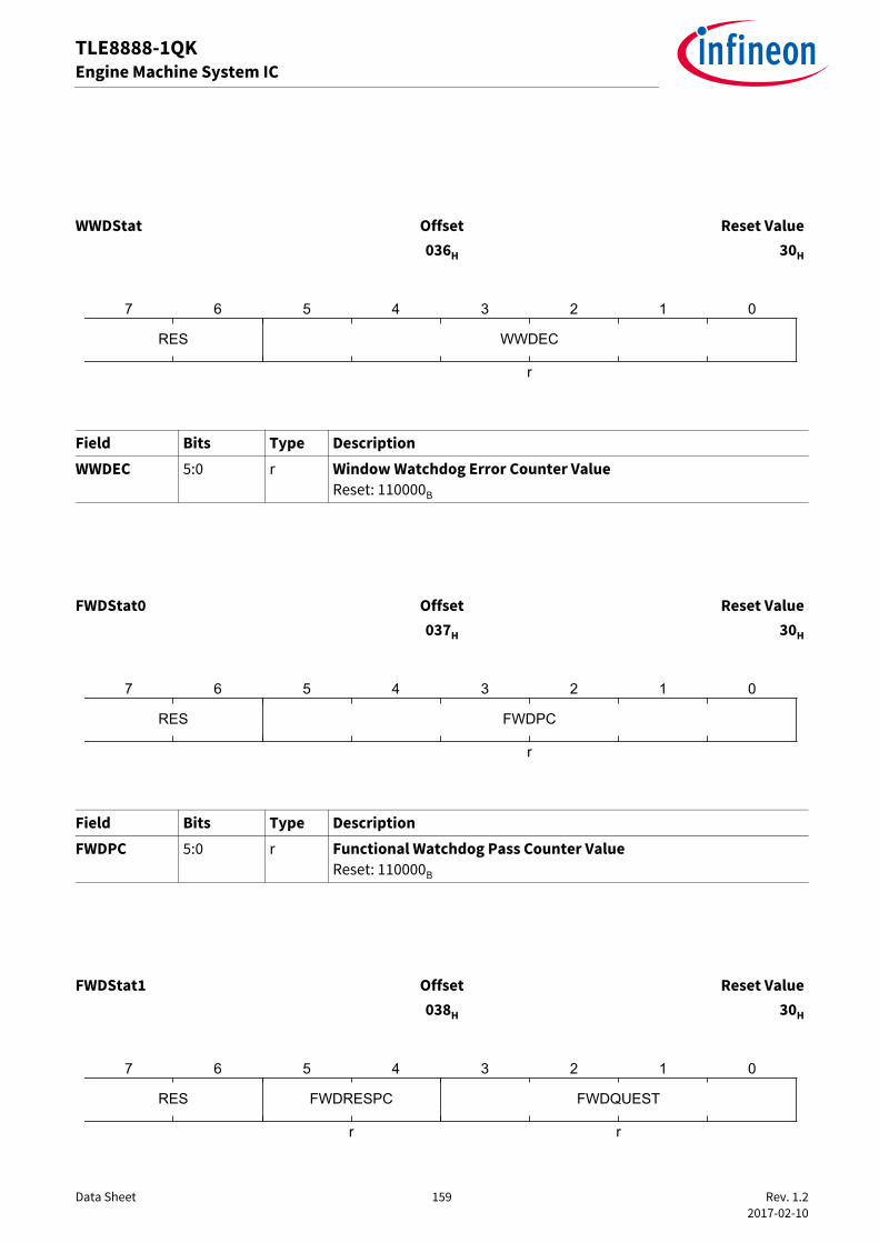
Data Sheet 159 Rev. 1.2 2017-02-10
TLE8888-1QKEngine Machine System IC
WWDStat Offset Reset Value036H 30H
Field Bits Type DescriptionWWDEC 5:0 r Window Watchdog Error Counter Value
Reset: 110000B
FWDStat0 Offset Reset Value037H 30H
Field Bits Type DescriptionFWDPC 5:0 r Functional Watchdog Pass Counter Value
Reset: 110000B
FWDStat1 Offset Reset Value038H 30H
7 6 5 4 3 2 1 0
RES WWDEC
r
7 6 5 4 3 2 1 0
RES FWDPC
r
7 6 5 4 3 2 1 0
RES FWDRESPC
r
FWDQUEST
r

Data Sheet 160 Rev. 1.2 2017-02-10
TLE8888-1QKEngine Machine System IC
Field Bits Type DescriptionFWDRESPC 5:4 r Functional Watchdog Response Counter Value
Reset: 11B
FWDQUEST 3:0 r Functional Watchdog QuestionReset: 0000B
TECStat Offset Reset Value039H 30H
Field Bits Type DescriptionTEC 5:0 r Total Error Counter Value
Reset: 110000B
WdStat0 Offset Reset Value03AH 00H
Field Bits Type DescriptionWWDSCR 7 r Window Watchdog Service Command received
0B , No Service Command received1B , Service Command receivedReset: 0B
SSOTS 6 r Secure Shut Off Timer Start Status Bit:0B , timer reset1B , timer startedReset: 0B
7 6 5 4 3 2 1 0
RES TEC
r
7 6 5 4 3 2 1 0
WWDSCR
r
SSOTS
r
WWDPDC
r
RESC
r

Data Sheet 161 Rev. 1.2 2017-02-10
TLE8888-1QKEngine Machine System IC
WWDPDC 5:3 r Window Watchdog Power-Down Counter ValueReset: 000B
RESC 2:0 r Reset Counter ValueReset: 000B
WdStat1 Offset Reset Value03BH 00H
Field Bits Type DescriptionTECPDC 5:3 r Total Error Power-Down Counter Value
Reset: 000B
FWDPDC 2:0 r Functional Watchdog Power-Down Counter ValueReset: 000B
WDHBT0 Offset Reset Value03CH 00H
Field Bits Type DescriptionWDHBTPRE 3:0 r Sampled Watchdog Heartbeat Timer Predivider Value
Reset: 0000B
Field Bits Type Description
7 6 5 4 3 2 1 0
RES TECPDC
r
FWDPDC
r
7 6 5 4 3 2 1 0
RES WDHBTPRE
r

Data Sheet 162 Rev. 1.2 2017-02-10
TLE8888-1QKEngine Machine System IC
14.1.4 Configuration Register
OutConfig0 locked with LOCK = 1
WDHBT1 Offset Reset Value03DH 00H
Field Bits Type DescriptionWDHBT 6:0 r Sampled Watchdog Heartbeat Timer Value
Reset: 0000000B
OutConfig0 Offset Reset Value040H FFH
Field Bits Type DescriptionO4OL 7 rw Output4 Open Load Set Up:
0B , pull down current deactivated1B , fully functionalReset: 1B
O4OC 6 rw Output4 Overcurrent Protection Set Up:0B , current limitation in case of overcurrent1B , switch off in case of overcurrentReset: 1B
O3OL 5 rw Output3 Open Load Set Up:0B , pull down current deactivated1B , fully functionalReset: 1B
7 6 5 4 3 2 1 0
RES WDHBT
r
7 6 5 4 3 2 1 0
O4OL
rw
O4OC
rw
O3OL
rw
O3OC
rw
O2OL
rw
O2OC
rw
O1OL
rw
O1OC
rw

Data Sheet 163 Rev. 1.2 2017-02-10
TLE8888-1QKEngine Machine System IC
OutConfig1 locked with LOCK = 1
O3OC 4 rw Output3 Overcurrent Protection Set Up:0B , current limitation in case of overcurrent1B , switch off in case of overcurrentReset: 1B
O2OL 3 rw Output2 Open Load Set Up:0B , pull down current deactivated1B , fully functionalReset: 1B
O2OC 2 rw Output2 Overcurrent Protection Set Up:0B , current limitation in case of overcurrent1B , switch off in case of overcurrentReset: 1B
O1OL 1 rw Output1 Open Load Set Up:0B , pull down current deactivated1B , fully functionalReset: 1B
O1OC 0 rw Output1 Overcurrent Protection Set Up:0B , current limitation in case of overcurrent1B , switch off in case of overcurrentReset: 1B
OutConfig1 Offset Reset Value041H 3FH
Field Bits Type DescriptionO7OL 5 rw Output7 Open Load Set Up:
0B , pull down current deactivated1B , fully functionalReset: 1B
O7OC 4 rw Output7 Overcurrent Protection Set Up:0B , current limitation in case of overcurrent1B , switch off in case of overcurrentReset: 1B
Field Bits Type Description
7 6 5 4 3 2 1 0
RES O7OL
rw
O7OC
rw
O6OL
rw
O6OC
rw
O5OL
rw
O5OC
rw

Data Sheet 164 Rev. 1.2 2017-02-10
TLE8888-1QKEngine Machine System IC
OutConfig2 locked with LOCK = 1
O6OL 3 rw Output6 Open Load Set Up:0B , pull down current deactivated1B , fully functionalReset: 1B
O6OC 2 rw Output6 Overcurrent Protection Set Up:0B , current limitation in case of overcurrent1B , switch off in case of overcurrentReset: 1B
O5OL 1 rw Output5 Open Load Set Up:0B , pull down current deactivated1B , fully functionalReset: 1B
O5OC 0 rw Output5 Overcurrent Protection Set Up:0B , current limitation in case of overcurrent1B , switch off in case of overcurrentReset: 1B
OutConfig2 Offset Reset Value042H 3FH
Field Bits Type DescriptionPP0D 7:6 rw Diagnosis in On Set Up for OUT8 and OUT9:
00B , typ. 125 mV short to bat in on threshold01B , typ. 225 mV short to bat in on threshold10B , typ. 400 mV short to bat in on threshold11B , typ. 0.8 V short to bat in on thresholdReset: 00B
O13OL 5 rw Output13 Open Load Set Up:0B , pull down current deactivated1B , fully functionalReset: 1B
O12OL 4 rw Output12 Open Load Set Up:0B , pull down current deactivated1B , fully functionalReset: 1B
Field Bits Type Description
7 6 5 4 3 2 1 0
PP0D
rw
O13OL
rw
O12OL
rw
O11OL
rw
O10OL
rw
O9OL
rw
O8OL
rw

Data Sheet 165 Rev. 1.2 2017-02-10
TLE8888-1QKEngine Machine System IC
OutConfig3 locked with LOCK = 1
O11OL 3 rw Output11 Open Load Set Up:0B , pull down current deactivated1B , fully functionalReset: 1B
O10OL 2 rw Output10 Open Load Set Up:0B , pull down current deactivated1B , fully functionalReset: 1B
O9OL 1 rw Output9 Open Load Set Up:0B , pull down current deactivated1B , fully functionalReset: 1B
O8OL 0 rw Output8 Open Load Set Up:0B , pull down current deactivated1B , fully functionalReset: 1B
OutConfig3 Offset Reset Value043H 30H
Field Bits Type DescriptionO14OL 5 rw Output14 Open Load Set Up:
0B , pull down current deactivated1B , fully functionalReset: 1B
O14OC 4 rw Output14 Overcurrent Protection Set Up:0B , current limitation in case of overcurrent1B , switch off in case of overcurrentReset: 1B
PP2D 3:2 rw Diagnosis in On Set Up for OUT12 and OUT13:00B , typ. 125 mV short to bat in on threshold01B , typ. 225 mV short to bat in on threshold10B , typ. 400 mV short to bat in on threshold11B , typ. 0.8 V short to bat in on thresholdReset: 00B
Field Bits Type Description
7 6 5 4 3 2 1 0
RES O14OL
rw
O14OC
rw
PP2D
rw
PP1D
rw

Data Sheet 166 Rev. 1.2 2017-02-10
TLE8888-1QKEngine Machine System IC
OutConfig4 locked with LOCK = 1
PP1D 1:0 rw Diagnosis in On Set Up for OUT10 and OUT11:00B , typ. 125 mV short to bat in on threshold01B , typ. 225 mV short to bat in on threshold10B , typ. 400 mV short to bat in on threshold11B , typ. 0.8 V short to bat in on thresholdReset: 00B
OutConfig4 Offset Reset Value044H 3FH
Field Bits Type DescriptionO17D 6 rw Output17 Delayed Off Set Up:
0B , no delayed off function1B , delayed off function activatedReset: 0B
O17OL 5 rw Output17 Open Load Set Up:0B , pull down current deactivated1B , fully functionalReset: 1B
O17OC 4 rw Output17 Overcurrent Protection Set Up:0B , current limitation in case of overcurrent1B , switch off in case of overcurrentReset: 1B
O16OL 3 rw Output16 Open Load Set Up:0B , pull down current deactivated1B , fully functionalReset: 1B
O16OC 2 rw Output16 Overcurrent Protection Set Up:0B , current limitation in case of overcurrent1B , switch off in case of overcurrentReset: 1B
O15OL 1 rw Output15 Open Load Set Up:0B , pull down current deactivated1B , fully functionalReset: 1B
Field Bits Type Description
7 6 5 4 3 2 1 0
RES O17D
rw
O17OL
rw
O17OC
rw
O16OL
rw
O16OC
rw
O15OL
rw
O15OC
rw

Data Sheet 167 Rev. 1.2 2017-02-10
TLE8888-1QKEngine Machine System IC
OutConfig5 locked with LOCK = 1
O15OC 0 rw Output15 Overcurrent Protection Set Up:0B , current limitation in case of overcurrent1B , switch off in case of overcurrentReset: 1B
OutConfig5 Offset Reset Value045H 3FH
Field Bits Type DescriptionO20OL 5 rw Output20 Open Load Set Up:
0B , pull down and pull up current deactivated1B , fully functionalReset: 1B
O20OC 4 rw Output20 Overcurrent Protection Set Up:0B , current limitation in case of overcurrent1B , switch off in case of overcurrentReset: 1B
O19OL 3 rw Output19 Open Load Set Up:0B , pull down and pull up current deactivated1B , fully functionalReset: 1B
O19OC 2 rw Output19 Overcurrent Protection Set Up:0B , current limitation in case of overcurrent1B , switch off in case of overcurrentReset: 1B
O18OL 1 rw Output18 Open Load Set Up:0B , pull down and pull up current deactivated1B , fully functionalReset: 1B
O18OC 0 rw Output18 Overcurrent Protection Set Up:0B , current limitation in case of overcurrent1B , switch off in case of overcurrentReset: 1B
Field Bits Type Description
7 6 5 4 3 2 1 0
RES O20OL
rw
O20OC
rw
O19OL
rw
O19OC
rw
O18OL
rw
O18OC
rw

Data Sheet 168 Rev. 1.2 2017-02-10
TLE8888-1QKEngine Machine System IC
BriConfig0 locked with LOCK = 1
BriConfig0 Offset Reset Value046H 00H
Field Bits Type DescriptionO24F 7 rw Output24 Freewheeling Mode Set Up:
0B , passive freewheeling mode1B , active freewheeling modeReset: 0B
O24M 6 rw Output24 Mode Set Up:0B , low-side switch mode1B , high-side switch modeReset: 0B
O23F 5 rw Output23 Freewheeling Mode Set Up:0B , passive freewheeling mode1B , active freewheeling modeReset: 0B
O23M 4 rw Output23 Mode Set Up:0B , low-side switch mode1B , high-side switch modeReset: 0B
O22F 3 rw Output22 Freewheeling Mode Set Up:0B , passive freewheeling mode1B , active freewheeling modeReset: 0B
O22M 2 rw Output22 Mode Set Up:0B , low-side switch mode1B , high-side switch modeReset: 0B
O21F 1 rw Output21 Freewheeling Mode Set Up:0B , passive freewheeling mode1B , active freewheeling modeReset: 0B
O21M 0 rw Output21 Mode Set Up:0B , low-side switch mode1B , high-side switch modeReset: 0B
7 6 5 4 3 2 1 0
O24F
rw
O24M
rw
O23F
rw
O23M
rw
O22F
rw
O22M
rw
O21F
rw
O21M
rw

Data Sheet 169 Rev. 1.2 2017-02-10
TLE8888-1QKEngine Machine System IC
BriConfig1 locked with LOCK = 1
IGNConfig locked with LOCK = 1
BriConfig1 Offset Reset Value047H 00H
Field Bits Type DescriptionFB2E 2 rw Full Bridge 2 Enable Bit:
0B , Output 23 and 24 are not used in full bridge configuration1B , Output 23 and 24 are used in full bridge configurationReset: 0B
FB1E 1 rw Full Bridge 1 Enable Bit:0B , Output 21 and 22 are not used in full bridge configuration1B , Output 21 and 22 are used in full bridge configurationReset: 0B
O21D 0 rw Output21 Delayed Off Set Up:0B , no delayed off function1B , delayed off function activatedReset: 0B
IGNConfig Offset Reset Value048H 00H
7 6 5 4 3 2 1 0
RES FB2E
rw
FB1E
rw
O21D
rw
7 6 5 4 3 2 1 0
RES IOLT
rw
IOLI
rw
IOLA
rw

Data Sheet 170 Rev. 1.2 2017-02-10
TLE8888-1QKEngine Machine System IC
Field Bits Type DescriptionIOLT 4:3 rw Ignition Time Setting for Open Load Detection:
00B , 64 μs01B , 256 μs10B , 512 μs11B , 768 μsReset: 00B
IOLI 2:1 rw Ignition Current Setting for Open Load Detection:00B , -100 μA01B , -400 μA10B , -1 mA11B , -4 mAReset: 00B
IOLA 0 rw Ignition Open Load Detection Activation:0B , no open load detection1B , open load detection activeReset: 0B
VRSConfig0 Offset Reset Value049H 00H
Field Bits Type DescriptionVRSPV 7:6 rw VRS Peak Voltage Detection Set Up:
00B , 50 mV01B , 150 mV10B , 350 mV11B , 550 mVReset: 00B
VRSF 2:1 rw VRS Output Filter Time Set Up:00B , 1 μs, reset value01B , 5 μs10B , 10 μs11B , 20 μsReset: 00B
7 6 5 4 3 2 1 0
VRSPV
rw
RES VRSF
rw
VRSPT
rw
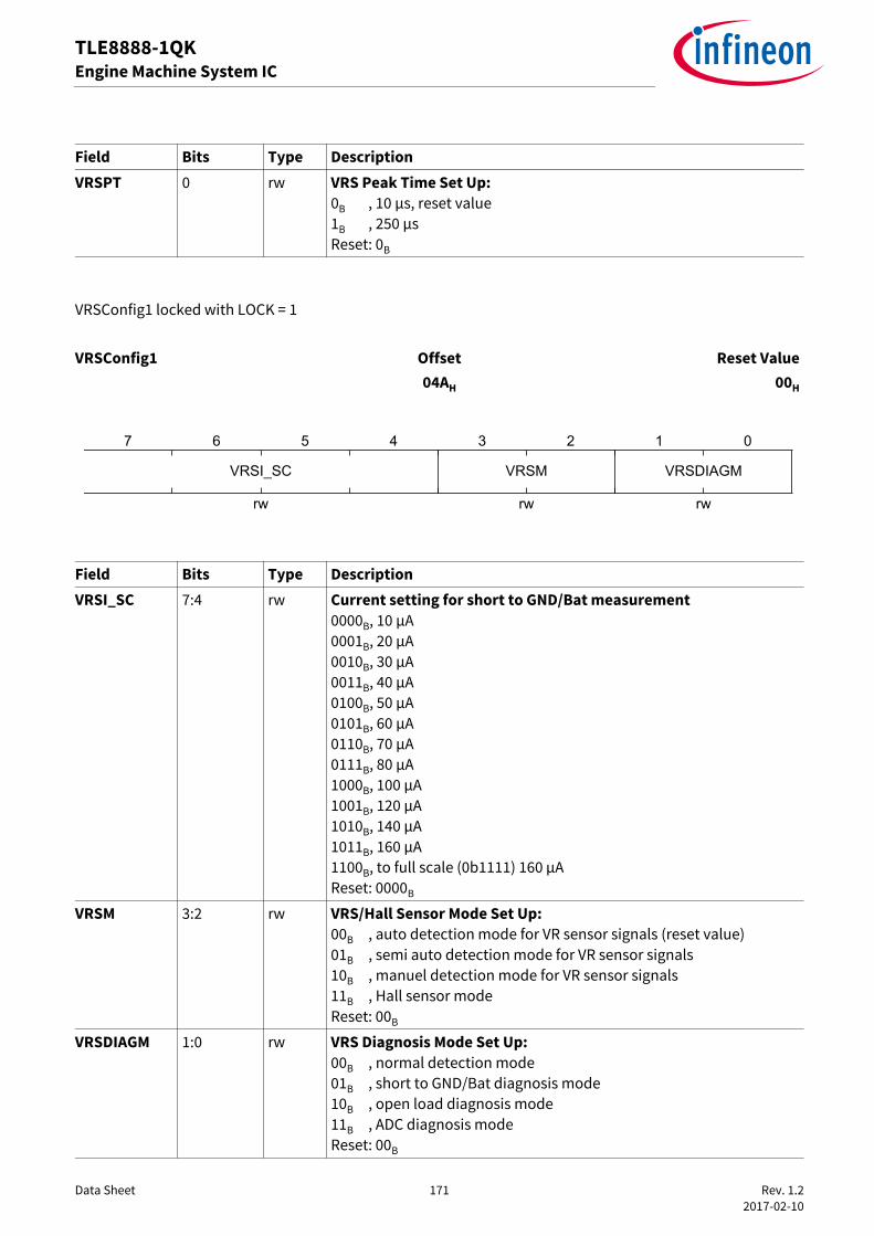
Data Sheet 171 Rev. 1.2 2017-02-10
TLE8888-1QKEngine Machine System IC
VRSConfig1 locked with LOCK = 1
VRSPT 0 rw VRS Peak Time Set Up:0B , 10 μs, reset value1B , 250 μsReset: 0B
VRSConfig1 Offset Reset Value04AH 00H
Field Bits Type DescriptionVRSI_SC 7:4 rw Current setting for short to GND/Bat measurement
0000B, 10 μA0001B, 20 μA0010B, 30 μA0011B, 40 μA0100B, 50 μA0101B, 60 μA0110B, 70 μA0111B, 80 μA1000B, 100 μA1001B, 120 μA1010B, 140 μA1011B, 160 μA1100B, to full scale (0b1111) 160 μAReset: 0000B
VRSM 3:2 rw VRS/Hall Sensor Mode Set Up:00B , auto detection mode for VR sensor signals (reset value)01B , semi auto detection mode for VR sensor signals10B , manuel detection mode for VR sensor signals11B , Hall sensor modeReset: 00B
VRSDIAGM 1:0 rw VRS Diagnosis Mode Set Up:00B , normal detection mode01B , short to GND/Bat diagnosis mode10B , open load diagnosis mode11B , ADC diagnosis modeReset: 00B
Field Bits Type Description
7 6 5 4 3 2 1 0
VRSI_SC
rw
VRSM
rw
VRSDIAGM
rw

Data Sheet 172 Rev. 1.2 2017-02-10
TLE8888-1QKEngine Machine System IC
VRSConfig2 locked with LOCK = 1
OpConfig0 locked with LOCK = 1
VRSConfig2 Offset Reset Value04BH 00H
Field Bits Type DescriptionVRSI_ADC 7:4 rw Current setting for ADC measurement
0000B, 10 μA0001B, 20 μA0010B, 30 μA0011B, 40 μA0100B, 50 μA0101B, 60 μA0110B, 70 μA0111B, 80 μA1000B, 100 μA1001B, 120 μA1010B, 140 μA1011B, 160 μA1100B, to full scale (0b1111) 160 μAReset: 0000B
VRSI_OL 3:0 rw Current setting for open load measurement0000B, 10 μA0001B, 20 μA0010B, 30 μA0011B, 40 μA0100B, 50 μA0101B, 60 μA0110B, 70 μA0111B, 80 μA1000B, 100 μA1001B, 120 μA1010B, 140 μA1011B, 160 μA1100B, to full scale (0b1111) 160 μAReset: 0000B
7 6 5 4 3 2 1 0
VRSI_ADC
rw
VRSI_OL
rw

Data Sheet 173 Rev. 1.2 2017-02-10
TLE8888-1QKEngine Machine System IC
ComConfig0 locked with LOCK = 1
OpConfig0 Offset Reset Value04EH 09H
Field Bits Type DescriptionKOD 6:5 rw Key Off Delay Set Up:
00B , 100 ms01B , 200 ms10B , 400 ms11B , 800 msReset: 00B
EOTCONF 4 rw Engine Off Timer Configuration:0B , timer start with negative edge of KEY signal1B , timer start with command EOTS in register Cmd0Reset: 0B
AR 3 rw Afterrun Reset Behavior Set Up:0B , no afterrun reset1B , afterrun resetReset: 1B
AE 2 rw Afterrun Enable:0B , no afterrun mode1B , afterrun modeReset: 0B
PDT 1:0 rw Power-Down Time Set Up:00B , 100 ms01B , 200 ms10B , 300 ms11B , 400 msReset: 01B
ComConfig0 Offset Reset Value04FH A4H
7 6 5 4 3 2 1 0
RES KOD
rw
EOTCONF
rw
AR
rw
AE
rw
PDT
rw

Data Sheet 174 Rev. 1.2 2017-02-10
TLE8888-1QKEngine Machine System IC
ComConfig1 locked with LOCK = 1
Field Bits Type DescriptionMSCF 7:5 rw MSC Upstream Frequency Divider Set Up:
000B , Division by 64001B , Division by 4010B , Division by 8011B , Division by 16100B , Division by 32101B , Division by 64110B , Division by 128111B , Division by 256Reset: 101B
MSCO 4 rw MSC SDO Definition:0B , open drain1B , push pullReset: 0B
MSCAD 3 rw MSC Address Definition A0 to A3:0B , value of A2 to A3 are incremented with each read command1B , A0 to A3 values are fixed to the values of MSCA[3:0]Reset: 0B
MSCP 2 rw MSC Upstream Parity Format Set Up:0B , odd parity1B , even parityReset: 1B
MSCUF 1:0 rw MSC Upstream Address Format Setup:00B , upstream format without address01B , upstream format with address10B , upstream format with address11B , upstream format with addressReset: 00B
ComConfig1 Offset Reset Value050H 0DH
7 6 5 4 3 2 1 0
MSCF
rw
MSCO
rw
MSCAD
rw
MSCP
rw
MSCUF
rw

Data Sheet 175 Rev. 1.2 2017-02-10
TLE8888-1QKEngine Machine System IC
EOTConfig0 locked with LOCK = 1
EOTConfig1 locked with LOCK = 1
Field Bits Type DescriptionMSCA 7:4 rw MSC Upstream Address for MSCAD = 1
Reset: 0000B
LINTOE 3 rw LIN TX Time OUT Function Enable:0B , TX time out function disabled1B , TX time out function enabledReset: 1B
LIN 2:1 rw Operation Mode:00B , receive only mode01B , LIN/K-line operation10B , flash mode11B , receive only modeReset: 10B
CAN 0 rw CAN Operation Mode:0B , receive only mode1B , high speed CAN modeReset: 1B
EOTConfig0 Offset Reset Value051H 00H
Field Bits Type DescriptionEOTTH0 7:0 rw Engine Off Timer Comparator Threshold: (Bit 7 - 0)
Reset: 00H
7 6 5 4 3 2 1 0
MSCA
rw
LINTOE
rw
LIN
rw
CAN
rw
7 6 5 4 3 2 1 0
EOTTH0
rw
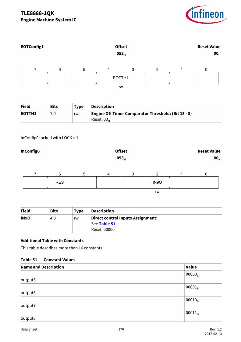
Data Sheet 176 Rev. 1.2 2017-02-10
TLE8888-1QKEngine Machine System IC
InConfig0 locked with LOCK = 1
Additional Table with ConstantsThis table describes more than 16 constants.
EOTConfig1 Offset Reset Value052H 00H
Field Bits Type DescriptionEOTTH1 7:0 rw Engine Off Timer Comparator Threshold: (Bit 15 - 8)
Reset: 00H
InConfig0 Offset Reset Value053H 00H
Field Bits Type DescriptionIN9O 4:0 rw Direct control Input9 Assignment:
See Table 51Reset: 00000B
Table 51 Constant ValuesName and Description Value
output500000B
output600001B
output700010B
output800011B
7 6 5 4 3 2 1 0
EOTTH1
rw
7 6 5 4 3 2 1 0
RES IN9O
rw

Data Sheet 177 Rev. 1.2 2017-02-10
TLE8888-1QKEngine Machine System IC
InConfig1 locked with LOCK = 1
output900100B
output1000101B
output1100110B
output1200111B
output1301000B
output1401001B
output1501010B
output1601011B
output1701100B
output1801101B
output1901110B
output2001111B
output2110000B
output2210001B
output2310010B
output2410011B
InConfig1 Offset Reset Value054H 00H
Table 51 Constant Values (cont’d)Name and Description Value

Data Sheet 178 Rev. 1.2 2017-02-10
TLE8888-1QKEngine Machine System IC
Additional Table with ConstantsThis table describes more than 16 constants.
Field Bits Type DescriptionIN10O 4:0 rw Direct control Input10 Assignment:
See Table 52Reset: 00000B
Table 52 Constant ValuesName and Description Value
output500000B
output600001B
output700010B
output800011B
output900100B
output1000101B
output1100110B
output1200111B
output1301000B
output1401001B
output1501010B
output1601011B
output1701100B
output1801101B
7 6 5 4 3 2 1 0
RES IN10O
rw

Data Sheet 179 Rev. 1.2 2017-02-10
TLE8888-1QKEngine Machine System IC
InConfig2 locked with LOCK = 1
Additional Table with ConstantsThis table describes more than 16 constants.
output1901110B
output2001111B
output2110000B
output2210001B
output2310010B
output2410011B
InConfig2 Offset Reset Value055H 00H
Field Bits Type DescriptionIN11O 4:0 rw Direct control Input11 Assignment:
See Table 53Reset: 00000B
Table 53 Constant ValuesName and Description Value
output500000B
output600001B
output700010B
Table 52 Constant Values (cont’d)Name and Description Value
7 6 5 4 3 2 1 0
RES IN11O
rw

Data Sheet 180 Rev. 1.2 2017-02-10
TLE8888-1QKEngine Machine System IC
InConfig3 locked with LOCK = 1
output800011B
output900100B
output1000101B
output1100110B
output1200111B
output1301000B
output1401001B
output1501010B
output1601011B
output1701100B
output1801101B
output1901110B
output2001111B
output2110000B
output2210001B
output2310010B
output2410011B
InConfig3 Offset Reset Value056H 00H
Table 53 Constant Values (cont’d)Name and Description Value

Data Sheet 181 Rev. 1.2 2017-02-10
TLE8888-1QKEngine Machine System IC
Additional Table with ConstantsThis table describes more than 16 constants.
Field Bits Type DescriptionIN12O 4:0 rw Direct control Input12 Assignment:
See Table 54Reset: 00000B
Table 54 Constant ValuesName and Description Value
output500000B
output600001B
output700010B
output800011B
output900100B
output1000101B
output1100110B
output1200111B
output1301000B
output1401001B
output1501010B
output1601011B
output1701100B
output1801101B
7 6 5 4 3 2 1 0
RES IN12O
rw

Data Sheet 182 Rev. 1.2 2017-02-10
TLE8888-1QKEngine Machine System IC
DDConfig0 locked with LOCK = 1
output1901110B
output2001111B
output2110000B
output2210001B
output2310010B
output2410011B
DDConfig0 Offset Reset Value057H 00H
Field Bits Type DescriptionO8DD 7 rw Output8 Direct Drive Control: see below
Reset: 0B
O7DD 6 rw Output7 Direct Drive Control: see belowReset: 0B
O6DD 5 rw Output6 Direct Drive Control: see belowReset: 0B
O5DD 4 rw Output5 Direct Drive Control: see belowReset: 0B
O4DD 3 rw Output4 Direct Drive Control: see belowReset: 0B
O3DD 2 rw Output3 Direct Drive Control: see belowReset: 0B
O2DD 1 rw Output2 Direct Drive Control: see belowReset: 0B
Table 54 Constant Values (cont’d)Name and Description Value
7 6 5 4 3 2 1 0
O8DD
rw
O7DD
rw
O6DD
rw
O5DD
rw
O4DD
rw
O3DD
rw
O2DD
rw
O1DD
rw

Data Sheet 183 Rev. 1.2 2017-02-10
TLE8888-1QKEngine Machine System IC
DDConfig1 locked with LOCK = 1
DDConfig2 locked with LOCK = 1
O1DD 0 rw Output1 Direct Drive Control:0B , controlled by MSC/SPI interface1B , controlled by Direct Drive InputReset: 0B
DDConfig1 Offset Reset Value058H 00H
Field Bits Type DescriptionO16DD 7 rw Output16 Direct Drive Control: see below
Reset: 0B
O15DD 6 rw Output15 Direct Drive Control: see belowReset: 0B
O14DD 5 rw Output14 Direct Drive Control: see belowReset: 0B
O13DD 4 rw Output13 Direct Drive Control: see belowReset: 0B
O12DD 3 rw Output12 Direct Drive Control: see belowReset: 0B
O11DD 2 rw Output11 Direct Drive Control: see belowReset: 0B
O10DD 1 rw Output10 Direct Drive Control: see belowReset: 0B
O9DD 0 rw Output9 Direct Drive Control:0B , controlled by MSC/SPI interface1B , controlled by Direct Drive InputReset: 0B
DDConfig2 Offset Reset Value059H 00H
Field Bits Type Description
7 6 5 4 3 2 1 0
O16DD
rw
O15DD
rw
O14DD
rw
O13DD
rw
O12DD
rw
O11DD
rw
O10DD
rw
O9DD
rw

Data Sheet 184 Rev. 1.2 2017-02-10
TLE8888-1QKEngine Machine System IC
DDConfig3 locked with LOCK = 1
Field Bits Type DescriptionO24DD 7 rw Output24 Direct Drive Control: see below
Reset: 0B
O23DD 6 rw Output23 Direct Drive Control: see belowReset: 0B
O22DD 5 rw Output22 Direct Drive Control: see belowReset: 0B
O21DD 4 rw Output21 Direct Drive Control: see belowReset: 0B
O20DD 3 rw Output20 Direct Drive Control: see belowReset: 0B
O19DD 2 rw Output19 Direct Drive Control: see belowReset: 0B
O18DD 1 rw Output18 Direct Drive Control: see belowReset: 0B
O17DD 0 rw Output17 Direct Drive Control:0B , controlled by MSC/SPI interface1B , controlled by Direct Drive InputReset: 0B
DDConfig3 Offset Reset Value05AH 00H
Field Bits Type DescriptionIGN4DD 3 rw Ignition Output4 Direct Drive Control: see below
Reset: 0B
IGN3DD 2 rw Ignition Output3 Direct Drive Control: see belowReset: 0B
7 6 5 4 3 2 1 0
O24DD
rw
O23DD
rw
O22DD
rw
O21DD
rw
O20DD
rw
O19DD
rw
O18DD
rw
O17DD
rw
7 6 5 4 3 2 1 0
RES IGN4DD
rw
IGN3DD
rw
IGN2DD
rw
IGN1DD
rw

Data Sheet 185 Rev. 1.2 2017-02-10
TLE8888-1QKEngine Machine System IC
IGN2DD 1 rw Ignition Output2 Direct Drive Control: see belowReset: 0B
IGN1DD 0 rw Ignition Output1 Direct Drive Control:0B , controlled by MSC/SPI interface1B , controlled by Direct Drive InputReset: 0B
OEConfig0 Offset Reset Value05BH 00H
Field Bits Type DescriptionO8E 7 rw Output8 Enable Bit:
0B , output disabled1B , output enabledReset: 0B
O7E 6 rw Output7 Enable Bit:0B , output disabled1B , output enabledReset: 0B
O6E 5 rw Output6 Enable Bit:0B , output disabled1B , output enabledReset: 0B
O5E 4 rw Output5 Enable Bit:0B , output disabled1B , output enabledReset: 0B
O4E 3 rw Output4 Enable Bit:0B , output disabled1B , output enabledReset: 0B
O3E 2 rw Output3 Enable Bit:0B , output disabled1B , output enabledReset: 0B
Field Bits Type Description
7 6 5 4 3 2 1 0
O8E
rw
O7E
rw
O6E
rw
O5E
rw
O4E
rw
O3E
rw
O2E
rw
O1E
rw

Data Sheet 186 Rev. 1.2 2017-02-10
TLE8888-1QKEngine Machine System IC
O2E 1 rw Output2 Enable Bit:0B , output disabled1B , output enabledReset: 0B
O1E 0 rw Output1 Enable Bit:0B , output disabled1B , output enabledReset: 0B
OEConfig1 Offset Reset Value05CH 00H
Field Bits Type DescriptionO16E 7 rw Output16 Enable Bit:
0B , output disabled1B , output enabledReset: 0B
O15E 6 rw Output15 Enable Bit:0B , output disabled1B , output enabledReset: 0B
O14E 5 rw Output14 Enable Bit:0B , output disabled1B , output enabledReset: 0B
O13E 4 rw Output13 Enable Bit:0B , output disabled1B , output enabledReset: 0B
O12E 3 rw Output12 Enable Bit:0B , output disabled1B , output enabledReset: 0B
Field Bits Type Description
7 6 5 4 3 2 1 0
O16E
rw
O15E
rw
O14E
rw
O13E
rw
O12E
rw
O11E
rw
O10E
rw
O9E
rw

Data Sheet 187 Rev. 1.2 2017-02-10
TLE8888-1QKEngine Machine System IC
O11E 2 rw Output11 Enable Bit:0B , output disabled1B , output enabledReset: 0B
O10E 1 rw Output10 Enable Bit:0B , output disabled1B , output enabledReset: 0B
O9E 0 rw Output9 Enable Bit:0B , output disabled1B , output enabledReset: 0B
OEConfig2 Offset Reset Value05DH 00H
Field Bits Type DescriptionO24E 7 rw Output24 Enable Bit:
0B , output disabled1B , output enabledReset: 0B
O23E 6 rw Output23 Enable Bit:0B , output disabled1B , output enabledReset: 0B
O22E 5 rw Output22 Enable Bit:0B , output disabled1B , output enabledReset: 0B
O21E 4 rw Output21 Enable Bit:0B , output disabled1B , output enabledReset: 0B
Field Bits Type Description
7 6 5 4 3 2 1 0
O24E
rw
O23E
rw
O22E
rw
O21E
rw
O20E
rw
O19E
rw
O18E
rw
O17E
rw

Data Sheet 188 Rev. 1.2 2017-02-10
TLE8888-1QKEngine Machine System IC
O20E 3 rw Output20 Enable Bit:0B , output disabled1B , output enabledReset: 0B
O19E 2 rw Output19 Enable Bit:0B , output disabled1B , output enabledReset: 0B
O18E 1 rw Output18 Enable Bit:0B , output disabled1B , output enabledReset: 0B
O17E 0 rw Output17 Enable Bit:0B , output disabled1B , output enabledReset: 0B
OEConfig3 Offset Reset Value05EH 00H
Field Bits Type DescriptionIGN4E 3 rw Ignition 4 Output Enable Bit:
0B , output disabled1B , output enabledReset: 0B
IGN3E 2 rw Ignition 3 Output Enable Bit:0B , output disabled1B , output enabledReset: 0B
IGN2E 1 rw Ignition 2 Output Enable Bit:0B , output disabled1B , output enabledReset: 0B
Field Bits Type Description
7 6 5 4 3 2 1 0
RES IGN4E
rw
IGN3E
rw
IGN2E
rw
IGN1E
rw

Data Sheet 189 Rev. 1.2 2017-02-10
TLE8888-1QKEngine Machine System IC
IGN1E 0 rw Ignition 1 Output Enable Bit:0B , output disabled1B , output enabledReset: 0B
WWDConfig0 Offset Reset Value05FH FFH
Field Bits Type DescriptionWWDCWT 7:2 rw Window Watchdog Closed Window Time:
000000B, no change - old setting used for open and closed window000001B, 1,6 ms111111B, 100,8 msReset: 111111B
WWDOWT 1:0 rw Window Watchdog Open Window Time:00B , 3,2 ms01B , 6,4 ms10B , 9,6 ms11B , 12,8 msReset: 11B
WWDConfig1 Offset Reset Value060H 77H
Field Bits Type Description
7 6 5 4 3 2 1 0
WWDCWT
rw
WWDOWT
rw
7 6 5 4 3 2 1 0
WWDECD
rw
WWDECI
rw

Data Sheet 190 Rev. 1.2 2017-02-10
TLE8888-1QKEngine Machine System IC
Field Bits Type DescriptionWWDECD 7:4 rw Window Watchdog Error Counter Decrement:
0000B, -10001B, -21111B, -16Reset: 0111B
WWDECI 3:0 rw Window Watchdog Error Counter Increment:0000B, +10001B, +21111B, +16Reset: 0111B
FWDConfig Offset Reset Value061H F7H
Field Bits Type DescriptionFWDPCD 7:4 rw Functional Watchdog Pass Counter Decrement:
0000B, -10001B, -21111B, -16Reset: 1111B
FWDPCI 3:0 rw Functional Watchdog Pass Counter Increment:0000B, +10001B, +21111B, +16Reset: 0111B
TECConfig Offset Reset Value062H 77H
7 6 5 4 3 2 1 0
FWDPCD
rw
FWDPCI
rw
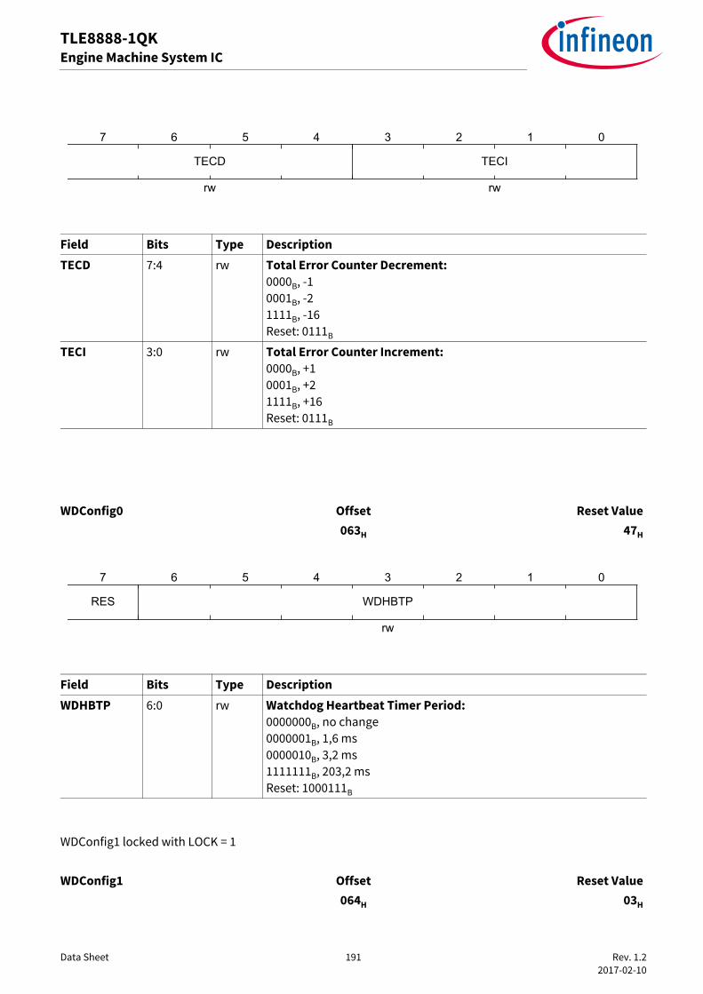
Data Sheet 191 Rev. 1.2 2017-02-10
TLE8888-1QKEngine Machine System IC
WDConfig1 locked with LOCK = 1
Field Bits Type DescriptionTECD 7:4 rw Total Error Counter Decrement:
0000B, -10001B, -21111B, -16Reset: 0111B
TECI 3:0 rw Total Error Counter Increment:0000B, +10001B, +21111B, +16Reset: 0111B
WDConfig0 Offset Reset Value063H 47H
Field Bits Type DescriptionWDHBTP 6:0 rw Watchdog Heartbeat Timer Period:
0000000B, no change0000001B, 1,6 ms0000010B, 3,2 ms1111111B, 203,2 msReset: 1000111B
WDConfig1 Offset Reset Value064H 03H
7 6 5 4 3 2 1 0
TECD
rw
TECI
rw
7 6 5 4 3 2 1 0
RES WDHBTP
rw

Data Sheet 192 Rev. 1.2 2017-02-10
TLE8888-1QKEngine Machine System IC
14.1.5 Control Register
Field Bits Type DescriptionFWDKQ 4 rw Functional Watchdog Keep Question Setup:
0B , No influence to question generation in case of window watchdog error
1B , Keep question in case of window watchdog errorReset: 0B
FWDQG 3 rw Functional Watchdog Question Generation:0B , Question period 161B , Question period 256Reset: 0B
WDREN 2 rw Watchdog Reset Enable Bit:0B , reset disabled1B , reset enabledReset: 0B
LINWE 1 rw LIN Operation Mode during Watchdog Error Setup:0B , receive only mode1B , according ComConfig1.LINReset: 1B
CANWE 0 rw CAN Operation Mode during Watchdog Error Setup:0B , receive only mode1B , according ComConfig1.CANReset: 1B
Cont0 Offset Reset Value07BH 00H
7 6 5 4 3 2 1 0
RES FWDKQ
rw
FWDQG
rw
WDREN
rw
LINWE
rw
CANWE
rw
7 6 5 4 3 2 1 0
O8ON
rw
O7ON
rw
O6ON
rw
O5ON
rw
O4ON
rw
O3ON
rw
O2ON
rw
O1ON
rw

Data Sheet 193 Rev. 1.2 2017-02-10
TLE8888-1QKEngine Machine System IC
Field Bits Type DescriptionO8ON 7 rw Output8 Switch on Control Bit:
0B , off1B , onReset: 0B
O7ON 6 rw Output7 Switch on Control Bit:0B , off1B , onReset: 0B
O6ON 5 rw Output6 Switch on Control Bit:0B , off1B , onReset: 0B
O5ON 4 rw Output5 Switch on Control Bit:0B , off1B , onReset: 0B
O4ON 3 rw Output4 Switch on Control Bit:0B , off1B , onReset: 0B
O3ON 2 rw Output3 Switch on Control Bit:0B , off1B , onReset: 0B
O2ON 1 rw Output2 Switch on Control Bit:0B , off1B , onReset: 0B
O1ON 0 rw Output1 Switch on Control Bit:0B , off1B , onReset: 0B
Cont1 Offset Reset Value07CH 00H
7 6 5 4 3 2 1 0
O16ON
rw
O15ON
rw
O14ON
rw
O13ON
rw
O12ON
rw
O11ON
rw
O10ON
rw
O9ON
rw

Data Sheet 194 Rev. 1.2 2017-02-10
TLE8888-1QKEngine Machine System IC
Field Bits Type DescriptionO16ON 7 rw Output16 Switch on Control Bit:
0B , off1B , onReset: 0B
O15ON 6 rw Output15 Switch on Control Bit:0B , off1B , onReset: 0B
O14ON 5 rw Output14 Switch on Control Bit:0B , off1B , onReset: 0B
O13ON 4 rw Output13 Switch on Control Bit:0B , off1B , onReset: 0B
O12ON 3 rw Output12 Switch on Control Bit:0B , off1B , onReset: 0B
O11ON 2 rw Output11 Switch on Control Bit:0B , off1B , onReset: 0B
O10ON 1 rw Output10 Switch on Control Bit:0B , off1B , onReset: 0B
O9ON 0 rw Output9 Switch on Control Bit:0B , off1B , onReset: 0B
Cont2 Offset Reset Value07DH 00H
7 6 5 4 3 2 1 0
O24ON
rw
O23ON
rw
O22ON
rw
O21ON
rw
O20ON
rw
O19ON
rw
O18ON
rw
O17ON
rw

Data Sheet 195 Rev. 1.2 2017-02-10
TLE8888-1QKEngine Machine System IC
Field Bits Type DescriptionO24ON 7 rw Output24 Switch on Control Bit:
0B , off1B , onReset: 0B
O23ON 6 rw Output23 Switch on Control Bit:0B , off1B , onReset: 0B
O22ON 5 rw Output22 Switch on Control Bit:0B , off1B , onReset: 0B
O21ON 4 rw Output21 Switch on Control Bit:0B , off1B , onReset: 0B
O20ON 3 rw Output20 Switch on Control Bit:0B , off1B , onReset: 0B
O19ON 2 rw Output19 Switch on Control Bit:0B , off1B , onReset: 0B
O18ON 1 rw Output18 Switch on Control Bit:0B , off1B , onReset: 0B
O17ON 0 rw Output17 Switch on Control Bit:0B , off1B , onReset: 0B
Cont3 Offset Reset Value07EH 00H
7 6 5 4 3 2 1 0
RES IGN4ON
rw
IGN3ON
rw
IGN2ON
rw
IGN1ON
rw

Data Sheet 196 Rev. 1.2 2017-02-10
TLE8888-1QKEngine Machine System IC
Field Bits Type DescriptionIGN4ON 3 rw Ignition Output4 Switch on Control Bit:
0B , off1B , onReset: 0B
IGN3ON 2 rw Ignition Output3 Switch on Control Bit:0B , off1B , onReset: 0B
IGN2ON 1 rw Ignition Output2 Switch on Control Bit:0B , off1B , onReset: 0B
IGN1ON 0 rw Ignition Output1 Switch on Control Bit:0B , off1B , onReset: 0B

Data Sheet 197 Rev. 1.2 2017-02-10
TLE8888-1QKEngine Machine System IC
SPI
15 SPIAlternatively to the MSC communication interface a SPI interface is available. It uses the pins SIP, SDO, CSNand FCLP. The configuration is done via the pins FCLN and SIN. FCLN must be connected to VDDIO andSIN must be connected to AGND. In SPI mode the output stage of the pin SDO is set to push pull operation(definition and description see Chapter 13.2 and Chapter 13.4).The definition of the registers is the same as for the MSC communication (see Chapter 14), only the frame isSPI specific (see Figure 67 and Chapter 15.1). Multiple read commands are not allowed.There is no monitoring of valid transmissions implemented (like MSC monitoring, see Chapter 13.1.1).
Figure 66 Block diagram of the SPI interface
15.1 SPI ProtocolThe principle of the SPI communication is shown in Figure 67. The message from the microcontroller must besent LSB first. The data from the SDO pin is sent LSB first. The TLE8888-1QK samples data from the SIP pinon the falling edge of FCLP and shifts data out of the SDO pin on the rising edge of FCLP. Each access mustbe terminated by a rising edge of CSN.
All SPI messages must be exactly 16 bits long, otherwise the SPI message is discarded and the bit COMFE indiagnosis register ComDiag is set to “1”.
There is one message delay in the response to each message (i.e. the response for message N will be returnedduring message N+1).
There are two valid access possible:• Write access to registers with write permission: the answer is 1 for the R/W bit, the address and the content
of the register• Read access to register with read permission: the answer is 0 for the R/W bit, the address and the content
of the registerEverything else is not executed. Write access to multiple read commands are also not valid in SPI mode.
MSC
SPI
+-
+-+-REF
SDO
FCLN
SIP
SIN
CSN
FCLP
VDDIO

Data Sheet 198 Rev. 1.2 2017-02-10
TLE8888-1QKEngine Machine System IC
SPI
Status Flag Indication: after the falling edge of CSN and before the first rising edge of FCLP the level of theSDO indicates an OR combination of the status of the central failure bit CF and the central overtemperaturebit COT of the diagnosis register Diag0.With this feature during every SPI communication a check of the diagnosis status can be done withoutadditional read access of the diagnosis register.
Figure 67 SPI Protocol
SPI Answers:• during power on reset: SPI commands are ignored, SDO is always tristate• after power on reset: the address and the content of the status register OpStat0 is transmitted with the
next SPI transmission• during watchdog reset: SPI commands are ignored, SDO has the value of the status flag• after watchdog reset: the address and the content of the diagnosis register FWDStat1 is transmitted with
the first SPI transmission after the low to high transition of RST• after a read or write command: the address and content of the selected register is transmitted with the
next SPI transmission (for not existing addresses or wrong access mode the data is always “0”)• after an invalid communication frame: the address and the content of the diagnosis register Diag0 is
transmitted with the next SPI transmission and the bit COMFE in diagnosis register ComDiag is set to “1”
Bit 0LSB
Bit 15MSB
don’t care don’t care
clock1
clock2
clock3
clock15
clock16
Bit 1 Bit 2 Bit 14
don’t care
Bit 15MSB
Bit 0LSB Bit 1
tristatetristate
time
time
time
time
don’t care
Bit 15Bit 2
FCLP
SIP
SDO
CSN
Status Flag
* )
*) active clock edge for reading data at SI

Data Sheet 199 Rev. 1.2 2017-02-10
TLE8888-1QKEngine Machine System IC
SPI
15.2 SPI Frame Definition
Overview SPI Frame
15 14 13 12 11 10 9 8 7 6 5 4 3 2 1 0
CD7 CD6 CD5 CD4 CD3 CD2 CD1 CD0 C7 C6 C5 C4 C3 C2 C1 C0
Field Bits Type DescriptionC0 0 R/W Bit: defines the access to the registerC[7:1] [7:1] Address Bits, definition see Chapter 14CD[7:0] [15:8] Data Bits, definition see Chapter 14
Data Sheet 200 Rev. 1.2 2017-02-10
TLE8888-1QKEngine Machine System IC
SPI
15.3 Electrical Characteristics SPI
Table 55 Electrical Characteristics CommunicationVS = 13.5 V, VVSV = 5 V, Tj = -40°C to +150°C, all voltages with respect to GND, positive current flowing into pin,(unless otherwise specified)
Parameter Symbol Values Unit Note or Test Condition
NumberMin. Typ. Max.
SPI detection threshold for SIN
VFCLN_SPI 0.3 – 0.7 V P_15.1
Single ended mode detection threshold for FCLN
VFCLN_single
2 – 3 V P_15.2
SDO see Chapter 13.4 P_15.3
Input low level (SIP, FCLP, CSN)
VINn_L -0.3 – 0.8 V P_15.4
Input high level (SIP, FCLP, CSN)
VINn_H 1.6 – 5.5 V P_15.5
Input hysteresis (SIP, FCLP, CSN)
VINn_Hys 0.1 – 0.5 V P_15.6
Clock frequency fSPI – – 5 MHz P_15.7

Data Sheet 201 Rev. 1.2 2017-02-10
TLE8888-1QKEngine Machine System IC
EMC Requirements
16 EMC Requirements
16.1 ISO Pulse TestsDefinitions for all ISO pulse test on application including the TLE8888-1QK are regarding standard ISO 7637-2:2011. The following amplitude definitions for the tests are required:• Pulse 3a: VS = -140 V, all outputs available on ECU connector• Pulse 3b: VS = 140 V, all outputs available on ECU connector• Pulse 5: VS = +38.5 V (clamped), td = 400 ms (ECU reset is permitted under this test, outputs will be
switched off)The tests are performed only on application level.

Data Sheet 202 Rev. 1.2 2017-02-10
TLE8888-1QKEngine Machine System IC
Application Information
17 Application Information
Note: The information in this chapter is given as a hint for the implementation of the device only and shall not be regarded as a description or warranty of a certain functionality, condition or quality of the device.
Note: These are very simplified examples of application circuits. The functions must be verified in the real application.
Figure 68 Application Diagram
Push Pull Driver 20mA
DFBxDiagnosis
Power Stage 0.6A
Half Bridge
Power Stage 4.5A
Power Stage 2.2A
LinearRegulator (Tracker)
V5V
T5V1
BAT
VG
V6V
T5V2
LinearPre-regulator
LinearRegulator
LinearRegulator (Tracker)
Vref
V5V
Vref
Key Off Delay
KO
FFDO
to internal supply
Main Relay Driver
Key and WK Detection
KEY
WK
MR
Voltage Monitoring
ChargepumpC
P BATP
A
BAT
PB
OUT21
OUT24
OUT22
OUT23
Power Stage 2.2AOUT1AOUT1B
OUT2AOUT2B
OUT3AOUT3B
OUT4AOUT4B
OUT5AOUT5B
Power Stage 4.5A
OUT5C
OUT6AOUT6BOUT6C
OUT7AOUT7BOUT7C
Half Bridge
OUT14
OUT15
OUT17
OUT18
Power Stage 0.6A
OUT16
OUT19OUT20
VR Sensor Interface
VRIN1
VRIN2
VROUT
LIN Interface
LINIO
LINTX
LINRX DFB8OUT8
DFB9OUT9
DFB10OUT10
DFB11OUT11
DFB12OUT12
DFB13OUT13
Push Pull Driver 20mA
DFBxDiagnosis
Monitoring Watchdog
VDD
IO
MO
N
RST
IN12 IN1
SIP
SIN
FCLP
FCLN
CSN
SDO
MSC/SPIInterfaceDirect Drive
Inputs
AG
ND
PGN
D
Exposed Pad
Control Logic
Standby Supply
BAT
STB
Y
V5VS
TBY
Ignition DriverIgnition Driver 20mA
IGN1
IGN3
IGN4
IGN2
Engine Off
Timer
EOTE
N
INJEN
from
mic
ro
cont
rolle
rI/O
sup
ply
from/to micro controller
from/tomicro controller
to micro controller
toVR Sensor
to Sensors
5V ECU supply
2ndw
ake
inpu
t
Battery
to DFBx
Ignition
Battery
Battery Mhigh side orlow side or
motorconfiguration
conn
ectio
n to
st
andb
y su
pply
or
AG
ND
IGNEN
Battery
CAN Interface+
Wake Receiver
CANH
CANTX
CANRX
CANL
CANWKEN
from/tomicro controller
connection to standby supply or AGND
V5VCANconnection to V5V
connection to VDDIO
connection to VDDIO
connection to V5V
Optional connection to INJEN and IGNEN
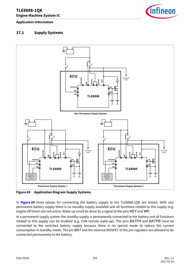
Data Sheet 203 Rev. 1.2 2017-02-10
TLE8888-1QKEngine Machine System IC
Application Information
17.1 Supply Systems
Figure 69 Application Diagram Supply Systems
In Figure 69 three setups for connecting the battery supply to the TLE8888-1QK are shown. With nonpermanent battery supply there is no standby supply available and all functions related to this supply (e.g.engine off timer) are not active. Wake-up could be done by a signal at the pins KEY and WK.In a permanent supply system the standby supply is permanently connected to the battery and all functionsrelated to this supply can be enabled (e.g. CAN remote wake-up). The pins BATPA and BATPB must beconnected to the switched battery supply because there is no special mode to reduce the currentconsumption in standby mode. The pin BAT and the external MOSFET of the pre regulator are allowed to beconnected permanently to the battery.
VG
V6V
BA
TSTB
Y
V5VSTBY
BA
TPA
BATP
B
BAT
WK
KEY
MR
to all other loads
External Wake Up
Circuit
Permanent Supply System 1
ECU
TLE8888
VG
V6V
BA
TSTB
Y
V5VSTBY
BA
TPA
BATP
B
BAT
WK
KEY
MR
to all other loads
External Wake Up
Circuit
Permanent Supply System 2
ECU
TLE8888
VG
V6V
BAT
STB
Y
V5VSTBY
BAT
PA
BAT
PB BAT
WK
KEY
MR
to all other loads
Non Permanent Supply System
ECU
TLE8888

Data Sheet 204 Rev. 1.2 2017-02-10
TLE8888-1QKEngine Machine System IC
Application Information
17.2 VR Sensor InterfaceFor Hall sensor signal detection in Figure 70 and Figure 71 different proposals for the external devices areshown. For the description of the set ups see Chapter 10.
Figure 70 Application Circuit for VR Sensor Interface used for Hall Sensor in Hall Mode Set Up
VROUTVR Sensor Interface
VRIN1
VRIN2
Hall Sensor
Sensor Supply
2-2,5V internaly generated
3 wire Hall Sensor
VR Sensor Interface
VRIN1
VRIN2
Hall Sensor
Sensor Supply
VROUT
2 wire Hall Sensor
2-2,5V internaly generated

Data Sheet 205 Rev. 1.2 2017-02-10
TLE8888-1QKEngine Machine System IC
Application Information
Figure 71 Application Circuit for VR Sensor Interface used for Hall Sensor in Auto, Semi Auto and Manual Detection Mode Set Up
VR Sensor Interface
VRIN1
VRIN2
Hall Sensor
Sensor Supply
2-2,5V
VROUT
2 wire Hall Sensor
VROUTVR Sensor Interface
VRIN1
VRIN2
Hall Sensor
Sensor Supply 3 wire Hall Sensor
2-2,5V
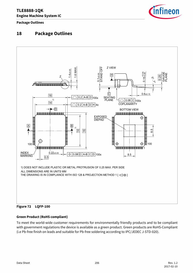
Data Sheet 206 Rev. 1.2 2017-02-10
TLE8888-1QKEngine Machine System IC
Package Outlines
18 Package Outlines
Figure 72 LQFP-100
Green Product (RoHS compliant)To meet the world-wide customer requirements for environmentally friendly products and to be compliantwith government regulations the device is available as a green product. Green products are RoHS-Compliant(i.e Pb-free finish on leads and suitable for Pb-free soldering according to IPC/JEDEC J-STD-020).

Data Sheet 207 Rev. 1.2 2017-02-10
TLE8888-1QKEngine Machine System IC
Revision History
19 Revision History
Revision Date ChangesV1.2 2017-02-10 updated to new layout, package picture (page 5) and package outline picture
(page 206) updated, paragraph below package outline picture removed
V1.1 2014-08-20 on all pages: general name changed to “TLE8888-1QK” and date and revision
V1.1 2014-08-20 page 5 and 6: 2 device types added
V1.1 2014-08-20 page 29: parameter P_5.3.24 min/max changed
V1.1 2014-08-20 page 52: parameter P_7.5.2 and P_7.5.11 max defined
V1.1 2014-08-20 page 57: parameter P_8.8.38, P_8.8.39, P_8.8.40, P_8.8.42, P_8.8.43 and P_8.8.44 definition improved
V1.1 2014-08-20 page 58: parameter P_8.8.45 definition improved
V1.1 2014-08-20 page 62: table 25 corrected
V1.1 2014-08-20 page 100: PGND reference pin changed
V1.1 2014-08-20 page 2, 9, 10, 11, 17, 18, 20, 21, 22, 26, 38, 39, 43, 44, 45, 48, 49, 52, 56, 58, 196: missing variable names added
V1.0 2014-03-13 Data Sheet

Trademarks of Infineon Technologies AGµHVIC™, µIPM™, µPFC™, AU-ConvertIR™, AURIX™, C166™, CanPAK™, CIPOS™, CIPURSE™, CoolDP™, CoolGaN™, COOLiR™, CoolMOS™, CoolSET™, CoolSiC™,DAVE™, DI-POL™, DirectFET™, DrBlade™, EasyPIM™, EconoBRIDGE™, EconoDUAL™, EconoPACK™, EconoPIM™, EiceDRIVER™, eupec™, FCOS™, GaNpowIR™,HEXFET™, HITFET™, HybridPACK™, iMOTION™, IRAM™, ISOFACE™, IsoPACK™, LEDrivIR™, LITIX™, MIPAQ™, ModSTACK™, my-d™, NovalithIC™, OPTIGA™,OptiMOS™, ORIGA™, PowIRaudio™, PowIRStage™, PrimePACK™, PrimeSTACK™, PROFET™, PRO-SIL™, RASIC™, REAL3™, SmartLEWIS™, SOLID FLASH™,SPOC™, StrongIRFET™, SupIRBuck™, TEMPFET™, TRENCHSTOP™, TriCore™, UHVIC™, XHP™, XMC™.
Trademarks updated November 2015
Other TrademarksAll referenced product or service names and trademarks are the property of their respective owners.
Edition 2017-02-10Published by Infineon Technologies AG81726 Munich, Germany
© 2017 Infineon Technologies AG.All Rights Reserved.
Do you have a question about any aspect of this document?Email: [email protected]
IMPORTANT NOTICEThe information given in this document shall in noevent be regarded as a guarantee of conditions orcharacteristics ("Beschaffenheitsgarantie"). With respect to any examples, hints or any typicalvalues stated herein and/or any information regardingthe application of the product, Infineon Technologieshereby disclaims any and all warranties and liabilitiesof any kind, including without limitation warranties ofnon-infringement of intellectual property rights of anythird party. In addition, any information given in this document issubject to customer's compliance with its obligationsstated in this document and any applicable legalrequirements, norms and standards concerningcustomer's products and any use of the product ofInfineon Technologies in customer's applications. The data contained in this document is exclusivelyintended for technically trained staff. It is theresponsibility of customer's technical departments toevaluate the suitability of the product for the intendedapplication and the completeness of the productinformation given in this document with respect tosuch application.
For further information on technology, delivery termsand conditions and prices, please contact the nearestInfineon Technologies Office (www.infineon.com).
WARNINGSDue to technical requirements products may containdangerous substances. For information on the typesin question please contact your nearest InfineonTechnologies office.
Except as otherwise explicitly approved by InfineonTechnologies in a written document signed byauthorized representatives of Infineon Technologies,Infineon Technologies’ products may not be used inany applications where a failure of the product or anyconsequences of the use thereof can reasonably beexpected to result in personal injury.
Please read the Important Notice and Warnings at the end of this document