energy-efficient i/o interface ... - stanford...
TRANSCRIPT

ENERGY-EFFICIENT I/O INTERFACE DESIGN WITH
ADAPTIVE POWER-SUPPLY REGULATION
A DISSERTATION
SUBMITTED TO THE DEPARTMENT OF
ELECTRICAL ENGINEERING
AND THE COMMITTEE ON GRADUATE STUDIES
OF STANFORD UNIVERSITY
IN PARTIAL FULFILLMENT OF THE REQUIREMENTS
FOR THE DEGREE OF
DOCTOR OF PHILOSOPHY
Gu-Yeon Wei
June 2001

ii
© Copyright by Gu-Yeon Wei 2001
All Rights Reserved

v
Abstract
The demand for high-bandwidth and low-power I/O interfaces for intra-chip
communication motivates this work. Aggressive CMOS scaling has enabled higher
performance and integration at the expense of higher power dissipation and design
complexity. This work investigates a technique that adaptively regulates the supply
voltage to minimize power consumption while enabling a simpler I/O design.
Adaptively regulating the supply voltage offers significant energy savings due to
energy’s squared dependence on voltage for digital circuits. In order to find the minimum
voltage required for proper operation at speed, a digital power-supply regulator relies on
an inverter-based model of the worst-case critical path and the model’s ability to track the
delay of the critical path with respect to process and environmental conditions. A purely
digital implementation leads to a robust design that can also benefit from the same power
savings technique as in the load. An experimental prototype demonstrates conversion
efficiencies greater than 90-% across a wide range of regulated voltage levels.
A high-speed parallel I/O interface driven with an adaptively regulated supply can
take advantage of several properties that lead to a simple, low-power solution. In addition
to minimizing power consumption, given the tracking ability of the inverter-based model
of the critical path, the regulated voltage level contains information about process and
operating conditions. This property allows the designer to replace precision analog circuits
with simple digital gates and results in a simpler design. Furthermore, it enables a receiver
design whose bandwidth tracks the bit rate and a transmitter with automatic slew-rate
control. A parallel I/O prototype with adaptive power supply regulation was fabricated in

vi
a 0.35µm CMOS technology. The prototype achieves 0.2-0.8 Gb/s link operation and its
power consumption is a function of the bit rate to a power greater than two.

vii
Acknowledgments
Looking back on the nineties at Stanford, I fondly remember many wonderful
experiences and friendships. Stanford has a dynamic collection of students, teachers, and
staff that encourages one to pursue knowledge in an exciting environment. I will always
cherish my time here.
I am indebted to my adviser, Professor Mark Horowitz, who was kind enough to
support a clueless undergraduate to do research one summer in 1994. Little did he know
that it would last more than six years. I thank Mark for his keen insight, guidance, and
patience throughout the course of my research and thesis. I feel incredibly fortunate to
have had him as my adviser.
I would also like to thank Professor Bruce Wooley for being my associate adviser,
serving on my orals committee, reading this thesis, and continued support throughout the
years in CIS. I am grateful to Professor James Harris and Professor Bob Dutton for also
having served on my orals examination committee. I also extend thanks to Professor Jim
Plummer for being my undergraduate adviser and giving me an opportunity to play in the
clean room for a summer. I am also fortunate to have received technical wisdom and
guidance from Professor Tom Lee.
This research and thesis could not have been possible without the collaboration,
encouragement, and aid of many colleagues. I especially thank Stefanos Sidiropoulos for
his generous help and guidance throughout the design and layout of the test chip and for
reading this thesis. This work also would not have been possible if it were not for the hard
work and dedication of Dean Liu and Jaeha Kim. I am grateful for the discussions and

viii
camaraderie of fellow students, past and present: Dan Weinlader, Birdy Amrutur, Ron Ho,
Ken Mai, Ken Yang, Ricardo Gonzalez, John Maneatis, Arvin Shahani, Derek Shaeffer,
Bennett Wilburn, Patrick Yue, Tom Soh, Adrian Ong, Joe Ingino, and all of the students in
the Wooley, Horowitz and Lee groups.
Outside of school life, I have many people to thank for their continued support and
friendship. Dan Kim, Woo-Young Rhee, Stephen Ryu, Jaeson Kim, Jay Kim, James Yao,
Charles Watson, K.C. Chang and Eugene Jhong have enriched my graduate school years.
Kenny Park, Eddie Ahn, David Kim, Jeehun Hwang, Christian Gehman, Steve Martinez,
Dave Atkins, and countless others have made my undergraduate years memorable. I also
thank Jin Lee for her friendship and support through the last stretch.
Throughout my life, my parents have always supported me with love and prayer. I
dedicate this thesis to them. I am also fortunate to have had three sisters who watched over
their little brother. Lastly, I am grateful for my nieces and nephew, who were always so
loving and cheerful.

ix
Table of Contents
Abstract..........................................................................................................v
Acknowledgments .......................................................................................vii
List of Figures...............................................................................................xi
List of Tables ...............................................................................................xv
Chapter 1 Introduction.................................................................................11.1 Low-Power Techniques.....................................................................................11.2 CMOS Parallel Links ........................................................................................31.3 Organization ......................................................................................................4
Chapter 2 Background .................................................................................72.1 Power and Delay in Digital CMOS Circuits .....................................................82.2 Delay Tracking ................................................................................................14
2.2.1 Inverter-based tracking......................................................................142.2.2 Other non-ideal effects ......................................................................182.2.3 Delay Tracking Summary .................................................................21
2.3 Adaptive power supply regulation ..................................................................222.3.1 Buck Converter .................................................................................222.3.2 PID Control Loop..............................................................................26
2.4 Summary .........................................................................................................29
Chapter 3 Digital Power-Supply Controller.............................................313.1 A/D Conversion...............................................................................................323.2 Digital PID Control .........................................................................................363.3 Variable-Frequency Control............................................................................393.4 Low-Power Control .........................................................................................473.5 Non-Linear Power Reduction Techniques ......................................................513.6 Summary .........................................................................................................54

x
Chapter 4 I/O Interface Design..................................................................574.1 Overview of parallel links ...............................................................................58
4.1.1 Critical-path delay.............................................................................604.1.2 Signal Integrity..................................................................................62
4.2 Finding the “right” voltage..............................................................................634.2.1 Summary ...........................................................................................76
4.3 Transmitter Design ..........................................................................................774.3.1 High-Impedance Drivers ...................................................................784.3.2 Impedance, Current and Slew-Rate Control .....................................814.3.3 Transmitter Summary........................................................................84
4.4 Receiver Design ..............................................................................................844.4.1 Bandwidth-Tracking Preamplifier ....................................................864.4.2 Regenerative Latch and Timing ........................................................894.4.3 Receiver Summary ............................................................................90
4.5 Timing Recovery.............................................................................................914.5.1 Dual-loop architecture.......................................................................924.5.2 Digital interpolation ..........................................................................944.5.3 Duty-cycle adjuster ...........................................................................974.5.4 Clock Distribution and Relative Timing ...........................................984.5.5 Timing Recovery Summary ..............................................................99
4.6 Experimental Results.....................................................................................1004.6.1 Test-chip Components and Testing Circuitry .................................1014.6.2 Dual-Loop DLL ..............................................................................1024.6.3 I/O Transceiver................................................................................1054.6.4 Power Breakdown Analysis ............................................................108
4.7 Summary .......................................................................................................110
Chapter 5 Conclusions ..............................................................................111
References ..................................................................................................115

xi
List of Figures
Figure 1.1. Link components..........................................................................................4Figure 2.2. Normalized delay and frequency vs. supply voltage ...................................9Figure 2.3. Normalized power vs. normalized frequency ..............................................9Figure 2.4. Normalized energy vs. normalized frequency ...........................................10Figure 2.5. Normalized frequency vs. supply voltage vs. corners ...............................11Figure 2.6. Normalized energy vs. normalized frequency vs. corners .........................12Figure 2.7. Normalized frequency vs. supply voltage vs. temperature ........................13Figure 2.8. Normalized delay tracking of various complex static and dynamic gate vs.
process corner ............................................................................................15Figure 2.9. Normalized delay tracking of various complex static and dynamic gates
vs. temperature...........................................................................................16Figure 2.10. Delay tracking of various static and complex gates normalized to Lmin
FO4 inverter vs. supply voltage.................................................................16Figure 2.11. Delay tracking of various static and complex gates normalized to 1.5*Lmin
FO4 inverter vs. supply voltage.................................................................17Figure 2.12. Wire delay test bench and RC model.........................................................19Figure 2.13. Wire delay tracking vs. supply voltage......................................................19Figure 2.14. Normalized effective inverter gate capacitance vs. supply voltage ...........20Figure 2.15. Buck converter ...........................................................................................23Figure 2.16. Buck converter switching transistor power loss vs. width.........................25Figure 2.17. Control-loop block diagram.......................................................................26Figure 2.18. PID control-loop frequency-domain model ...............................................27Figure 2.19. PID control open-loop frequency response ...............................................28Figure 2.20. PWM rectangular wave generation............................................................29Figure 3.1. Digital controller block diagram................................................................31Figure 3.2. Ring oscillator and counter based A/D converter ......................................32Figure 3.3. A/D converter detailed schematic..............................................................33Figure 3.4. Low-power A/D converter.........................................................................35Figure 3.5. Circuit implementation of PID control blocks...........................................37

xii
Figure 3.6. Digital PID control loop ............................................................................39Figure 3.7. Normalized power breakdown...................................................................41Figure 3.8. Normalized frequency shifting ..................................................................42Figure 3.9. Simulated open-loop response at high and low loop-frequency limits......43Figure 3.10. Simulated voltage-transient response ........................................................43Figure 3.11. Test-chip micrograph .................................................................................44Figure 3.12. Overhead power vs. regulated voltage.......................................................44Figure 3.13. Conversion efficiency vs. regulated voltage..............................................45Figure 3.14. Measured load transient response ..............................................................46Figure 3.15. Measured voltage transient response .........................................................46Figure 3.16. Low-power D/A block diagram.................................................................48Figure 3.17. Low-power controller block diagram ........................................................49Figure 3.18. Low-to-high voltage converter ..................................................................50Figure 3.19. Power-supply controller block photo micrograph (zoom).........................51Figure 3.20. Segmented buck converter switching transistors.......................................52Figure 3.21. Recirculating current detector....................................................................54Figure 4.1. Link components........................................................................................58Figure 4.2. Source synchronous parallel interface .......................................................59Figure 4.3. Clock swing magnitude vs. clock period ...................................................61Figure 4.4. Delay-locked loop block diagram..............................................................64Figure 4.5. Regulating amplifier loaded with delay-line .............................................65Figure 4.6. Open-loop frequency response (VCTRL = 2.6-V) ......................................66Figure 4.7. Simulated amplifier power vs. Vctrl..........................................................67Figure 4.8. Power supply rejection transient response.................................................68Figure 4.9. Normalized delay-line delay vs. supply voltage ........................................70Figure 4.10. Normalized KDL vs. frequency..................................................................71Figure 4.11. Differential charge pump ...........................................................................72Figure 4.12. Phase-only detector....................................................................................74Figure 4.13. Phase detector transient waveforms...........................................................75Figure 4.14. Low-to-high swing converter.....................................................................76Figure 4.15. Ideal high-impedance driver ......................................................................78Figure 4.16. Single-ended transmitter ............................................................................79Figure 4.17. Differential signaling .................................................................................81Figure 4.18. transmitter output swing control ................................................................82Figure 4.19. Transmitter predriver .................................................................................84Figure 4.20. Receiver block diagram .............................................................................85Figure 4.21. Preamplifier schematic ..............................................................................86Figure 4.22. Preamplifier differential output versus process corner ..............................87Figure 4.23. Preamplifier differential output versus bit rate ..........................................88Figure 4.24. Regenerative latch and SRFF ....................................................................89

xiii
Figure 4.25. Receiver timing..........................................................................................90Figure 4.26. Digital peripheral loop ...............................................................................93Figure 4.27. Phase interpolation.....................................................................................95Figure 4.28. Digital interpolator.....................................................................................95Figure 4.29. Measured interpolation histogram .............................................................96Figure 4.30. Duty-cycle adjuster schematic ...................................................................97Figure 4.31. Duty-cycle adjustment ...............................................................................98Figure 4.32. Test-chip micrograph ...............................................................................101Figure 4.33. Regulated voltage vs. frequency..............................................................102Figure 4.34. DLL jitter histogram -- (a) core, (b) dual.................................................103Figure 4.35. Dual-loop DLL power consumption vs. frequency .................................104Figure 4.36. Single-ended and differential link power vs. bit rate ...............................106Figure 4.37. Minimum transmission swing vs. bit rate ................................................107Figure 4.38. Transmitted eye at 0.8-Gb/s .....................................................................108Figure 4.39. Power breakdown at 800Mb/s .................................................................109

xiv

xv
List of Tables
Table 4.1. Dual-loop DLL performance summary................................................... 104
Table 4.2. Transmitter output slew-rate vs. bit rate.................................................. 108
Table 5.1 I/O test chip performance summary ........................................................ 113

xvi

1
Chapter 1
Introduction
Aggressive CMOS technology scaling has enabled explosive growth in the integrated
circuits (IC) industry with cheaper and higher performance chips. However, these
advancements have led to some chips being limited by the chip-to-chip data
communication bandwidth. This limitation has motivated research in the area of
high-speed links that interconnect chips [21],[37],[47],[52] and has enabled a significant
increase in achievable communication bandwidths. Enabling higher I/O speed and more
I/O channels further improves bandwidth, but these approaches also increase power
consumption that eats into the overall power budget of the chip. In addition, complexity
and area become major design constraints when trying to integrate hundreds of links on a
single chip. Therefore, there is a need for building high performance I/O interfaces with
low power consumption and low design complexity. This thesis explores using a
technique that dynamically scales the supply voltage, called adaptive power supply
regulation, to achieve these goals. Controlling the on-chip supply voltage so that the delay
of an inverter is a fixed fraction of a bit time allows one to replace precision analog
circuits with digital CMOS gates and reduce overall power consumption at the same time.
1.1 Low-Power Techniques
Performance of digital systems has been increasing exponentially, driven by higher
clock frequencies and higher chip complexity. Unfortunately, power in digital systems has
also increased as a result and has become a primary concern. Modern high-performance
microprocessors can consume more than 100 W [17],[21] and require special cooling and
power supply systems. The recent proliferation of portable devices also emphasizes the

2 Chapter 1. Introduction
need for lowering power dissipation, requiring chips with lower energy consumption to
extend battery life.
Power in synchronous CMOS digital systems is dominated by their dynamic power
dissipation, which is governed by the following equation:
Pdynamic = α Csw VDD Vswing fclk, (1-1)
where α is the switching activity, Csw is the total switched capacitance, VDD is the supply
voltage, Vswing is the internal swing magnitude of signals (usually equals Vdd for most
CMOS gates), and fclk is the frequency of operation. And since power is the rate of change
of energy,
E = α Csw VDD Vswing. (1-2)
Technology scaling enables lower power and energy since when a chip transitions to a
new scaled technology, both capacitance and voltage decrease for this chip. Scaling
technology also means that the gates get faster, so it is possible to run this scaled chip at
higher frequencies, while still dissipating less power than before.
Aside from technology scaling, reducing just the supply voltage for a given
technology enables significant reduction in power and energy; both are proportional to the
supply voltage squared. However, voltage reduction comes at the expense of slower gate
speeds. So, there is a trade-off between performance and energy consumption.
Recognizing this relationship between supply voltage and circuit performance,
dynamically adjusting the supply voltage to the minimum needed to operate at a given
frequency enables one to reduce the energy consumption down the minimum required.
This technique is referred to as adaptive power supply regulation, and requires a
mechanism that tracks the worst case delay path through the digital circuitry with respect
to process, temperature and voltage in order to determine the minimum supply voltage
required for proper operation.
There have been several examples of this power saving technique applied to general
purpose microprocessors [4],[29],[38],[46] and digital signal processing (DSP) chips

Chapter 1. Introduction 3
[5],[15],[35] for mobile and other applications where minimizing energy consumption is a
priority. These systems commonly rely on the bursty nature of their operation to
dynamically adjust the speed and supply voltage in order to minimize the energy
consumed for the required computational tasks at hand. Furthermore, these systems
employ both hardware and software based schemes to monitor the computational needs of
the system.
Adaptive power supply regulation can be used for more than optimizing energy
consumption based on the varying computational needs of a digital chip in time. It can
also be used for varying computational needs of different parts within a chip. An extreme
example of this would be to partition large, somewhat autonomous blocks within a digital
chip and operate them at their own optimum frequency and voltage. However, the
overhead associated with communication between the potentially asynchronous blocks
and to efficiently provide separate voltages to each of them is a formidable challenge. A
subset of this example would be to identify a block within a digital chip that consumes a
significant component of the overall power and could operate at a lower supply voltage. In
other words, a block whose critical delay paths are much shorter than the rest of the digital
chip such that, as a separate entity, it could operate at a much lower voltage for the same
clock rate. We will see throughout this thesis that a high-speed parallel interface for
high-bandwidth communication between chips meets these criterion and its function is
briefly introduced next.
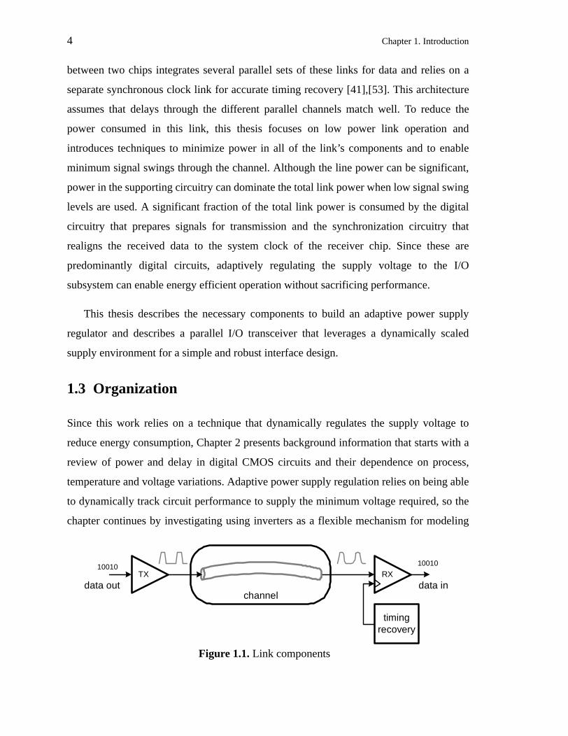
1.2 CMOS Parallel Links
High-speed links can provide high communication bandwidth between chips and consist
of four main components as shown in Figure 1.1. A transmitter converts digital binary
data into electrical signals that travel through the channel. This channel is normally
modeled as a transmission line and can consist of traces on a printed circuit board (PCB),
coaxial cables, shielded or un-shielded twisted pair wires, traces within chip packages, and
the connectors that join these various parts together. A receiver then converts the incoming
signal back to digital data and requires a timing recovery block to compensate for delay
through the channel. A common architecture to enable high bandwidth communication
4 Chapter 1. Introduction
between two chips integrates several parallel sets of these links for data and relies on a
separate synchronous clock link for accurate timing recovery [41],[53]. This architecture
assumes that delays through the different parallel channels match well. To reduce the
power consumed in this link, this thesis focuses on low power link operation and
introduces techniques to minimize power in all of the link’s components and to enable
minimum signal swings through the channel. Although the line power can be significant,
power in the supporting circuitry can dominate the total link power when low signal swing
levels are used. A significant fraction of the total link power is consumed by the digital
circuitry that prepares signals for transmission and the synchronization circuitry that
realigns the received data to the system clock of the receiver chip. Since these are
predominantly digital circuits, adaptively regulating the supply voltage to the I/O
subsystem can enable energy efficient operation without sacrificing performance.
This thesis describes the necessary components to build an adaptive power supply
regulator and describes a parallel I/O transceiver that leverages a dynamically scaled
supply environment for a simple and robust interface design.
1.3 Organization
Since this work relies on a technique that dynamically regulates the supply voltage to
reduce energy consumption, Chapter 2 presents background information that starts with a
review of power and delay in digital CMOS circuits and their dependence on process,
temperature and voltage variations. Adaptive power supply regulation relies on being able
to dynamically track circuit performance to supply the minimum voltage required, so the
chapter continues by investigating using inverters as a flexible mechanism for modeling
TX RXdata in
timingrecovery
channel
10010
data out
10010
Figure 1.1. Link components

Chapter 1. Introduction 5
critical path delay. It then reviews the components necessary to build an adaptive power
supply regulator by looking at the characteristics of a buck converter that creates a lower
regulated voltage, and the resulting feedback control loop architecture. For effective
application to digital systems, Chapter 3 describes a digital implementation of an
inherently analog power supply control loop.
Chapter 4 describes how applying this power saving technique to an I/O subsystem
leads to a simple and low-power design. A core DLL, which is a necessary component for
timing recovery in the interface, also serves the dual role of determining the “right”
voltage of operation with respect to frequency by tracking the worst case delay path in the
I/O subsystem. The chapter then describes issues associated with building transceiver
circuit components that can function in a variable voltage environment, and presents the
resulting transmitter and receiver designs. Another key component of the link is the timing
recovery block, which can also leverage the adaptively regulated voltage environment to
yield a simpler, mostly digital implementation. The circuit implementations of the
building blocks are described and experimentally measured results from a fabricated
test-chip prototype present the power savings offered by adaptively regulating the supply
voltage that drives the I/O subsystem.

6 Chapter 1. Introduction
7
Chapter 2
Background
This work focuses on a power-saving technique for digital CMOS circuits that
dynamically lowers the supply voltage down to the minimum required for proper
operation. By tracking the variable process and environmental effects on circuits, the
supply voltage can be regulated to operate circuits at their most energy efficient point
without special circuit techniques or logic families, and can be applied to standard static
CMOS logic gates. The ability to determine the minimum voltage required for operation
requires two components: (i) a mechanism to track circuit performance (or delay) with
respect to process, temperature and voltage, and (ii) an efficient power supply regulator to
power the digital CMOS circuits. These two issues are the main topics for this chapter.
While simply adjusting the supply voltage to preset levels relative to discrete clock
frequencies, set by system performance requirements, enables power reduction, we must
also consider the inefficiencies due to overhead voltage margins that are normally
imposed on digital circuits. Therefore, before looking at delay tracking mechanisms,
Section 2.1 first looks at how process and operating parameters affect circuit performance
and power dissipation in digital circuits. Although circuit delay is roughly inversely
proportional to supply voltage, process variations and environmental conditions affect
device parameters to cause delay and performance variations. By using a unit inverter as
being representative of general digital CMOS circuits, we can investigate the energy
savings offered with an adaptive power supply regulation scheme that is aware of local
process and operating conditions. The assumption that inverters can be used to model the
performance of general circuits requires the delay of complex gates track the delay of an
inverter across a variety of parameters that affect performance. Section 2.2 investigates the

8 Chapter 2. Background
delay tracking ability of inverters with respect to process, temperature, and voltage
variations, and identifies some caveats of simply using inverters as a delay tracking
mechanism. An efficient switching power supply regulator design that can enable this
power savings is the subject of the rest of this chapter.
2.1 Power and Delay in Digital CMOS Circuits
The delay of digital CMOS circuits depends on three main parameters: (i) process, (ii)
temperature, and (iii) supply voltage. Variability in manufacturing results in chips that
exhibit a range of performance due to variations in device thresholds, oxide thicknesses,
doping profiles, etc. Operating conditions also affect performance. Temperature affects the
mobility of holes and electrons, and also the transistor’s threshold voltage. Lastly, circuit
delay strongly depends on supply voltage. The delay of a static CMOS gate can be
approximated by the following equation:
(2-1)
where Cload is the load it drives, Vswing is the swing magnitude of the output (which is Vdd
for static CMOS gates), Vdd is the supply voltage, and β(Vdd-VTH)α models the device
current [39]. For low fields, α is around 2, but for modern devices α is as low as 1.25 [20].
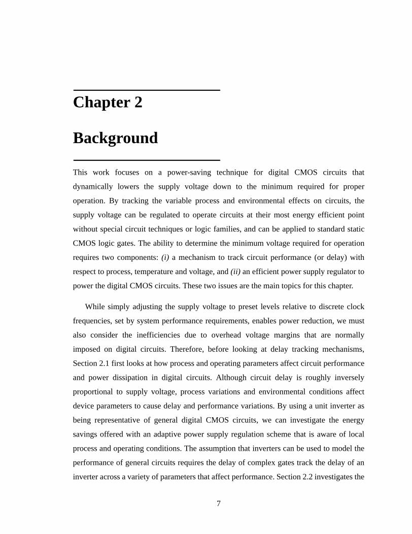
Delay variation of a typical fanout-of-4 (FO4) inverter1 versus supply voltage in an
HP0.35µm CMOS process is shown in Figure 2.2 and matches extremely well with the
above delay equation for α=1.4. Assuming that the critical path delay of a digital system is
a function of some number of inverter delays2, the normalized frequency of operation
versus supply voltage can be found by inverting and normalizing the inverter’s delay and
is also presented in Figure 2.2. The frequency of operation achievable by a chip is roughly
1 A fanout-of-4 inverter is an inverter that driver another inverter with four times its own input capacitance.2 Section 2.2 shows that a string of inverters can be used to model the critical path delay of digital circuits,
consisting of a variety of complex gates, and it tracks well over a wide range of process corners andtemperatures. Although the delay of complex gates do not track as well over a wide range of voltage,Section 4.1.1 shows that a string of inverters is a good model for the I/O subsystem’s critical path.
delay
CloadVswing
β Vdd VTHÐ( )α----------------------------------------∝
Chapter 2. Background 9
linear with supply voltage. This way of visualizing relative circuit performance versus
supply voltage is used extensively throughout this section to analyze the effects of
different parameters on performance and power.
To understand what this relationship means for power, the delay data is applied to the
dynamic power equation (Equation 2-1) and the resulting normalized power is plotted
relative to normalized frequency for two supply voltage configurations in Figure 2.3.
Figure 2.2. Normalized delay and frequency vs. supply voltage
0
0.5
1
1.5
2
2.5
3
3.5
4
4.5
1 1.5 2 2.5 3 3.5
0.2
0.4
0.6
0.8
1
Inve
rter
Del
ay(n
s)
No
rmal
ized
Fre
qu
ency
Supply Voltage
0
0.5
1
1.5
2
2.5
3
3.5
4
4.5
1 1.5 2 2.5 3 3.5
0.2
0.4
0.6
0.8
1
Inve
rter
Del
ay(n
s)
No
rmal
ized
Fre
qu
ency
Supply Voltage
Figure 2.3. Normalized power vs. normalized frequency
0.0 0.2 0.4 0.6 0.8 1.0
Normalized Frequency
0.0
0.2
0.4
0.6
0.8
1.0
No
rmal
ized
Dyn
amic
Po
wer
Fixed VddVariable Vdd
PowerSavings

10 Chapter 2. Background
Given a fixed supply voltage, power consumption is proportional to frequency, resulting
in a straight line in this figure. Since gate delay can increase if the required operating
frequency is reduced, the circuit can operate at lower supply voltages. Therefore, further
power savings are possible by reducing the supply voltage to the value indicated by Figure
2.2, for each lower operating frequency. Now, power consumption reduces dramatically
for lower frequencies and is proportional to frequency cubed. Another way to analyze this
savings is to look at the energy consumed per operation, where an operation is assumed to
complete within some fixed number of clock cycles [3]. Figure 2.4 plots the normalized
energy consumption per operation versus normalized frequency, again for two voltage
conditions. Since the energy consumed is independent of frequency, it is constant
regardless of frequency for a fixed supply voltage. However, by appropriately adjusting
the supply voltage, there is a quadratic relationship between energy and frequency.
Therefore, significant energy savings is possible by operating the chip at lower than peak
frequencies.
In addition to the energy savings possible by adaptively regulating the power supply
down to lower levels for lower frequencies, there is a potential for saving energy due to
inefficiencies found in conventional digital designs that operate off a fixed supply voltage.
Variability in circuit performance due to process and temperature variations require
Figure 2.4. Normalized energy vs. normalized frequency
0
0.2
0.4
0.6
0.8
1
0 0.2 0.4 0.6 0.8 1
No
rmal
ized
En
erg
y/O
per
atio
n
Workoad (Normalized Frequency)
Fixed Vdd = 3.3V
Dynamically scaled Vdd
Energy Savings2VCE ⋅∝
0
0.2
0.4
0.6
0.8
1
0 0.2 0.4 0.6 0.8 1
No
rmal
ized
En
erg
y/O
per
atio
n
Workoad (Normalized Frequency)
Fixed Vdd = 3.3V
Dynamically scaled Vdd
Energy Savings2VCE ⋅∝

Chapter 2. Background 11
conventional designs incorporate overhead voltage margins to guarantee proper operation
under worst-case conditions. This is due to the circuit delay’s strong dependence on
process parameters and temperature as shown by the equations for device
transconductance, β, and threshold voltage, VTH, below. [33]
(2-2)
(2-3)
Device transconductance strongly depends on oxide thickness, Cox, which can vary by
12-% between process runs1. Mobility and threshold voltage both have strong dependence
on temperature which can significantly degrade circuit speed. Performance dependence on
process and temperature can be exemplified by plotting the normalized frequency vs.
supply voltage under typical (typical nMOS, typical pMOS, 25-C), fast (fast nMOS, fast
pMOS, 0-C), and slow (slow nMOS, slow pMOS, 100-C) corners, shown in Figure 2.5.
1 Oxide thickness variation based on COX parameters for corner case BSIM models for HP0.35µm process.
β µn p, CoxWL-----=
TH VT0 γ 2φFÐ VSBÐ 2φFÐ( )+=
0.5 1 1.5 2 2.5 3 3.50
0.2
0.4
0.6
0.8
1
1.2
1.4
No
rmal
ized
Fre
qu
ency
Supply Voltage (V)
FAST
TYP
SLOW
74%
Figure 2.5. Normalized frequency vs. supply voltage vs. corners

12 Chapter 2. Background
Although a chip may be able to operate at a peak normalized frequency of 1, under typical
conditions and 3.3-V, slow device corners and high temperature degrade circuit
performance so that it is unable to function properly at the high target speed. To
accommodate this performance variation, chips are normally run at frequencies lower than
the normalized peak, identified in the figure at 74-% as an example. Although a slow
corner chip can now properly function at this lower frequency, typical and fast corner
chips incur large voltage overheads, with a supply fixed at 3.3-V, of 1-V and 1.4-V
respectively. This overhead translates into excess power dissipated to allow margins for
worst case corners. By taking a look at the energy consumed per operation versus
frequency again, as shown in Figure 2.6, since chips under typical and process and
temperature conditions can operate at higher speeds with a lower supply voltage and due
to energy’s quadratic dependence on voltage, not only is energy conserved compared to
the fixed supply case, but significant savings is possible at typ and fast corners compared
to the slow corner.
A common technique employed by the IC industry to deal with process variability is
called speed binning and is common practice for commodity parts such as semiconductor
memories and microprocessors. Fabricated chips are categorized into different groups
0 0.2 0.4 0.6 0.8 1 1.20
0.2
0.4
0.6
0.8
1
1.2
No
rmal
ized
En
erg
y
Workload (Normalized Frequency)
SLOW
TYP
FAST
Figure 2.6. Normalized energy vs. normalized frequency vs. corners

Chapter 2. Background 13
based on the maximum speeds that can be achieved. Although binning allows
manufacturers to deal with process variability, operating temperature generally cannot be
known a priori and therefore chips still need margins to be meet specifications over a wide
range of temperatures. Figure 2.7 reveals that chip performance strongly depends on
temperature and in order to guarantee operation at the worst case temperature, presented
as 130-C, specification at lower speed is inevitable and a potentially large voltage
overhead again results for a fixed supply voltage. By actively tracking on-die
environmental conditions, namely temperature, dynamic supply voltage regulation
accommodates the differences imposed by temperature variations to minimize energy
consumption. Furthermore, since temperatures can vary over time, active compensation is
necessary to eliminate this time-varying effect on performance, and is not possible with
one-time binning after fabrication.
This analysis of how an inverter’s speed and power consumption changes relative to
process and operating conditions shows there is a potential for considerable power savings
due to a large voltage overhead incurred with a fixed supply voltage. While much of the
overhead may be reduced, the actual savings that can be achieved depends on how well
Figure 2.7. Normalized frequency vs. supply voltage vs. temperature
0
0.2
0.4
0.6
0.8
1
1.2
1 1.5 2 2.5 3 3.5
No
rmal
ized
Fre
qu
ency
Supply Voltage (V)
0 50 130
0.8 V
0.88
0
0.2
0.4
0.6
0.8
1
1.2
1 1.5 2 2.5 3 3.5
No
rmal
ized
Fre
qu
ency
Supply Voltage (V)
0 50 130
0.8 V
0.88

14 Chapter 2. Background
the critical path’s delay tracks relative to an inverter’s delay (or the delay of circuit that
models the critical path) versus process, voltage, and temperature (PVT). Mismatches
between the two lead to margins required to guarantee proper circuit operation. Therefore,
the next section investigates how well the delay of several complex gates track the delay
of an inverter across PVT.
2.2 Delay Tracking
The ability to actively track the performance of digital circuits with respect to local
process and temperature variations enables the circuits to operate at a more energy
efficient point. Since the performance of a digital system is limited by its worst case
critical path delay, an exact replica of this delay path is one of the most accurate ways to
measure delay variation with respect to different process corners and variations in
operating conditions within a single chip. However, in real designs, designers normally
balance delay paths within digital blocks as much as possible. Therefore, identifying a
single path to replicate may be difficult. Furthermore, critical paths may differ depending
on process corner and operating environment. Instead, we will consider using a series
chain of inverters to model the critical path delay. This approach relies on a basic
assumption that the delay of complex gates that make-up the critical path track the delay
of an inverter. Section 2.2.1 investigates how well the delay of several static and dynamic
gates track an inverter’s delay. Mismatches measured across voltage variations set the
margins necessary for an adaptively supply regulation scheme that use inverters to model
the critical path. In addition to matching pure gate delays, the ability to track the delay of
wires is also important in modern VLSI systems. Section 2.2.2 this and other non-ideal
effects on inverter delay tracking.
2.2.1 Inverter-based tracking
A static CMOS inverter is the simplest unit logic gate and can account for a significant
portion of the total gate count in digital IC’s. It is the primary gate used for clock
distribution and the most efficient mechanism for ramping up drive strength to drive large
capacitive loads. Chapter 1 mentioned that an inverter’s delay variation versus process,

Chapter 2. Background 15
temperature and voltage can be used to predict general circuit performance trends. In this
subsection, we look at how valid that assumption is by measuring the delay of various
static and dynamic complex gates (nand2, nand3, nor2, nor3, transmission gate,
dynamic-nand2, -nand3, -nor2, and -nor3) relative to an inverter delay, across a wide
range of process corners, temperatures and voltages. Results are presented in terms of its
tracking variation with respect to the variable on the x-axis, by taking the normalized
delay of the gates with respect to a FO4 inverter and then calculating how much it varies
relative to a fixed point on the x-axis value. Delay tracking variations versus process
corner are presented first, in Figure 2.8, where FS denotes the fast nMOS, slow pMOS
process corner. The lines are all relatively flat which is an indication that delay of these
gates track well with the delay of an inverter across different process corners. The same
holds true for tracking with respect to temperature as shown in Figure 2.9, where
temperature ranges from 0-C to 130-C. Unfortunately, tracking is not as good across a
wide range of supply voltages, presented in Figure 2.10. Variations in normalized delay
can be attributed to velocity saturation which affects short-channel devices more than
longer-channel devices. If we take a NAND3 for example, there is a series stack of three
nMOS devices which must all be conducting to pull the output low. This stack of three
Figure 2.8. Normalized delay tracking of various complexstatic and dynamic gate vs. process corner
0.94
0.96
0.98
1
1.02
1.04
1.06
SF ST TF SS TT FF TS FT FS
Nor
mal
ized
FO
4D
elay
Var
iatio
n
Process Corner (nMOS, pMOS)
4.7%

16 Chapter 2. Background
minimum channel length devices can be modeled as a single device with an effective
channel length that is three times longer. An inverter, on the other hand, consists of a
single minimum channel length nMOS device. Higher lateral electrical fields saturate the
velocity of carriers in shorter channels lengths more than in longer channels. This
Figure 2.9. Normalized delay tracking of various complexstatic and dynamic gates vs. temperature
0.94
0.96
0.98
1
1.02
1.04
1.06
0 20 40 60 80 100 120 140
Nor
mal
ized
FO
4D
elay
Var
iatio
n
Temperature (C)
5.3%
Figure 2.10. Delay tracking of various static and complex gatesnormalized to Lmin FO4 inverter vs. supply voltage
0.9
0.95
1
1.05
1.1
1.15
1.2
1 1.5 2 2.5 3 3.5
Nor
mal
ized
FO
4D
elay
Var
iatio
n
Supply Voltage (V)
nand3 (14%)
dynamic-and3 (28%)
Chapter 2. Background 17
saturation makes the current in an inverter less sensitive to Vdd, and thus the delay of a
NAND3 increases faster than an inverter as the supply voltage decreases. As a result, the
lines slope downward as supply voltage increases to varying degrees depending on the
gate. The worst case critical path delay occurs at the lowest supply voltage. This
unfortunately means that the extra voltage margins required for lower voltages leads to
excess power consumption at higher speeds and voltages when the chip consumes more
power.
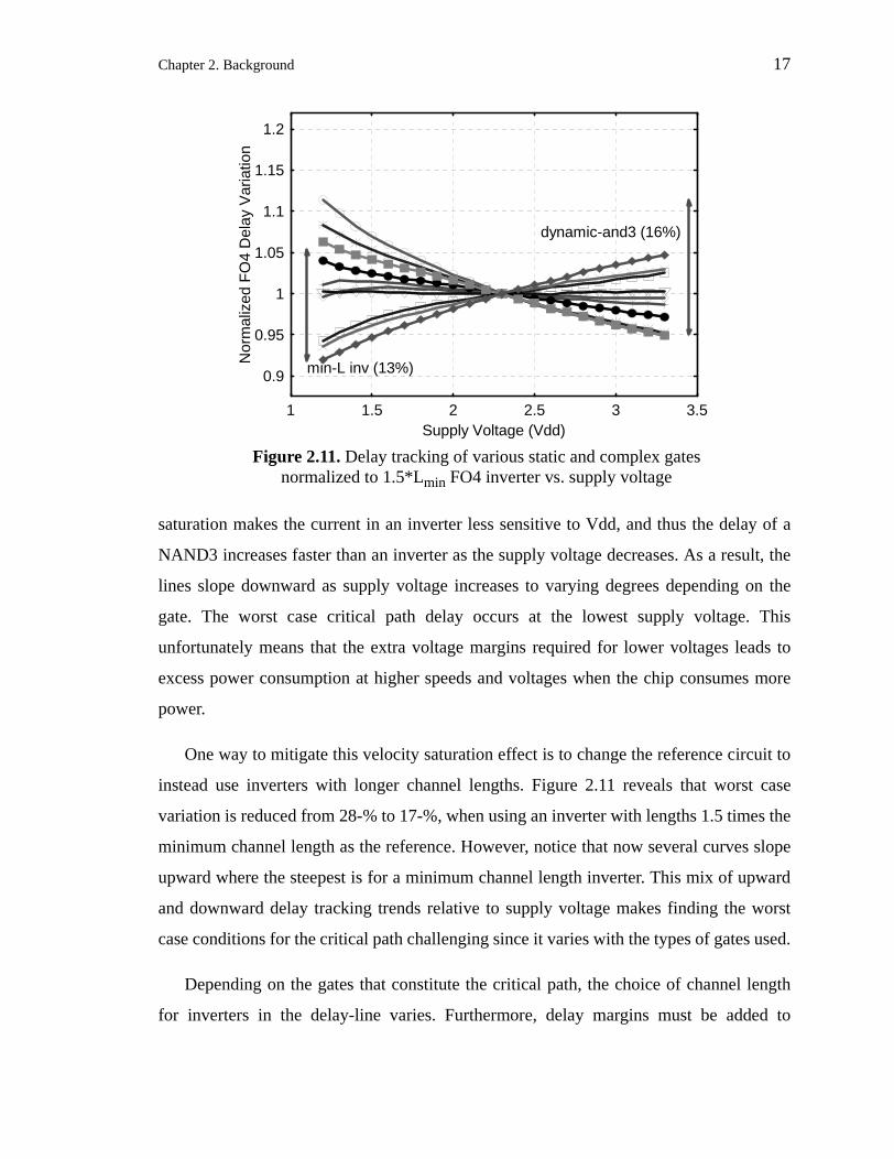
One way to mitigate this velocity saturation effect is to change the reference circuit to
instead use inverters with longer channel lengths. Figure 2.11 reveals that worst case
variation is reduced from 28-% to 17-%, when using an inverter with lengths 1.5 times the
minimum channel length as the reference. However, notice that now several curves slope
upward where the steepest is for a minimum channel length inverter. This mix of upward
and downward delay tracking trends relative to supply voltage makes finding the worst
case conditions for the critical path challenging since it varies with the types of gates used.
Depending on the gates that constitute the critical path, the choice of channel length
for inverters in the delay-line varies. Furthermore, delay margins must be added to
Figure 2.11. Delay tracking of various static and complex gatesnormalized to 1.5*Lmin FO4 inverter vs. supply voltage
0.9
0.95
1
1.05
1.1
1.15
1.2
1 1.5 2 2.5 3 3.5
Nor
mal
ized
FO
4D
elay
Var
iatio
n
Supply Voltage (Vdd)
min-L inv (13%)
dynamic-and3 (16%)

18 Chapter 2. Background
guarantee operation across all voltage conditions. As an example, let us choose 2.3-V to
be the nominal voltage condition for design and we have a choice between two channel
lengths: Lmin and 1.5*Lmin. If the critical path consists mostly of dynamic-and3 gates,
extra delay margin is necessary to guarantee proper operation under low frequency and
low supply conditions. But utilizing longer channel length inverters to model its delay
reduces the margin from 18-% to 12-%. On the other hand, if the critical path consists
mostly of minimum channel length inverters, using 1.5*Lmin inverters to model its
critical path requires an additional 5-% delay margin to guarantee operation under high
speed and voltage conditions. Instead, using minimum channel length inverters in the
delay line would be best. In fact, matching the delay-line elements with the gates that
dominate the critical path would yield the best matching. Chapter 4 shows that an inverter
chain is a good match for an I/O subsystem because the worst case delay path is in the
clock distribution network which predominantly consists of inverters.
2.2.2 Other non-ideal effects
In addition to gate delays, critical paths consist of wires that interconnect different
gates and functional blocks together. The delay through these wires are not governed by
the same physical principles as in MOS gates. Therefore, it is important to consider how
tracking varies when appreciable wire loading is present. In large digital systems, the
delay associated with driving long busses across a chip can be large and often require
repeater buffers to cut down the quadratic dependence on length to a linear one [1],[16].
This analysis utilizes a simple test-bench circuit consisting of inverters interconnected
with a distributed π-model for a wire of variable lengths, as shown in Figure 2.12.
Relatively large device sizes and wire lengths are used in order for wire resistance to be
non-negligible. By modeling the inverter with an output resistance (Rgate), this test bench
reduces to a simple RC model for delay given by the following equation:
. (2-4)
The simulated delays of an inverter with wires (of different lengths ranging from 500-µm
to 3000-µm and 1-µm wide) normalized to an inverter delay without wires, but with the
Tdelay Rgate Cgate Cwire+( )⋅ Rwire Cgate
Cwire
2--------------+
⋅+=

Chapter 2. Background 19
same effective fanout at 3.3-V, versus supply voltage are presented in Figure 2.13. Wire
lengths and effective fanouts with the wire loading are labeled on the graph. Across this
wide range of lengths, delay tracking varies less than 12-% across a wide supply voltage
range. As supply voltage decreases, inverter drive strength reduces and Rgate increases. As
Cwire/2 Cwire/2
Rwire
16µm/8µm16µm/8µm
A B
Rgate
RgateCwire/2 Cwire/2 Cgate
Rwire
Figure 2.12. Wire delay test bench and RC model
Figure 2.13. Wire delay tracking vs. supply voltage
0.95
1
1.05
1.1
1.15
0.5 1 1.5 2 2.5 3 3.5
Nor
mal
ized
Del
ayT
rack
ing
Supply Voltage (Vdd)
500u (3.2)
1000u (5.4)
1500u (7.6)
2000u (9.8)
3000u (14)
wire-L (FO)

20 Chapter 2. Background
a result, one would expect the contribution of wire delay to become less significant and
result in an upward slope in the delay vs. voltage plot. However, the opposite is observed
for wire lengths less than 2000-µm. This can be attributed to a reduction in the effective
gate capacitance on inverters as supply voltage decreases, as shown in Figure 2.14. Once
the load is almost entirely dominated by the wire, the expected upward trend is observed,
which is for wire lengths greater than 2000-µm in this example. In the case of long wires
that use repeaters to linearize delay with respect to distance (versus a quadratic
relationship for non-repeated wires), since optimal fanout is on the order of 4, additional
delay margins of up to 8-% will be necessary to meet the worst-case delay conditions
occurring at low supply voltages.
Apart from variations due to velocity saturation effects and wires, the inverter model
of the critical path must also consider other non-ideal effects that can adversely affect
tracking. Although a chain of inverters may be able to model how different process and
environmental conditions generally affect individual chips, intra-die variations can lead to
delay mismatches which are more difficult to track. For example, hot spots in a chip can
arise from differing circuit activity in different parts of the chip to cause temperature
gradients within in chip. Since the silicon substrate is an imperfect thermal conductor, if
Figure 2.14. Normalized effective inverter gate capacitance vs. supply voltage
0.75
0.8
0.85
0.9
0.95
1
1.05
1 1.5 2 2.5 3 3.5
No
rmal
ized
Inve
rter
gat
eca
p
Supply Voltage
Chapter 2. Background 21
the delay tracking inverter-chain model is located far from the critical path that happens to
be in or near the hot spot, the model may be incorrectly optimistic. Higher activity also
means larger currents and so larger resulting IR drops on the supply lines may exacerbate
the mismatch. Intra-die process variations are generally less than the variations between
individual chips, but it can also cause delay mismatches. All of these non-ideal effects
stress the importance of location and strategic placement of the inverter chain that models
delay to accurately monitor local conditions. As mentioned before, since the critical path
may vary and exist in different parts of the chip during normal operation, multiple inverter
chains may be required to monitor the variations within a chip and capture the worst case.
However, circuit layout may not allow easy integration of these inverter blocks close to
the critical path in the core logic. Therefore, the model may require additional margins to
account for these variations. Careful characterization of potential intra-die process,
temperature, and current differences can find the minimum margins necessary. An ability
to tune the inverter chain model to actively find and set the minimum margin may also
prove useful.
2.2.3 Delay Tracking Summary
This section has investigated the potential delay tracking mismatches between an
inverter model of the critical path and actual gates and wire that make up delay paths in an
actual digital system. Although there is a large potential for optimizing energy
consumption by adaptively adjusting the supply voltage to the minimum required to meet
timing, additional margins to compensate for tracking mismatches are necessary and
reduce some of the energy savings that may be possible in a perfect environment. While
the worst case corner for conventional digital circuits are in the slow corner, we have seen
that the delay of complex static and dynamic gates can speed up or slow down relative to
an inverter delay for different conditions. Tracking is extremely good with respect to
process and temperature, but it can vary by 28-% across voltage. Therefore, a designer
must adjust the delay elements used in the delay-line with respect to the types of gates in
the critical path and use the tracking relationships shown in Figures 2.10-12 to reduce the
delay margins needed.

22 Chapter 2. Background
Now that we know how to deal with some of the caveats of designing circuits in a
regulated supply voltage environment, we need a power-supply regulator that can
dynamically scale the voltage with respect to the desired frequency of operation, process
and operating conditions. Issues associated with designing such a regulator is the topic of
the next section.
2.3 Adaptive power supply regulation
Given a model of the critical path, adaptive power supply regulation needs to generate the
minimum supply voltage required for proper operation at the desired frequency and
efficiently distribute it to the synchronous digital system. This task requires two
components: (i) a power supply regulator and (ii) a control mechanism to generate the
correct voltage. Although a linear regulator can be used to supply power as demonstrated
in [29], the power that the regulator itself consumes can be substantial and therefore
counteracts the power savings of this approach. Instead, a switching regulator that has
much higher conversion efficiency is preferred and is described in the following section.
Driving the output of this regulator to the desired voltage with respect to operating
frequency requires a feedback control loop that utilizes a ring oscillator to measure and
monitor circuit performance, and Section 2.3.2 covers this design in more detail.
2.3.1 Buck Converter
In order to dynamically generate a lower supply voltage from a fixed high voltage set
by the system, a DC-DC step-down converter is used. The buck converter, shown in
Figure 2.15, is a switching regulator that can efficiently deliver power to a load. Its
operation is straight forward and relies on an inductor and capacitor that act as a low-pass
filter. Although there have been significant developments to build inductors and capacitors
on-chip [54], current CMOS technology still cannot provide reactive elements that store
sufficient energy to efficiently convert power, and therefore this design requires off-chip
reactive elements. As long as the switching frequency of the input pulse-width modulated
(PWM) rectangular-waves is at least an order of magnitude greater than the cut-off

Chapter 2. Background 23
frequency of the low-pass filter, the output voltage of the filter is an average value where
its magnitude is set by the duty-cycle of the incoming rectangular-wave. Low pass
filtering through the inductor and capacitor therefore reduces the AC component of the
incoming rectangular wave to an acceptable ripple and its magnitude is set by the ratio of
the switching frequency to the filter cut-off frequency. Since the LC filter is a
second-order filter, high-frequency AC attenuation is 40-dB/dec. The pMOS and nMOS
transistors are large on-chip devices that chop the input high voltage Vdd to generate a
rectangular-wave at node Vx with an average voltage that is equal to the desired output
voltage with the following equation:
(2-5)
Therefore, modulating the duty-cycle, D, of the input rectangular wave modulates the
regulated output voltage, RVdd. These devices also support the average current delivered
to the load.
The conversion efficiency of this type of converter approaches 100-% as all its
components become ideal. However, due to several loss mechanisms, efficiency degrades,
but values greater than 90-% are still attainable [6],[24],[32]. Using off-chip reactive
components can provide very high quality reactive elements with quality factors (Q)
greater than 100 and are not the dominant source of loss. Instead, loss is dominated by the
resistive losses through the on-chip switching transistors and the power required to switch
them. The “on” resistance of these devices is inversely proportional to the gate width (W).
D
Vdd
<RVdd>
chip
VX
Figure 2.15. Buck converter
RVdd⟨ ⟩ D Vdd⋅=

24 Chapter 2. Background
The resistive loss, denoted as PIR, also strongly depends on the current magnitudes that
flow through these devices and is set by Equation 2-6. Wider devices clearly yield lower
resistive losses. However, the switching power required to drive these devices constrains
the size of these devices since its power is governed by Equation 2-7, where C’ is the
effective capacitance per micron of gate width (including capacitance of the buffer chain
that drives it), Vdd is the supply voltage, and Fs is the frequency at which the converter is
switched. Equation 2-8 represents the optimal gate sizing for these devices found by
solving for gate width, W, that yields the minimum total power for a given load current,
ild-rms.
(2-6)
(2-7)
(2-8)
Figure 2.16 illustrates the normalized sum of the losses in the switching transistors versus
gate width and load current and reveals an optimum gate width.
In Equation 2-8, notice two variables, load current and switching frequency, also affect
the optimal gate size. Therefore, a designer must consider the power consumption
specifications of the load to accurately determine the optimum gate width, which is set by
the maximum power requirements. However, for performance driven voltage regulation,
power consumption dramatically reduces at lower frequencies due to power’s quadratic
dependence on voltage. Under lower power conditions, the resistive losses also quickly
reduce, but gate switching power remains constant for fixed switching transistor sizes.
Appropriately adjusting the widths to be closer to optimal sizing under performance
driven load conditions therefore reduces the losses associated with the converter. The
optimum gate width varies with load current and Section 3.2 describes a technique that
IR
ild rmsÐ2
RON
W-------------------------------=
Pgate C ′ W Vdd2
Fs⋅ ⋅ ⋅=
Wopt
ild rmsÐ2
RON
C ′Vdd2Fs
-------------------------------=

Chapter 2. Background 25
leverages this property to achieve higher conversion efficiencies. Switching frequency
also affects optimal sizing, but is a nominally fixed parameter constrained by several other
factors. Higher switching frequency allows a higher LC filter cut-off frequency, which
requires smaller inductor and capacitor sizes. This is desirable for portable applications
where form factor is a primary concern. However, magnetic saturation of the magnetic
core, introduced to increase inductance without affecting the series resistive losses, limits
the maximum frequency [6].
Given that the switching frequency is at least an order of magnitude higher than the
LC cut-off frequency, a frequency-domain transfer function of the buck converter can be
approximated by the following equation:
, (2-9)
where the L and C are the inductor and capacitor values, RS is the series “on” resistance of
the switching transistors, and RL is the resistance of the load chip and dielectric loss of the
capacitor at the output. Given the availability of high-quality off-chip inductors and
0.1 0.2 0.3 0.4 0.5 0.6 0.7 0.8 0.9 10
0.1
0.2
0.3
0.4
0.5
0.6
0.7
0.8
0.9
1
Nor
mal
ized
Pow
er
Normalized Width
Total Power
CV2F
i2R
Wopt
Figure 2.16. Buck converter switching transistor power loss vs. width
HLC s( ) 1 LC⁄
s2 RS
L------ 1
RLC-----------+
s1
LC------- 1
RS
RL------+
+ +
--------------------------------------------------------------------------------=
26 Chapter 2. Background
capacitors, there is a resonance at the cut-off frequency due to the complex pole pair of the
LC filter. Although high Q’s are desirable for efficient power conversion, it can
complicate the enclosing control loop design.
Given this mechanism for efficiently delivering power to the load, this adaptive power
supply regulation technique needs a way of setting the duty-cycle of the input rectangular
wave to regulate the buck converter’s output to the desired voltage with respect to some
desired frequency of operation. This is the topic of the next subsection.
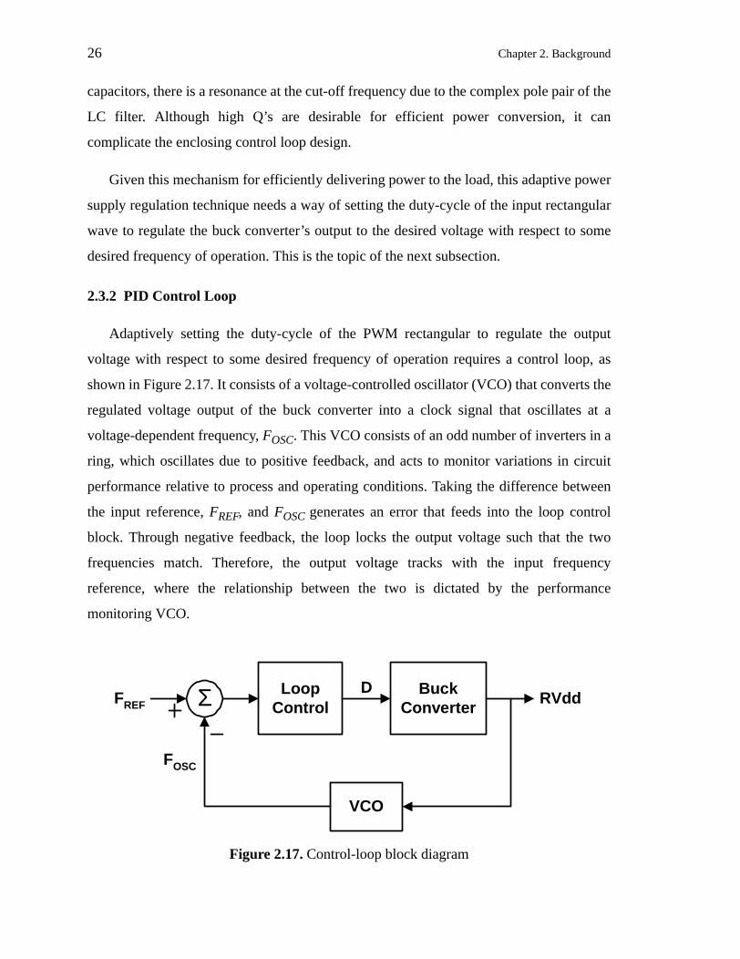
2.3.2 PID Control Loop
Adaptively setting the duty-cycle of the PWM rectangular to regulate the output
voltage with respect to some desired frequency of operation requires a control loop, as
shown in Figure 2.17. It consists of a voltage-controlled oscillator (VCO) that converts the
regulated voltage output of the buck converter into a clock signal that oscillates at a
voltage-dependent frequency, FOSC. This VCO consists of an odd number of inverters in a
ring, which oscillates due to positive feedback, and acts to monitor variations in circuit
performance relative to process and operating conditions. Taking the difference between
the input reference, FREF, and FOSC generates an error that feeds into the loop control
block. Through negative feedback, the loop locks the output voltage such that the two
frequencies match. Therefore, the output voltage tracks with the input frequency
reference, where the relationship between the two is dictated by the performance
monitoring VCO.
LoopControl
BuckConverter
VCO
Σ RVddFREF
D
FOSC
Figure 2.17. Control-loop block diagram

Chapter 2. Background 27
To achieve good transient response characteristics and stability without sacrificing
bandwidth, the loop uses proportional, integral, and derivative (PID) control. A
frequency-domain model of this PID loop is presented in Figure 2.18. The resulting
open-loop transfer function (loop gain) is as follows:
(2-10)
KP, KI, and KD set the pole and zero locations of the proportional, integral, and derivative
control block. KVCO represents the oscillator gain (Hz/V). Due to the time required to
perform the PID control calculations, its delay (T) through the loop causes additional
negative phase shift accounted for by the exponential term in the equation.
One difficulty associated with designing this type of controller arises from the
resonant peak in the frequency response of the buck converter. For simple integral control,
which consists of an integrator followed by the buck converter, there is a potential for
instability. An open-loop frequency analysis for this type of loop shows that if the
magnitude of the resonant peak crosses above the unity-gain magnitude, negative phase
shift due the integrator pole and a pair of poles from the LC filter eliminates phase margin.
Therefore, the integrator’s gain must be sufficiently low as to guarantee that the buck
converter’s resonant peak never crosses unity gain. Unfortunately, such a configuration
Σ
KP
sKD
KI/s Σ HLC(S)
KVCO
FREF
FOSC
RVdd
BuckConverterproportional
integral
derivative
Figure 2.18. PID control-loop frequency-domain model
Loop Gain HLCKVCO KP
KI
s----- sKD+ +
esTÐ
=

28 Chapter 2. Background
leads to low loop bandwidth and slow closed-loop transient response characteristics. To
combat this effect, adding a pair of zeros, utilizing proportional and derivative blocks, can
stabilize the loop without sacrificing bandwidth. Introducing the zeros at frequencies
below the cut-off frequency of the LC filter pushes unity gain crossing of the open-loop
response beyond the resonant peak and roles off at -20dB/dec. Furthermore, positive phase
shift from the zeros provides sufficient phase margin for a stable loop, as the magnitude
and phase response of the simulated open-loop transfer function in Figure 2.19
demonstrates. The bandwidth of the loop extends beyond what was achievable with
integral control alone and the resonant peak of the regulator LC is no longer a limiting
factor since it occurs below the unity gain frequency. In addition, because the bandwidth
exceeds the LC filter’s cut-off frequency, the loop can quickly respond to sudden load
transients that would otherwise perturb the output voltage. This fast response also prevents
other noise sources, such as sudden transients in the supply voltage to the buck converter,
from propagating to the output.
Implementation of the controller in Figure 2.17 relies on the ability to generate a PWM
rectangular wave, where the duty-cycle (D) is the value dictated by the output of a PID
control block. One possible approach would be to use a frequency detector that compares
103
104
-10
0
10
20
Mag
nitu
de(d
B)
103
104
-150
-100
-50
0
Pha
se(d
eg)
frequency (Hz)
Figure 2.19. PID control open-loop frequency response

Chapter 2. Background 29
the incoming reference clock with the output of the oscillator and generate an analog
voltage that corresponds to the frequency difference (or error). This error then drives the
PID control implemented with a set of amplifiers to generate an analog voltage that
corresponds to the desired output voltage. Translating this voltage to the appropriate
duty-cycle then relies on a comparator that compares a linear ramp wave that has a period
equal to the switching frequency of the buck converter to the PID control output. Figure
2.20 illustrates its operation. While the PID output is less than the ramp input, the output
of the comparator is low and goes high once the ramp exceeds the PID output. As a result,
changing the PID output proportionally changes the duty-cycle of the rectangular wave.
The enclosing feedback loop compensates for any offsets and non-linearities that may
exist in the translation.
Although this is a straight forward approach for implementing the PID control, it
requires several analog components that can be sensitive to supply and substrates noise
that exists in the targeted digital system. Also notice that the update rate of the buck
converter is set by its switching frequency. Therefore, the update of the control blocks can
occur at a rate much lower than the reference clock frequency. In addition, there is an
inherent analog-to-digital (A/D) conversion that occurs in the ring oscillator, which takes
an analog input voltage and generates a digital clock signal. Therefore, there is a potential
to build this controller consisting entirely of digital gates, and can be embedded along with
the rest of the digital system to which power is delivered. The issues and design of a
digital control loop are the topics of the next chapter.
VIN
DFigure 2.20. PWM rectangular wave generation

30 Chapter 2. Background
2.4 Summary
Power consumption in digital systems has been increasing at an accelerated rate and one
of the most effective ways to reduce unnecessary power consumption is to minimize the
overhead voltage normally required in fixed voltage designs by dynamically adjusting the
voltage to the minimum required for operation at a desired frequency. Given the quadratic
dependence on voltage, significant reduction in power consumption is possible and this
technique can enable more energy efficient operation for synchronous digital circuits.
The minimum supply voltage required with respect to frequency can be found by
using a ring oscillator that models the critical delay path in a synchronous digital system
and use negative feedback control to servo the output of an efficient switching regulator
[18]. Given the difficulty associated with generating an exact replica of the critical path, a
more flexible approach to modeling delay based on inverters is possible. This approach,
however, still requires some overhead margins to account for imperfect matching over a
wide range of supply voltages stemming from velocity saturation effects. The tracking
performance of the power supply regulator is set by the bandwidth of the control loop,
which can be improved with a PID control that guarantees stability without sacrificing
bandwidth. A PID loop has the added advantage that its bandwidth extends beyond the
cut-off frequency of the LC filter so that the loop can quickly respond to noise injected at
the output due to load transients. Although there are several approaches to designing this
adaptive supply voltage regulator, the following chapter describes a fully digital
implementation that fits well within a larger digital system.
31
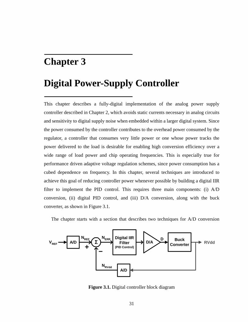
Chapter 3
Digital Power-Supply Controller
This chapter describes a fully-digital implementation of the analog power supply
controller described in Chapter 2, which avoids static currents necessary in analog circuits
and sensitivity to digital supply noise when embedded within a larger digital system. Since
the power consumed by the controller contributes to the overhead power consumed by the
regulator, a controller that consumes very little power or one whose power tracks the
power delivered to the load is desirable for enabling high conversion efficiency over a
wide range of load power and chip operating frequencies. This is especially true for
performance driven adaptive voltage regulation schemes, since power consumption has a
cubed dependence on frequency. In this chapter, several techniques are introduced to
achieve this goal of reducing controller power whenever possible by building a digital IIR
filter to implement the PID control. This requires three main components: (i) A/D
conversion, (ii) digital PID control, and (iii) D/A conversion, along with the buck
converter, as shown in Figure 3.1.
The chapter starts with a section that describes two techniques for A/D conversion
A/DNREF
NRVdd
BuckConverter RVdd
A/D
VREF ΣΣΣΣNERR
D/ADigital IIR
Filter(PID Control)
D
Figure 3.1. Digital controller block diagram

32 Chapter 3. Digital Power-Supply Controller
based on the inherent A/D property of a ring oscillator and then presents a discrete-time
sampled data implementation of the analog PID control blocks. The chapter continues
with a description of a variable-frequency controller which allows the digital controller to
operate with adaptive power supply regulation. Then, Section 3.3 presents a simpler and
lower power digital controller that operates at a fixed frequency, which has been
implemented to drive a low-power parallel link described in Chapter 4. An additional
advantage of building a fully-digital controller is the ease with which non-linear
techniques can be implemented to improve power conversion efficiency. These techniques
are described in Section 3.4.
3.1 A/D Conversion
A digital controller first requires the analog inputs and outputs of the system be converted
into digital signals in order to process them with digital functional units. As described in
Chapter 2, this adaptive supply-voltage regulation scheme uses the delay of inverters
(TINV) to model the critical path in the digital system and monitor how it reacts to process,
temperature, and voltage variations. A ring oscillator, consisting of an odd number of
inverters in a ring (nstages), performs a voltage-to-frequency conversion, where the
oscillation period is , since an edge traverses through the inverters in the
ring twice within a period. As illustrated in Figure 3.2, tapping out at a single point in the
ring and counting the digital clock signal over a fixed period of time performs a simple
A/D conversion. The binary output is a quantized representation of the voltage (VIN) that
depends on the counting interval (Tcount), with the following equation:
. (3-1)
2 nstages TINV⋅ ⋅
Counter NVIN
rst
FcountTINV
Figure 3.2. Ring oscillator and counter based A/D converter
NTcount
2 nstages TINV⋅ ⋅-----------------------------------------=

Chapter 3. Digital Power-Supply Controller 33
At the end of each interval, N is stored and the counter resets to zero for the subsequent
count. Fcount (= 1/Tcount) is set by the buck converter’s switching frequency. Since N
depends on Tcount and nstages, longer counting intervals and less inverter stages enable
higher resolution of the output. However, there is a limit and Tcount affects the
overall loop dynamics. It is important to count over the full period to obtain an average
magnitude of the power supply due to a small voltage ripple at the output of the buck
converter.
Since the performance of the counter can be measured as a function of inverter delays,
as long as its critical path is less than double the number of inverters in the ring, the
counter can also operate at the same voltage as the oscillator. In the case of a simple ripple
counter, only the first stage, implemented as a toggle flip-flop, sets the critical path since
subsequent stages operate at lower rates. Figure 3.3 illustrates the ring oscillator, ripple
counter, and finite state machine (FSM) used to implement this simple A/D converter [48].
The finite state machine not only resets the counter, but also allocates additional time at
the end of the counting interval, before the latching the output, to accommodate for the
worst-case ripple path through the counter. Assuming the clk-to-Q delay of a flip-flop is
on the order of 2-3 inverter delays, the worst-case ripple delay is set by the number of bits
nstages 3≥
Ringoscillator
(nstages)
T Qfosc
VIN
T Q
T Q
D Q
D Q
D Q
N[0]
N[1]
N[nbits]
Fcount
rst
rst
rst
FSM
Figure 3.3. A/D converter detailed schematic

34 Chapter 3. Digital Power-Supply Controller
in the counter (nbits) and the following equation:
. (3-2)
Hence, for the following inequality,
, (3-3)
the FSM must allow an additional ∆delay of time before latching the counter outputs. Since
the FSM enables the counter to operate at the same frequency and voltage as the ring
oscillator, the A/D converter’s power consumption tracks with the ring oscillator and
ultimately with the rest of the digital system to which power is supplied.
This simple approach to building an A/D converter can be improved by using phase
information to increase digital resolution of the analog voltage without a power penalty.
High switching frequency (for the buck converter) and high resolution are desirable for
building a digitally controlled regulator with good performance. Higher switching
frequencies enable higher bandwidths for the control loop and higher resolution
minimizes quantization error that results from a digital implementation of an inherently
analog loop. Given a target switching frequency of 1-MHz and 10 bits of resolution, a
simple ring oscillator and counter used for A/D conversion must run at an extremely high
rate. Since the least significant bit (LSB) corresponds to a single oscillator cycle, to
convert the maximum voltage to the maximum digital output of the counter, the counter
must run at 1-GHz. This leads to significant power consumption in the A/D conversion
block which increases overhead power and degrades the converter efficiency. Instead,
reducing the LSB to a fraction of the oscillation period is preferable.
To lower the A/D converter’s power consumption, an improved version based on a
technique that relies on a delay-line instead of a ring oscillator [8] is presented in Figure
3.4. In this implementation, the ring oscillator and counter structure is retained for
hardware reuse and to avoid the geometrically increasing number of delay stages with
each additional bit of resolution. The counter output now only accounts for the five higher
order bits, N[9:5], of the digital output. Similar to the original approach, the counter
counts pulses out of the ring oscillator over the switching period of the buck converter, but
Worst-case ripple path 3nbits TINV⋅=
∆delay 3nbits TINV⋅ 2nstages TINV⋅Ð 0>=

Chapter 3. Digital Power-Supply Controller 35
generates a course grain representation of the input voltage. The lower order bits of
resolution are extracted from the delay line. Instead of a just implementing a delay line
consisting of inverters, each delay element consists of a static pass transistor latch that
captures the internal state of the ring at the end of the counting period. A synthesized
encoder takes the output of each of the 32 delay stages and determines how far an edge has
traversed through the ring to generate the lower order bits, N[4:0], of the binary
representation of the input voltage. NAND gates reset the ring in order to have it restart
from a known initial state. This approach reduces the LSB of the A/D converter from an
entire oscillation period to a single delay stage and reduces the counter’s power
consumption. So, while the previous design would require a 1-GHz oscillator for 10 bits
of resolution at a switching period of 1-MHz, the oscillator in the new implementation
only needs to oscillate at 32-MHz for the same resolution and switching frequency. It is
important to point out here that this approach does not reduce the ring oscillator’s power
since it is set the by total switched capacitance and inverter delay, and not the oscillation
frequency. Since the additional cost of the encoder block is small, this implementation
enables low-power solution.
The A/D conversion techniques described thus far have been used to convert the
output of the buck converter into a frequency and then into an equivalent digital
representation of the voltage and frequency. Comparing this value to a reference
determines whether the buck converter output voltage corresponds to the value required
for the digital system to operate at the desired frequency of operation. If the reference is a
Counter
Encoder
N[9:5]
N[4:0]
VIN
rststart
Figure 3.4. Low-power A/D converter

36 Chapter 3. Digital Power-Supply Controller
voltage, the difference between the outputs of two A/D blocks with the same counting
interval generates a binary equivalent of the voltage difference. Good matching between
the two oscillators ensures the regulated voltage matches the reference voltage. Given a
frequency-locked loop, as described in Chapter 2, which assumes the reference is a clock
frequency, the reference clock would feed straight into the counter and bypass the ring
oscillator in the reference A/D path. In this case, the oscillator in the feedback path of the
regulator must accurately model the critical path of the digital system to which power is
delivered.
Given a digital representation of the difference between the regulated voltage and the
reference, this error must then drive PID control blocks to servo the duty-cycle of the
PWM rectangular wave to the buck converter, and drive the error to zero through negative
feedback. A digital circuit equivalent of the PID control that operates on the error is
covered next.
3.2 Digital PID Control
This section describes the digital implementation of the PID controller [49] that operates
on the error generated by the A/D converters described above. Separate digital blocks
implement the discrete-time equivalents of the proportional, integral and derivative
functions of the controller. The output sum, yPID, is a binary representation of the
duty-cycle of the PWM rectangular wave that drives the buck converter. These digital
blocks implement the following discrete-time functions:
(3-4)
(3-5)
(3-6)
. (3-7)
x(n) represents the feedback error between the regulated output voltage and the reference
at each discrete-time n. Each discrete interval n is equivalent to the switching period of the
yP n( ) kP x n( )⋅=
yI n( ) yI n 1Ð( ) 1kI----x n( )+=
yD n( ) kD x n( ) x n 1Ð( )Ð[ ]=
yPID n( ) yP n( ) yI yD n( )+ +=

Chapter 3. Digital Power-Supply Controller 37
buck converter and control signals are pipelined through the digital blocks at this rate. The
resulting discrete-time equivalents of the PID control blocks closely mimic the
continuous-time transfer function, described in Chapter 2.
Detailed block diagrams of the three control blocks are presented in Figure 3.5. Since
the update rate of the digital control is significantly lower than the rest of the digital
system to which power is regulated, it has low performance requirements. Therefore,
discrete-time control blocks utilize simple ripple-carry adders for addition and subtraction.
Binary shifters implement multiplication and division, but limits multiplication and
division to powers of 2, as follows:
, (3-8)
where Nshift corresponds to the binary shift amount with negative values corresponding to
division by shifting right (e.g. 2-2 = 1/4). Proportional control is a simple multiplication by
kD. Integral control is equivalent to accumulation in the digital domain and requires a
register to store the output from the previous cycle (n-1) and add a fraction of the error, set
by constant kI, in the current cycle. In order to avoid quantization effects that can result
from shifting, all lower order bits are preserved for the calculations. Lastly, the derivative
function takes a difference between the current and previous cycle’s error values, and
Σx(n) yPID(n)Σ
Σ = 2-input adder
= binary shifter
Z-1 = register
Σ
Z-11/kI
kP
Z-1
ΣkD
Figure 3.5. Circuit implementation of PID control blocks
k 2Nshift=

38 Chapter 3. Digital Power-Supply Controller
multiplies it by a constant kD. An output sum of these blocks result in the desired PID
control and corresponds to a binary equivalent of the required duty-cycle D input to the
buck converter.
Minimum device sizes reduce controller energy consumption at the expense of slower
operation. This slow performance is acceptable in this case because of its relatively low
update rate. Furthermore, its low performance requirements allow all the PID control logic
to operate off of the regulated supply voltage. Therefore, both A/D converter blocks and
the PID control, described so far, also benefit from the power savings provided by
adaptive power-supply regulation and their power consumption tracks with the load. If the
rest of the controller, namely the D/A converter and buck converter, can also operate off of
the regulated voltage, the controller’s total power can always be a fixed percentage of the
power delivered and maintain high conversion efficiency across a wide range of regulated
voltage levels. Unfortunately, this may not always be possible and power consumed in the
D/A converter and buffers required to drive the buck converter can limit converter
efficiency.
Inefficiencies in the overall regulator stem from three main sources of overhead
power. While losses due to switching transistor resistance tracks with load current, the
ramp-up buffer chain to drive these large switches consumes a relatively fixed amount of
power to drive a fixed capacitive load. Lastly, the D/A converter consumes overhead
power and can vary depending on its implementation. Efficiency is measured as a ratio of
the power delivered to the load versus the total power consumed by the regulator, defined
by the following equation:
. (3-9)
Pload varies depending on the requirements of the system being driven and affects
conversion efficiency. For high load power requirements, power consumed by the
controller can be a small fraction such that efficiency is dominated by the buck converter
and load. However, for low power conditions, the controller’s power can be significant
and the dominant factor that limits conversion efficiency.
Converter EfficiencyPload
Pload Pdriver Pbuck Pcontroller+ + +------------------------------------------------------------------------------------------=

Chapter 3. Digital Power-Supply Controller 39
The loop’s update rate (or switching frequency), designated as Floop, clocks the digital
controller and sets the time base for the overall regulator system. A sampled average of the
buck converter output voltage and input reference are found during a single Floop cycle as
well as the PID calculations. A subsequent D/A block operating over the same period
translates the digital PID control output to a PWM rectangular wave. Given that the error
sampling and update occur at the loop frequency, the PID control time constants are
proportional to Floop. The cut-off frequency of the LC filter in the buck converter,
however, is fixed and independent of Floop. In order to maintain a stable control loop over
a dynamic range of regulated voltage levels, a fixed loop frequency is necessary to
guarantee a fixed relationship between the loop parameters of the PID control and buck
converter. The most obvious approach is to use a fixed-frequency controller.
Unfortunately, such an implementation can result in considerable overhead power
consumed by the D/A block that doesn’t track with the regulated voltage and power
delivered to the load. A breakdown of the power consumed by an initial implementation of
a fixed-frequency controller briefly described in the following subsection motivates a
variable-frequency controller design that is described next.
3.3 Variable-Frequency Control
Whether the loop is a fixed- or variable-frequency controller is determined by the
implementation of the D/A conversion. Figure 3.6 presents a block diagram of the overall
coun
ter
coun
ter
FREF Digital PID
(binary adders and
shifters)
NREF
systemcounter
NOSC
NDUTY
FSYS
buckconverter
VCO
RVdd
FOSC
fixed: 9variable: 7~10FSWITCHING
Figure 3.6. Digital PID control loop

40 Chapter 3. Digital Power-Supply Controller
power-supply regulator loop. D/A conversion is achieved by taking the output of the
digital PID controller and comparing it to a binary ramp wave generated by a free-running
synchronous counter. This is a digital equivalent of the analog PWM rectangular wave
generator described in Chapter 2. The monotonically increasing binary ramp repeats at a
rate set by the input clock, Fsys, and the number of bits in the counter, Nramp. This rate
corresponds to the update rate of the controller and set by the following equation:
. (3-10)
Waveforms in the inset box in Figure 3.6 illustrates the generation of the variable
duty-cycle rectangular wave that drives the buck converter. The conversion is governed by
the a linear relationship between yPID and the duty cycle as follows:
, (3-11)
where Nmax corresponds to the maximum count value of the synchronous counter and has
the same number of bits as yPID. The ramp wave’s period sets the period of the rectangular
waveform. A binary comparator, implemented with only the carry portion of a subtractor,
takes the difference between the PID output and the binary ramp, and looks at the carry
output of the highest order bit. At the beginning of the comparison, the binary ramp starts
lower than the PID output and the carry out is low. Once the binary ramp exceeds the PID
output, the highest order carry bit flips high and this transition corresponds to the
appropriate pulse-width set by the PID control. The overall feedback loop constantly
updates the PID output to proportionally modulate the duty-cycle of the rectangular wave
input to the buck converter.
In a fixed-frequency implementation, Fsys is a fixed-frequency clock and generates a
fixed update rate, Floop, for the controller. This constraint requires the counter for the D/A
conversion to be operated at a fixed rate and a fixed voltage, and as a result, is the
dominant source of overhead power dissipation. To highlight the inefficiencies stemming
from this overhead, Figure 3.7 presents a distribution of the measured power consumed by
a power supply regulator, fabricated in a MOSIS 1.2µm CMOS technology [48], at three
different voltages regulated down from 5-V. The bar graph presents the percentage of the
Floop
Fsys
max Nramp( )-------------------------------=
Duty cycleyPID
max Nramp( )-------------------------------=

Chapter 3. Digital Power-Supply Controller 41
power consumed by different parts of the regulator and the power delivered to a resistor
load relative to the total identified on the top of each bar. The controller’s power,
dominated by the D/A converter, increases as a percentage of the total to degrade
converter efficiency as voltage reduces. To make matters worse, dynamic power of typical
digital circuits is proportional to V3, while a resistor’s power is proportional to V2.
Therefore, application to an actual digital load would result in even lower conversion
efficiencies.
The key to improving conversion efficiency while maintaining loop stability is to
allow the internal frequency and voltage of the controller to change while keeping the
controller’s loop parameters relatively constant [49]. Since these parameters are
proportional to the update rate (or loop frequency) of the controller, Floop must remain
relatively constant (within a factor of two). In the previous design, the buck converter’s
switching frequency corresponds to the frequency of the binary ramp wave generated by
the synchronous counter, which was clocked by an external fixed-frequency system clock.
In a variable loop-frequency scheme, this system counter is clocked by the ring oscillator
driven by the regulated voltage or the reference, and the number of counter bits varies
depending on its region of operation. To accomplish this, a frequency detection circuit is
required. A new system counter has a maximum count (max(Nramp)) ranging from 128 to
1024 (7 to 10 bits), determined by a frequency-detect circuit and a variable-frequency
Figure 3.7. Normalized power breakdown
4V 3V 2V
92.1%
100%
RVdd
81.9%
88.8%
90%
80%
0.61% 1.03%2.10%
3.95%
5.27%
2.76%
4.55% 6.56%
9.44%
Buck Conv.Driver
ControllerLoad
Per
cen
tag
eo
fTo
talP
ow
er
1.13 W 0.70 W 0.34 W
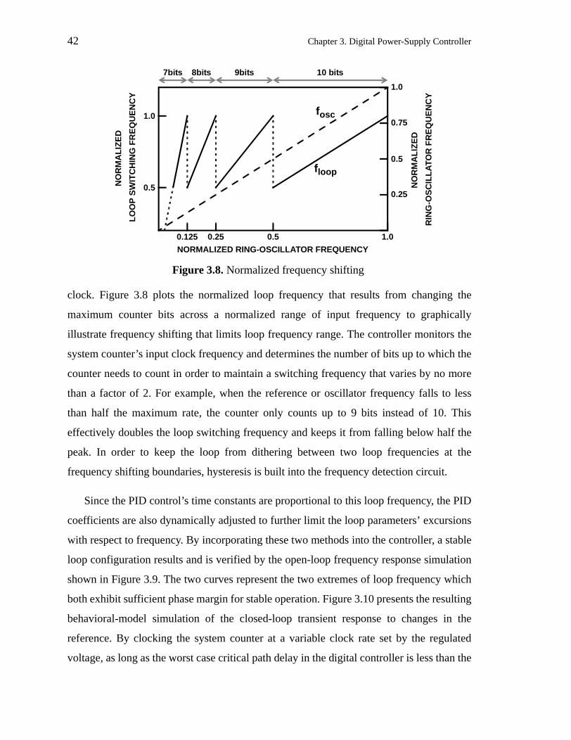
42 Chapter 3. Digital Power-Supply Controller
clock. Figure 3.8 plots the normalized loop frequency that results from changing the
maximum counter bits across a normalized range of input frequency to graphically
illustrate frequency shifting that limits loop frequency range. The controller monitors the
system counter’s input clock frequency and determines the number of bits up to which the
counter needs to count in order to maintain a switching frequency that varies by no more
than a factor of 2. For example, when the reference or oscillator frequency falls to less
than half the maximum rate, the counter only counts up to 9 bits instead of 10. This
effectively doubles the loop switching frequency and keeps it from falling below half the
peak. In order to keep the loop from dithering between two loop frequencies at the
frequency shifting boundaries, hysteresis is built into the frequency detection circuit.
Since the PID control’s time constants are proportional to this loop frequency, the PID
coefficients are also dynamically adjusted to further limit the loop parameters’ excursions
with respect to frequency. By incorporating these two methods into the controller, a stable
loop configuration results and is verified by the open-loop frequency response simulation
shown in Figure 3.9. The two curves represent the two extremes of loop frequency which
both exhibit sufficient phase margin for stable operation. Figure 3.10 presents the resulting
behavioral-model simulation of the closed-loop transient response to changes in the
reference. By clocking the system counter at a variable clock rate set by the regulated
voltage, as long as the worst case critical path delay in the digital controller is less than the
Figure 3.8. Normalized frequency shifting
NO
RM
AL
IZE
D
NORMALIZED RING-OSCILLATOR FREQUENCY
fosc
1.0
0.75
0.25
1.0
0.5
0.5
floop
NO
RM
AL
IZE
D
0.50.250.125 1.0
10 bits9bits8bits7bits
RIN
G-O
SC
ILL
ATO
RF
RE
QU
EN
CY
LO
OP
SW
ITC
HIN
GF
RE
QU
EN
CY
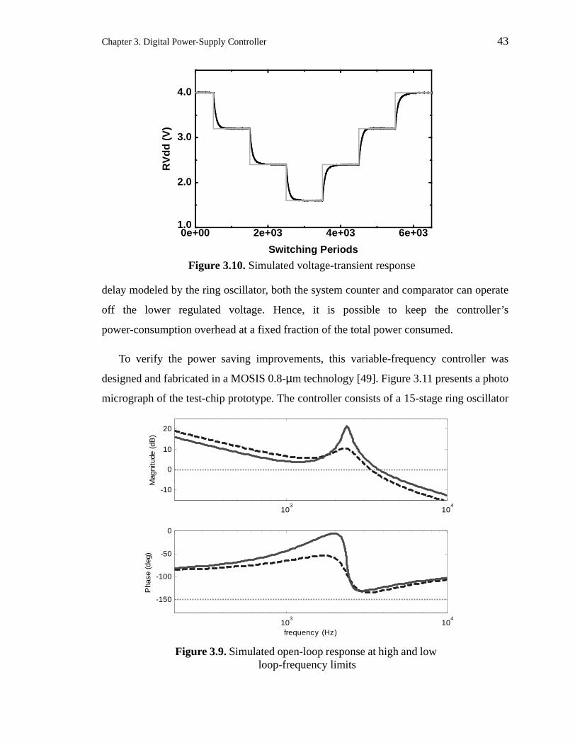
Chapter 3. Digital Power-Supply Controller 43
delay modeled by the ring oscillator, both the system counter and comparator can operate
off the lower regulated voltage. Hence, it is possible to keep the controller’s
power-consumption overhead at a fixed fraction of the total power consumed.
To verify the power saving improvements, this variable-frequency controller was
designed and fabricated in a MOSIS 0.8-µm technology [49]. Figure 3.11 presents a photo
micrograph of the test-chip prototype. The controller consists of a 15-stage ring oscillator
103
104
-10
0
10
20
Mag
nitu
de(d
B)
103
104
-150
-100
-50
0
Pha
se(d
eg)
frequency (Hz)
Figure 3.9. Simulated open-loop response at high and lowloop-frequency limits
Figure 3.10. Simulated voltage-transient response
0e+00 2e+03 4e+03 6e+03
Switching Periods
1.0
2.0
3.0
4.0
RV
dd
(V)

44 Chapter 3. Digital Power-Supply Controller
that oscillates at a peak frequency of 116-MHz at 5-V and the loop frequency ranges from
57-114 kHz. The switching transistors for the buck converter are shown on-chip. The
converter’s external LC filter components are 70-µH and 70-µF and regulate down from a
5-V external supply. Figure 3.12 plots the measured power for the digital controller and
buffers that drive the large on-chip switching transistors across a wide range of regulated
Figure 3.11. Test-chip micrograph
Figure 3.12. Overhead power vs. regulated voltage
0
5
10
15
20
25
30
35
40
45
1.5 2 2.5 3 3.5 4 4.5
Po
wer
(mW
)
Regulated voltage RVdd (V)
Digital Controller
Power Xtor Driver

Chapter 3. Digital Power-Supply Controller 45
voltages. Since the digital controller powers off the regulated supply, its power
consumption exhibits the same cubed dependence on voltage as the dynamic power of
synchronous digital circuits that load the regulator. Buffers that drive the buck converter
switches, however, must operate off a fixed supply and so its power doesn’t track with
regulated voltage. Instead, variations in this power is governed by the variable loop
frequency and other non-linear low-power techniques described in Section 3.5. Now that
the controller is no longer a dominant source of overhead power at lower voltages,
conversion efficiency significantly improves for lower supply voltages as demonstrated by
the measured converter efficiency versus regulated voltage plotted in Figure 3.13. The
regulator targets a synchronous digital logic chip that consumes 1-W at 4-V, and its
dynamic power is proportional to V3 as shown by the dotted line with its corresponding
magnitudes specified on the right axis.
While conversion efficiency is an important measure of regulator performance, good
transient response characteristics are also desirable. There are two aspects of the
regulator’s transient response that must be evaluated. An important characteristic for all
power supply regulators is its response to sudden changes in the load. As described in
Section 2.2, PID control extends the loop bandwidth to exceed the LC cutoff frequency of
the filter. Since load variation perturbs the regulator output voltage at a time constant set
by the resonant frequency of the filter, the higher bandwidth allows the loop to quickly
Figure 3.13. Conversion efficiency vs. regulated voltage
1.5 2 2.5 3 3.5 4
Eff
icie
ncy
(%)
Regulated voltage RVdd (V)
0
200
400
600
800
1000
1200
1400
Lo
adP
ow
er(m
W)
75
80
85
90
95
100

46 Chapter 3. Digital Power-Supply Controller
correct for load variations. Figure 3.14 plots data extracted from a digital sampling
oscilloscope to demonstrate the loop’s ability respond to both increasing and decreasing
step changes in load current; where the dotted lines delineate step changes in load current
between 0-mA and 100-mA at 4-V. The output varies by less than 2-% of the regulated
voltage level and settles within 200-µs. In order to enable a digital system that can adapt
its operating frequency depending on performance needs, this regulator must also quickly
adapt its voltage to the needs of different frequencies. The rate at which this power supply
regulator can change its voltage is set by the bandwidth of the loop. Figure 3.15 presents
the loop’s output voltage-transient response which tracks rising and falling step changes in
the reference. Due to a loop frequency shifting boundary that exists halfway through the
Figure 3.14. Measured load transient response
3.95
4
4.05
4.1
4.15
3.9
3.95
4
4.05
4.1 100µs
Figure 3.15. Measured voltage transient response
2ms
1VVREF
RVdd

Chapter 3. Digital Power-Supply Controller 47
voltage transient, the loop’s bandwidth also changes halfway through the falling transition
and therefore results in slightly different bandwidths for the rising and falling transitions.
Enabling variable frequency operation results in a controller whose power tracks with
the variable frequency and regulated voltage such that its power consumption is a fixed
fraction of the CV2f power consumed in the load. However, this approach still suffers
from high power consumption at high frequencies and voltages, limiting its efficiency for
low-power loads. A digital controller requires blocks that digitize voltage and time into
discrete increments. The two iterations described so far rely on a ring oscillator and
counter for digitizing operations. And digitalization that relies on a ring oscillator results
in the least significant bit (LSB) equivalent to an oscillation period. Therefore, in order to
achieve high resolution and high buck converter switching frequencies, the ring oscillator
and counter must run at a high rate. A 1-MHz switching frequency and 9-bit resolution
requires a maximum rate on the order of 500-MHz. Higher resolution requires even higher
oscillation frequencies. The ring oscillator does not have to exactly match the critical path
since some gain factor can be used in the loop to account for the differences, but the higher
frequency stresses the performance of the counter and leads to higher power consumption.
However, an implementation that relies on a delay line, rather than a ring oscillator, can
leverage more timing information that is available within the delay line for higher
resolution. A technique that builds on this ability to obtain higher resolution can lower the
overall power consumption of the controller, eliminate the complexity required for
variable frequency operation, and is described next.
3.4 Low-Power Control
A digital controller design that utilizes a tapped delay-line to implement an effective D/A
conversion with low overhead was demonstrated in [6]. In this implementation, the total
delay through the delay-line matches the switching period and a digital number taps out
the fractional delay that corresponds to the desired pulse width. So, it reduces power
consumption by obviating the need for a highly active system counter and comparator
operating at high frequencies. To address the high power consumption in the digital
controller that limits conversion efficiency, a low-power implementation that utilizes a

48 Chapter 3. Digital Power-Supply Controller
low-power A/D converter, described in Section 3.1, and a subsequent D/A block that also
leverages a delay line is described. It relaxes the need for higher frequency operation in
the D/A block and reduces its LSB to a few gate delays.
This lower power controller relies on a D/A that taps out at discrete points along a
delay line and uses this additional timing information to reduce the LSB to a fraction of
the oscillation period. A detailed block diagram of the improved D/A blocks, presented in
Figure 3.16, generates a fixed frequency PWM rectangular wave whose pulse width is set
by the digital output of the PID block denoted as D[9:0]. A ring oscillator consisting of
several delay stages operates off of a fixed voltage to generate fixed frequency pulses to a
counter. However, a single period is no longer the LSB and therefore allows much slower
oscillation periods to reduce the frequency of operation for the counter. At the beginning
of the switching cycle, the counter is reset to zero and a comparator waits until the counter
output matches the five higher order bits of D[9:4]. Once there is match, it triggers the
control to latch an edge of out the multiplexor. The multiplexor chooses a point along the
ring which has a delay that corresponds to the number of buffer stages set by the four
lower order bits of D[3:0]. Therefore, the LSB is reduced to the delay of a single buffer
stage as opposed to a complete oscillation period. This implementation retains the ring
oscillator and counter structure to reuse hardware and avoid a large delay line that can
result in order to implement a large number of bits for high resolution. The counter
mux
Vdd
control
counter/comparator
PWM
[3:0]
[9:4]Duty[9:0]
rst
start
Figure 3.16. Low-power D/A block diagram

Chapter 3. Digital Power-Supply Controller 49
continues to count pulses out of the oscillator until the counter reaches its maximum count
which denotes the end of the switching period.
The ring-oscillator frequency and counter set the switching period (or Floop). Given a
5-bit counter, there are 32 ring-oscillator cycles in the switching period and thus requires
the ring to oscillate at 32-MHz for a 1-MHz PWM rectangular wave. The ring consists of
16 delay stages to generate the finer delay granularity set by the four lower order bits.
Each delay stage consists of a NAND gate, as shown in the inset box in Figure 3.16, in
order to restart the ring at the beginning of each switching period from a known state.
Since this ring must operate at a fixed frequency, it operates off of a fixed supply voltage.
The external high supply of the buck converter is used and the delay of each stage is
designed to be approximately 1ns for an oscillation frequency of 32-MHz. Since the
performance requirements of the counter is now much lower, the other components of the
D/A conversion block operates off the regulated supply so that it dissipates less power.
Figure 3.17 presents the overall block diagram of this improved digital controller for
adaptive supply regulation. Low-power A/D blocks that consist of tapped ring oscillators
convert the reference and regulated voltages to binary equivalents to generate a feedback
error. A discrete-time digital implementation of the PID control operate on the error to
generate a binary equivalent of the duty-cycle for the buck converter. The low-power D/A
block which also consists of a tapped ring oscillator converts the binary PID output into a
PWM rectangular wave. This block also generates the 1-MHz update rate for the PID
In = In-1 + en/kI
en
Pn = kpen
Dn = kD(en-en-1)
Low-powerA/D
Low-powerA/DVCTRL
buckconverter
Duty[9:0]
RVdd
Low-powerD/A
Σ
PWM
Figure 3.17. Low-power controller block diagram

50 Chapter 3. Digital Power-Supply Controller
control blocks and counting interval of the A/D converter blocks. Except for the
fixed-frequency ring oscillator in the D/A block and the buck converter, all digital
components in this controller operate off a lower regulated supply in order to reduce
power consumption. A simple low-to-high swing converter, shown in Figure 3.18, is used
to interface the lower voltage blocks to the high voltage buffers that drive the buck
converter.
This digital power supply controller was implemented within a high-speed I/O
interface chip in order to offer the power savings possible with adaptive supply voltage
regulation. A DLL in the I/O interface generates the reference voltage, which sets the
desired regulator voltage output. A zoomed-in photo micrograph of the power supply
prototype fabricated in a HP0.35-µm CMOS technology [50] is presented in Figure 3.19.
On-chip switching transistors for the buck converter operate off a 3.3-V external supply
and have maximum widths of 7-mm and 3.5-mm for the pMOS and nMOS devices,
respectively. These sizes are optimized to drive 250-mW of peak load with a switching
frequency of 1-MHz. nMOS gate capacitors fill empty die space to reduce power supply
noise that can result from large current switching transients. The external filter inductor
and capacitor are 10-µH and 10-µF, respectively. The digital controller’s overhead power
is 1.5-mW while regulating 2.7-V, and converter efficiency is greater than 90-% while
delivering 200-mW. This overhead, considerably less than that achieved in previous
IN
OUTIN
RVdd RVdd
Vdd
Figure 3.18. Low-to-high voltage converter

Chapter 3. Digital Power-Supply Controller 51
implementations, is possible through the low-power A/D and D/A blocks. The measured
regulator voltage range is limited by a lower range limit in the I/O implementation and is
1.3-3.2 V. Converter efficiencies greater than 80-% is achieved for this range with
delivered load power ranging from 50-mW to 300-mW.
3.5 Non-Linear Power Reduction Techniques
One of the advantages of a completely digital, discrete-time implementation of the power
supply controller is the ability to easily incorporate non-linear techniques in efforts to
improve converter efficiency [6],[45],[48]. The previous sections described various
techniques to reduce power consumption in the digital implementation of a linear PID
control. This section describes techniques to reduce two dominant components of loss in
the buck converter: (i) resistive loss through the transistor switches and (ii) switching loss
needed to drive the switching transistors. An equation to optimally size the switching
transistor that trade-off these two loss components is a function of load power. Over a
wide operating range, however, this optimum changes due to the load power’s strong
dependence on its operating frequency. Therefore, dynamically reducing transistor sizes
close to the optimum under lower load conditions leads to higher conversion efficiencies
Figure 3.19. Power-supply controller block photo micrograph (zoom)
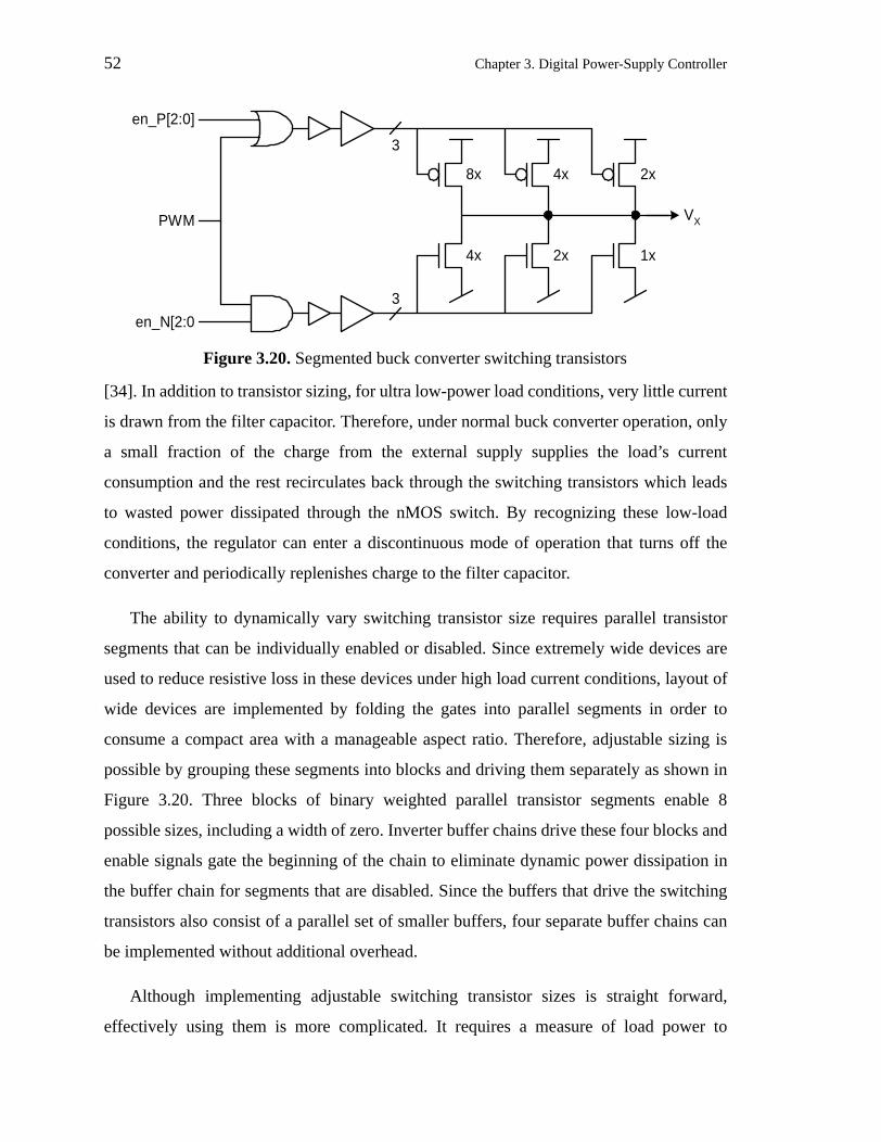
52 Chapter 3. Digital Power-Supply Controller
[34]. In addition to transistor sizing, for ultra low-power load conditions, very little current
is drawn from the filter capacitor. Therefore, under normal buck converter operation, only
a small fraction of the charge from the external supply supplies the load’s current
consumption and the rest recirculates back through the switching transistors which leads
to wasted power dissipated through the nMOS switch. By recognizing these low-load
conditions, the regulator can enter a discontinuous mode of operation that turns off the
converter and periodically replenishes charge to the filter capacitor.
The ability to dynamically vary switching transistor size requires parallel transistor
segments that can be individually enabled or disabled. Since extremely wide devices are
used to reduce resistive loss in these devices under high load current conditions, layout of
wide devices are implemented by folding the gates into parallel segments in order to
consume a compact area with a manageable aspect ratio. Therefore, adjustable sizing is
possible by grouping these segments into blocks and driving them separately as shown in
Figure 3.20. Three blocks of binary weighted parallel transistor segments enable 8
possible sizes, including a width of zero. Inverter buffer chains drive these four blocks and
enable signals gate the beginning of the chain to eliminate dynamic power dissipation in
the buffer chain for segments that are disabled. Since the buffers that drive the switching
transistors also consist of a parallel set of smaller buffers, four separate buffer chains can
be implemented without additional overhead.
Although implementing adjustable switching transistor sizes is straight forward,
effectively using them is more complicated. It requires a measure of load power to
1x
2x
2x
4x
4x
8x
3
3
en_P[2:0]
en_N[2:0
PWM VX
Figure 3.20. Segmented buck converter switching transistors

Chapter 3. Digital Power-Supply Controller 53
appropriately size them. The power supply regulator can leverage the dynamic power
equation, which has a cubed dependence on voltage. The regulated output voltage can be
determined by looking at the output of the PID control and used to set the appropriate
width. This simple approach assumes the activity of the load is a nominally fixed value.
Unfortunately, power saving techniques, such as clock gating, can cause significant
fluctuations in circuit activity for the same voltage. Additional information provided by
the system is therefore required to compensate for these differences in power requirements
of the load. Alternatively, a current sensor that monitors the average current delivered to
the load may provide the necessary information to set optimal transistor widths.
While there is a strong correlation between voltage and power consumption, dynamic
power can also vary with respect to switching activity. Therefore, a condition may arise
that requires a high voltage to enable fast operation for a small segment of a chip, while
the rest of the system is inactive. This can result in a condition where the buck converter
dissipates power through recirculating current, because the average current delivered to
the load is less than half the ripple current amplitude. Recirculating current can be avoided
by sensing when recirculating current occurs and then disabling subsequent pulses to the
buck converter until the output falls below a preset threshold. Once a voltage droop is
detected, the controller sends discrete packets of charge until the output magnitude is
restored. This discontinuous operation still requires the front-end of the controller to
remain active to sense the voltage error, but, it reduces the buck converter switching losses
by reducing switching activity and removing recirculating currents. The mechanism for
detecting when recirculating current occurs uses a voltage detector illustrated in Figure
3.21. At the end of the switching period, both pMOS and nMOS devices are briefly turned
off and the drain voltage is sampled. In the case of recirculating current, the current
magnitude through the inductor is negative and therefore charges up the drain capacitor. A
fast precharged inverter senses whether the drain voltage rises above a threshold voltage
and drives a series of meta-stability hardened flip-flops. Detecting when there is
recirculating enables the controller to operate in a discontinuous mode that periodically
send packets of charge to supply the low currents consumed by the load and otherwise
minimizes resistive losses through the buck converter.

54 Chapter 3. Digital Power-Supply Controller
3.6 Summary
Implementing the power supply controller entirely out of digital gates offers several
advantages. Since this adaptive power supply regulation scheme targets large digital
systems to optimize its energy consumption, a digital implementation can be embedded
within the same die and does not require the special attention normally required for
mix-signal designs. It results in a simpler and robust design that may be synthesized and is
portable. Furthermore, a digital implementation can leverage the same power saving
technique enabled by the regulator such that its power consumption tracks with the
frequency of operation. Lastly, a digital implementation allows non-linear techniques that
can reduce losses and improve converter efficiency.
This chapter described three iterations of the digital controller, where each iteration
reduces the overhead power consumption of the controller to improve power conversion
efficiency. An approach that relies on a simple ring oscillator and counter for A/D and
D/A conversion is effective, but high switching activity and operation off of a fixed high
VX
D Q D Q
sense
detect
clk
Cjd
RVdd
VX
buck converterIL
Figure 3.21. Recirculating current detector

Chapter 3. Digital Power-Supply Controller 55
supply voltage results in significant overhead power dissipation and low converter
efficiency. A variable-frequency controller improves the design and enables the controller
power to track with the load, but high switching activity in the D/A block still limits its
use for low-power loads. A new approach that removes the high switching activity without
sacrificing resolution yields a much more viable solution for low load-power applications.
Another digital controller that utilizes a non-linear sliding window control scheme also
has been developed to further improve converter efficiency for low-power digital
applications [25].
The low-power controller described in this chapter has been implemented along with
an I/O subsystem to adaptively regulate the voltage to a low-power parallel interface. By
using feedback to lock the regulated voltage with respect to an input reference, the
regulated voltage contains information about the process and environmental conditions.
This information can be leveraged by the circuits in the I/O subsystem to replace precision
analog circuits with simple digital gates that now have precise delays with respect to
frequency. Chapter 4 describes how an adaptively regulated power supply environment
enables a simple and robust I/O interface and the power savings it offers.

56 Chapter 3. Digital Power-Supply Controller

57
Chapter 4
I/O Interface Design
High performance point-to-point parallel interfaces have become increasingly important.
They are used in driving flat panel displays [13], communication between
microprocessors in parallel machines [37], processor to memories [55], graphics
subsystems and peripherals [21], and for enabling high bandwidth communication in
high-speed network devices [14]. This chapter describes how adaptive power supply
regulation can be applied to a high-speed parallel I/O interface implementation to reduce
its power consumption. Furthermore, dynamically scaling supply voltage with respect to
operating frequency also offers several advantages the link designer can leverage to build
a simple and yet robust interface.
Building a supply adjusted parallel I/O interface requires the same set of components
found in conventional parallel links, with the addition of an adaptive power supply
regulator. Section 4.1 begins with an overview of a parallel data interface, presents the
critical path that limits the peak clock rates achievable, discusses signal integrity issues
that affect high performance links, and highlights potential advantages of operating off of
an adaptively regulated power supply. One of these potential advantages is the ability to
maximize energy efficient operation, which requires that the critical path delay in the I/O
subsystem must be known in order to optimally regulate the supply voltage. Section 4.2
describes a core DLL design that generates the “right” (optimal) voltage of operation
relative to the critical path in the I/O subsystem in addition to providing multiple equally
spaced clock phases to the timing recovery block. Section 4.3 then presents a
current-mode transmitter and describes how adaptively regulating the supply voltage
affects its operation and performance. The subsequent section then describes a receiver
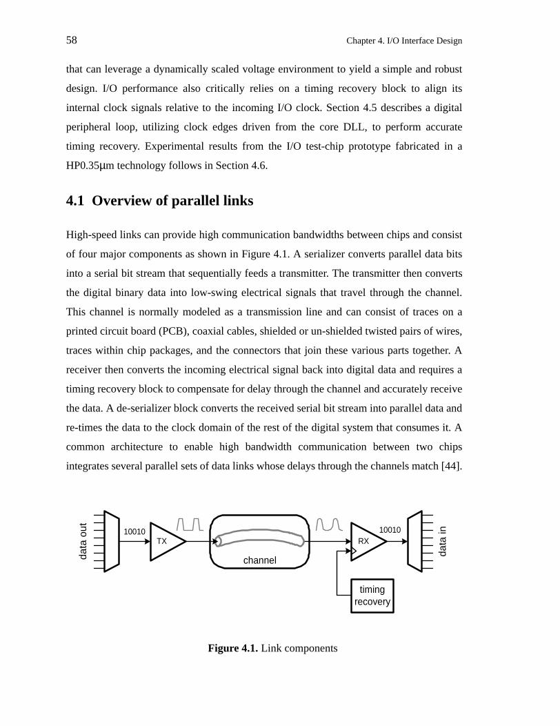
58 Chapter 4. I/O Interface Design
that can leverage a dynamically scaled voltage environment to yield a simple and robust
design. I/O performance also critically relies on a timing recovery block to align its
internal clock signals relative to the incoming I/O clock. Section 4.5 describes a digital
peripheral loop, utilizing clock edges driven from the core DLL, to perform accurate
timing recovery. Experimental results from the I/O test-chip prototype fabricated in a
HP0.35µm technology follows in Section 4.6.
4.1 Overview of parallel links
High-speed links can provide high communication bandwidths between chips and consist
of four major components as shown in Figure 4.1. A serializer converts parallel data bits
into a serial bit stream that sequentially feeds a transmitter. The transmitter then converts
the digital binary data into low-swing electrical signals that travel through the channel.
This channel is normally modeled as a transmission line and can consist of traces on a
printed circuit board (PCB), coaxial cables, shielded or un-shielded twisted pairs of wires,
traces within chip packages, and the connectors that join these various parts together. A
receiver then converts the incoming electrical signal back into digital data and requires a
timing recovery block to compensate for delay through the channel and accurately receive
the data. A de-serializer block converts the received serial bit stream into parallel data and
re-times the data to the clock domain of the rest of the digital system that consumes it. A
common architecture to enable high bandwidth communication between two chips
integrates several parallel sets of data links whose delays through the channels match [44].
RX
data
in
timingrecovery
10010
channel
TX
data
out
10010
Figure 4.1. Link components

Chapter 4. I/O Interface Design 59
This type of interface relies on a separate clock signal for accurate timing recovery. A
system-level block diagram of this type of parallel link interface is presented in Figure 4.2.
In its implementation in the test-chip prototype, a DLL locks the on-chip clocks relative to
the incoming synchronous clock and samples the incoming data in the middle of the data
eye.
The following two subsections address two important aspects of high-speed parallel
link design that determine the peak performance achievable -- clock speed and signal
integrity. In order to maximize bandwidth, high clock frequencies are desirable, which are
limited by the process technology, operating conditions, and worst-case delay paths
through the circuits in the interface. The second subsection then looks at the signal
integrity of an electrical signal that travels through the channel that interconnects the
transmitter and receiver. Since this channel is not an ideal transmission line, these
non-idealities affect the performance of links and impose some restrictions on transmitter
and receiver design. A review of these restrictions reveals some of the potential ways
adaptive supply regulation can enable a simplify interface design.
clk
I/O clk
data
Vref
DLL
TX RX
I/O clk
data
on-chip clk
D0 D1 D2 D3
RX
Figure 4.2. Source synchronous parallel interface

60 Chapter 4. I/O Interface Design
4.1.1 Critical-path delay
The I/O interface is not a stand alone unit, but is a component of a larger digital system
that functions to transmit and receive data to and from multiple digital chips. One of the
advantages of separately regulating the supply voltage to the I/O subsystem comes from
the fact that its performance requirement is generally less than the performance of the rest
of the digital system that it serves. In other words, its critical path delay is less than the
critical path delay normally found in the core digital logic where most of the computation
is performed. For example, the cycle time in a high-performance microprocessor can be
on the order of 20 FO4 inverter delays in order to execute complex computations. On the
other hand, the computational requirements of the I/O interface is much lower. It only
consists of latches to hold data, the transceiver to drive bits on and off the chip.
Propagation through the off-chip link does not lie in the critical path since the timing
recovery block compensates for its delay.
In order to identify the worst case critical path delay in a high-speed interface, this
subsection reviews the critical paths associated with each of the blocks that comprise the
link interface. The blocks that connect the link to the rest of the digital system on both the
transmitter and receiver side are the serializer and deserializer. Looking first at the
serializer, it consists of a parallel set of latches that hold data and a multiplexor that
converts the parallel data into serial bits that drive into the transmitter. The ratio between
the data transmission bit rate and the digital system’s clock rate determines the width of
the multiplexor. High-speed transceivers commonly transmit data on multiple phases of
the clock and require multiplexors to stagger the transmitted data in time relative to a
timing reference. The test-chip prototype transmits data on two phases of the clock and
only requires a 2:1 multiplexor. Delay through the latches and delay through the
multiplexor are on the order of 2 FO4 inverter delays each, assuming a simple static latch
and transmission gate based multiplexor.
The block that follows the serializer is the transmitter that drives the channel.
Although there is latency through the transmitter, it is not bounded by a timing reference
period and therefore does not impose a delay limit to the link interface. The receiver also

Chapter 4. I/O Interface Design 61
has latency, but it does not impose a limitation to the speed of the link. This latency is
absorbed in the timing recovery block that generates the clock signal to the receiver.
However, what limits the speed of the receiver is the time it takes to resolve a low-swing
input signal to full-swing binary data. The receiver in the test-chip prototype consists of a
preamplifier that provides a fixed signal swing to a regenerative latch, and does not limit
link speed. The regeneration time-constant of the latch is typically fast and on the order of
a couple of FO4 inverter delays. Therefore, delays in the transmitter and receiver do not
present the worst case critical path.
As mentioned above, the receiver relies on a timing recovery block to accurately
sample the incoming data. This block is normally a phase- or delay-locked loop that aligns
the on-chip clock signal to the incoming data stream. The test-chip prototype relies on the
peripheral timing loop of a dual-loop delay-locked loop (DLL) architecture that locks to
the synchronously transmitted clock [43]. The components of this loop are described in
detail in Section 4.5, and will show that it also does not represent the worst case critical
path. Instead, the critical path in the I/O subsystem is set by the delay requirements of the
clock distribution network which is limited by the minimum cycle time required to sustain
a full-swing signal through a inverter buffer chain required for clock distribution [51].
Simulated data, plotted in Figure 4.3, presents the normalized signal magnitude of a clock
signal at the output of a 6-stage inverter fan-up chain versus the clock period normalized
0
0.2
0.4
0.6
0.8
1
5.6 5.8 6 6.2 6.4 6.6 6.8 7
Nor
mal
ized
Sw
ing
Mag
nitu
de
C lock Period (normalized to FO4 inverter delay)
0
0.2
0.4
0.6
0.8
1
5.6 5.8 6 6.2 6.4 6.6 6.8 7
Nor
mal
ized
Sw
ing
Mag
nitu
de
C lock Period (normalized to FO4 inverter delay)
Figure 4.3. Clock swing magnitude vs. clock period

62 Chapter 4. I/O Interface Design
to an inverter delay. As the clock period decreases below six inverter delays, the output
suffers significant attenuation because the inverters in the chain cannot switch fast enough
to generate full-swing signals. Therefore, the clock period is limited to no less than six
inverter delays and values closer to eight are often used to offer some safety margins.
4.1.2 Signal Integrity
Besides raw silicon speed, signal integrity is another aspect of high-speed link design that
dictates the peak performance achievable and the energy required. Although an ideal
channel, modeled as a lossless transmission line, may allow arbitrarily high bandwidths,
several non-idealities limit the data rates that can be achieved. For high-speed data
transmission across long distances, frequency dependent attenuation due to dielectric and
conduction loss can significantly distort a transmitted signal causing inter-symbol
interference (ISI) which makes it difficult to decipher the data from the signal received at
the end of the line. As a result, equalization and relatively high transmit power are needed
to compensate for the attenuation and low-pass filtering characteristics of the channel, and
are important issues for serial links [12],[7]. However, parallel links over relatively short
distances between chips on a board rely on parallelism and simplicity to achieve high
aggregate bandwidths and these losses are not as significant for Gb/pin transmission rates.
Lower transmit power without significant ISI or signal degradation is possible. However,
other non-idealities associated with the channel, such as inductive and capacitive coupling
of signals through bond wires and package leads that connect the silicon chip to the
external channel, can significantly degrade the peak performance achievable.
Noise due to the package parasitics depend on the frequency content of the signals that
are incident upon them. For Gb/s data rates, the parasitic inductors and capacitors
normally have a resonant frequency higher than the transmitted data rate. However, the
frequency content of transmitted signals not only depends on the data rate, but also their
edge rates. As edge rate increases, more energy exist at higher frequencies and can excite
the parasitic LC elements to cause more timing and voltage uncertainty in the signal.
Therefore, it is important to reduce edge rates of transmitted signals to reduce energy at
frequencies higher than the clock or bit rate. Although a sinusoidal signal best constrains

Chapter 4. I/O Interface Design 63
signal energy to exist only at the data rate, it may be difficult to generate random
sinusoidal NRZ data. Instead, a good compromise is to transmit trapezoidal signals, where
the first and third harmonics contain most of the signal energy.
In addition to restricting the frequency content of the transmitted signal energy,
limiting the bandwidth of the signal into the sampling circuit of the receiver can improve
link performance. This is because high-frequency energy can couple into the received
signal from nearby signals on and off the chip. The frequency can be constrained with a
low-pass filter, with its bandwidth set slightly above the data bit rate. An integrating
receiver, proposed by Sidiropoulos in 1997, is a good example of a technique that achieves
this type of filtering [40]. Alternative receiver architectures that implement a pre-amplifier
that precede the sampling circuit are also possible and utilized in the test-chip prototype
described in this chapter.
Efforts to constrain the frequency content of transmitted and received signals require
feedback mechanisms to set the bandwidths (or slew rates) of circuits in the transceiver
relative to the bit rate, independent of process and environmental conditions. Although
this can be achieved with precision analog circuits that employ local feedback schemes, a
fully digital implementation may also be possible given an adaptively regulated power
supply voltage which contains the necessary feedback information. The next section
describes how this adaptive supply voltage is determined.
4.2 Finding the “right” voltage
The critical delay path, identified in the preceding section to be a string of inverters that
comprise the buffers in a clock distribution network for the parallel I/O interface, can be
leveraged to optimize the energy consumed by all the digital circuitry in the presence of
process and environmental variability. To do so a feedback loop is required to regulate the
optimum voltage that guarantees the I/O interface can meeting timing. Since the critical
path consists of clock buffers, a delay line consisting of inverters can be enclosed in a
feedback loop that regulates its supply voltage so that delay through the inverters equals
some percentage of the operating clock period (or bit time). This loop resembles a

64 Chapter 4. I/O Interface Design
conventional DLL design and the implementation of and issues associated with each of
blocks in the DLL are described throughout the rest of this section.
A block diagram of the loop is presented in Figure 4.4. The delay line consists of 6
inverters whose delay is controlled via the supply voltage. A phase detector compares the
0 and 180 degree clock edges and drives UP and DN signals to the loop filter charge-pump
and generates the control voltage, VCTRL, for the delay-line. Through negative feedback,
the loop locks the delay through the six stage delay line to one-half the input clock period.
This clock sets the timing reference for data transmission and reception. And by design,
the delay of each inverter in the delay line is a fixed fraction of the clock cycle. It is
precisely this property that enables precise delay (and frequency) control of signals in the
transceiver datapath without precision analog circuits. Instead, digital gates that operate
off of an adaptively regulated supply can be used with delays that track with the inverter
delays and hence are also a fixed fraction of the clock period.
The basic structure of this DLL resembles standard DLL designs, but
supply-controlled inverters as delay elements require the delay line control signal supply
the current required by the inverters [42]. Other delay elements such as current starved
inverters [22] and differential delay buffers [27],[31] found in conventional designs have
high impedance control nodes and can be directly controlled by the loop filter output. So,
CP
PD
A
clk
VCTRLA
VCP 1
0O 180ODNUP
Figure 4.4. Delay-locked loop block diagram

Chapter 4. I/O Interface Design 65
this design requires a buffer to isolate the control voltage to the inverters from the loop
filter output. Implementation of the regulator that drives the inverters is described first.
RegulatorDesign
The regulator that drives the inverters has two constraints that influence its design. Its
bandwidth must be higher than the bandwidth of the enclosing feedback loop as to not
compromise loop stability and its power consumption should be kept to a minimum. Since
power for the supply-controlled inverters is proportional to V2f and is provided by this
regulator, it is desirable to have the regulator’s total power consumption track with the
delivered power. If its power tracks the load, its overhead will be a small, fixed percentage
of the total power. Implementing a regulator whose bandwidth and power consumption
both track with operating frequency can accomplished by carefully biasing a two stage
current-mirror based regulating amplifier design illustrated in Figure 4.5. Most of the
amplification is achieved through the differential pair in the first stage and the second
stage current mirror provides current drive to the loads.
A stable unity-gain configuration can be achieved for the amplifier without the need
for stabilizing compensation by using a small inter-stage mirroring ratio, labeled MR in
Figure 4.5. Thus, the amplifier is virtually a single pole system which can achieve high
bandwidths and is easy to analyze. The transconductance of the two-stage amplifier is set
VCTRL
VBIAS
V- V+
(= VCP)
MR
Enable
MBIAS
MEN
DelayLine
Figure 4.5. Regulating amplifier loaded with delay-line

66 Chapter 4. I/O Interface Design
by the following relationship
(4-1)
where gmIN is the transconductance of the differential pair and MR is the inter-stage
mirroring ratio. The resulting bandwidth of the two-stage amplifier is then,
(4-2)
where CDL is the total capacitive load presented by the delay line at the output of the
regulating amplifier. CDL includes a decoupling nMOS capacitor added to mitigate
capacitance variations due to the switching of the inverters in the delay line. Simulated AC
analysis of the amplifier verifies that the amplifier’s magnitude response roles off with a
single pole at unity gain for MR = 4 and is shown in Figure 4.6. Higher ratios require
explicit compensation for stability.
The bias current for the differential pair in the regulating amplifier is set by a current
mirror driven by the charge pump output, VCP. Once the loop is locked, this stabilized
control voltage contains information regarding the loop’s frequency of operation, and
process and environmental conditions of the silicon. As a result, current through the
gmAMP gmIN MR⋅=
fBW gmAMP CDL⁄=
105
106
107
108
109
-40
-20
0
20
40Regulating Amp Open-loop Frequency Response
dB
105
106
107
108
109
-200
-150
-100
-50
0
phas
e
hertz
Figure 4.6. Open-loop frequency response (VCTRL = 2.6-V)

Chapter 4. I/O Interface Design 67
differential pair tracks with the frequency of operation, and since this current also sets
gmIN, the bandwidth of the regulating loop also tracks with operating frequency. Given this
tracking, the amplifier does not compromise the enclosing DLL stability even with
variations in process and operating environment. In addition to a tracking bandwidth, the
operating current of the amplifier also scales with operating frequency. By using a long
channel device for MBIAS (L=1µm), the bias current ought to observe a square-law
relationship [39] to the bias voltage. Unfortunately, MEN, added to enable and disable the
amplifier, acts as a small degeneration resistor and reduces the bias current’s squared
relationship to the bias voltage. As a result, since the amplifier was designed to guarantee
operation at higher control voltages, current reduction at lower voltages is compromised.
Furtherer, since the amplifier operates off of a fixed supply voltage, power is super-linear
with voltage, illustrated by the simulation results Figure 4.7.1 Hence, low-frequency
operation yields lower power consumption, but power does not track with the loads.
Experimental results in Section 4.5 reaffirm this effect.
The maximum operating frequency of the voltage-controlled delay line (VCDL)
1 Curve fits data points with a power of 1.3.
0
2
4
6
8
10
12
14
16
1 1.2 1.4 1.6 1.8 2 2.2 2.4 2.6 2.8
Reg
ulat
ing
Am
plifi
erP
ower
(mW
)
Vctrl (V)
Figure 4.7. Simulated amplifier power vs. Vctrl
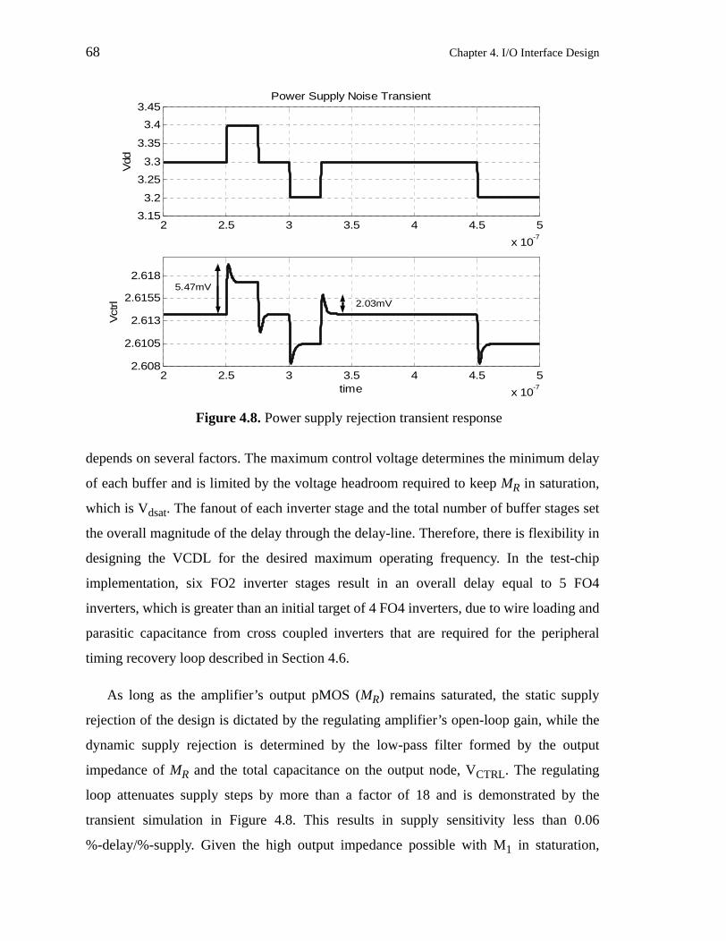
68 Chapter 4. I/O Interface Design
depends on several factors. The maximum control voltage determines the minimum delay
of each buffer and is limited by the voltage headroom required to keep MR in saturation,
which is Vdsat. The fanout of each inverter stage and the total number of buffer stages set
the overall magnitude of the delay through the delay-line. Therefore, there is flexibility in
designing the VCDL for the desired maximum operating frequency. In the test-chip
implementation, six FO2 inverter stages result in an overall delay equal to 5 FO4
inverters, which is greater than an initial target of 4 FO4 inverters, due to wire loading and
parasitic capacitance from cross coupled inverters that are required for the peripheral
timing recovery loop described in Section 4.6.
As long as the amplifier’s output pMOS (MR) remains saturated, the static supply
rejection of the design is dictated by the regulating amplifier’s open-loop gain, while the
dynamic supply rejection is determined by the low-pass filter formed by the output
impedance of MR and the total capacitance on the output node, VCTRL. The regulating
loop attenuates supply steps by more than a factor of 18 and is demonstrated by the
transient simulation in Figure 4.8. This results in supply sensitivity less than 0.06
%-delay/%-supply. Given the high output impedance possible with M1 in staturation,
2 2.5 3 3.5 4 4.5 5
x 10-7
3.15
3.2
3.25
3.3
3.35
3.4
3.45Power Supply Noise Transient
Vdd
2 2.5 3 3.5 4 4.5 5
x 10-7
2.608
2.6105
2.613
2.6155
2.618
Vct
rl
time
5.47mV
2.03mV
Figure 4.8. Power supply rejection transient response

Chapter 4. I/O Interface Design 69
there is a trade-off between the size of the capacitor at the output and its effect on the
bandwidth. As mentioned earlier, a sufficiently high bandwidth is needed to keep it from
compromising the stability of the enclosing loop. Bandwidth ratio between the two loops
on the order of 10x is desirable. Given the good noise rejecting properties of this
regulating amplifier, a low-jitter delay line consisting of supply-controlled inverters can be
obtained. Its operation is in some ways similar to replica-biased differential delay
elements [31]. While replica biasing in the differential buffers dynamically adjusts its
current to compensate for power supply fluctuations, the regulating amplifier rejects
power supply noise to the control voltage itself. Filtering the control voltage through the
regulating amplifier also provides good dynamic noise immunity.1
To maintain high saturation margins in the amplifier while delivering power to the
delay line, the amplifier current is set to be larger than the current consumed by the VCDL
delay elements. There is a factor of three to four between the delivered current through the
second stage and current delivered. Small offsets that may result due to imbalance in the
amplifier do not affect operation since its compensated by negative feedback in the
enclosing delay-locked loop.
Frequency-Tracking Differential Charge-Pump
One of the advantages of using delay lines with supply-controlled inverters is that their
delay range is very broad. However, this broad range comes at the expense of a
non-linearly varying delay-line gain over the operating frequency range. Transfer function
of a conventional charge-pump DLL modeled with a single dominant pole:
, (4-3)
where ωp represents the dominant pole frequency (also equivalent to the loop bandwidth).
Ideally, we want ωp to track with FREF so that the loop bandwidth is always 10 - 20x lower
than the operating frequency. Then, the fixed delay around the loop only causes a small
1 Unfortunately, regulating the supply voltage does not make the cells immune to substrate noise, butthe larger Vgs values make these elements less sensitive to substrate noise.
H s( ) 11 s ωP⁄+----------------------=

70 Chapter 4. I/O Interface Design
phase excess phase shift. ωp is:
, (4-4)
where CCP is the charge-pump capacitance, KDL is the delay-line gain, and FREF is the
input frequency. ωp would track FREF if KDL, ICP, and CCP were constant and sized to
guarantee a stable configuration.
Unfortunately, for a delay line consisting of supply-controlled inverters, its delay
versus VCTRL is governed by the following equation:
(4-5)
where β represents device transconductance, N represents the number of inverters in the
delay line, and α corresponds to the exponent in the alpha power model approximation of
the saturation current of an inverter, which accounts for velocity saturation effects. A
numerical fit of the simulated delays of an inverter in a HP0.35µm CMOS process with
the above equation and α=1.3 is presented in Figure 4.9 and shows good agreement. KDL
ωP
ICP KDL FREF⋅ ⋅CCP
----------------------------------------=
TDELAY
N CLD VCTRL⋅ ⋅
β VCTRL VTHÐ( )α----------------------------------------------=
Figure 4.9. Normalized delay-line delay vs. supply voltage
0
0.2
0.4
0.6
0.8
1
1 1.5 2 2.5 3 3.5
Nor
mal
ized
Del
ay-L
ine
Del
ay
Supply Voltage (V)
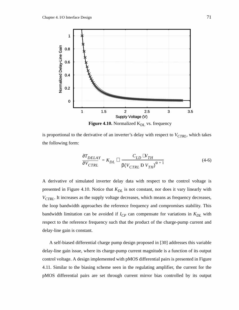
Chapter 4. I/O Interface Design 71
is proportional to the derivative of an inverter’s delay with respect to VCTRL, which takes
the following form:
(4-6)
A derivative of simulated inverter delay data with respect to the control voltage is
presented in Figure 4.10. Notice that KDL is not constant, nor does it vary linearly with
VCTRL. It increases as the supply voltage decreases, which means as frequency decreases,
the loop bandwidth approaches the reference frequency and compromises stability. This
bandwidth limitation can be avoided if ICP can compensate for variations in KDL with
respect to the reference frequency such that the product of the charge-pump current and
delay-line gain is constant.
A self-biased differential charge pump design proposed in [30] addresses this variable
delay-line gain issue, where its charge-pump current magnitude is a function of its output
control voltage. A design implemented with pMOS differential pairs is presented in Figure
4.11. Similar to the biasing scheme seen in the regulating amplifier, the current for the
pMOS differential pairs are set through current mirror bias controlled by its output
VCTRL∂∂TDELAY KDL=
CLD VTH⋅
β VCTRL VTHÐ( )α 1+------------------------------------------------------∝
Figure 4.10. Normalized KDL vs. frequency
0
0.2
0.4
0.6
0.8
1
1 1.5 2 2.5 3 3.5
Nor
mal
ized
Del
ay-L
ine
Gai
n
Supply Voltage (V)
0
0.2
0.4
0.6
0.8
1
1 1.5 2 2.5 3 3.5
Nor
mal
ized
Del
ay-L
ine
Gai
n
Supply Voltage (V)
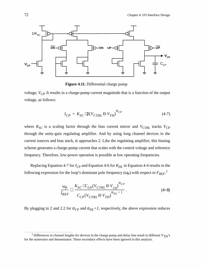
72 Chapter 4. I/O Interface Design
voltage, VCP. It results in a charge-pump current magnitude that is a function of the output
voltage, as follows:
(4-7)
where KSC is a scaling factor through the bias current mirror and VCTRL tracks VCP
through the unity-gain regulating amplifier. And by using long channel devices in the
current sources and bias stack, α approaches 2. Like the regulating amplifier, this biasing
scheme generates a charge-pump current that scales with the control voltage and reference
frequency. Therefore, low-power operation is possible at low operating frequencies.
Replacing Equation 4-7 for ICP and Equation 4-6 for KDL in Equation 4-4 results in the
following expression for the loop’s dominant pole frequency (ωP) with respect to FREF.1
. (4−8)
By plugging in 2 and 2.2 for αCP and αDL+1, respectively, the above expression reduces
1 Differences in channel lengths for devices in the charge pump and delay line result in different VTH’sfor the numerator and denominator. These secondary effects have been ignored in this analysis.
UPDNDN
VCP
VCP
CCP
1/KSC
UP
Figure 4.11. Differential charge pump
ICP KSC β VCTRL VTHÐ( )αCP⋅=
ωP
fREF-----------
KSC CLD VCTRL VTH
Ð( )αCP⋅
CCP VCTRL VTHÐ( )αDL 1+
--------------------------------------------------------------------------∝

Chapter 4. I/O Interface Design 73
to the following expression:
(4−9)
There is only a weak dependence on VCTRL and results in a relatively constant ratio
between the loop’s bandwidth and operating frequency. This ratio is only a function of a
well controlled scaling factor KSC and the ratio of two capacitors. A large nMOS device
implements the loop filter capacitor, CLF. Therefore, CLF and CLD, consisting primarily of
gate capacitance, track well over process, temperature, and voltage, and result in
predictable loop characteristics.
Although this self-biased charge-pump design offers good bandwidth characteristics
across a wide range of frequencies, it limits the frequency lock range for the DLL. The
charge-pump output’s upper range is constrained by the voltage required to keep the
current source and differential pair in saturation (Vdd - 2Vdsat). The lower range is set by
the diode connected nMOS loads (VTHn). A design that implements a pMOS differential
pair with wide current source and differential pair devices was chosen since it enables a
higher upper range compared to a design that utilizes nMOS differential pairs with pMOS
loads. Furthermore, pMOS inputs can directly interface to lower common-mode voltage
swings from the phase detector. Unfortunately, the phase detector was initially designed
with an nMOS differential in mind and therefore utilize low-to-high swing converters and
do not take advantage of this property. Detailed descriptions of both the phase detector and
low-to-high swing converters follow next.
Phase Detector
The charge pump is driven by a phase detector (PD) that compares the 0 and 180 degree
clock edge outputs of the delay line and generates UP and DN whose relative pulse widths
represent the mismatch between the two clock edges. A wider UP pulse signifies that the
180 degree clock edge lags behind the 0 degree clock edge, telling the charge pump to
raise the control voltage and reduce delay through the delay line. A wider DN pulse
signifies that the 180 degree clock edge leads the 0 degree clock. When the two edges are
ωP
fREF-----------
KSC CLD⋅
CCP VCTRL VTHÐ( )0.2---------------------------------------------------------∝
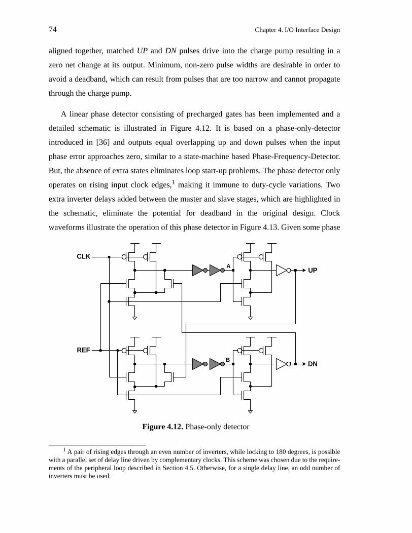
74 Chapter 4. I/O Interface Design
aligned together, matched UP and DN pulses drive into the charge pump resulting in a
zero net change at its output. Minimum, non-zero pulse widths are desirable in order to
avoid a deadband, which can result from pulses that are too narrow and cannot propagate
through the charge pump.
A linear phase detector consisting of precharged gates has been implemented and a
detailed schematic is illustrated in Figure 4.12. It is based on a phase-only-detector
introduced in [36] and outputs equal overlapping up and down pulses when the input
phase error approaches zero, similar to a state-machine based Phase-Frequency-Detector.
But, the absence of extra states eliminates loop start-up problems. The phase detector only
operates on rising input clock edges,1 making it immune to duty-cycle variations. Two
extra inverter delays added between the master and slave stages, which are highlighted in
the schematic, eliminate the potential for deadband in the original design. Clock
waveforms illustrate the operation of this phase detector in Figure 4.13. Given some phase
1 A pair of rising edges through an even number of inverters, while locking to 180 degrees, is possiblewith a parallel set of delay line driven by complementary clocks. This scheme was chosen due to the require-ments of the peripheral loop described in Section 4.5. Otherwise, for a single delay line, an odd number ofinverters must be used.
A
CLK
REF
UP
DNB
Figure 4.12. Phase-only detector

Chapter 4. I/O Interface Design 75
offset, where the 180 degree clock out of the delay-line is late, the early clock edge
triggers UP to transition high. The rising edge of the late clock triggers DN to go high and
both internal nodes A and B to fall, which in turn precharges the second stage and both
outputs reset to zero. The difference between the generated pulse widths is linear with the
phase difference between the two inputs. The two additional inverters delay the internal
nodes (A and B) from prematurely resetting the output and the phase detector generates a
minimum pulse even when the two input phases are aligned. This eliminates the deadband
that can occur due to extremely narrow pulses that cannot propagate through to the charge
pump when the phases are nearly matched. The subsequent falling edge of the clocks
precharge the first stage, but do not affect the output pulses. Lastly, since a
phase-only-detector receives no information about frequency, a sub-harmonic lock
condition can potentially occur, where the delay-line locks to N+1/2 periods. The DLL
avoids this condition by resetting the delay line to have minimum delay at system start-up.
A simple low-to-high swing converter, presented in Figure 4.14, takes the low voltage
swings from the delay line and converts them into full-swing digital signals that drive the
phase detector, which operates off of the high supply voltage. The converter takes a
differential input voltage and the second stage generates a single-ended full-swing signal
through current mirrors that actively drive the output both high and low. The inputs to the
differential pair are driven with low fanout inverters to reduce the effect of device
REF
CLK
A
UP
B
DN
Figure 4.13. Phase detector transient waveforms

76 Chapter 4. I/O Interface Design
mismatches and result in low static phase error. This converter can operate with very low
input voltages, less than 1-V, since its operation relies on current differences and high
gains are achievable with high-gm input devices.
Although good performance is possible with this low-to-high swing converter, it is
actually not needed. The phase detector, running at the full clock rate, consists of dynamic
gates which can operate off of the regulated supply where its delay tracks with the
delay-line inverters. Furthermore, the differential charge pump can operate with
low-swing inputs since a pMOS differential pair is a good fit for the low common mode of
signals generated by the lower regulated supply voltage. However, since this observation
was made after the chip was fabricated, the DLL in the test-chip prototype consumes more
power than is ideal.
4.2.1 Summary
In this section, a core DLL that uses supply-controlled inverters, which models the critical
path, as delay elements locks to an input reference clock and determines the “right”
voltage of operation for the rest of the I/O subsystem. By implementing this loop in the
same die as the rest of the I/O subsystem, the delays of all other digital gates that operate
off of the local supply voltage set by the DLL tracks with the inverters in the delay line.
Hence, these delays are a fixed percentage of the reference clock period across process
IN
IN
OUT
Figure 4.14. Low-to-high swing converter

Chapter 4. I/O Interface Design 77
and environmental variations. This property offers an interesting potential for building the
I/O transceiver blocks with several desirable characteristics.
4.3 Transmitter Design
The next block in the link interface is the transmitter that converts binary data into
electrical signals that propagate through an impedance-controlled channel (or transmission
line) to a receiver at the opposite end. This must be done with accurate signal levels and
timing for high-speed communication links.
Given two chips that communicate with each other with dynamically regulated
voltages, their voltages can differ greatly due to their individual process and temperature
conditions. Many conventional high-speed interfaces use current-mode transmitters with
an ECL type interface, where transmitted and received signals swing relative to the upper
rail. However, this configuration poses a potential problem when operating off of a
regulated supply. Besides the transmit and receive sides each having potentially different
supply voltages, they are each within larger chips, which can also contain other supply
voltage levels. For NWELL technologies, the common reference for all the chips must be
ground. Otherwise, if all the different voltages share a common high rail, resulting
threshold voltage shifts due to back bias effects significantly reduces the performance for
lower voltage blocks. Therefore, ground is chosen to be the common voltage reference for
communication. An advantage of having ground as the common reference is that it
enables compatibility with different CMOS technologies for the transmitter and receiver
chips [2]. A pMOS current source based high-impedance driver that operates off of the
same regulated voltage as the rest of the system was implemented in the test-chip
prototype and properties associated with its operation in an adaptively regulated supply
voltage environment are described in this section.
Section 4.3.1 begins with a description of the transmitter design which has options for
both single-ended and differential modes of operation. As discussed in Section 4.1,
controlling the slew rate of transmitted signals is desirable for reducing noise and improve
link performance. So, Section 4.3.2 then describes how a dynamically scaled supply

78 Chapter 4. I/O Interface Design
voltage environment offers automatic slew-rate control without the need for additional
hardware.
4.3.1 High-Impedance Drivers
High-speed links commonly rely on high-impedance drivers to efficiently convert binary
data bits into electrical signals that propagate through the channel [19]. These signals are
generated via a current source that turns on and off depending on the polarity of the
transmitted data. Figure 4.15 presents a schematic of a driver that utilizes a current source
that actively pulls up the output to generate signals in the channel that swing relative to
ground. The voltage swing seen at the receiver depends on the magnitude of the current
and the termination scheme used. There are multiple options for termination. Placing a
single termination resistor on the transmitter side yields an impedance-matched driver and
is used in the test-chip prototype. Current pulled through the current source launches a
voltage waveform through the channel, with a swing magnitude set by the current
magnitude times the parallel combination of the termination resistor and channel
impedance.
(4-10)
The receiver input capacitance presents a high-impedance load so that the waveform
reflects off of the open termination of the receiver, doubling the swing magnitude at the
Figure 4.15. Ideal high-impedance driver
Rtermination
Zchannel
Isrc
swing Isrc Rtermination Zchannel||( )⋅=

Chapter 4. I/O Interface Design 79
receiver, and traverses back to the source. Given a termination resistor at the source
(transmitter) that matches the characteristic impedance of the channel, the energy from the
reflected wave is completely absorbed in the resistor. One can see that this scheme
requires good matching between the termination and channel impedance. Otherwise,
mismatches result in energy sloshing back and forth between the transmitter and receiver
and increase the effective noise on the signal. Therefore, in addition to a fixed termination
resistance, it is important for the current source to remain in saturation throughout its
output swing so that potential variations in its output impedance, which lies in parallel
with the termination resistor, do not significantly affect the termination resistance seen by
the reflected wave.
In the test-chip prototype, the current source for the high-impedance driver utilizes a
pMOS current source with a termination resistor to ground, implemented with nMOS
devices, and is shown in Figure 4.16. A 2:1 multiplexor enabled by a pair of
complementary clocks generates data bits on every clock phase and a set of predriver
inverters drive the input of the pMOS current source. As long as the output swings with a
magnitude less than Vdd-Vdsat, the pMOS current source remains in saturation throughout
its swing. Besides the termination devices, all components of the transmitter block operate
off of the regulated supply voltage. Operation across a wide operating frequency and
subsequently wide regulated voltage range is achievable, since Vdsat reduces with the
sel[5:0]
ΦΦ
Figure 4.16. Single-ended transmitter
80 Chapter 4. I/O Interface Design
voltage swing magnitude at the input of the current source. Along with the
high-impedance of the current source, parallel on-chip termination, implemented with
nMOS devices operating in the linear region, provides a nominally fixed resistance. To
ensure that the nMOS devices operate in the linear region throughout the output swing of
the transmitter, the select signals are supplied off of the high supply voltage (3.3V).
Potential process and environmental variations require resistor tuning, and is made
possible with a parallel set of binary weighted devices that can be turned on and off
through a configuration register.1 This digital tuning capability comes at expense of higher
capacitive loading at the transmitter, caused by the parasitic drain and overlap capacitance
of the off transistors. Fortunately, the added capacitance was small enough not to affect
link speed.
One major source of noise in most single-ended transmitters results from the switching
current in the supply lines. Since the current is sent out the output line, the return current
must flow in through the power supply pins. Parasitic inductance and resistance in the this
return path results in noise being generated on the chip supplies. With parallel links, the
aggregate current magnitude can be large and result in large voltage noise magnitudes. A
differential output eliminates this noise since the supply current for each output pair is
constant. Therefore, in order to investigate the difference between single-ended and
differential signalling, the test chip also implements an option to utilize a pair of
transmitters that transmit differential data, as shown in Figure 4.17. A drawback of
differential signaling stems from the need for an additional pin per I/O and potentially
doubling the power consumption since there are double the number of transmitters that
switch. However, reduction in transmitter noise possible through differential signalling
may enable lower signaling levels to reduce the overall power consumed, relative to
single-ended signalling. Differential signalling also eliminates an additional source of
noise in single-ended transmitters. In order to decipher the polarity of a single-ended
signal, a receiver needs a reference voltage that lies in the middle of the signal swing for
1 Production parts typically implement a slow feedback loop to tune this resistance with respect to pro-cess and environmental variations. In this test-chip prototype, tuning is performed manually through config-uration registers that are set externally.

Chapter 4. I/O Interface Design 81
comparison. This is easily achieved with a transmitter that constantly sources half the
current required for a full signal swing and transmitting it in parallel with the data. In order
to save pin resources, a single reference is typically shared by multiple receivers.
However, this makes the reference susceptible to noise coupling in from several
transceivers which affects all the parallel links. Experimental results are described in
Section 4.6.
4.3.2 Impedance, Current and Slew-Rate Control
In order to achieve robust, high-speed operation, the transmitter must accurately control
its output swing magnitude and slew rate. This task is challenging since both parameters
can depend on process, temperature, and voltage. Although process variation is fixed for a
single chip, on-die temperature can vary with time and therefore requires an active
mechanism to compensate for its changes. As shown in Figure 4.18, transmitter designs
commonly utilize a set of binary weighted current source legs driven by NAND gates that
are driven by a common data signal and individually driven by control bits that set the
number of current sources enabled. A servo-A/D based control loop is often used to set the
appropriate sizing in response to process and temperature conditions [26]. An adaptively
regulated supply voltage has the advantage of offering this process and temperature
tracking automatically. Since the regulated supply voltage is set based on the speed of a
Data
Data
Figure 4.17. Differential signaling
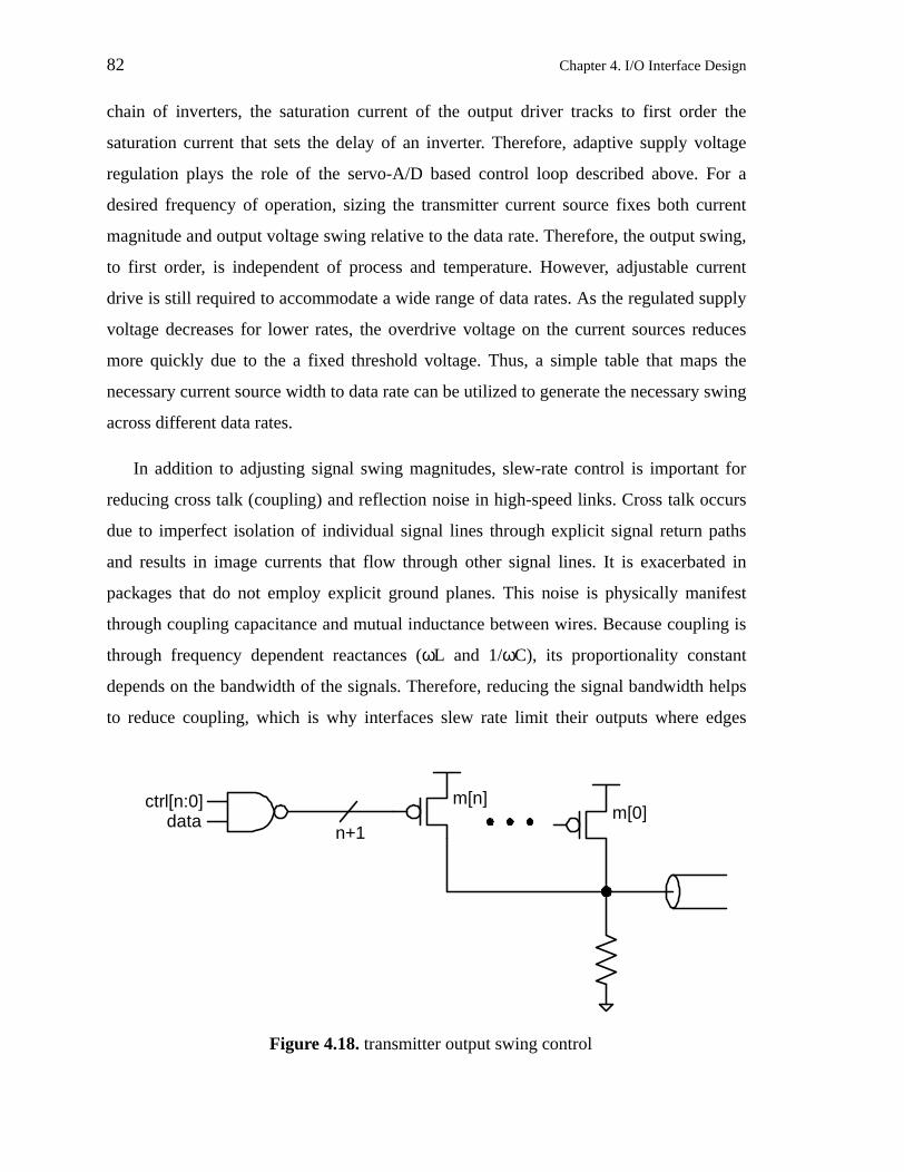
82 Chapter 4. I/O Interface Design
chain of inverters, the saturation current of the output driver tracks to first order the
saturation current that sets the delay of an inverter. Therefore, adaptive supply voltage
regulation plays the role of the servo-A/D based control loop described above. For a
desired frequency of operation, sizing the transmitter current source fixes both current
magnitude and output voltage swing relative to the data rate. Therefore, the output swing,
to first order, is independent of process and temperature. However, adjustable current
drive is still required to accommodate a wide range of data rates. As the regulated supply
voltage decreases for lower rates, the overdrive voltage on the current sources reduces
more quickly due to the a fixed threshold voltage. Thus, a simple table that maps the
necessary current source width to data rate can be utilized to generate the necessary swing
across different data rates.
In addition to adjusting signal swing magnitudes, slew-rate control is important for
reducing cross talk (coupling) and reflection noise in high-speed links. Cross talk occurs
due to imperfect isolation of individual signal lines through explicit signal return paths
and results in image currents that flow through other signal lines. It is exacerbated in
packages that do not employ explicit ground planes. This noise is physically manifest
through coupling capacitance and mutual inductance between wires. Because coupling is
through frequency dependent reactances (ωL and 1/ωC), its proportionality constant
depends on the bandwidth of the signals. Therefore, reducing the signal bandwidth helps
to reduce coupling, which is why interfaces slew rate limit their outputs where edges
ctrl[n:0] m[n]m[0]data
n+1
Figure 4.18. transmitter output swing control

Chapter 4. I/O Interface Design 83
consume a quarter to a third of the bit time.
In conventional designs, limiting the slew rate can be difficult, and several approaches
have been published [19],[26],[9]. However, a dynamically regulated supply voltage
environment again provides the process and environment monitoring required to
automatically control the output slew rate without any additional hardware. The core DLL
locks the delay of inverters in the delay-line to half a clock period. This means that the
delay of each inverter is a fixed percentage of the clock period. This also hold true for the
edge rates of the internal signals in the delay-line and for other digital circuits operating
off the same regulated voltage. Therefore, setting the transition times of the predriver to a
fixed percentage of the bit time through sizing ensures this percentage to remain fixed
across a wide range of process, temperature, and clock frequencies. A potential concern of
using this approach comes from the short-circuit current that may arise due to slow edge
rates at the output of the predrivers. Given a clock frequency that corresponds to 8 FO4
inverter delays, transition times that consume a third of the bit time nominally correspond
to the output transition time of a FO4 inverter. This fanout is typically found in general
digital CMOS circuits and therefore short circuit currents are not especially significant.
However, operating both the output driver and predriver off the same regulated supply
voltage with controlled slew rates creates a different problem. Due to the finite threshold
voltage of the current source devices, current does not flow until the gate is below a
threshold voltage. This means that a fifty percent duty-cycle input to the output driver
generates a narrower pulse at the output. Duty-cycle distortion directly affects timing
margins and is critical to link performance. To address this distortion, the predrivers
pre-shape its output to generate the desired 50-% duty-cycle pulse width at the output of
the high-impedance driver. The shaping is achieved by properly sizing the PN ratios of the
two inverting buffers shown in Figure 4.19. A digital control word selectively enables
parallel legs to change its effective pull-up and pull-down drive strengths. A pair of these
buffers are used to make it immune to p-to-n skews. Unfortunately, with this solution, the
PN ratio configuration does not track with voltage and only works for limited voltage
ranges. A simple control loop can be used to adjust these buffers to accommodate a wider
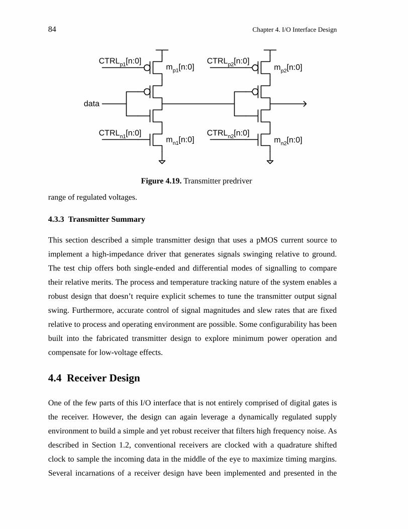
84 Chapter 4. I/O Interface Design
range of regulated voltages.
4.3.3 Transmitter Summary
This section described a simple transmitter design that uses a pMOS current source to
implement a high-impedance driver that generates signals swinging relative to ground.
The test chip offers both single-ended and differential modes of signalling to compare
their relative merits. The process and temperature tracking nature of the system enables a
robust design that doesn’t require explicit schemes to tune the transmitter output signal
swing. Furthermore, accurate control of signal magnitudes and slew rates that are fixed
relative to process and operating environment are possible. Some configurability has been
built into the fabricated transmitter design to explore minimum power operation and
compensate for low-voltage effects.
4.4 Receiver Design
One of the few parts of this I/O interface that is not entirely comprised of digital gates is
the receiver. However, the design can again leverage a dynamically regulated supply
environment to build a simple and yet robust receiver that filters high frequency noise. As
described in Section 1.2, conventional receivers are clocked with a quadrature shifted
clock to sample the incoming data in the middle of the eye to maximize timing margins.
Several incarnations of a receiver design have been implemented and presented in the
mp1[n:0]
mn1[n:0]
mp2[n:0]
mn2[n:0]
CTRLp1[n:0]
CTRLn1[n:0]
CTRLp2[n:0]
CTRLn2[n:0]
data
Figure 4.19. Transmitter predriver

Chapter 4. I/O Interface Design 85
literature [11],[51],[12] to maximize performance. Sidiropoulos shows that proper
sampling of the data alone may not guarantee the receiver recovers the correct data value
due to noise that may couple in at the moment of sampling [44]. Therefore, two-stage
receiver designs are commonly used, where the first stage acts to condition the input noise
in the incoming signal and the second stage amplifies the signal to full-swing digital data.
An integrating receiver fully described and analyzed in [40] offers good filtering
capability since its bandwidth is set by the integration time, which is equivalent to the bit
time. However, it requires accurate phase alignment between the clock and data.
The test-chip receiver also relies on a two stage receiver, comprised of a bandwidth
limiting amplifier followed by a regenerative latch, illustrated in Figure 4.20. It offers
flexible operation by accommodating both single-ended and differential transmitted
signals with configurable nMOS switches at the input to the preamplifier. In order to
minimize potential filtering effects due to the pass gates, the gates are switched using the
high supply voltage. Supply noise that couples in from this high supply voltage through
the switches is common mode to the receiver and therefore has a negligible effect on
receiver performance. A reference voltage (VREF) that is set to half the swing magnitude
and sent along with the transmitted signals is shared by all the receivers for receiving
single-ended signals. 2-1 demultiplexing for the double data-rate signal require two
samplinglatch
SRFFpreamp
Φ0 Φ1
DIN
outMVREFsampling
latchSRFFpreamp
Φ0 Φ1
outP
DIN
Figure 4.20. Receiver block diagram

86 Chapter 4. I/O Interface Design
parallel receiver paths that operate on complementary clock phases, where one
preamplifer evaluates during half a clock cycle while the other resets. A pair of
regenerative latches sample the output of the preamplifier on the falling edge of a delayed
clock Φ1 and Φ1. Precise positioning of this clock is discussed in Section 4.4.2.
Subsequent set-reset flip flops (SRFF) hold the outputs for an entire clock cycle and
ultimately drive into retiming circuitry in order to synchronize the data to the system clock
of the digital system that consumes the data. In the test chip, the received data is driven off
chip and to internal decode logic to verify proper operation.
4.4.1 Bandwidth-Tracking Preamplifier
The first stage of the receiver is a preamplifier consisting of a pMOS differential pair
with nMOS linear loads, as shown in Figure 4.21. pMOS inputs are chosen due to the low
common mode of the transmitted signals. The preamplifier resets while Φ0 is high and its
outputs are equalized through a shorting nMOS device. While Φ0 is low, the stage
amplifies the signal for a full bit period. The preamplifier operates off of the regulated
supply and the current source to the pMOS differential pair is biased through a replica
self-biasing scheme [23]. A half-replica of the differential preamplifier is used in the bias
generator and its output drives the positive input of an amplifier, while the negative input
is biased to around VTHn. The output of the amplifier drives the current source of the
Bias Gen
Preamplifier
Φ0
IN IN
OUT OUT
weak
large
Figure 4.21. Preamplifier schematic

Chapter 4. I/O Interface Design 87
half-replica and preamplifiers, and with feedback, the preamplifier’s output swing
magnitude is clamped to a swing of VTHn.
The bandwidth of the preamplifier is set by the RC product between the capacitive
loading on the output of the preamplifier and its output resistance. This resistance is
dominated by the nMOS load device throughout its swing. Since the supply to the gates of
these nMOS loads is again the regulated voltage, their output resistance is effectively also
regulated. To first order, the small signal output resistance of a non-minimum channel
MOS device is inversely proportional to Idsat, and tracks the saturation current that sets the
delay of inverters in the delay-line of the core DLL. So feedback in the DLL that sets the
regulated voltage magnitude also enables the bandwidth of the input receiver to track the
bit rate of the link. This is advantageous because the bandwidth can be set to only allow in
frequency components up to the bit rate and filter out unwanted high-frequency noise.
This tracking filter property of the receiver’s preamplifier can be verified across
process corners by observing the output swing of the preamplifier versus a phase offset
swept between the input data and clock (Φ0) waveforms. Figure 4.22 plots the differential
output swing of the preamplifier while sweeping 200mV single-ended input data
-0.5 0 0.5 1 1.5 2 2.5
x 10-9
-0.15
-0.1
-0.05
0
0.05
0.1
0.15
Preamplifier differential output vs. process corner
clk-to-data phase offset (s)
diffe
rent
ialo
utpu
t(V
)
Figure 4.22. Preamplifier differential output versus process corner

88 Chapter 4. I/O Interface Design
transitions relative to a 400MHz clock. Since the supply voltage of the preamplifier
dynamically adjusts to the process corner, the time constants of the waveforms are similar
for five process corners (TT, FF, SS, FS, and SF). Hence, it shows that the preamplifier’s
filtering property is independent of the operating conditions. Figure 4.23 shows that the
RC filter also tracks relative to frequency, and plots normalized differential output voltage
waveforms versus normalized phase offsets between clock and data at seven different bit
rates ranging from 150 to 450 MHz.
Low-Voltage Limitations
One of the limitations that this preamplifier imposes on the receiver design stems from its
minimum voltage headroom requirements. The current source and differential pair must
be in saturation and requires at least 2Vdsat’s across the pMOS devices and a VTP from the
gate to source of the differential pair. Therefore, the total voltage headroom required is:
(4-11)
which corresponds to 1.3-V in a HP0.35µm process. Digital CMOS logic gates that
dominate the rest of the I/O subsystem do not suffer from this limitation and can operate
-0.2 0 0.2 0.4 0.6 0.8 1
-1
-0.8
-0.6
-0.4
-0.2
0
0.2
0.4
0.6
0.8
1
Normalized preamplifier differential output vs. bit rate(150 - 450 MHz)
Normalized cycle time
Nor
mal
ized
diffe
rent
ialo
utpu
t
Figure 4.23. Preamplifier differential output versus bit rate
VHEADROOM VTP 2Vdsat+=

Chapter 4. I/O Interface Design 89
well below this minimum headroom voltage level at the expense of slower operation.
Since this preamplifier, along with the rest of the digital logic, operates off of the lower
regulated voltage, the minimum operating range of the I/O interface is set by this voltage
headroom limitation.
4.4.2 Regenerative Latch and Timing
The requisite high-gain second stage consists of a clocked regenerative latch that converts
the limited swing output of the preamplifier to a full-swing digital signal and is shown in
Figure 4.24. Its structure is that of a commonly used high-speed latch found in the
strongARM processor [10] and its operation is straight forward. While Φ1 clock is high,
the latch resets by disabling the PMOS evaluation transistor and equalizing the two sides
of the differential pair to low. On the falling edge of Φ1, the latch begins evaluation and
samples the differential voltage across its inputs. Regeneration through the cross coupled
nMOS and pMOS devices quickly resolve full swing signals at the outputs. This type of
regenerative latch offers the best speed, power, and area trade-off, and given its digital
in
Φ1
out
in
out
SRFF
Figure 4.24. Regenerative latch and SRFF

90 Chapter 4. I/O Interface Design
nature, it can operate off of the regulated voltage and its delay tracks relative to the delay
of an inverter. The regenerative latch is followed by a standard SRFF, implemented with
cross-coupled NAND gates, to hold the data received on each phase of the clock for an
entire clock period.
The timing for the two clock signals required by the receiver are presented in Figure
4.25. Φ0 must be aligned with the incoming data signal to evaluate during a single clock
phase. A pair of receivers operating on complementary clock phases are therefore required
to receive data on both phases of the clock. Once the preamplifier begins evaluation, it
amplifies the incoming signal and holds the value until the subsequent regenerative latch
samples the preamplifier output. Ideally, the regenerative latch ought to sample after the
preamplifier has amplified the incoming signal over nearly the entire bit time, which
makes this receiver behave like an integrating receiver. Although 135 degrees or more
offset between Φ0 and Φ1 offers better receiver margins, the test chip offsets the sampling
edge by only 90 degrees. This is due to the configuration of the phase detecting receiver in
the peripheral loop used for aligning the internal clocks to the incoming I/O clock which is
discussed thoroughly in Section 4.5.
4.4.3 Receiver Summary
This section described the design of the receiver that consists of two stages: one to filter
out high frequency noise, and the other to convert the incoming low swing signal into
DIN
Φ0
Φ1
D0
outP
outM
D1
D1 D2 D3
D3
D0 D2
Figure 4.25. Receiver timing
Chapter 4. I/O Interface Design 91
full-swing digital signals. The preamplifier operates off of the regulated not only so that its
power consumption tracks with the bit rate, but it relies on the regulated voltage to set its
input bandwidth and have it also track with the bit rate. The regenerative latch is a digital
circuit block that translates the low-swing output of the preamplifier into full-swing digital
signals and also operates off of the regulated supply. One drawback of this approach to
receiver design stems from the analog nature of the preamplifier which requires a
minimum overhead voltage and limits the lower frequency range of operation. Therefore,
other techniques that can reduce or circumvent this minimum voltage headroom limitation
is required for future technologies where VTH does not scale down as quickly as circuit
delays and supply voltage.
While mimicking the filtering properties of an integrating amplifier, this receiver
design offers a simpler solution that does not require the sample and hold stage necessary
in the integrating receiver design. Although the sample and hold stage can easily be
implemented with a simple pass gate network, its operation does not scale well with lower
supply voltages due to the body-effected VTN of the pass transistors. Therefore, extra care
must be taken to design an integrating receiver design that operates off of a lower
regulated supply voltage.
Operation of the receiver and performance of the link heavily rely on the alignment of
the clocks that trigger the preamplifier and regenerative latch, to the incoming data signal.
This is achieved with a digital peripheral loop that locks the internal clock signals relative
to the incoming parallel I/O clock and is the topic of the next section.
4.5 Timing Recovery
Timing recovery is a crucial component of high-speed interfaces and can take several
different forms. In the case of a source synchronous parallel interface design that transmits
a dedicated clock signal along with the data, timing recovery can be achieved with a single
delay-locked loop. This section first describes a digital implementation of the peripheral
loop of a dual-loop DLL design [43] that aligns the internal clock signal with the incoming
I/O clock. A fully digital peripheral loop is possible by again leveraging the delay

92 Chapter 4. I/O Interface Design
controlled nature of digital gates with an adaptively regulated supply and replace precision
analog circuit elements that would otherwise be used. Even the analog-like function of
interpolation that is required by the loop can be performed in a completely digital fashion.
Subsection 4.5.2 then describes a duty-cycle adjusting circuit that operates on full-swing
CMOS signals. Lastly, issues associated with clock distribution for this I/O interface
design are discussed.
4.5.1 Dual-loop architecture
The timing recovery block relies on a dual-loop DLL architecture that uses the core
DLL, described in Section 4.1, to generate 12 evenly spaced clock edges that span 360o
and drive into a digital peripheral loop that generates the desired clocks. The digital
peripheral loop selects an adjacent pair of edges, and interpolates between them to finely
align a clock edge relative to the input I/O clock. This dual-loop configuration enables
unlimited capture range and allows a wide frequency range of operation. An architectural
block diagram of the dual-loop architecture is presented in Figure 4.26. In the
mux-interpolator data paths, a pair of multiplexors each select one of a pair of adjacent
clock edges out of twelve edges that are each spaced an inverter delay apart. These twelve
evenly spaced edges can be generated by implementing a parallel set of delay lines in the
core DLL, consisting of six inverters each, and driven with complementary reference
clock signals. The weak feedback inverters keep the clocks propagating through the
parallel paths aligned in phase. The two adjacent clocks then feed into an interpolating
block that generates a clock that can be finely placed relative to the two input clocks and is
controlled by changing the relative contribution of the two clock edges to the output.
Interpolation allows the resolution of clock placement to be much better finer than a single
inverter delay. The interpolator output then drives through a duty-cycle adjuster and clock
distribution buffers before clocking a receiver that acts as a phase detector for the
peripheral loop. The phase detector output generates up and down pulses to a finite-state
machine (FSM) which then closes the loop by controlling mux and interpolator settings.
An additional mux-interpolator datapath generates the delayed clock Φ1, which is offset
from Φ0. Adding a digital offset to the control bits in the FSM that set the interpolated

Chapter 4. I/O Interface Design 93
edge for Φ0 enables a simple mechanism for generating the control bits that drive the
second Φ1 mux-interpolator datapath to create this static offset.
The original implementation of this dual-loop architecture uses analog differential
delay buffers in the core delay line and interpolator with a sophisticated replica biasing
scheme [43]. With an adaptively regulated supply, simple digital gates can replace the
precision analog blocks in the peripheral loop since the performance of these gates track
with link frequency. The multiplexors that select adjacent clock edges are implemented
with transmission gates whose delays track well with the delay of an inverter across
process, voltage and temperature. Therefore, the delay through these gates are always a
fixed percentage of the clock period when operating off of the adaptively regulated supply.
The control signals for the multiplexors and interpolator come from a digital finite
state machine (FSM) that consists of a simple binary up/down counter and decoder. Each
Core DLL Delay-Line
Φ0 Mux-Interpolator Datapath
FSM
Φ0
RX/PDI/O ClkUP/DN
0
30
60
90
120
150180
210
240
270
300
330
Φ1 Mux-Interpolator Datapath
DCA &Buffers
Φ1
ctrl
Figure 4.26. Digital peripheral loop

94 Chapter 4. I/O Interface Design
counter value corresponds to one of 192 possible edge positions within a clock cycle. A
data receiver connected to the incoming parallel I/O clock acts as a bang-bang phase
detector (RX/PD). Using the same circuitry as the data receivers means that the loop will
also cancel out the data receiver set-up time. Under locked steady-state conditions, the
RX/PD should generate successive up and down pulses. However, due to delay through
the digital loop resulting from three metastability hardened flip-flops at the output of the
phase detector, the loop cannot immediately react to the pulses from the phase detector
and results in dither jitter greater than a single interpolation step. Therefore, a small
front-end filter counts eight consecutive “up” or “down” pulses before making a phase
adjustment decision. This allows for the effect of a phase adjustment to propagate through
the loop and to the output of the phase detector before the next decision is made. This filter
reduces the inherent peripheral loop dither jitter to one phase interpolation interval [44],
but also reduces its effective bandwidth or slew rate response.
While operating off of the lower regulated supply is attractive, the performance of this
peripheral loop may potentially be degraded due to the ripple induced on the regulated
supply by the switching regulator. However, as long as the slew-rate of the induced supply
is slower than the rate at which the peripheral loop can respond, the loop can track out this
jitter. The worst case is under low I/O frequency conditions, because the response of the
loop is proportional to the operating frequency while the switching frequency of the power
converter is constant. Therefore, the peripheral loop must be designed to respond with a
slew-rate higher than the power supply ripple at the lowest target frequency.
4.5.2 Digital interpolation
As mentioned earlier, interpolation is a key function required in the operation of the
peripheral loop and it’s operation is straight forward. As illustrated in Figure 4.27,
interpolation simply blends two clock signals spaced apart by some time, ∆t, and
generates a clock signal that lies somewhere between them. The relative magnitude of
contribution of each input edge determines the placement of the resulting output edge in
time. This relative contribution is set by the interpolation weight given to each edge and
have values of w and 15-w for each side. As w is swept linearly from 0 to 15, interpolated
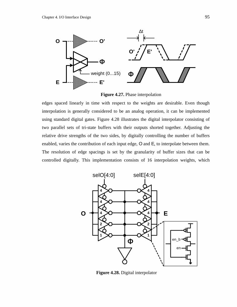
Chapter 4. I/O Interface Design 95
edges spaced linearly in time with respect to the weights are desirable. Even though
interpolation is generally considered to be an analog operation, it can be implemented
using standard digital gates. Figure 4.28 illustrates the digital interpolator consisting of
two parallel sets of tri-state buffers with their outputs shorted together. Adjusting the
relative drive strengths of the two sides, by digitally controlling the number of buffers
enabled, varies the contribution of each input edge, Ο and Ε, to interpolate between them.
The resolution of edge spacings is set by the granularity of buffer sizes that can be
controlled digitally. This implementation consists of 16 interpolation weights, which
O'
E'
ΦΦΦΦ
O
E
weight (0...15) ΦΦΦΦ
O' E'
∆t
Figure 4.27. Phase interpolation
1
2
4
4
4
1
2
4
4
4
EO
selE[4:0]selO[4:0]
en
en_bΦΦΦΦ
Figure 4.28. Digital interpolator

96 Chapter 4. I/O Interface Design
results in a total of 192 edge positions possible within a clock cycle, since there are 12
evenly spaced clock edges generated by the core DLL. In order to save area for these 16
interpolation steps, the weighting is binary coded for the lowest three bits. Thermometer
coding is used for the two higher order bits to avoid non-monotonic discontinuities that
can arise from full binary coding due to device width variations. It is important to
minimize, if not eliminate, non-monotonic discontinuities since it can directly translate
into jitter, where the loop dithers about that point.
The linearity of interpolated edges strongly depends on the ratio between the edge
spacing versus the output time constant of the interpolator. A measured histogram plot of
16 interpolations steps, generated by stepping though the interpolator in the test chip, is
presented in Figure 4.29. A slight nonlinearity shown in the plot is due to an improper
ratio of the interpolator’s output time constant to the input edge spacing. The capacitive
loading at the output of the interpolators is small and results in ∆t/RC = 2. ∆t is the delay
spacing between the interpolated edges, which is the delay of a single inverter in the delay
line of the core DLL. RC is the output time constant of the interpolators, set by the parallel
combination of the effective pull-up and pull-down resistances of the interpolator and the
capacitive load. A ratio closer to one yields better linearity, from the analysis described in
[44].
Figure 4.29. Measured interpolation histogram

Chapter 4. I/O Interface Design 97
In order for this interpolator to exhibit good linearity across a wide frequency range,
the ∆t/RC ratio must preserved. With an adaptively regulated supply, this ratio is constant
since the interpolator’s output time constant tracks with an inverter delay. Therefore, the
same linearity can be maintained over a wide range of frequencies with a simple digital
interpolator.
4.5.3 Duty-cycle adjuster
Another aspect of this timing block that requires careful design is the duty-cycle control.
The transmitter took special care to ensure that the bit time for data transmitted on both
phases of the clock were equal. Similarly, the duty cycle of Φ0 must be tightly controlled
in order for the receiver to accurately decipher the data encoded in each clock phase. Due
to skews in clock generation, an explicit duty-cycle adjusting block is necessary [28] and
is described next.
Applying duty cycle correction to full-swing CMOS signals presents a challenge for
implementing a duty-cycle adjustor (DCA). The basic approach, presented in Figure 4.30,
relies on static current to shift the switching threshold of inverters. Two sets of current
Figure 4.30. Duty-cycle adjuster schematic
clk clk
padjpadjnadjnadj
clknadj
padj padjclk
nadj
Vdd
RVdd
RVddRVdd
Vdd
clk_in
RVdd
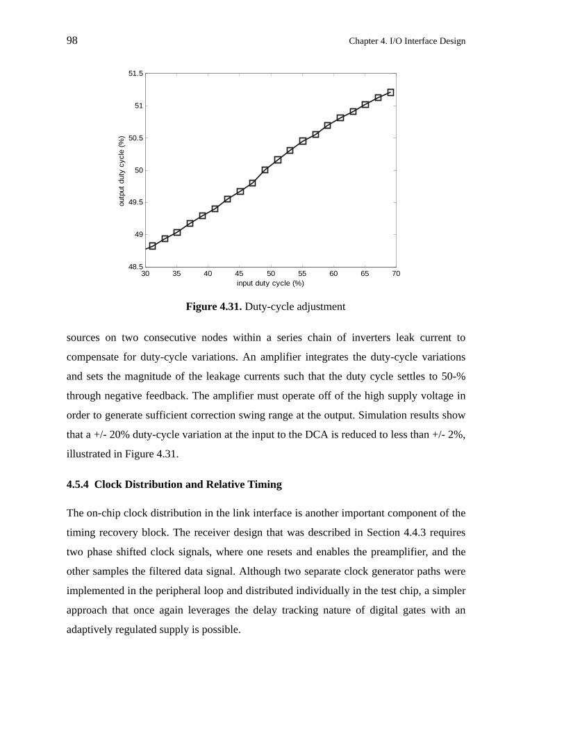
98 Chapter 4. I/O Interface Design
sources on two consecutive nodes within a series chain of inverters leak current to
compensate for duty-cycle variations. An amplifier integrates the duty-cycle variations
and sets the magnitude of the leakage currents such that the duty cycle settles to 50-%
through negative feedback. The amplifier must operate off of the high supply voltage in
order to generate sufficient correction swing range at the output. Simulation results show
that a +/- 20% duty-cycle variation at the input to the DCA is reduced to less than +/- 2%,
illustrated in Figure 4.31.
4.5.4 Clock Distribution and Relative Timing
The on-chip clock distribution in the link interface is another important component of the
timing recovery block. The receiver design that was described in Section 4.4.3 requires
two phase shifted clock signals, where one resets and enables the preamplifier, and the
other samples the filtered data signal. Although two separate clock generator paths were
implemented in the peripheral loop and distributed individually in the test chip, a simpler
approach that once again leverages the delay tracking nature of digital gates with an
adaptively regulated supply is possible.
30 35 40 45 50 55 60 65 7048.5
49
49.5
50
50.5
51
51.5
input duty cycle (%)
outp
utdu
tycy
cle
(%)
Figure 4.31. Duty-cycle adjustment

Chapter 4. I/O Interface Design 99
The peripheral loop enables the generation of the phase-shifted clock, Φ1, by utilizing
a secondary multiplexor-interpolator block whose edge selection and interpolation weight
is determined by adding a binary value equivalent to the desired relative phase spacing to
the output the FSM that sets Φ0. As a result, there is a fixed difference between the two
edges. We opted for this approach to generating the two edges in order to arbitrarily skew
the two clock edges to the receiver. However, a simpler approach is possible by locally
offsetting the sampler clock through a chain of inverters from Φ0, which alone is
distributed. Since the delay of each inverter is a fixed percentage of the clock period, a
locally generated Φ1 will always be phase shifted relative to Φ0 by a fixed percentage of
the clock period, thereby obviating the need for distributing additional clocks.
This delay tracking behavior also obviates clock retiming paths in the feedback path of
peripheral loop. Since the delay through the peripheral loop consists entirely of digital
gates, with a regulated supply, delay through the loop is again a fixed percentage of the
clock cycle and offers another advantage over traditional designs. If the input clock edges
to the interpolator happens to coincide with signals that control the mux and interpolator,
it can potentially glitch the output clock signal. In traditional designs, there is no known
relationship between the delay through the peripheral loop and clock frequency.
Therefore, traditional loops require explicit re-timing paths to avoid potential glitches that
can occur for different operating frequencies. However, with a regulated supply, delay
paths are a fixed percentage of the clock cycle and such conditions can be guaranteed to
never occur by construction and further simplifies the design.
4.5.5 Timing Recovery Summary
This section has described the timing recovery loop, which is an integral part of
high-speed link design. It relies on a dual-loop DLL architecture, where the core loop,
described in Section 4.2, not only sets the necessary regulated voltage level with respect to
the bit rate, but also generates evenly spaced clock edges to the peripheral loop. The
peripheral loop performs the actual clock recovery by aligning the internal clock signals
with respect to the incoming source synchronous clock and data. Fine clock edge
placement, down to 1/192 of the clock cycle, is possible through the multiplexor and

100 Chapter 4. I/O Interface Design
interpolator implementation. Furthermore, using the data receiver as a bang-bang phase
detector allows the clock path to match the data. Such precise clock alignment maximizes
timing margins for accurate data recovery.
As seen for the transmitter and receiver, an adaptively regulated supply offers several
advantages for implementing the peripheral loop. Previous implementations relied on
precision analog circuits to implement the multiplexor and interpolator in order to
interface to the analog delay elements in the core loop and to control the time constants of
devices in the interpolator with respect to operating frequency. By operating off of an
adaptively regulated supply, the supply voltage provides process, temperature, and timing
information. Therefore, a loop comprised almost entirely out of digital CMOS gates is
possible, simplifying its design. The interface between the core and peripheral loop is
trivial, because both sides consist of full-swing digital gates that operate at the same
voltage level. And even interpolation, normally considered an analog function, is
achievable with a parallel set of tri-state buffers. In addition, the delay tracking nature of
the digital gates obviates clock re-timing paths and offers further simplifications to clock
distribution by allowing the designer to accurately generate different clock phases locally.
4.6 Experimental Results
All of the components described so far have been implemented together and this section
describes the experimental results obtained from the test-chip prototype, which was
fabricated in a HP0.35µm CMOS10B NWELL process [50]. The section starts by
describing additional details of the test chip, mainly, the supporting test circuitry
incorporated to enable testing and to measure performance. Then, it presents the
performance characteristics and analysis of the dual-loop DLL and I/O transceiver.
Measured results of the power supply regulator were presented in Chapter 3 and is
therefore only summarized along with the rest of the chip’s overall performance. Lastly,
this section investigates the implications of this adaptive supply regulation technique on
power consumption.
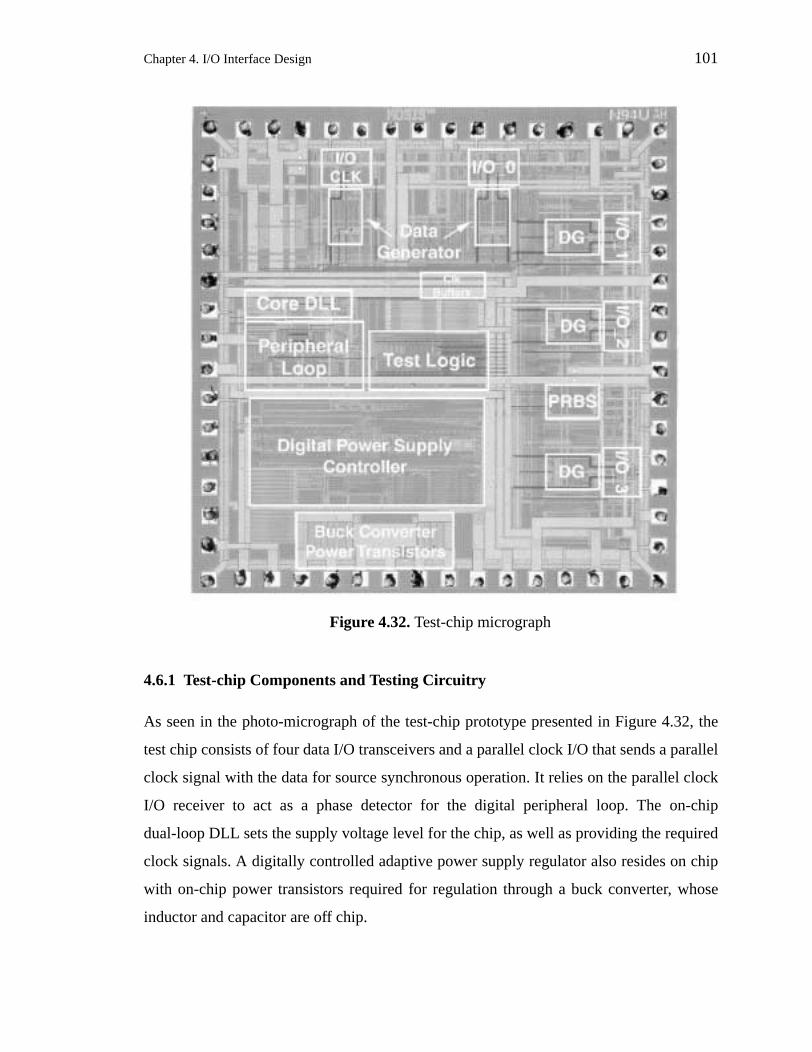
Chapter 4. I/O Interface Design 101
4.6.1 Test-chip Components and Testing Circuitry
As seen in the photo-micrograph of the test-chip prototype presented in Figure 4.32, the
test chip consists of four data I/O transceivers and a parallel clock I/O that sends a parallel
clock signal with the data for source synchronous operation. It relies on the parallel clock
I/O receiver to act as a phase detector for the digital peripheral loop. The on-chip
dual-loop DLL sets the supply voltage level for the chip, as well as providing the required
clock signals. A digitally controlled adaptive power supply regulator also resides on chip
with on-chip power transistors required for regulation through a buck converter, whose
inductor and capacitor are off chip.
Figure 4.32. Test-chip micrograph

102 Chapter 4. I/O Interface Design
Different test configurations for the chip is managed through a control block found in
the center of the test chip. There are 20 16-bit registers that are used to control the
different units. Configuration data is loaded in the chip by serially scanning in 16 bits of
data along with a 5-bit address. In addition, each transmitter has an 8-bit data pattern
generator that can be set through this interface to enable a variety of data sequences to test
proper functionality of the links. A 20-bit pseudo-random bit-sequence generator and
verifier also reside on the chip and is used to measure the bit-error rate (BER) of the link.
The use of 20 bits enables the links to be tested with wide spectral content, which is
important since there are no requirements for DC balancing or scrambling that would
normally be required in interface designs that do not have an explicit clock and therefore
require clock recovery from the incoming bit stream.
4.6.2 Dual-Loop DLL
The dual-loop DLL, on the left side of the chip micrograph, consists of the core and
peripheral blocks. The core DLL is supplied off of the high Vdd supply and operates from
33-500 MHz with corresponding regulated voltage settings ranging from 1.3-3.2 V as
plotted in Figure 4.33. The digital peripheral loop operates off of RVdd, set by the core
loop, and operates from 100-500 MHz. The receiver used as a phase detector for the
Figure 4.33. Regulated voltage vs. frequency
0
50
100
150
200
250
300
350
400
450
500
1 1.25 1.5 1.75 2 2.25 2.5 2.75 3 3.25
Fre
quen
cy(M
Hz)
RVdd (V)

Chapter 4. I/O Interface Design 103
peripheral loop resides in the link above the DLL block and limits the lower frequency
range of operation due to a minimum 1.3-V supply headroom required by the analog
preamplifier. Figure 4.34 shows the core and dual loop jitter histogram plots while running
at 400-MHz under quiet supply conditions. The larger jitter in the dual loop can be
attributed to the peripheral loop occasionally dithering between interpolation steps. Due to
a lack of on-chip supply noise generators, jitter measurements for the core loop under
noisy conditions could not be accurately measured. However, a PLL design that also
implements supply-controlled inverters as delay elements and a similar regulating
amplifier design, presented in [42], exhibits a measured power supply rejection ratio of 15,
and closely matches simulated results. Although the regulating amplifier actively rejects
and filters out power supply noise to reduce jitter in the core loop, the digital circuitry in
the peripheral loop has no such mechanism besides the peripheral loop. The peripheral
loop can compensate for delay variations due to low frequency supply variations below its
effective loop bandwidth and responds to supply steps with a time constant set by the
loop’s slew rate.
While operating at 400-MHz, the core loop dissipates 37-mW operating off the 3.3-V
supply and the digital logic for the peripheral loop, supplied with a 2.7-V regulated
Figure 4.34. DLL jitter histogram -- (a) core, (b) dual
(a) (b)

104 Chapter 4. I/O Interface Design
voltage, dissipates 19-mW. Table 4.1 summarizes the measured dual-loop DLL
characteristics. Figure 4.35 plots the power consumed by the core and peripheral DLL
blocks versus frequency. Given that the peripheral loop is dominated by digital logic, its
power consumption exhibits an almost cubed relation to frequency, whereas the core
loop’s power is super-linear with frequency Due to an unidentified static current path
Table 4.1. Dual-loop DLL performance summary
Operating Range
core 33 - 500 MHz
peripheral 100 - 500 MHz
Jitter
core loop 21-ps pk-pk
dual loop 36-ps pk-pk
Power
core (Vdd) 51-mW (3.3-V)
peripheral (RVdd) 28-mW (2.7-V)
Active Area 0.035-mm2
Figure 4.35. Dual-loop DLL power consumption vs. frequency
5
10
15
20
25
30
35
40
45
50
100 150 200 250 300 350 4000
5
10
15
20
25
30
Cor
e-lo
opP
ower
(mW
)
Per
iphe
ral-l
oop
Pow
er(m
W)
Frequency (MHz)
core (measured)
core (simulated)
peripheral (measured)
Chapter 4. I/O Interface Design 105
between Vdd and Gnd, the core DLL’s measured power consumption is much larger than
simulated results, shown by the dotted line. Therefore, the actual magnitude of power is
inaccurate, but both measured and simulated power numbers exhibit the same relationship
with respect to frequency.
4.6.3 I/O Transceiver
The I/O interface operating range is set by the peripheral loop and therefore successfully
operates from 100-MHz to 500-MHz, which translates to a 0.2-1 Gb/s range in bit rates
across a 1.3-3.2 V range in regulated voltage levels. The fabrication run for the test chip
turned out slower than expected from simulations, and therefore required a high Vdd
boosted to 3.7-V to comfortably meet the headroom requirements of the linear regulator in
the core DLL in order to operate at the high frequency target of 500-MHz. Transmitting
and receiving a 20-bit PRBS at a transfer rate of 0.8-Gb/s verifies a bit-error rate less than
10-14 (which corresponds to three days of operation without a single error). This test was
performed by transmitting and receiving signals between two chips through 8-inches of
50-Ω traces on FR4 printed circuit boards and 36-inch coax cables.
Figure 4.36 plots the total regulated power consumed per link operating across a range
of bit rates for single-ended and differential modes of operation to demonstrate the power
saving potential of dynamically scaling the supply to the I/O subsystem. Although a true
demonstration of the power savings possible requires a comparison between the same link
design operating off of a fixed supply versus a regulated supply, since the chip was
designed to only operate with a dynamically adjusted supply, experimental measurements
of the chip’s power consumption for a fixed supply voltage configuration was not
possible. However, the estimated power consumption of the overhead power operating off
of a fixed high supply voltage (3.3-V) was generated by calculating the effective switched
capacitance of the digital circuitry and applying it to the dynamic power equation with a
fixed supply voltage. It is presented by the dashed line in Figure 4.36 and emphasizes the
power saving potential of adaptively regulating the supply. Since the regulated voltage
varies with frequency, power consumption while operating off of a dynamically adjusted
supply reduces dramatically for lower bit rates. It is important to note that this estimated

106 Chapter 4. I/O Interface Design
power is for the same process corner as the chip that was tested and does not offer insight
into the potential power savings which can be achieved for different process corners and
operating conditions.
To compare single-ended signalling versus differential signalling, the overhead power
common to both configurations is identified by the dashed line and represents the power
consumed by the receiver and a portion of the power dissipated in the bias generator,
peripheral loop, clock distribution network, and testing circuitry amortized across all the
links. The difference between the total power and the overhead represents the power
dissipated in the transmitter at the minimum transmission swings achieved for different
transmission bit rates. The minimum transmission swings achieved versus bit rate are
plotted in Figure 4.37. Although differential signalling requires two parallel channels to
transmit data, they require less than half the swing magnitude compared to single-ended
signalling and hence consume less power. Noise on the reference voltage that is shared by
all the receivers is common-mode and adversely affects the voltage margins for the
receiver, thus requiring the larger swing magnitudes for single-ended signalling.
Therefore, from a system perspective, since there is little difference in power
300 400 500 600 700 8000
5
10
15
20
25
30
35
40
45
Pow
er/L
ink
(mW
)
Bit Rate (Mb/s)
single-endeddifferentialoverhead (var. Vdd)overhead (fixed Vdd)
Figure 4.36. Single-ended and differential link power vs. bit rate

Chapter 4. I/O Interface Design 107
consumption, the choice between single-ended and differential signalling would be
dictated by other factors such as pin resources available for the I/O interface or
communication distances which may require differential signalling.
An additional advantage of adaptively scaling the supply comes from the automatic
slew-rate control of the transmitter output. Figure 4.38 presents the measured data-eye
diagram for a PRBS data stream transmitted at 0.8-Gb/s. It verifies the 50-% duty-cycle
signals achieved by pre-distorting the predrivers to the output driver and shows the output
slews for a third of the bit time. This slew-rate control also extends to different
frequencies, demonstrated by the relatively constant rise and fall transition times as a
percentage of bit time, presented over a range of bit rates in Table 4.2.
200 300 400 500 600 700 800 9000
20
40
60
80
100
120
140
160
180
Min
imum
Tra
nsm
itter
Out
putS
win
g(m
V)
Bit Rate
differentialsingle-ended
Figure 4.37. Minimum transmission swing vs. bit rate
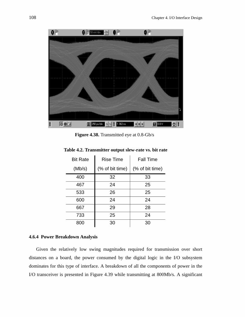
108 Chapter 4. I/O Interface Design
4.6.4 Power Breakdown Analysis
Given the relatively low swing magnitudes required for transmission over short
distances on a board, the power consumed by the digital logic in the I/O subsystem
dominates for this type of interface. A breakdown of all the components of power in the
I/O transceiver is presented in Figure 4.39 while transmitting at 800Mb/s. A significant
Table 4.2. Transmitter output slew-rate vs. bit rate
Bit Rate Rise Time Fall Time
(Mb/s) (% of bit time) (% of bit time)
400 32 33
467 24 25
533 26 25
600 24 24
667 29 28
733 25 24
800 30 30
Figure 4.38. Transmitted eye at 0.8-Gb/s

Chapter 4. I/O Interface Design 109
portion of the power is consumed by the clock distribution, clock recovery, and data
generators, while only 11-% is consumed by the transceiver itself. Therefore, this type of
I/O subsystem especially benefits from the savings possible by reducing the dynamic
power dissipated by digital gates with adaptive power supply regulation.
The test-chip prototype only contains 4 data links, but the measured results can be
extrapolated to understand the power implications of this approach for much wider
parallel I/O interfaces. The power consumption of each link grows linearly with each
additional link and so does much of the clock distribution power and supporting digital
circuitry that interfaces the links to the rest of the digital system. A component of power
that does not scale linearly with the number of links is the timing-recovery block.
Enabling more links to share a single timing recovery block reduces the overhead power
consumed per link. However, due to large skews that can potentially result for links spread
across a large die (both on the chip and on the board), multiple timing recovery blocks for
sets of links on different parts of the chips may be necessary. Furthermore, communication
with multiple chips utilizing this type of parallel interface requires multiple
timing-recovery blocks for each set of links communicating to different chips.
Figure 4.39. Power breakdown at 800Mb/s
core DLL23%
peripheral DLL14%
RX clk15%
TX clk28%
RX7%
TX4%
TX data9%

110 Chapter 4. I/O Interface Design
4.7 Summary
Running a high-speed parallel I/O interface off of an adaptively regulated supply voltage
provides several advantages. The process, temperature, and frequency information
embedded within the regulated supply, coupled with the delay tracking nature of digital
CMOS gates, leads to a simple design that minimizes precision analog circuits. A
predominantly digital design enables easier integration into large digital chips. In addition,
its power consumption scales not only with the environment, but also with the operating
frequency. The proposed interface optimizes power consumption by reducing margins
normally required in conventional, fixed-supply designs to cover all corner cases.
Furthermore, the I/O can trade performance for lower power. Consequently, a digital core
that can adaptively vary its I/O bit rate with respect to its communication bandwidth
requirements can significantly reduce power consumption. The test chip demonstrated that
cutting the bit rate down by one half reduced power consumption by a factor of 5.7. This is
all possible with a digitally-controlled power-supply regulator that can also be
implemented within the same die as the interface and the rest of the digital chip (except for
the off-chip inductor and capacitor).

111
Chapter 5
Conclusions
This dissertation has shown that a power reduction technique, referred to as adaptive
power supply regulation, is not only applicable to large digital cores, but can also be
effectively applied to a high-speed parallel I/O interface. It enables a simple and yet robust
design while facilitating efficient power consumption by tracking process variations,
environmental conditions and frequency. It relies on a performance monitoring circuit,
which in this case is a simple inverter, to map the relationship between circuit delay and
operating conditions. Given the strong correlation between supply voltage and circuit
delay, and dynamic power’s quadratic dependence on voltage, significant power reduction
is possible by eliminating voltage margins and operating circuits at the minimum voltage
required to guarantee timing. Dynamically regulating the supply voltage requires an
efficient power supply regulator to separately drive the I/O interface.
The ability to adaptively reduce supply voltage and still guarantee timing requirements
requires a circuit that can track the critical delay path in the I/O interface across all process
and operating conditions. In Chapter 2, an inverter was shown to be an effective delay
model that accurately tracks the delay of various static and dynamic gates across process
and temperature variations. Due to velocity saturation effects, tracking was not as good
across voltage. Therefore, the design of the delay tracking inverter becomes more critical
and in some cases may require voltage margins to guarantee timing across the entire
voltage range of operation. Designing a delay tracking circuit that consists of the same
types of gates that constitute the critical path minimizes these margins. While this may be
difficult to do in large digital blocks where delay paths are balanced as much as possible,
the critical path in the I/O interface conveniently consists of inverters that drive the clock

112 Chapter 5. Conclusions
distribution network. Therefore, inverters worked out to be the best fit.
Finding the “right” voltage for operation with respect to process, temperature, and
frequency is achievable in different ways. Chapter 2 described a digitally-controlled buck
converter that regulates the output voltage with respect to an input reference frequency.
And an inverter-based ring oscillator was used to model the critical path. For the I/O
interface, the core loop of a dual-loop DLL used a small linear regulator to determine the
“right” voltage required to match the delay through a chain of inverters to the input clock
period. An efficient regulator was then used to replicate this voltage and drive the rest of
the I/O interface.
Adaptively regulating the supply voltage not only offers power savings, but it can also
enable a simple I/O design that replaces many precision analog circuits with digital gates.
The regulated voltage contains information about the process and operating conditions for
the chip, so that the delay of gates tracks the frequency of operation. This has enabled
automatic slew-rate and output swing magnitude control for the transmitters and a
bandwidth tracking input receiver. The clock distribution network may also take
advantage of this property to locally generate necessary clock phases that are a delayed a
fixed percentage of the clock period.
Chapter 4 demonstrated a parallel I/O interface, fabricated in an HP0.35µm CMOS
process, that can achieve high speeds while consuming less power by adaptively
regulating its supply voltage. The lower supply doesn’t necessarily limit its performance
since the I/O interface normally is not the performance bottleneck in a large digital chip.
Instead, the interface trades its excess performance capabilities for lower power
consumption. This interface achieves a BER less than 10-14 while running at 800-Mb/s
and consuming less than 35-mW per link. Given a system that can throttle its
communication bandwidth with respect to performance needs, reducing the bit rate to
400-Mb/s lowered power consumption to less than 7-mW per link. The chip’s
performance is summarized in Table 5.1.
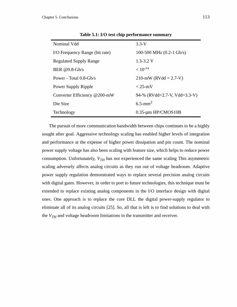
Chapter 5. Conclusions 113
The pursuit of more communication bandwidth between chips continues to be a highly
sought after goal. Aggressive technology scaling has enabled higher levels of integration
and performance at the expense of higher power dissipation and pin count. The nominal
power supply voltage has also been scaling with feature size, which helps to reduce power
consumption. Unfortunately, VTH has not experienced the same scaling This asymmetric
scaling adversely affects analog circuits as they run out of voltage headroom. Adaptive
power supply regulation demonstrated ways to replace several precision analog circuits
with digital gates. However, in order to port to future technologies, this technique must be
extended to replace existing analog components in the I/O interface design with digital
ones. One approach is to replace the core DLL the digital power-supply regulator to
eliminate all of its analog circuits [25]. So, all that is left is to find solutions to deal with
the VTH and voltage headroom limitations in the transmitter and receiver.
Table 5.1: I/O test chip performance summary
Nominal Vdd 3.3-V
I/O Frequency Range (bit rate) 100-500 MHz (0.2-1 Gb/s)
Regulated Supply Range 1.3-3.2 V
BER @0.8-Gb/s < 10-14
Power - Total 0.8-Gb/s 210-mW (RVdd = 2.7-V)
Power Supply Ripple < 25-mV
Converter Efficiency @200-mW 94-% (RVdd=2.7-V, Vdd=3.3-V)
Die Size 6.5-mm2
Technology 0.35-µm HP/CMOS10B

114 Chapter 5. Conclusions

115
References
[1] B.S. Amrutur, “Design and analysis of fast low power SRAMs,” Ph.D. dissertation,Stanford Univerisy, Stanford, CA, August 1999.
[2] G. Besten, “Embedded low-cost 1.2Gb/s inter-IC serial data link in 0.35mm CMOS,”IEEE Int’l Solid-State Circuits Conf. Dig. Tech. Papers, Feb. 2000, pp. 250-251.
[3] T. Burd, et. al., “A dynamic voltage scaled microprocessor system,” IEEE Int’lSolid-State Circuits Conf. Dig. Tech. Papers, Feb. 2000, pp. 294-295.
[4] T. Burd, et. al., “Processor design for portable systems,” Journal of VLSI SignalProcessing., vol. 13, no. 2-3, Aug.-Sept. 1996, pp. 203-221.
[5] A. P. Chandrakasan, et. al., “Data driven signal processing: An approach for energyefficient computing,” IEEE Int’l Symposium on Low Power Electronics and DesignDig. Tech. Papers, Aug. 1996, pp. 347-352.
[6] A.P. Chandrakasan, et. al., Low Power Digital CMOS Design. Norwell, MA: KluwerAcademic, 1995.
[7] W.J. Dally, et. al,. “Transmitter equalization for 4-Gbps signalling” IEEE Micro,Jan.-Feb. 1997. vol.17, no.1, p. 48-56
[8] A. Dancy, et. al, “Techniques for aggressive supply voltage scaling and efficientregulation,” Proceedings of the IEEE Custom Integrated Circuits Conf., May 1997,pp. 579-586.
[9] A. DeHon, et. al., “Automatic impedance control,” 1993 IEEE Int’l Solid-StateCircuits Conf. Dig. Tech. Papers, p. 164-5, Feb. 1993.
[10] D. Dobberpuhl, “The design of a high performance low power microprocessor,”IEEE Int’l Symposium on Low Power Electronics and Design Dig. Tech. Papers,Aug. 1996, pp. 11-16.
[11] K. Donnelly, et. al., “A 660 MB/s interface megacell portable circuit in0.3um-0.7mm CMOS ASIC,” IEEE Int’l Solid-State Circuits Conf. Dig. Tech.Papers, pp. 290-291, Feb 1996.

116 References
[12] R. Farjad-Rad, et. al., "A 0.3-µm CMOS 8-GS/s 4-PAM Serial Link Transceiver",IEEE Symposium on VLSI Circuits Dig. Tech. Papers, p. 41-44
[13] M. Fukaishi, et. al., “A 20Gb/s CMOS multi-channel transmitter and receiver chipset for ultra-high resolution digital display,” IEEE Int’l Solid-State Circuits Conf.Dig. Tech. Papers, Feb 2000, pp. 260-261.
[14] R. Gu, et. al., “ 0.5-3.5Gb/s low-power low-jitter serial data CMOS transceiver,”IEEE Int’l Solid-State Circuits Conf. Dig. Tech. Papers, Feb 1999, pp. 352-353.
[15] V. Gutnik, et. al., An efficient controller for variable supply voltage low powerprocessing,” IEEE Symposium on VLSI Circuits Dig. Tech. Papers, June 1996, pp.158-159.
[16] R. Ho, et. al., “Interconnect scaling implications for CAD,” IEEE/ACM Int’l Conf.Computer Aided Design Dig. Tech. Papers, Nov. 1999, pp. 425-429.
[17] P. Hofstee, et. al., “A 1GHz single-issue 64b PowerPC processor,” IEEE Int’lSolid-State Circuits Conf. Dig. Tech. Papers, Feb. 2000, pp. 92-93.S.
[18] M. Horowitz, “Low power processor design using self-clocking,” Workshop onLow-Power Electronics, 1993.
[19] M. Horowitz, et. al., “High-speed electrical signalling: Overview and limitations,”IEEE Micro, vol. 18, no. 1, Jan.-Feb. 1998, pp.12-24.
[20] C. Hu, “Future CMOS scaling and reliability,” Proceedings of IEEE, Vol. 81, no.5,May 1993, invited paper.
[21] A. Jain, et. al., “A 1.2GHz Alpha microprocessor with 44.8GB/s chip pinbandwidth,” IEEE Int’l Solid-State Circuits Conf. Dig. Tech. Papers, Feb. 2001, pp.240-241.
[22] D. Jeong, et. al., “Design of PLL-based clock generation circuits,” IEEE Journal ofSolid-State Circuits, vol. 22, no.2, April 1987, pp. 244-261.
[23] M. Johnson, “Bias circuit and differential amplifier having stabilized output swing,”US Patent 5452898, Sept. 1995.
[24] J.G. Kassakian, et. al. “High-frequency high-density converters for distributed powersupply systems, Proceedings of the IEEE, vol. 76, no. 4, 1988.
[25] J. Kim, “A digital adaptive power-supply regulator using sliding control,” IEEESymposium on VLSI Circuits Dig. Tech. Papers, June 2001.
[26] B. Lau, et. al., “A 2.6Gb/s multi-purpose chip to chip interface,” IEEE Int’lSolid-State Circuits Conf. Dig. Tech. Papers, Feb 1998, pp. 162-163.
[27] J. Lee, “A low-noise fast-lock phase-locked loop with adaptive bandwidth control,”IEEE Journal of Solid-State Circuits, vol. 35, no. 8, Aug. 2000, pp. 1137-1145.

References 117
[28] T.H. Lee, et. al., “A 2.5V CMOS delay-locked loop for 18Mbit, 500megabyte/sDRAM,” IEEE Journal of Solid-State Circuits, vol. 29, no. 12, Dec. 1994, pp.1491-1496.
[29] P. Maken, M. Degrauwe, M. Van Paemel and H. Oguey, “A voltage reductiontechnique for digital systems,” IEEE Int’l Solid-State Circuits Conf. Dig. Tech.Papers, Feb. 1990, pp238-239.
[30] J.G. Maneatis, “Low-Jitter process independent DLL and PLL based on self-biasedtechniques,” IEEE Journal of Solid-State Circuits, vol. 28, no. 12, Dec. 1993.
[31] J.G. Maneatis, “Precise delay generation using coupled oscillators,” Ph.D.dissertation, Stanford University, Stanford, CA, June 1994.
[32] D. Monticelli, “Switching power supply design,” Proceedings of IEEE Symposiumon Low Power Electronics, Oct. 1995, p. 64.
[33] R.S. Muller, et. al., Device electronics for integrated circuits, John Wiley and Sons,1986.
[34] W. Namkoong, et. al., “A high-efficiency variable-voltage CMOS dynamic dc-dcswitching regulator,” IEEE Int’l Solid-State Circuits Conf. Dig. Tech. Papers, Feb.1997.
[35] L. Nielsen, et. al., “Low-power operation using self-timed circuits and adaptivescaling of supply voltage,” IEEE Trans. VLSI Syst., vol. 2, pp 391-397, Dec 1994.
[36] H. Notani, “A 622-MHz CMOS PLL with precharge-type phase frequencydetector,” IEEE VLSI Symp. Dig. Tech. Papers, Feb. 1994, pp. 129-130.
[37] E. Reese, et. al. “A phase-tolerant 3.8 GB/s data-communication router formuli-processor super computer backplane,” IEEE Int’l Solid-State Circuits Conf.Dig. Tech. Papers, pp. 296-297, Feb. 1994.
[38] S. Sakayima, et. al., “A lean power management technique: The lowest powerconsumption for the given operating speed of LSI’s,” IEEE Symposium on VLSICircuits Dig. Tech. Papers, June 1997, pp. 99-100.
[39] T. Sakurai, et. al., “Alpha-power law MOSFET model and its applications to CMOSinverter delay and other formulas,” IEEE Journal of Solid-State Circuits, vol. 25, no.2, April 1990, pp. 584-594.
[40] S. Sidiropoulos, et. al., “A 700-Mb/s/pin CMOS signalling interface using currentintegrating receivers,” IEEE Journal of Solid-State Circuits, May 1997, pp. 681-690.
[41] S. Sidiropoulos, et. al., “A CMOS 500Mbps/pin synchronous point to pointinterface,” IEEE Symposium on VLSI Circuits, June 1994.
[42] S. Sidiropoulos, et. al., “Adaptive bandwidth DLL’s and PLL’s usingregulated-supply CMOS buffers,” IEEE Symposium on VLSI Circuits Dig. Tech.Papers, June 2000.
118 References
[43] S. Sidiropoulos and M. Horowitz, “A semi-digital dual delay-locked loop,” IEEEJournal of Solid-State Circuits, Nov. 1997, pp. 1683-1692.
[44] S. Sidiropoulos, “High performance inter-chip signalling,” Ph.D. Dissertation,Stanford University, Stanford, CA, June 1998.
[45] A.J. Stratakos, “High-efficiency low-voltage DC-DC conversion for portableapplications,” Ph.D. dissertation, University of California, Berkeley, CA, Dec. 1998.
[46] K. Suzuki, et. al., “A 300 MIPS/W RISC core processor with variablesupply-voltage scheme in variable threshold-voltage CMOS,” Proceedings of theIEEE Custom Integrated Cicruits Conference, May 1997, pp. 587-590.
[47] T. Tanahashi, et. al., “A 2Bb/s 21CH low-latency transceiver circuit forinter-processor communication,” IEEE Int’l Solid-State Circuits Conference Dig.Tech. Papers, Feb. 2001, pp. 60-61.
[48] G. Wei, et. al. “A low power switching power supply for self-clocked systems,”IEEE Symposium on Low Power Electronics, Oct. 1996, pp. 313-317.
[49] G. Wei, et. al., “A full-digital, energy-efficient adaptive power supply regulator,”IEEE Journal of Solid-State Circuits, vol. 34, no. 4, April 1999, pp. 520-528.
[50] G. Wei, et. al., “A variable-frequency parallel I/O interface with adaptivepower-supply regulation,” IEEE Journal of Solid-State Circuits, vol. 35, no. 11, Nov.2000, pp. 1600-1610.
[51] C.K. Yang, “Design of high-speed serial links in CMOS,” Ph.D. dissertation,Stanford University, Stanford, CA, Decemeber 1998.
[52] K. Yang, “A scalable 32Gb/s parallel data transceiver with on-chip timingcalibration circuits,” IEEE Int’l Solid-State Circuits Conf. Dig. Tech. Papers, Feb.2000, pp. 258-259.
[53] E. Yeung, et. al., “A 2.4Gb/s/pin simultaneous bidirectional parallel link with per pinskew compensation,” IEEE Int’l Solid-State Circuits Conf. Dig. Tech. Papers, Feb.2000, pp. 256-257.
[54] P. Yue, “On-chip spiral inductors for silicon-based radio-frequency integratedcircuits,” Ph.D. dissertation, Stanford University, Stanford, CA, July 1998.
[55] J. Zerbe, et. al., “A 2Gb/s/pin 4-PAM parallel bus interface with transmit crosstalkcancellation, equalization, and integrating receivers,” IEEE Int’l Solid-State CircuitsConf. Dig. Tech. Papers, Feb. 2001, pp. 66-67.