ene 311 lecture 7. p-n junction a p-n junction plays a major role in electronic devices. it is used...
TRANSCRIPT

ENE 311 Lecture 7
p-n Junction
• - A p n junction plays a major role in electroni c devices.
• It is used in rectification, switching, and etc.
• It is the simplest semiconductor devices.
• Also, it is a key building block for other elect ronic, microwave, or photonic devices.

Basic fabrication steps
The basic fabrication steps for p-n junction inc lude
• oxidation,
• lithography,
• diffusion or ion implanation,
• and metallization.

Basic fabrication steps
• -This process is to make a high qu ality silicon dioxide (SiO
2 ) as an in
sulator in various devices or a bar rier to diffusion or implanation dur ing fabrication process.
• There are two methods to grow SiO2
: dry and wet oxidation, using d ry oxygen and water vapor, respe
ctively.
• Generally, dry oxidation is used t o form thin oxides because of its g
- ood Si SiO2 interface characteristi cs, while wet oxidation is used for
forming thicker layers since its hi gher growth rate.
Oxidation

Basic fabrication steps
• This process is calle d photolithography
used to delineate th - e pattern of the p n
junction.
Lithography
Basic fabrication steps
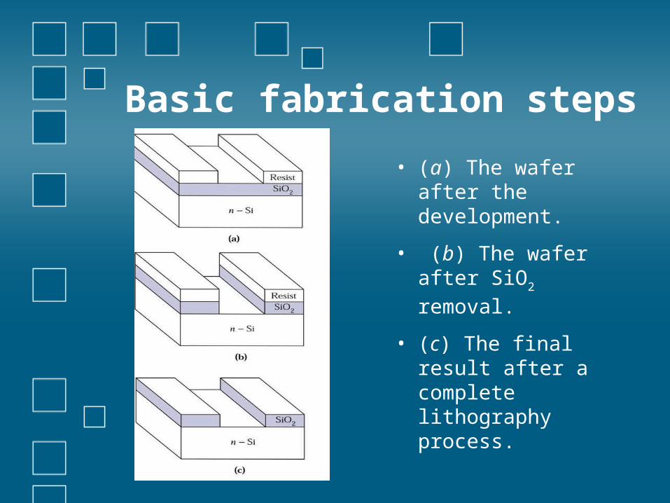
• (a) The wafer after the development.
• (b) The wafer after SiO2 removal.
• (c) The final result after a complete lithography process.

Basic fabrication steps• This is used to put the impurity int
o the semiconductor.
• For diffusion method, the semicon ductor surface not protected by th
e oxide is exposed to a high conce ntration of impurity. The impurity
-moves into the crystal by solid sta te diffusion.
• - For the ion implantation method, the impurity is introduced into the
semiconductor by accelerating th - e impurity ions to a high energy le
vel and then implanting the ions i n the semiconductor.
Diffusion & Ion Implantation

Basic fabrication steps
• This process is used to form ohmic cont
acts and interconne ctions.
• After this process is - done, the p n juncti
on is ready to use.
Metallization

Thermal equilibrium condition
• The most important charac - teristic of p n junction is re
ctification.
• The forward biased voltag e is normally less than1 V
and the current increases r apidly as the biased voltag
e increases.
• As the reverse bias increas es, the current is still small
until a breakdown voltage i s reached, where the curre nt suddenly increases.

Thermal equilibrium condition
• Assume that both p- and n-type semiconductors are uniformly doped.
• The Fermi level EF is near the valence band edge in the p-type material and near the conduction band edge in the n-type material.

Thermal equilibrium condition
• -Electrons diffuse from n sid - e toward p side and holes di
- -ffuse from p side toward n si de.
• -As electrons leave the n sid e, they leave behind the pos
itive donor ions (ND+ ) near t
he junction.
• In the same way, some of n egative acceptor ions (NA
- ) a re left near the junction as h
-oles move to the n side.

Thermal equilibrium condition
• This forms2 region s called “neutral ” r
egions and “ -spacecharge ” region.
• - The space charge r egion is also called
“ depletion region ” due to the depletio
n of free carriers.
Space-charge region
neutral neutral

Thermal equilibrium condition
• Carrier diffusion induc es an internal electric f
ield in the opposite dir ection to free charge d
iffusion.
• Therefore, the electron diffusion current flows
from left to right, wher eas the electron drift c
urrent flows from right to left.
Thermal equilibrium condition
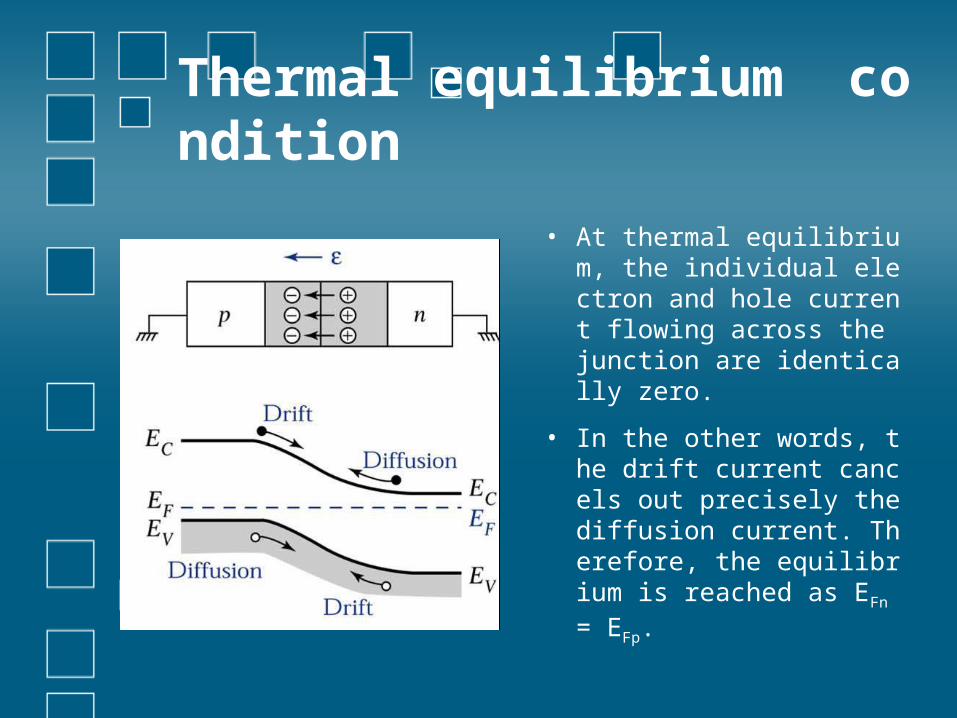
• At thermal equilibrium, the individual electron and hole current flowin
g across the junction a re identically zero.
• In the other words, the drift current cancels o
ut precisely the diffusi on current. Therefore, the equilibrium is reac hed as EFn = EFp.

Thermal equilibrium condition
• - The space charge density distribution and t he electrostatic potential are given by Poi
sson’s equation as
(1)
• Assume that all donor and acceptor atoms a re ionized.
2
2 D A
d dE eN N p n
dx dx

Thermal equilibrium condition
• Assume NA = 0 and n >> p for n-type neutral region and ND = 0 and p >> n for p-type neutral region.

Thermal equilibrium condition
• The electrostatic potential in of the n- and p-type with respect to the Fermi level can be found with the help of and
as
(2)
(3)
exp /i F in n E E kT
exp /i i Fp n E E kT
ln Dn F i
i
kT NE E
e n
ln Ap i F
i
kT NE E
e n

Thermal equilibrium condition
• The total electrostatic potential difference b - - etween the p side and the n side neutral reg
ion is called the “ - built in potential ” Vbi . It is written as
(5)2
ln A Dbi n p
i
kT N NV
e n

• a ) A -p n junction with a brupt doping changes a
t the metallurgical junction.
• (b ) Energy band diagra m of an abrupt junction at thermal equilibrium.
• (c ) Space charge distribution.
• (d ) Rectangular approxi mation of the space ch
arge distribution.

Thermal equilibrium condition
Ex. - Calculate the built in potential for a silicon- p n junction with NA = 1018cm-3 and ND =
1015 cm-3 at 300 K.

Ex. - Calculate the built in potential for a silicon- p n junction with NA = 1018cm-3 and ND =
1015 cm-3 at 300 K.
Soln
Thermal equilibrium condition
2
18 15
29
ln
10 100.0259ln
9.65 10
0.774 eV
A Dbi
i
bi
N NV kT
n
V
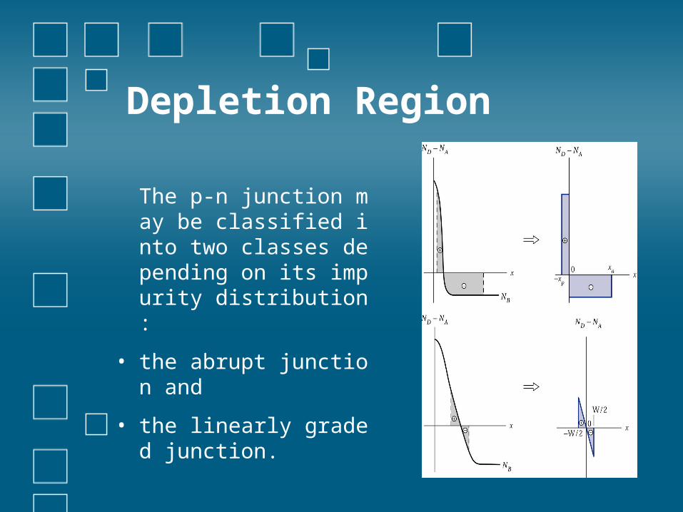
Depletion Region
- The p n junction ma y be classified into t
wo classes dependin g on its impurity dist
ribution:
• the abrupt junction a nd
• the linearly graded j unction.

Depletion Region
• An abrupt junction can b - e seen in a p n junction t
hat is formed by shallow - diffusion or low energy i
on implantation.
• The impurity distribution in this case can be appro
ximated by an abrupt tr ansition of doping conce - ntration between the n
- and the p type regions.
Depletion Region
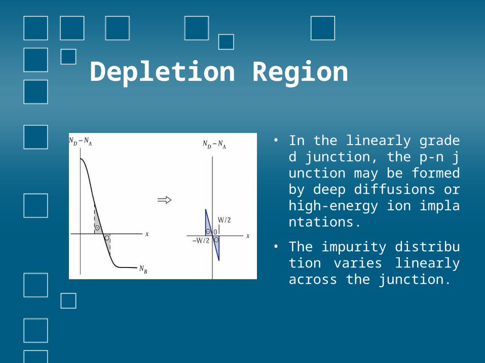
• In the linearly graded j - unction, the p n junctio
n may be formed by de -ep diffusions or high e
nergy ion implantation s.
• The impurity distributi on varies linearly acros
s the junction.

Abrupt junction • Consider an abrupt junctio
n as in the figure above, eq uation (1 ) can be written as
• The charge conservation is expressed by the condition Q = 0 or
2
2
2
2
for - 0
for 0
Ap
Dn
d eNx x
dx
d eNx x
dx
A p D nN x N x

Abrupt junction
• To solve equation (5), we need to solve it separately for p- and n-type cases.
-p side: Integrate eq.(4) once, we have
We know that
( )
A
A
p
d eN xc
dx
dE
dx
eN xE x c

Abrupt junction
Apply boundary condition: ( ) 0
( )( ) 0
p p
A p
p p
A p
E x x
eN xE x c
eN xc
( )( ) A pp
eN x xE x
(7)

Abrupt junction
-n side:
• Similarly, we can have
(8)
( )( ) D n Dn m
eN x x eN xE x E

Abrupt junction
• Let consider at x = 0
(9)
We may relate this electric field E to the poten tial over the depletion region as
( )(0) (0) A p D np n m
eN x eN xE E E
0
0
( ) ( ) ( )n n
p p
x x
bi
x x n sidep side
V E x dx E x dx E x dx

Abrupt junction
• From (6 ), we have
(11)
2 2
2 2A p D n
bi
eN x eN xV
A pn
D
D np
A
N xx
N
N xx
N
(10)

Abrupt junction
• Substitute (11 ) into (10 ), this yields
(12)
2
2
bi Dp
A D A
bi An
A D D
V Nx
e N N N
V Nx
e N N N

Abrupt junction
• - Hence, the space charge layer width or depl etion layer width can be written as
(13)
2 bi A Dp n
A D
V N NW x x
e N N

Abrupt junction
Ex. - Si p n diode of NA =5 x 1016 cm-3 and ND =1015 cm-3 . Calculate
- (a) built in voltage
(b) depletion layer width
(c) Em

Abrupt junction
Soln (a)
2
16 15
210
ln
5 10 100.0259ln
1.45 10
0.679 eV
A Dbi
i
bi
kT N NV
e n
V

Abrupt junction
Soln (b)
14 16 15
19 16 15
From (13)
2
2 8.85 10 11.8 0.679 5 10 10
1.6 10 5 10 10
0.95 m
bi A D
A D
V N NW
e N N
W
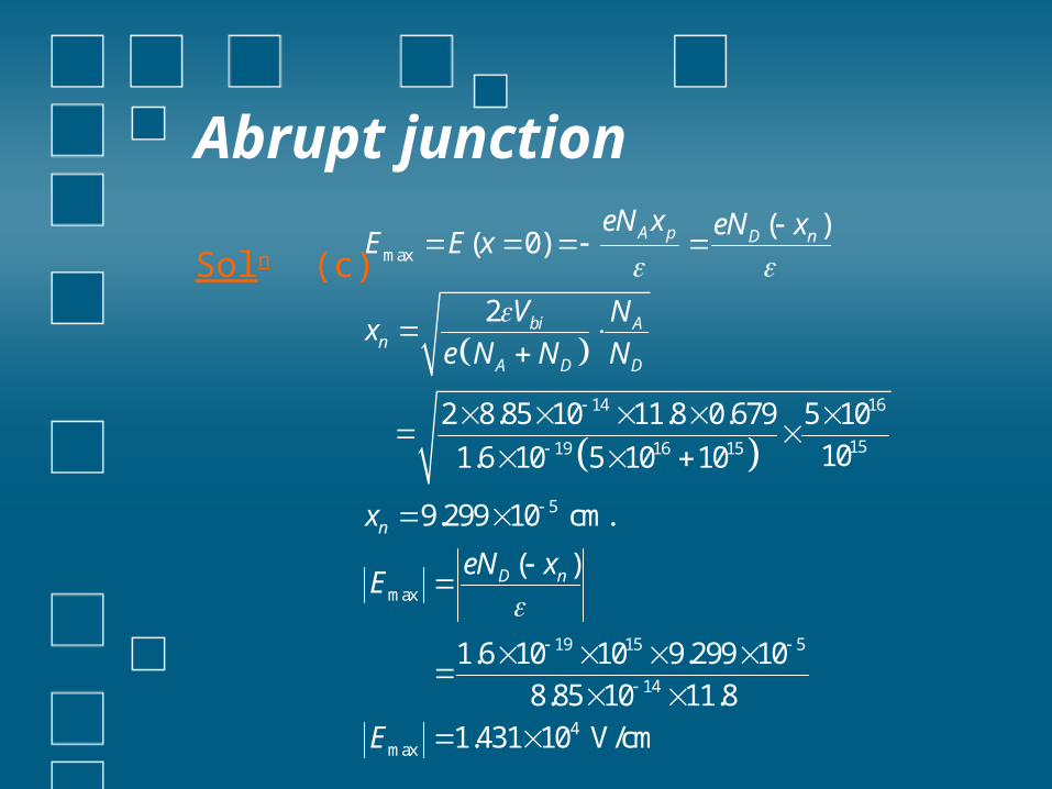
Abrupt junction
Soln (c)
max
14 16
1519 16 15
5
max
19 15 5
14
4max
( )( 0)
2
2 8.85 10 11.8 0.679 5 10
101.6 10 5 10 10
9.299 10 cm.
( )
1.6 10 10 9.299 10
8.85 10 11.8
1.431 10 V/cm
A p D n
bi An
A D D
n
D n
eN x eN xE E x
V Nx
e N N N
x
eN xE
E

Abrupt junction
• If one side has much higher impurity doping concentration than another, i.e. NA >> ND or ND >> NA, then this is called “one-sided junction”.
• Consider case of p+- n ju nction as in the figure (
NA >> ND), 2 bin
D
VW x
eN
Abrupt junction
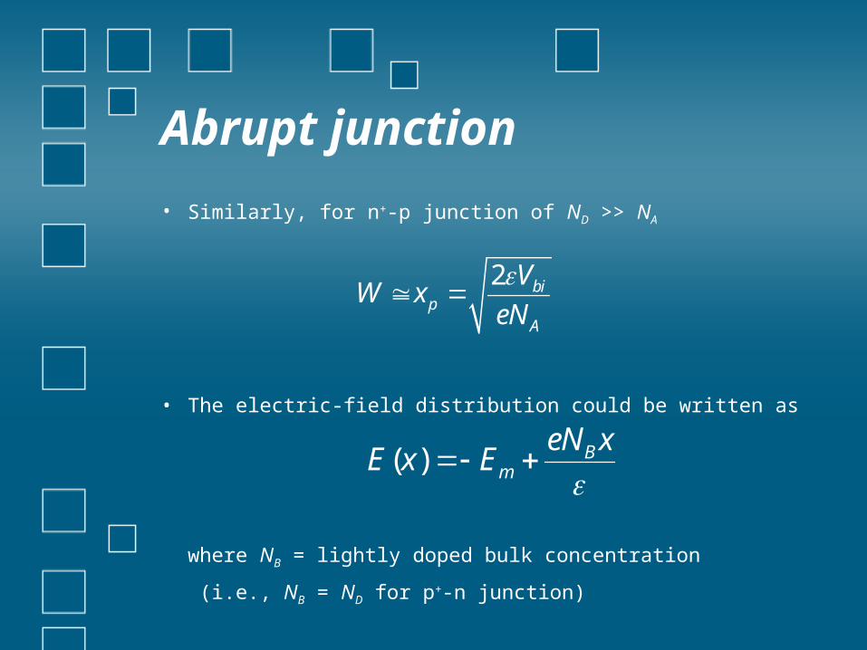
• Similarly, for n+- p junction of ND >> NA
• - The electric field distribution could be written as
where NB = lightly doped bulk concentration
(i.e., NB = ND for p+- n junction)
2 bip
A
VW x
eN
( ) Bm
eN xE x E

Abrupt junction
• The maximum electric field Em at x =0 can b e found as
• - Therefore, the electric field distribution E(x) - can be re written as
(16)
Bm
eN WE
( ) 1Bm
eN xE x W x E
W
Abrupt junction
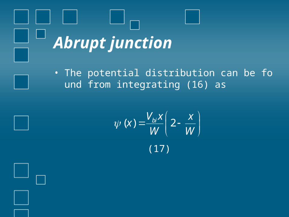
• The potential distribution can be found from integrating (16 ) as
(17)
( ) 2biV x xx
W W

Abrupt junction
Ex. - For a silicon one sided abrupt junction wit h NA = 1019 cm-3 and ND = 1016 cm-3 , calculat e the depletion layer width and the maximu m field at zero bias.

Abrupt junction
Soln
19 16
29
5
4
10 100.0259ln 0.895 V
9.65 10
23.41 10 0.343 m
0.52 10 V/cm
bi
bi
D
Bm
V
VW
eN
qN WE
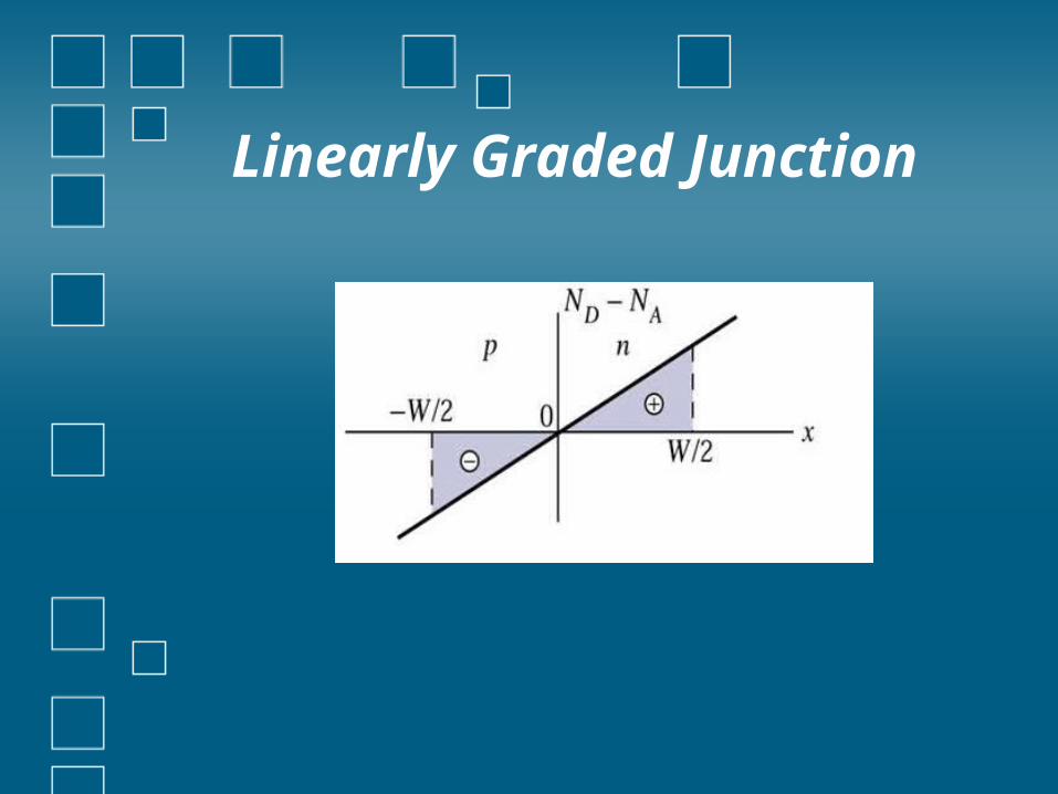
Linearly Graded Junction
Linearly Graded Junction
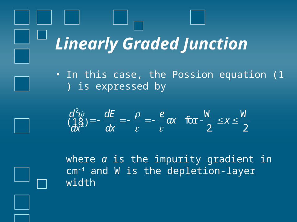
• In this case, the Possion equation (1 ) is expr essed by
(18)
where a is the impurity gradient in cm-4 and W is the depletion-layer width
2
2
W W for -
2 2
d dE eax x
dx dx
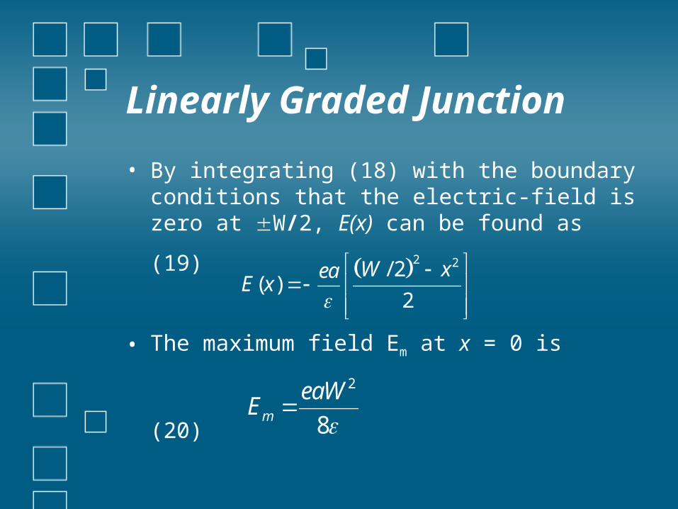
Linearly Graded Junction
• By integrating (18 ) with the boundary conditio - ns that the electric field is zero at W/2 , E(x) c an be found as
(19)
• The maximum field Em at x = 0 is
(20)
2 2/ 2( )
2
W xeaE x
2
8m
eaWE
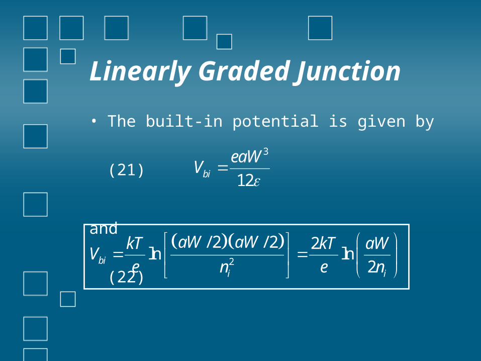
Linearly Graded Junction
• - The built in potential is given by
(21)
and
(22)
3
12bi
eaWV
2
/ 2 / 2 2ln ln
2bii i
aW aWkT kT aWV
e n e n

Linearly graded junction in thermal equilibrium.
(a) Impurity distribution. (b) Electric-field distribution.
(c) Potential distribution with distance.
(d) Energy band diagram.

Linearly Graded Junction
Ex. For a silicon linearly graded junction with a n impurity gradient of 1020 cm-4 , the depletio- n layer width is 0.5 μm. Calculate the maxi
- mum field and built in voltage.

Linearly Graded Junction
Soln
Note: Practically, the Vbi is smaller than that c alculated from (22 ) by about 0.05 to 0.1 V.
219 20 423
14
20 4
9
1.6 10 10 0.5 104.75 10 V/cm
8 8 11.9 8.85 10
2 10 0.5 102 0.0259 0.645 V
2 2 9.65 10
m
bii
eaWE
kT aWV
e n