emphasis, equalization & embedding · emphasis cleaning the rusty channel emphasis,...
TRANSCRIPT

Cleaning the Rusty Channel
Emphasis, Equalization & Embedding
Cleaning The Rusty ChannelEmphasis, Equalization & Embedding Page 1
Dr. Thomas KirchnerSenior Application EngineerDigital Debug Tools
Gustaaf Sutorius
Application Engineer
Agilent Technologies
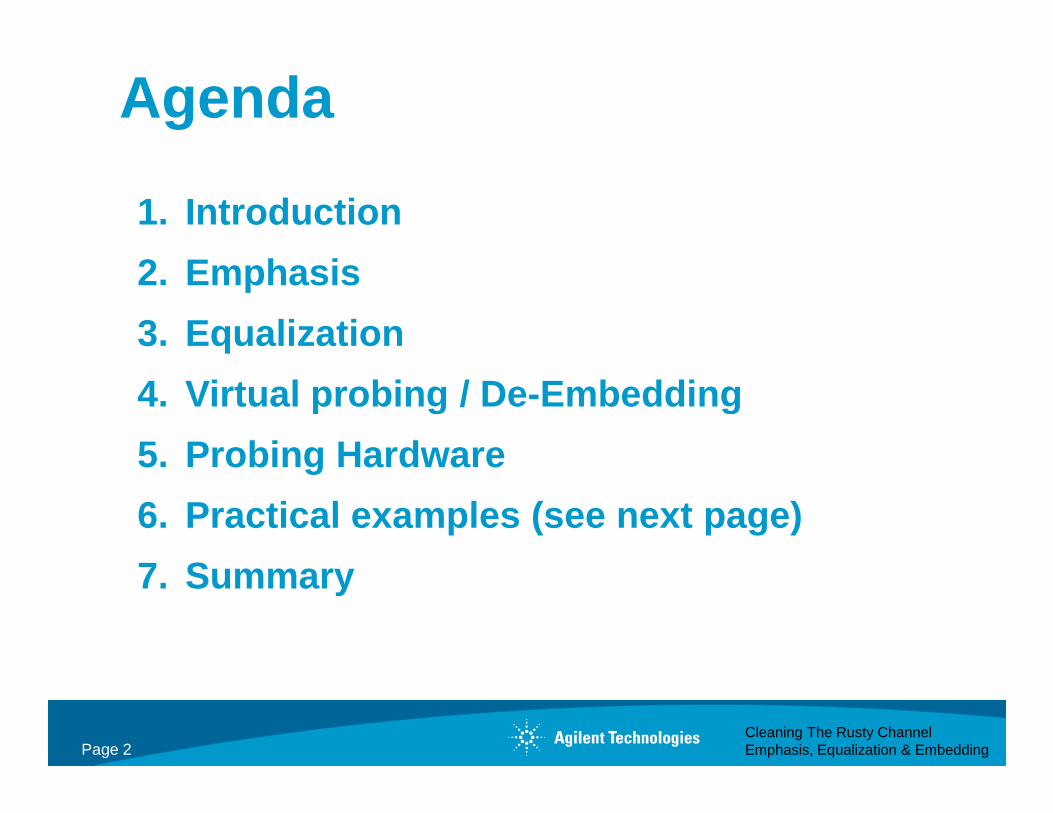
Agenda
1. Introduction
2. Emphasis
3. Equalization
4. Virtual probing / De-Embedding
Cleaning The Rusty ChannelEmphasis, Equalization & Embedding
4. Virtual probing / De-Embedding
5. Probing Hardware
6. Practical examples (see next page)
7. Summary
Page 2

Agenda continued6. Practical Examples
1. High-Speed Characterization (effect of 4.5 GHz Notch in test fixture)
2. BGA probe setup in infiniisim Virtual Probe
3. Tuned, measurement enhanced, IBIS parameters for DDR
Cleaning The Rusty ChannelEmphasis, Equalization & Embedding
DDR
4. Creating S2P (touchstone) files from Gerber files
5. Basic Steps for Optimizing a Serial Link
6. Serial Data Analysis Solutions: 8b10b Trigger, Decode, Search and Listing Feature
7. Small peek inside the 90.000 X 32 GHz scope
Page 3

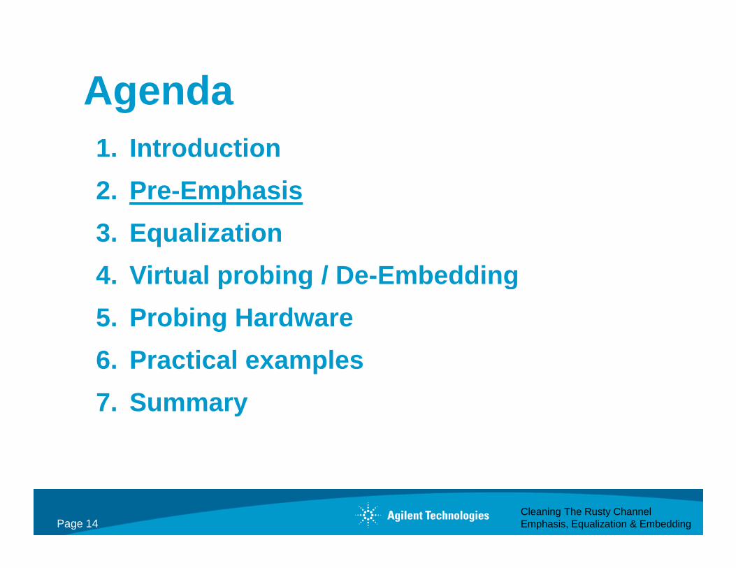
Agenda
1. Introduction2. Pre-Emphasis
3. Equalization
4. Virtual probing / De-Embedding
Cleaning The Rusty ChannelEmphasis, Equalization & Embedding
4. Virtual probing / De-Embedding
5. Probing Hardware
6. Practical examples (see next page)
7. Summary
Page 4

Generic Trend: Rates Going Higher & Higher
5G
10G
PCIe 2.0
PCIe 3.0
SATA3
USB3
• PCI Express
2.5 GT/s (2.0) 5 GT/s (3.0) 8 GT/s
• USB TechnologiesUSB 2.0 480MbpsWUSB (RF 3.1-10.6Ghz)USB 3.0 5GT/s
• SATA
DP1.2
5G
2006 2007 2008 2009
PCIe 1.1
SATA2
USB2WUSB
USB3
HDMI 1.3
2010
• SATA 1.5Gbps 3Gbps 6Gbps
• HDMI 1.3 3.4Gbps
• DisplayPort 2.7 Gbps 5.4Gbps
DP1.1
Page 5
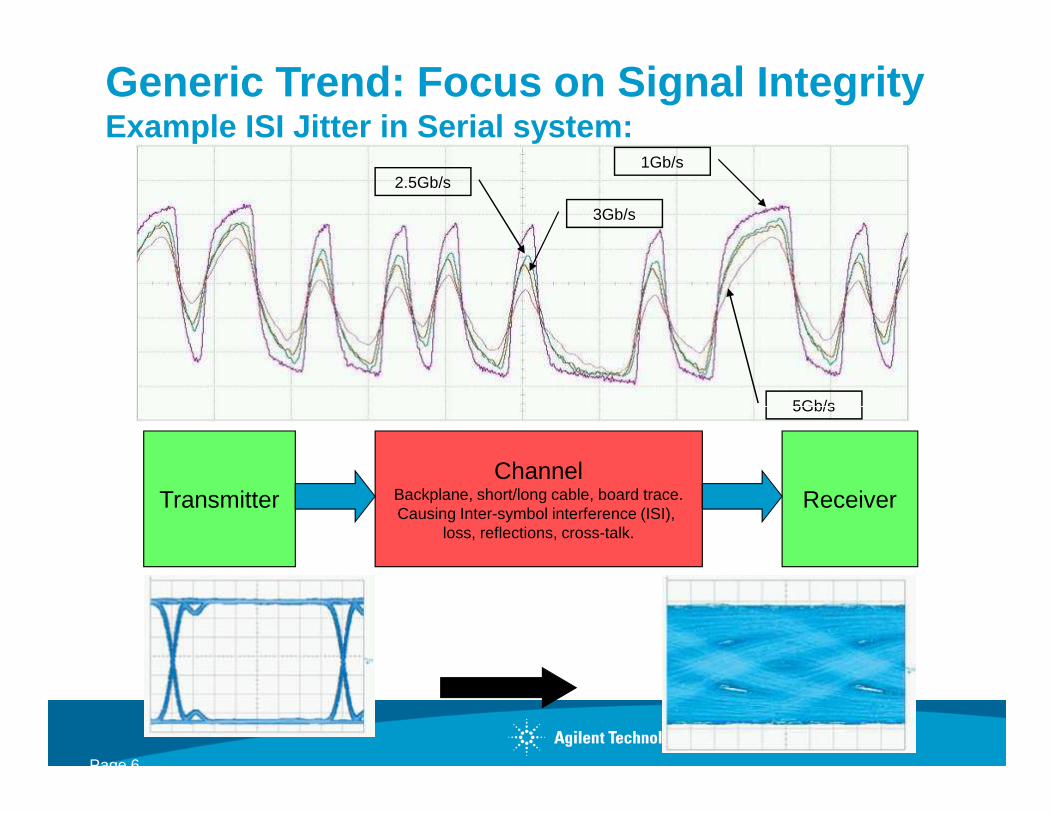
Generic Trend: Focus on Signal IntegrityExample ISI Jitter in Serial system:
1Gb/s
5Gb/s
2.5Gb/s
3Gb/s
TransmitterChannel
Backplane, short/long cable, board trace.Causing Inter-symbol interference (ISI),
loss, reflections, cross-talk.
Receiver
5Gb/s
Page 6
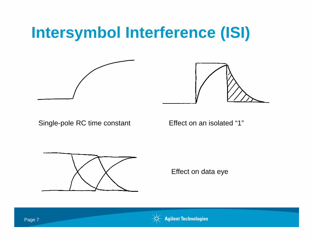
Intersymbol Interference (ISI)
Single-pole RC time constant Effect on an isolated “1”Single-pole RC time constant Effect on an isolated “1”
Effect on data eye
Page 7

Inter-Symbol Interference (ISI)
Threshold
Transmission Line Bandwidth Limitation ProblemA
B
C
1
00
1 1 1 1 1 1 1 1 1 1
0 0 0 0 0 0 0 0 0
TIE Trend Waveform
“A” = 0 preceded by string of 1’s = + error
“B” = 1 preceded by 0 = - error
“C” = 1 preceded by string of 0’s = + error
Page 8

Definition of ISI
Page 9

Data Dependent JitterInteraction of ISI and DCD means
The characterization of a backplane changes with
•DCD
•Data rate
•Data pattern
0 ps
-10 ps
10 ps
20 ps
-20 ps
DDJ
Page 10

Effect of Jitter on the Eye DiagramIdeal Trigger Signal:
Jittered Data:
1 0 1 1 0 1 0 1 1 1 0 0 1 1 0 1
Ideal Data:
1 0 1 1 0 1 0 1 1 1 0 0 1 1 0 1
Jitter in the Eye Diagram:
1 0 1 1 0 1 0 1 1 1 0 0 1 1 0 1
Page 11

Key measure is eye quality
Unequalized 1Gb/s Unequalized 3Gb/s
Cleaning The Rusty Channel
Emphasis, Equalization & Embedding
Unequalized 1Gb/s Unequalized 3Gb/s
Unequalized 8Gb/sUnequalized 5Gb/s
Page 12

How to clean the ‚rusty‘ channel
1111001101
De-emphasis Equalisation
Cleaning The Rusty Channel
Emphasis, Equalization & Embedding Page 13
Agenda1. Introduction
2. Pre-Emphasis
3. Equalization
4. Virtual probing / De-Embedding
Cleaning The Rusty ChannelEmphasis, Equalization & Embedding
4. Virtual probing / De-Embedding
5. Probing Hardware
6. Practical examples
7. Summary
Page 14
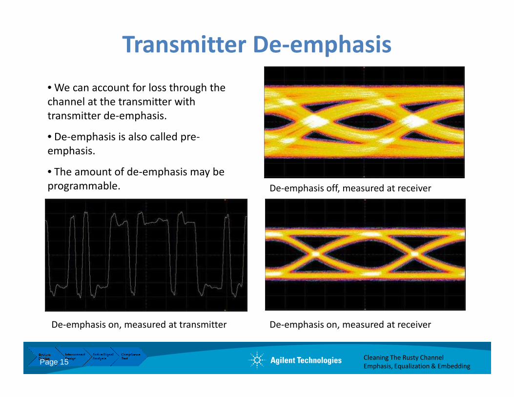
Transmitter De-emphasis
De-emphasis off, measured at receiver
• We can account for loss through the
channel at the transmitter with
transmitter de-emphasis.
• De-emphasis is also called pre-
emphasis.
• The amount of de-emphasis may be
programmable.
Cleaning The Rusty Channel
Emphasis, Equalization & Embedding
De-emphasis on, measured at receiverDe-emphasis on, measured at transmitter
Page 15

Emphasis
Cleaning The Rusty Channel
Emphasis, Equalization & Embedding Page 16
Figure above shows the waveform of a de-emphasized signal. Sometimes this is
called pre-emphasis, as one could see it as boosting the first cycle after a
transition. However, usually the signal’s amplitude is reduced after a delay of one
unit interval (UI), if the data content does not change,so the method is called de-
emphasis.
Loss can be compensated for at the transmitting and the receiving end. At the
transmitter the loss can be compensated either by boosting the higher frequency
content (pre-emphasis) or by decreasing the low frequency content (de-emphasis).
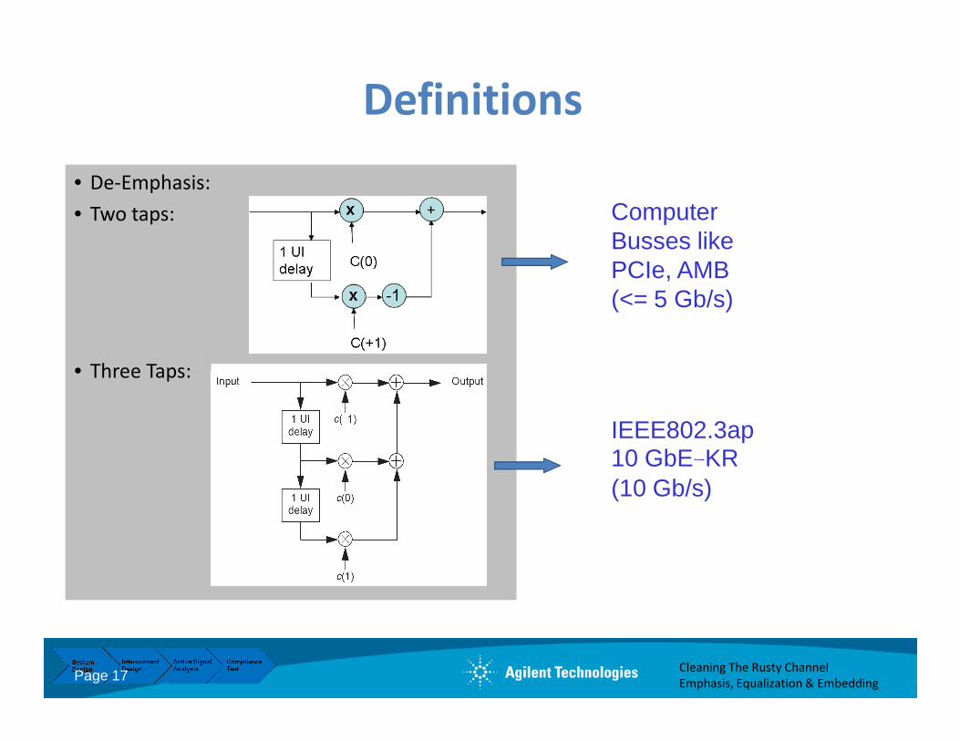
Definitions
• De-Emphasis:
• Two taps:
• Three Taps:
Computer Busses like PCIe, AMB (<= 5 Gb/s)
Cleaning The Rusty Channel
Emphasis, Equalization & Embedding
• Three Taps:
IEEE802.3ap 10 GbE–KR(10 Gb/s)
Page 17
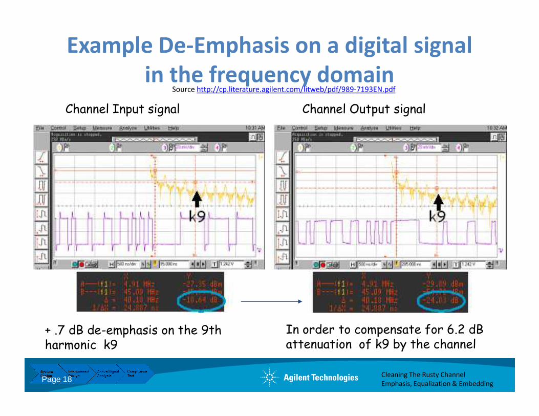
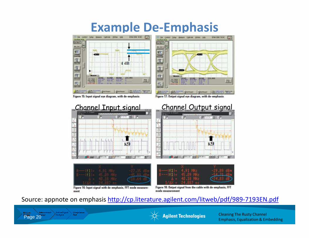
Example De-Emphasis on a digital signal
in the frequency domain
Channel Input signal Channel Output signal
Source http://cp.literature.agilent.com/litweb/pdf/989-7193EN.pdf
Cleaning The Rusty Channel
Emphasis, Equalization & Embedding
In order to compensate for 6.2 dB attenuation of k9 by the channel
+ .7 dB de-emphasis on the 9th harmonic k9
Page 18
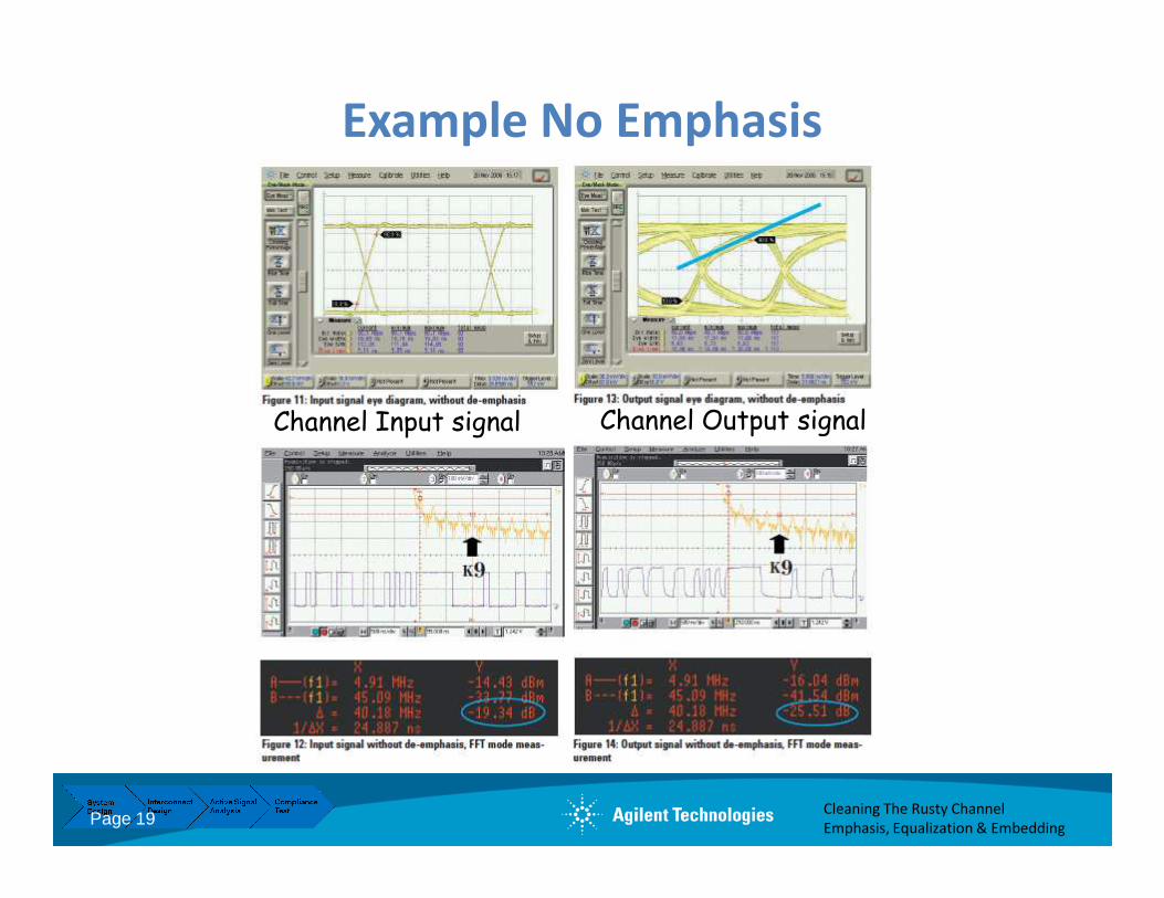
Example No Emphasis
Channel Input signal Channel Output signal
Cleaning The Rusty Channel
Emphasis, Equalization & Embedding Page 19
Example De-Emphasis
Channel Input signal Channel Output signal
Cleaning The Rusty Channel
Emphasis, Equalization & Embedding Page 20
Source: appnote on emphasis http://cp.literature.agilent.com/litweb/pdf/989-7193EN.pdf

De-Emphasis with N4916A (De-Emphasis Signal Converter)
Positive de-emphasisprogramming
Negative de-emphasisprogramming
„start of pulse“
„end of pulse“
Cleaning The Rusty Channel
Emphasis, Equalization & Embedding
Negative de-emphasisprogramming
Page 21
Note:
de-emphasis is sometimes called also pre-emphasis.
Used in standards: PCI Express 1 and 2, SATA 3G b/s, fully buffered DIMM, Hypertransport, CEI 6/11G, 10 Gb Ethernet.
„end of pulse“

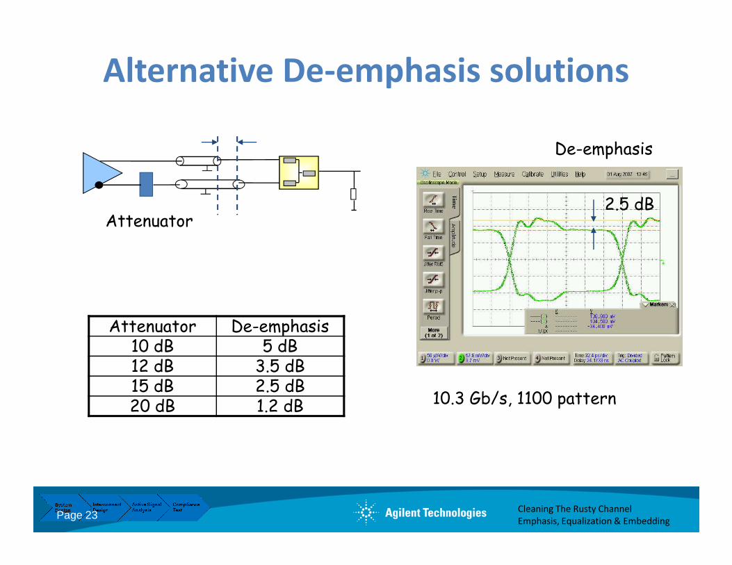
Alternative De-emphasis solutions
• Fixed Delay for differential data
Zl = 50 Ohm
In
1 UI
Power Divider
Cleaning The Rusty Channel
Emphasis, Equalization & Embedding
N_In
Zl = 50 Ohm
Attenuator
Page 22
Alternative De-emphasis solutions
2.5 dBAttenuator
De-emphasis
Cleaning The Rusty Channel
Emphasis, Equalization & Embedding
Attenuator De-emphasis10 dB 5 dB12 dB 3.5 dB15 dB 2.5 dB20 dB 1.2 dB 10.3 Gb/s, 1100 pattern
Page 23

Alternative De-emphasis solutions: 81134A
Use a power divider ( Agilent 11636B) to physically combine channel 1 and channel 2
On channel 1 program the voltage levels to achieve voltage levels in the “middle” of the pre-
and de-emphasis ·
With channel 2 the de-emphasis is realized: Program the levels without any DC offset and
generate the pre- or de-emphasis.
Cleaning The Rusty Channel
Emphasis, Equalization & Embedding Page 24

Example Backplane @ 5 Gb/sin out
no de-emphasis
Cleaning The Rusty Channel
Emphasis, Equalization & Embedding
optimizedde-emphasisWithN4916A
Page 25

Example Motherboard @ 10 Gb/s
no de-emphasis
in (green) & out (yellow)
optimized de-emphasis (three taps)
Cleaning The Rusty Channel
Emphasis, Equalization & Embedding
maximum de-emphasis (two taps)
Page 26

3 taps Emphasis with N4916A J-bert
Cleaning The Rusty Channel
Emphasis, Equalization & Embedding Page 27

Agenda
1. Introduction
2. Eye Masks & TDR with an Network Analyzer
3. Pre-Emphasis
4. Equalization
Cleaning The Rusty ChannelEmphasis, Equalization & Embedding
4. Equalization
5. Virtual probing / De-Embedding
6. Probing Hardware
7. Practical examples (see next page)
8. Summary
Page 28
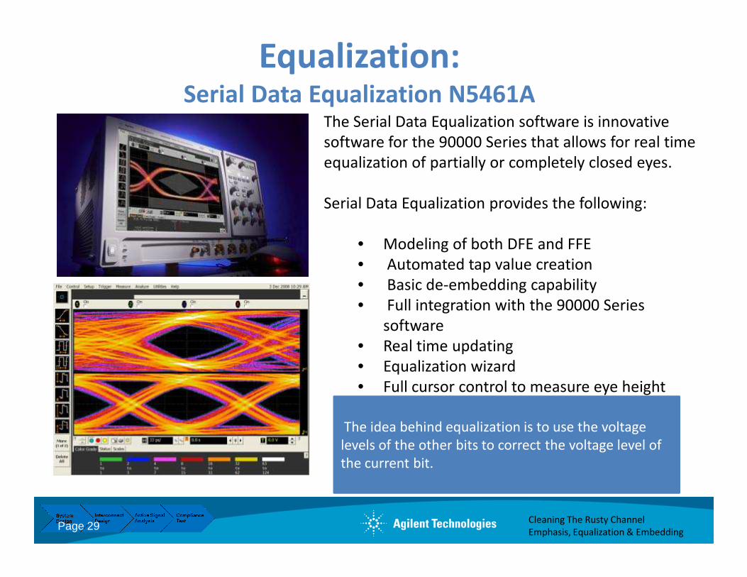
Equalization: Serial Data Equalization N5461A
The Serial Data Equalization software is innovative
software for the 90000 Series that allows for real time
equalization of partially or completely closed eyes.
Serial Data Equalization provides the following:
• Modeling of both DFE and FFE
• Automated tap value creation
• Basic de-embedding capability
Cleaning The Rusty Channel
Emphasis, Equalization & Embedding
• Basic de-embedding capability
• Full integration with the 90000 Series
software
• Real time updating
• Equalization wizard
• Full cursor control to measure eye height
The idea behind equalization is to use the voltage
levels of the other bits to correct the voltage level of
the current bit.
Page 29
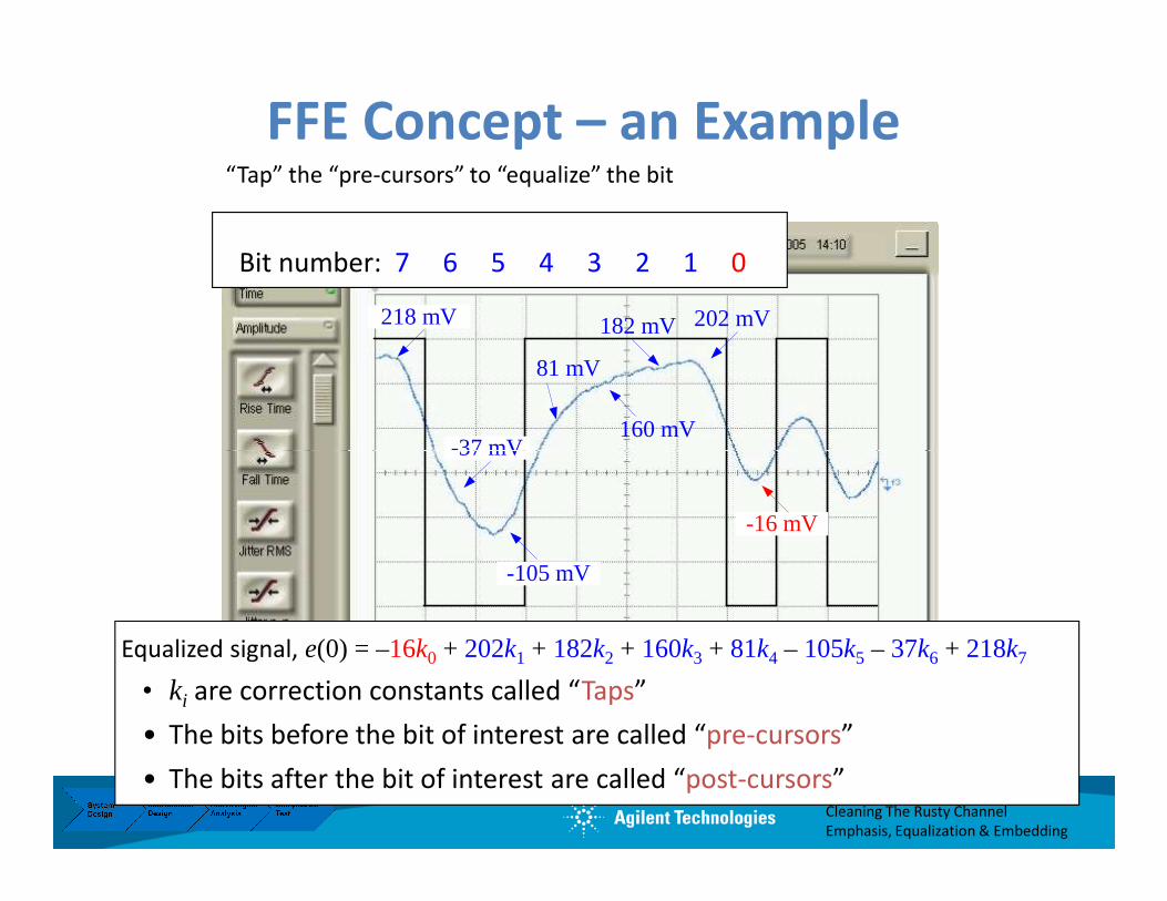
FFE Concept – an Example
218 mV
-37 mV
81 mV
160 mV
182 mV 202 mV
“Tap” the “pre-cursors” to “equalize” the bit
Bit number: 7 6 5 4 3 2 1 0
Cleaning The Rusty Channel
Emphasis, Equalization & Embedding
-37 mV
-105 mV
-16 mV
Equalized signal, e(0) = –16k0 + 202k1 + 182k2 + 160k3 + 81k4 – 105k5 – 37k6 + 218k7
• ki are correction constants called “Taps”
• The bits before the bit of interest are called “pre-cursors”
• The bits after the bit of interest are called “post-cursors”

Feed-Forward Equalization (FFE)
Delay Delay Delayr(n)r(n)r(n)r(n) r(nr(nr(nr(n----1)1)1)1) r(nr(nr(nr(n----2)2)2)2)
r(nr(nr(nr(n----(N(N(N(N----1))1))1))1))
TapTapTapTap0000 TapTapTapTap1111 TapTapTapTapNNNN----1111TapTapTapTap2222
Cleaning The Rusty Channel
Emphasis, Equalization & Embedding
e(n)e(n)e(n)e(n)
∑−
=
−=1
0
N
k
k k))r(n(Tape(n) ∑−
=
−=1
0
)()()(N
k
knrkfnegives or
f(k) f(k) f(k) f(k) = = = = TapsTapsTapsTaps(k)(k)(k)(k) ⊗⊗⊗⊗ LP(bw) LP(bw) LP(bw) LP(bw) where LP is a 4where LP is a 4where LP is a 4where LP is a 4thththth order order order order Bessel.Bessel.Bessel.Bessel.
Tap values are dimensionless; they Tap values are dimensionless; they Tap values are dimensionless; they Tap values are dimensionless; they are a ratio of the voltage the are a ratio of the voltage the are a ratio of the voltage the are a ratio of the voltage the receiver should have seen to what it receiver should have seen to what it receiver should have seen to what it receiver should have seen to what it does see. does see. does see. does see. TapTapTapTap0000 is applied to the is applied to the is applied to the is applied to the current bit.current bit.current bit.current bit.
Decision
Circuit
Page 31

3 tap FFE example from N5461A manual
Note Gustaaf: FFE is like a FIR filter
Cleaning The Rusty Channel
Emphasis, Equalization & Embedding Page 32
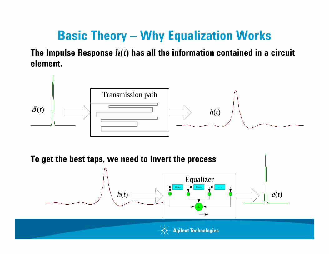
Basic Theory – Why Equalization Works
The Impulse Response h(t) has all the information contained in a circuit
element.
δ (t) h(t)
Transmission path
To get the best taps, we need to invert the process
h(t) e(t)
EqualizerDelay . . .Delay
++++
x x x x

Basic Theory – Why Equalization Works ISI ⇔⇔⇔⇔ Transfer Function ⇔⇔⇔⇔ Ideal Taps
The impulse response is related to the transfer function through a Laplace transform L [h(t)] = G(s) where s is the Laplace parameter, s = jωωωω + ααααThe Transfer Function, G(s), describes how a signal is affected by a network element
S = transmitted signal, R = received signal
)()()( sRsSsG =
S = transmitted signal, R = received signal
• ISI is contained in G(s).
• The ideal equalizer comes from the inverse of the transfer function, G(s)-1.
• Get the signal back as it was transmitted:
(except for random noise . . .)
)()()()()()( 11 sSsRsGsSsGsG == −−

Basic Theory – Why Equalization Works ISI ⇔⇔⇔⇔ Transfer Function ⇔⇔⇔⇔ Ideal Taps
• To get to the time domain take the inverse Laplace transform
• gI(t) ∗ ∗ ∗ ∗ r(t) is the convolution given by
)()()()]()([ 11 tstrtgsRsG I =∗=−−L
∫ −∗=∗ duutrugtrtg II )()()()(
• Or, for a discrete system, by
… which is an LFE with N taps, f(n) ~ gI(n)∑−
=
−=1
0
)()()(N
k
knrkfne
∑=
−=∗N
kII knrkgnrng
1
)()()()(

Basic Theory – Why Equalization Works
Ideal vs actual LFE – MFB
The step from continuous, gI(t), to discrete, f(n) , makes a big difference
• The number of taps went from infinity to about 5 (which is << ∞∞∞∞)
The Matched Filter Bound (MFB) is the maximum possible signal to noise ratio when an equalizer exactly cancels ISI
Let h(i) be the impulse response of the channel, thenLet h(i) be the impulse response of the channel, then
∑ ∑∑−
=
−
=
∞
=
−+−−=1
0
1
00
)()()()()()(N
k
N
ki
knwkfiknsihkfne

The Decision Feedback Equalizer (DFE)
Start with an LFE and . . . fix it!
A perfect equalizer would remove all ISI,
leaving just the signal and the filtered noise
But an LFE:
1. Is discrete – usually one tap per bit, ISI is continuous.
∑−
=
−+=1
0
)()()()(N
k
knwkfnsne
1. Is discrete – usually one tap per bit, ISI is continuous.
2. Is finite – not long enough to completely correct the impulse
response.
3. Only uses information from the current and previous bits.
Introduce another correction based on the best guess of the current
and previous bits – a feedback term – to cancel the rest of the ISI
i.e., use the logic Decision to Feedback to the LFE output for better
Equalization

Decision Feedback Equalization (DFE)
Hardware Receiver
Delay Delay Delays(n)s(n)s(n)s(n) s(ns(ns(ns(n----1)1)1)1) s(ns(ns(ns(n----2)2)2)2)
s(ns(ns(ns(n----N)N)N)N)
TapTapTapTap1111 TapTapTapTapNNNNTapTapTapTap2222
Decision
Circuit
Tap values are dimensionless Tap values are dimensionless Tap values are dimensionless Tap values are dimensionless scalars applied to the +/scalars applied to the +/scalars applied to the +/scalars applied to the +/----
r(n)r(n)r(n)r(n)
b(n) b(n) b(n) b(n) 1011001…1011001…1011001…1011001…
Cleaning The Rusty Channel
Emphasis, Equalization & Embedding
∑=
−−=N
k
k k))s(n(Tapnrnb1
)()(gives
ThresholdThresholdThresholdThreshold
scalars applied to the +/scalars applied to the +/scalars applied to the +/scalars applied to the +/----amplitude voltages. amplitude voltages. amplitude voltages. amplitude voltages.
)(:?)()( AmplitudeAmplitudeThresholdnrns DC −>=
Page 38
• r(n) is the signal at the receiver.
• s(n) is the +/- amplitude as determined by
comparing the incoming signal is the given
Threshold.
• b(n) is the bit sequence coming out of the
receiver.

Decision Feedback Equalization (DFE)
Principle
DFE calculates a correction value that is added to the logical
decision threshold.
This is the threshold above which the waveform is
considered a logical high and below which the waveform is
Cleaning The Rusty Channel
Emphasis, Equalization & Embedding Page 39
considered a logical high and below which the waveform is
considered a logical low.
Therefore, DFE results in the threshold shifting up or down
so new logical decisions can be made on the waveform
based upon this new equalized threshold level.

Decision Feedback Equalization (DFE)
Infiniium Implementation
Delay Delay Delays(n)s(n)s(n)s(n) s(ns(ns(ns(n----1)1)1)1) s(ns(ns(ns(n----2)2)2)2)
s(ns(ns(ns(n----N)N)N)N)
TapTapTapTap1111 TapTapTapTapNNNNTapTapTapTap2222Real Time
Eye
s(n) s(n) s(n) s(n) is the upper target or is the upper target or is the upper target or is the upper target or lower target as determined by lower target as determined by lower target as determined by lower target as determined by clock recovery.clock recovery.clock recovery.clock recovery.
Tap values are dimensionless Tap values are dimensionless Tap values are dimensionless Tap values are dimensionless
r(n)r(n)r(n)r(n)
e(n)e(n)e(n)e(n)
Clock
Recovery
Cleaning The Rusty Channel
Emphasis, Equalization & Embedding
−−= ∑=
N
k
k knsTapnrAne1
)()()()(
∑=
−−=N
k
k k))s(n(Tapnre(n)1
)(gives or
OffsetOffsetOffsetOffset AAAA is the gain. is the gain. is the gain. is the gain. AAAA is computed is computed is computed is computed when Normalize DC Gain is when Normalize DC Gain is when Normalize DC Gain is when Normalize DC Gain is selected.selected.selected.selected.
Tap values are dimensionless Tap values are dimensionless Tap values are dimensionless Tap values are dimensionless scalars applied to the target scalars applied to the target scalars applied to the target scalars applied to the target voltages. voltages. voltages. voltages.
40
)arg(:arg?)()( etLowerTetUpperTThresholdnrns m −>=
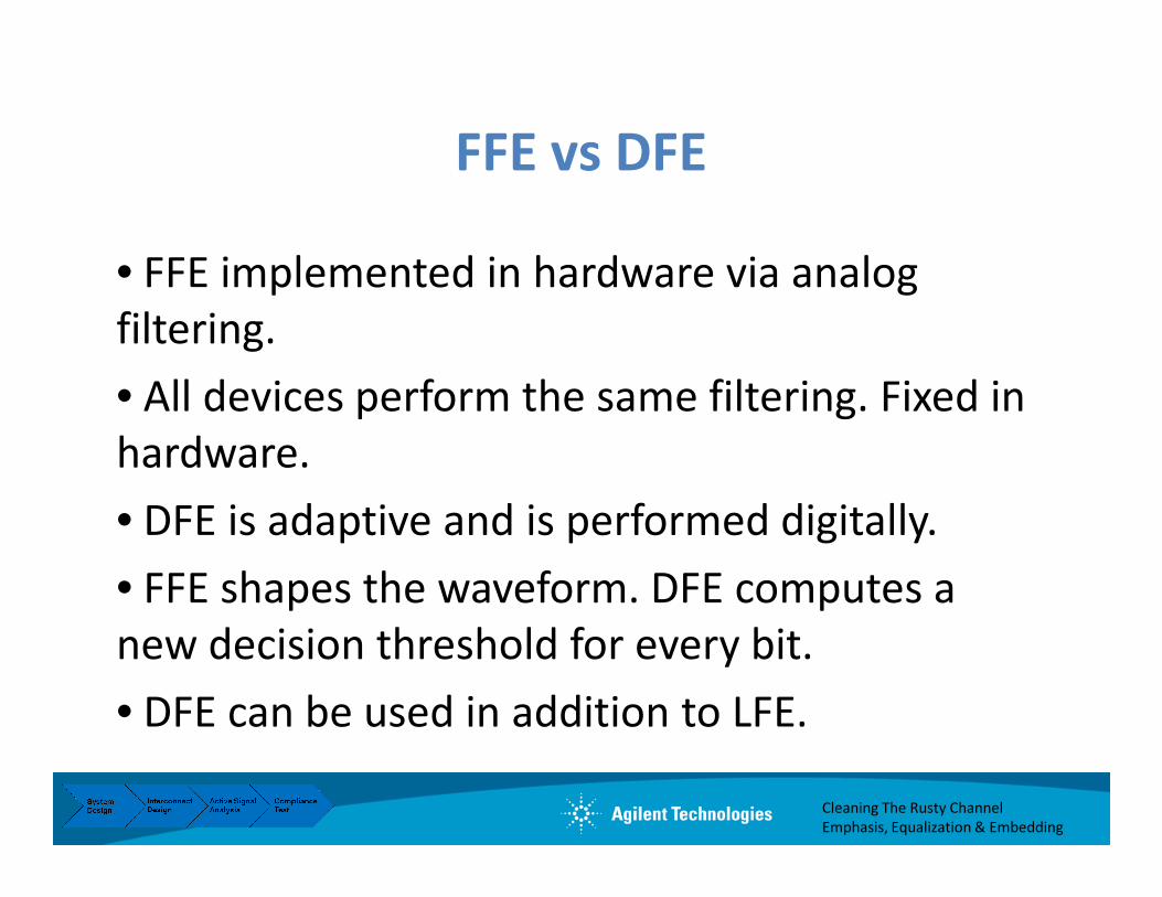
FFE vs DFE
• FFE implemented in hardware via analog
filtering.
• All devices perform the same filtering. Fixed in
hardware.
Cleaning The Rusty Channel
Emphasis, Equalization & Embedding
hardware.
• DFE is adaptive and is performed digitally.
• FFE shapes the waveform. DFE computes a
new decision threshold for every bit.
• DFE can be used in addition to LFE.

Difference Between FFE and DFEDFE=Decision Feedback Equalization
FFE= Feed Forward Equalization Key feature DFE FFE
Flexibility DFE is adaptive and is
performed digitally. The DFE
system learns the tap values
(tap values are dimensionless
correction factors).
FFE implemented in
hardware via analog
filtering. All devices
perform the same
filtering in FFE
Cleaning The Rusty Channel
Emphasis, Equalization & Embedding
correction factors). filtering in FFE
Cost to Implement Expensive Inexpensive
Possible Tap ValuesUnlimited 1
The application of FFE may noise gain.
This makes the oscilloscope industry’s lowest noise floor on the 90000A so important
with equalization and de-embedding.

CTLE example from N5461A manual
Continuous Time Linear
equalization (CTLE) is another
linear equalization method.
Many of today’s standards require
CTLE as part of compliance
testing.
When performing equalization on
your Infiniium oscilloscope, you
Cleaning The Rusty Channel
Emphasis, Equalization & Embedding Page 43
your Infiniium oscilloscope, you
choose whether you want to use
FFE or CTLE (or neither) for your
linear equalization method.
The filter applied to your signal
via CTLE is described by:
DC Gain (Adc), Zero Frequency (Wz), Pole 1 (Wp1), Pole 2 (Wp2)

Serial Data Equalization Provides a Complete
Equalization Wizard and Automated Tap Values
Cleaning The Rusty Channel
Emphasis, Equalization & Embedding
1. Wizard allows for seven real time eye options (including DFE and FFE on a closed eye)
2. Wizard provides full step by step process for clock recovery
3. Wizard provides tap value automation via the FFE and DFE setup menus
4. Wizard makes setting up equalization fast and easy
Page 44

N5461A Equalization Wizard options
1. FFE is applied, but the real time eye is
not displayed. You will see only the
waveform.
2. No equalization applied. This is to
compare an equalized signal versus a non-
equalized signal.
3. FFE is applied only to recover the clock,
but the referenced eye is unequalized. This
is useful forfinding the recovered clock
from a closed eye.
1
2
3
4
Cleaning The Rusty Channel
Emphasis, Equalization & Embedding Page 45
from a closed eye.
4. Standard FFE equalization.
5. Standard DFE equalization for a non
closed eye.
6. Standard DFE equalization for a closed
eye. Note the FFE is used to recover the
clock, but is notdisplayed in the real time
eye.
7. FFE is applied and then DFE is applied to
the real time eye. Both are displayed in the
resulting realtime eye.
4
5
6
7

N5461A Equalization Wizard options
Cleaning The Rusty Channel
Emphasis, Equalization & Embedding Page 46

Equalizer demonstration
• 81134A as ideal source
•“Bad cable” as medium
•90.000 scope as receiver with N5461A
equalizer
Cleaning The Rusty Channel
Emphasis, Equalization & Embedding Page 47
equalizer
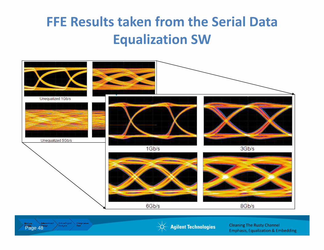
FFE Results taken from the Serial Data
Equalization SW
Cleaning The Rusty Channel
Emphasis, Equalization & Embedding Page 48

DFE Results taken from the Serial Data
Equalization SW
Cleaning The Rusty Channel
Emphasis, Equalization & Embedding Page 49
Agenda
1. Introduction
2. Eye Masks & TDR with an Network Analyzer
3. Pre-Emphasis
4. Equalization
Cleaning The Rusty ChannelEmphasis, Equalization & Embedding
4. Equalization
5. Virtual probing / De-Embedding
6. Probing Hardware
7. Practical examples (see next page)
8. Summary
Page 50

EQ+
-
Connector
TP0 TP1
Channel
Connector
EQ+
-
TP2 TP3 TP4
Txp
Txn Rxn
Rxp
Tx Rx
De-embedding Fixtures or PCB Traces
Signal generated hereExits IC hereExits board here
Combine measurements and transmission line models to view simulated scope measurements at any location in your design
Intuitive GUI speeds setup
51
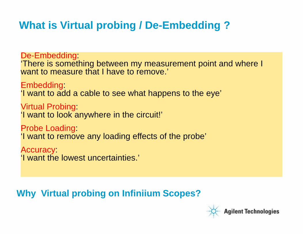
What is Virtual probing / De-Embedding ?
De-Embedding: ‘There is something between my measurement point and where I want to measure that I have to remove.’
Embedding: ‘I want to add a cable to see what happens to the eye’
Virtual Probing: ‘I want to look anywhere in the circuit!’‘I want to look anywhere in the circuit!’
Probe Loading: ‘I want to remove any loading effects of the probe’
Accuracy: ‘I want the lowest uncertainties.’
Why Virtual probing on Infiniium Scopes?
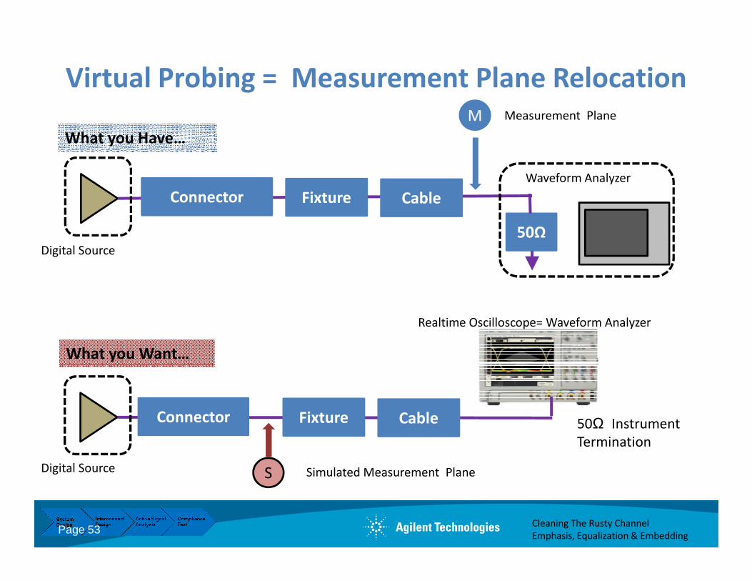
Virtual Probing = Measurement Plane Relocation
50Ω
M
Waveform Analyzer
Connector Fixture Cable
What you Have…
Measurement Plane
Digital Source
Cleaning The Rusty Channel
Emphasis, Equalization & Embedding
50Ω Instrument
Termination
What you Want…
S
Connector Fixture Cable
Realtime Oscilloscope= Waveform Analyzer
Simulated Measurement PlaneDigital Source
Page 53
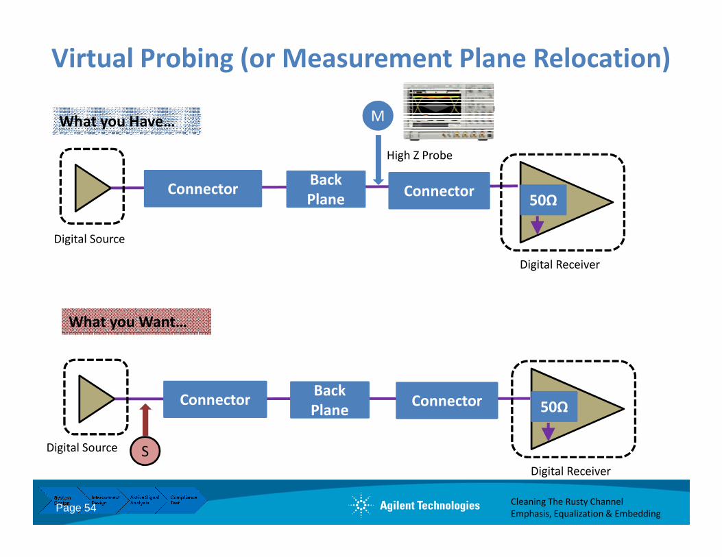
Virtual Probing (or Measurement Plane Relocation)
What you Have… M
ConnectorBack
PlaneConnector
High Z Probe
50Ω
Digital Receiver
Digital Source
Cleaning The Rusty Channel
Emphasis, Equalization & Embedding
What you Want…
S
ConnectorBack
PlaneConnector 50Ω
Digital Receiver
Digital Source
Page 54

Transfer Functions
• A Transfer Function describes the ratio of a voltage wave
entering/exiting one port to a voltage wave exiting/entering
another port.
• An S-Parameter or combination of S-Parameters can be used
as a Transfer Function.
• Transfer Functions are commonly described in the frequency
domain H(s), where s=jw
If you want to see signal at S but can only measure at M, what do you do?
Cleaning The Rusty Channel
Emphasis, Equalization & Embedding
domain H(s), where s=jw
B1 2
50Ω
M
S
A1 2DeviceMeasurement Plane
Simulated
Measurement Plane
Digital Source
Page 55
Transfer Functions, continued
B1 2
50Ω
M
S
A1 2Device Measurement Plane
Simulated
Measurement Plane
VS
M * H (s) = S
Cleaning The Rusty Channel
Emphasis, Equalization & Embedding
M S
M(k) * H(n-k) = S(n)
Acquisition Data Simulated Measurement
Discrete Time Representation
of Transfer Function
Page 56
PHYPHY
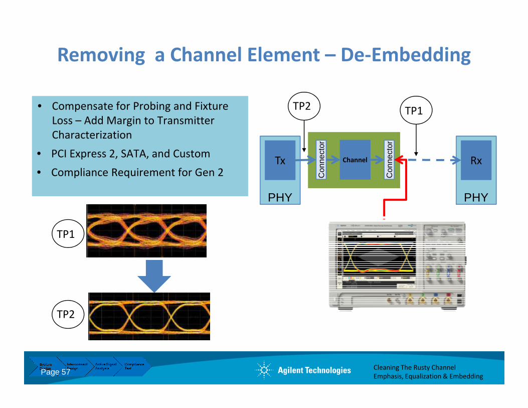
Removing a Channel Element – De-Embedding
Tx Rx
Con
nect
or
Con
nect
or
Channel
• Compensate for Probing and Fixture
Loss – Add Margin to Transmitter
Characterization
• PCI Express 2, SATA, and Custom
• Compliance Requirement for Gen 2
• Compensate for Probing and Fixture
Loss – Add Margin to Transmitter
Characterization
• PCI Express 2, SATA, and Custom
• Compliance Requirement for Gen 2
TP1TP2
Cleaning The Rusty Channel
Emphasis, Equalization & Embedding Page 57
TP1
TP2
PHYPHY
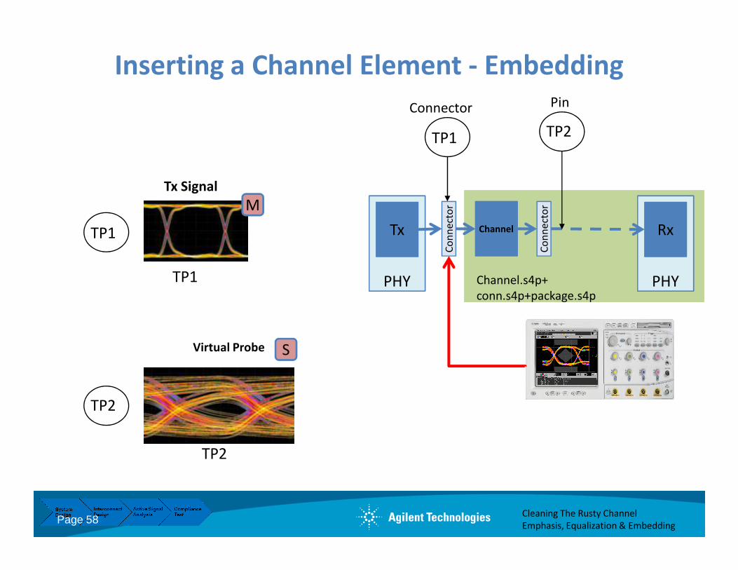
Inserting a Channel Element - Embedding
Tx Rx
Co
nn
ect
or
Co
nn
ect
or
Channel
TP1 TP2
Connector Pin
Channel.s4p+
Tx Signal
TP1
M
TP1
Cleaning The Rusty Channel
Emphasis, Equalization & Embedding
PHYPHY Channel.s4p+
conn.s4p+package.s4p
Virtual Probe
TP2
S
Page 58
TP2

Agilent De-Embedding Representation: InfiniiSim
Example Remove Insertion Loss of 1 Channel Element
Cleaning The Rusty Channel
Emphasis, Equalization & Embedding Page 59

InfiniiSim: Go as Detailed as you need
From 1 block
Cleaning The Rusty Channel
Emphasis, Equalization & Embedding Page 60
To 9 blocks
T= Tx, R = Rx, M = scope, S= Virtual probing point
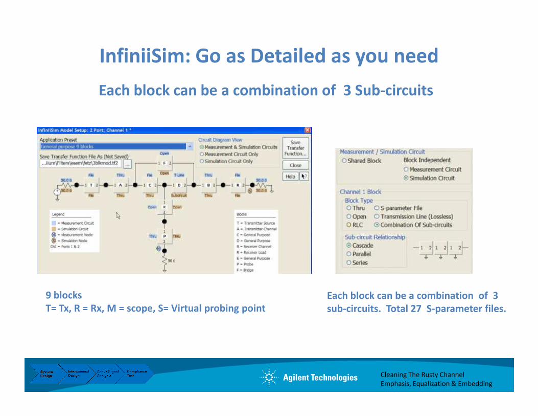
InfiniiSim: Go as Detailed as you need
Each block can be a combination of 3 Sub-circuits
Cleaning The Rusty Channel
Emphasis, Equalization & Embedding
9 blocks
T= Tx, R = Rx, M = scope, S= Virtual probing point
Each block can be a combination of 3
sub-circuits. Total 27 S-parameter files.
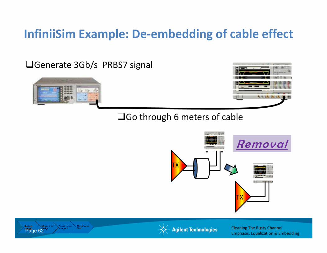
InfiniiSim Example: De-embedding of cable effect
Generate 3Gb/s PRBS7 signal
Go through 6 meters of cable
Cleaning The Rusty Channel
Emphasis, Equalization & Embedding
RemovalRemoval
TX
TX
Page 62

InfiniiSim Example: De-Embedding of 6 meter Cable
We are going to perform a Transformation of a Waveform
ACQUISITION of signal
through 6 meters of cable
Simulated Result of
removing the cable
Cleaning The Rusty Channel
Emphasis, Equalization & Embedding
R(t) ∗ H(t) = S(t)
Transfer Function
Page 63

InfiniiSim Example: De-Embedding DDR2 BGA Probe
Probe_out
DRAM
System
TranTran1
MaxTimeStep=1.0 nsecStopTime=3.0 nsec
TRANSIENT
VtStepSRC1
Rise=1 psecDelay=.1 nsecVhigh=2 VVlow=0 Vt
TermTerm1
Z=75 OhmNum=1 Term
Term2
Z=75 OhmNum=2 Term
Term3
Z=75 OhmNum=3
S2P_EqnS2P1
Z[2]=75Z[1]=29050S[2,2]=0S[2,1]=sqrt(29050/75)S[1,2]=0.01S[1,1]=0
SPOutputspOutput1
Format=MAFileType=touchstoneFileName=
S_ParamSP1
Step=0.01 GHzStop=20 GHzStart=50 Mhz
S-PARAMETERS
RTerm8R=75 OhmR
Term7R=75 OhmR
Term6R=75 Ohm
RTerm4R=75 Ohm
RTerm9R=50 Ohm
W2635_36_RevA1_Model_NoProbe_SUBCKTX1
Vic1_BotVic1_Top
Vic2_Bot
Vic2_Top
Vic1_Probe
Vic2_Probe
Aggr_Top
Aggr_Bot
Aggr_Probe
64
CC1C=.24 pF
RTerm5R=75 Ohm
May 28th, 2009

Probe at BGA
Probe at VIA
De-embed Probe
RT BGA = 390 psRT VIA = 183 ps
RT De-embed = 175 ps
65 May 28th, 2009
InfiniiSim Example: De-Embedding DDR2 BGA Probe

Full De-Embedding versus Insertion Loss Removal
ChannelElement
‘B’
ChannelElement
‘C’
ChannelElement
‘A’
VMeas(t)
TX
F u l l D eF u l l D e -- Emb edd i n gEmb edd i n g
ChannelElement
‘B’
TX
VS.
I n s e r t i o n L o s s R emo v a lI n s e r t i o n L o s s R emo v a l

System Model
A B C
S S S
TX
S21Tx S21RxS21A
S12A
S11A S22A
S21B
S12B
S11B S22B
S21C
S12C
S11C S22C
TFABC = S21A*S21B*S21C
1 – (S22A*S11B + S22B*S11C + S21B*S11C*S12B*S22A )
S21Tx S21Rx
S22Tx = 0 S11Rx = 0
C o r r e c t A n sw e r

A B C
S S S
TX
S21Tx
Comparing the two: Insertion Loss Removal I n s e r t i o n L o s s R emo v a l U s e s “ e a s y s c o p e ma t h ” : S21B
-1
S21A
S12A
S11A S22A
S21B
S12B
S11B S22B
S21C
S12C
S11C S22C
TFABC = S21A*S21B*S21C
1 – (S22A*S11B + S22B*S11C + S21B*S11C*S12B*S22A )
G i v e n A n sw e r
S21Tx
S22Tx = 0
I n t e r a c t i o n A r t i f a c t s A r e S t i l l T h e r e ! ! !
S21B-1
“Easy” Scope ‘Math’
S21B-1
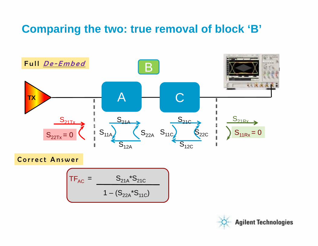
Comparing the two: true removal of block ‘B’
A
B
C
S21A S21C
TX
F u l l DeDe -- Emb edEmb ed
S21Tx S21RxS21A
S12A
S11A S22A
S21C
S12C
S11C S22C
TFAC
1 – (S22A*S11C)
= S21A*S21C
C o r r e c t A n sw e r
S21Tx
S22Tx = 0 S11Rx = 0

A B C
S S S
TX
S21Tx
F u l l DeDe -- Emb edEmb ed
Comparing the two: Full De-embed
As measured
Complex Function
F u l l D e - Emb ed u s e s “ c omp l e x s c o p e ma t h ” t h a t r emo v e s a l s o i n t e r a c t i o n a r t i f a c t s ( i n t h i s c a s e b e t w e e n A - B a n d B - C a n d A - B - C ) :
S21A
S12A
S11A S22A
S21B
S12B
S11B S22B
S21C
S12C
S11C S22C
S21Tx
S22Tx = 0 Scope ‘Math’
= S21A*S21B*S21C
[1 – (S22A*S11B + S22B*S11C + S21B*S11C*S12B*S22A )]
[1 – (S22A*S11B + S22B*S11C + S21B*S11C*S12B*S22A )] S21B-1
[1 – (S22A*S11C)]
TFAC
I n t e r a c t i o n A r t i f a c t s A r e R emo v e d ! ! !

DEMO InfiniiSim Virtual Probing
Page 71
Test –Fixture to De-Embed

DEMO JIM&
INFINIISIM81134A/90.000 Setup at Amstelveen Office
Page 72
Infiniisim OFF Infiniisim ON

Agenda1. Introduction
2. Eye Masks & TDR with an Network Analyzer
3. Pre-Emphasis
4. Equalization4. Equalization
5. Virtual probing / De-Embedding
6. Probing Hardware
7. Practical examples
8. Summary
Page 73

How to inject data from PG in embedded design?
Differential traces
Cleaning The Rusty Channel
Emphasis, Equalization & Embedding
Agilent TDR Probe N1021B (100Ohm, 18GHz) mounted in 3D Probe
Positioner N2787A could be used for pattern injection up to 18GHz.
EZ-Probe Positioner from Cascade Microtech, here
shown with 6GHz passive TDR probe N1020A and
Calibration Substrate N1020A-K05. For more
information, see product overview 5968-4811EN.
Wheel for pitch adjustment
Page 74

Differential Connectivity Kit
E2669A Differential Connectivity Kit
Differential Browser
• 6 GHz Bandwidth
• Input R: 50KΩ• Input C: .33 pF
• Variable tip spacing, replaceable tips
• Dual tip Z-axis compliance
Ergonomic browser sleeve
comes standard!
Cleaning The Rusty Channel
Emphasis, Equalization & Embedding
• Dual tip Z-axis compliance
Differential Solder-In
• 7 GHz Bandwidth
• Input R: 50KΩ• Input C: 0.30 pF
• 8 mil tip leads are flexible
Differential Socketed
• 7 GHz Bandwidth
• Input R: 50KΩ• Input C: 0.38 pF
• 100 mil socket spacing, accepts standard
20-mil round resistor leads
comes standard!
Page 75

ZIF Probe HeadsEconomical replaceable solder-in tips
N5451A Long-wire ZIF – extra span
>10 GHz (with 7mm wire) at zero
deg span
> 5GHz (with 11mm wire) at zero
deg span
N5425A ZIF head + N5426A ZIF tips (qty 10)
• Full bandwidth (13 GHz)
Cleaning The Rusty Channel
Emphasis, Equalization & Embedding
Key applications: DDR memory system,
server and storage, embedded
applications
Page 76

6GHz single end 6GHz single end soldersolder--in probe in probe headhead
1212--13GHz differential13GHz differentialbrowser probe headbrowser probe head
6GHz differential6GHz differential1212--13GHz 13GHz
12GHz differential12GHz differentialsoldersolder--in probe headin probe head
InfiniiMax extreme InfiniiMax extreme temp extension cable temp extension cable ((--55 ~ 150 C)55 ~ 150 C)
Probing Solutions for High Speed Realtime Scopes
Cleaning The Rusty Channel
Emphasis, Equalization & Embedding
1212--13GHz SMA 13GHz SMA
probe headprobe head8GHz SMA probe head8GHz SMA probe head
12GHz Socket 12GHz Socket
probe headprobe head
6GHz differential6GHz differentialbrowser probe headbrowser probe head
5GHz single end5GHz single endbrowser probe headbrowser probe head
1212--13GHz 13GHz differentialdifferentialsoldersolder--in probe in probe headhead
1212--13GHz 13GHz differentialdifferentialZIF solderZIF solder--in probe in probe head & ZIF Tip & head & ZIF Tip & Long Wire ZIF Tip Long Wire ZIF Tip (4~9GHz)(4~9GHz)
Page 77

ZIF Probe Head (N5439A)
28 GHz
Probe Pod & Amplifier
Full Bandwidth
ZIF Tips (28 GHz)
2.92/3.5 mm Probe Head
(N5444A) – 28 GHz
Integrated de-
embedding
with
customized s-
parameter
loaded in the
amp
True Analog Bandwidth that Delivers…
Full 30 GHz Probing System
Browser
(N5445A) 30
GHz
Cleaning The Rusty Channel
Emphasis, Equalization & Embedding
Solder-in (N5441A)
Probe 16 GHz
PV/Deskew Fixture
(N5443A)
High Impedance
(N5449A)
Adaptor 500MHz
Sampling Scope Adaptor
(N5477A)
Full Bandwidth
IniniiMax I and II
Adaptor (N5442A)
amp
Fully
upgradeable
hardware
Page 78

Introducing the Infiniium 90000 X-Series Oscillosco pesEngineered for 32 GHz true analog bandwidth that del ivers
The industry’s highest measurement accuracy
Full 30 GHz probing system
The most comprehensive software specific application software software
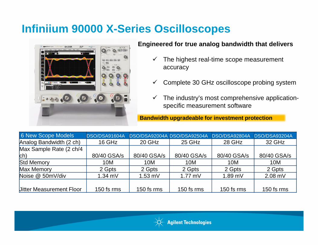
Infiniium 90000 X-Series OscilloscopesEngineered for true analog bandwidth that delivers
The highest real-time scope measurement accuracy
Complete 30 GHz oscilloscope probing system
The industry’s most comprehensive application-specific measurement software
Bandwidth upgradeable for investment protection
6 New Scope Models DSO/DSA91604A DSO/DSA92004A DSO/DSA92504A DSO/DSA92804A DSO/DSA93204AAnalog Bandwidth (2 ch) 16 GHz 20 GHz 25 GHz 28 GHz 32 GHzMax Sample Rate (2 ch/4 ch) 80/40 GSA/s 80/40 GSA/s 80/40 GSA/s 80/40 GSA/s 80/40 GSA/sStd Memory 10M 10M 10M 10M 10MMax Memory 2 Gpts 2 Gpts 2 Gpts 2 Gpts 2 GptsNoise @ 50mV/div 1.34 mV 1.53 mV 1.77 mV 1.89 mV 2.08 mV
Jitter Measurement Floor 150 fs rms 150 fs rms 150 fs rms 150 fs rms 150 fs rms

Agenda1. Introduction
2. Eye Masks & TDR with an Network Analyzer
3. Pre-Emphasis
4. Equalization4. Equalization
5. Virtual probing / De-Embedding
6. Probing Hardware
7. Practical examples
8. Summary
Page 81
Agenda7. Practical Examples
1. High-Speed Characterization (effect of 4.5 GHz Notch in test fixture)
2. BGA probe setup in infiniisim Virtual Probe
3. Tuned, measurement enhanced, IBIS parameters for DDR DDR
4. Creating S2P (touchstone) files from Gerber files
5. Basic Steps for Optimizing a Serial Link
6. Serial Data Analysis Solutions: 8b10b Trigger, Decode, Search and Listing Feature
7. Small peek inside the 90.000 X 32 GHz scope
Page 82

Practical example1
High-Speed IC Characterization
1. Fixture Characterization – obtain your model
2. Simulate waveform using the model
3. Verify model and waveform with an actual measurement
4. Apply the model and De-Embed Fixture
- measure at connectors & simulate signal at balls of IC
Cleaning The Rusty Channel
Emphasis, Equalization & Embedding Page 83
- measure at connectors & simulate signal at balls of IC

Characterizing High-Speed Integrated Circuits (IC)
Precision Characterization
What parameters get measured? Full characterize includes measuring amplitude, rise/fall times, jitter (all types), etc. under various operating conditions.
IC - Top IC - Bottom
Device: ASIC / FPGA / SERDES / Other High-Speed IC
84
(all types), etc. under various operating conditions.
Who? Where? Performed by engineers and technicians in Performance Verification (PV) and Characterization labs
How are they measured?Accuracy and precision is critical, so engineers often use a sampling scope due to:
• High analog bandwidth (18GHz->90GHz)• Low noise (<300uV)• Ultra-low jitter (RJ<60fs)

Custom FixturesAccurate characterization often requires custom fixt ures.
• Probing introduces measurement challenges• Bring signals out to connectors• Good fixture layout minimizes signal degradation
DUTTX Output at the
Test FixtureMeasure actual signal here using cables between fixture and scope (connectorized)
A B
85
pads/balls of the IC
• Problem: Fixture will degrade signal and may not represent e nd-user’s implementation
• Solution: Remove fixture effects of the transmission line fro m pt A to pt B (commonly referred to as de-embedding ). Allows us to predict the TX performance at the balls/pins of the IC, and/or predict performance using a differen t layout/material

Step 1: Fixture Characterization – obtain your mode l Generate an S-parameter model
a. Simulation o Use design software such as Agilent ADS, PLTS
b. Measure o Use VNA (ENA/PNA) or TDRo Do-It-Yourself or consult with an expert
such as GigaTest Labs
Characterize raw (unpopulated) board – plan ahead!• Add test coupons to fixture (e.g. Connector – pad, pad - Connector)• Layout pads with adjacent grounds for probing e.g. GSSG, GSGS, GSGGSG• Full S-Parameters - need differential probe that includes ground contacts
A B
86
Handheld 18GHz Differential TDR Probe - for fully balanced differential signals(no ground contact)
G S G G S G
Differential Probe - usually used with positioner- select specific footprint,pitch, may be adjustable
ConnectorIC Pad
Goal: Accurately characterize the signal path from pad to connector.Generate a .s2p or .s4p Touchstone file.
AA
BB
N1021B

Step 2-3 Use your model to Simulate…then Verify
2. Simulate waveform using model (input –> apply S-parameter model -> output)
• simulate expected DUT TX signal (e.g. 10Gb/s, PRBS7, Rise/Fall Time = 25ps)
SW Simulated Input Signal
SW Simulated Output Signal
Embed Function
Simulated point A Simulated point B
87
3. Verify model and waveform with an actual measurement (inject signal from PG –> actual DUT -> measure O/P)
• generate expected DUT TX signal using BERT, inject via probe, measure on scope
Input Signal from PG Measured Output Signal
Probe DUT(raw board)
Simulated point B
Point A Measured point B
GoodCorrelation

Step 4 - Fixture Removal (de-embedding)
4. De-Embed Fixture- measure at connectors (B), simulate signal at balls of IC (A)
Pink = de -embedded signalYellow = measured signal
De-EmbeddedOutput Signal
Signal from DUT
88
Pink = de -embedded signalYellow = measured signal (Actual DUT + Fixture + Cables)
Benefits:• Improved Margins• More accurate representation of TXperformance (at point ‘A’)
• Simulate signal using different fixturewithout building it (cascade functions)• Gain valuable insightNote – could also remove cable effects too
AB
Measure at Point B Simulated Signal at Point A

Case Study – design your fixtures carefully!
DUT - fixtureSMA-pads
Characterize fixture with Agilent TDR and probe
S-Parameter has notch at 4.5GHz
Eye DiagramPurple – raw signal (reflection)Green – de-embedded signal (noise)
TDR into open (Step Response) has a very long settling time (triple transit)
Step 1
1a
1b
Steps 2, 3, 4a
Hi Z
Nio coupling
A B
probe-> Generate .s4p
notch at 4.5GHzGreen – de-embedded signal (noise)
Summary large notch in S-Parameter due to large reflection in the fixture (be wary of triple-transit !!) the ‘inverse’ function (de-embed) amplifies a lot of noise in the notch region => causes ringing must setup de-embed function to filter out notch at 4.5MHz. if left “as is”, max data rate for fixture ~1Gb/s. analyzing S-parameters can help predict effectiveness of de-embedding (look for excessive loss)
Step 4b5
89
SI design flaws cannot be hidden by De-emphasis, Equalization or de-embedding/virtual probing!!!!!

Agenda7. Practical Examples
1. High-Speed Characterization (effect of 4.5 GHz Notch in test fixture)
2. BGA probe setup in infiniisim Virtual Probe
3. Tuned, measurement enhanced, IBIS parameters for DDR DDR
4. Creating S2P (touchstone) files from Gerber files
5. Basic Steps for Optimizing a Serial Link
6. Serial Data Analysis Solutions: 8b10b Trigger, Decode, Search and Listing Feature
7. Small peek inside the 90.000 X 32 GHz scope
Page 90

BGA BGA BGA BGA ProbeProbeProbeProbe PortPortPortPortMonitoring Pad = 1Monitoring Pad = 1Monitoring Pad = 1Monitoring Pad = 1Memory side =2Memory side =2Memory side =2Memory side =2 Board side = 3Board side = 3Board side = 3Board side = 3 internal branching point = 4 internal branching point = 4 internal branching point = 4 internal branching point = 4
2222
DRAMDRAMDRAMDRAM
BGA Probe BGA Probe BGA Probe BGA Probe
1111
33334444Controller Controller Controller Controller
BGABGABGABGA ProbeProbeProbeProbe
33334444Controller Controller Controller Controller
July 21, 2010

InfiniisimInfiniisimInfiniisimInfiniisim SettingsSettingsSettingsSettings
Rx
Controller
Tx
DRAM
Tx, Rx Impedance Package S-parameters, RLC
ChannelS-parameters
Infiniimax head
S-parameters
BGA Probe S-parameters
July 21, 2010

DRAMDRAMDRAMDRAM
BGA Probe BGA Probe BGA Probe BGA Probe Controller Controller Controller Controller
Observation point shift with Observation point shift with Observation point shift with Observation point shift with InfiniisimInfiniisimInfiniisimInfiniisim
Meas Meas
July 21, 2010
We want to reproduce from and InfiniisimMeasMeas

DRAMDRAMDRAMDRAM
BGA Probe BGA Probe BGA Probe BGA Probe Controller Controller Controller Controller
Meas Meas
Infiniisim
Channel S-parameters
Observation point shift with Observation point shift with Observation point shift with Observation point shift with InfiniisimInfiniisimInfiniisimInfiniisim
Infiniisim
We have only applied the channel S-parameters.
The delay is good, but the reflection and amplitude aren’t reproduced.
That means that it isn’t enough with the channel S-parameters only.
July 21, 2010

DRAMDRAMDRAMDRAM
BGA Probe BGA Probe BGA Probe BGA Probe Controller Controller Controller Controller
Meas Meas
Channel S-parameters
Observation point shift with Observation point shift with Observation point shift with Observation point shift with InfiniisimInfiniisimInfiniisimInfiniisim
Infiniisim
Package S-parameters
and Chip Die capacitance
The delay and the first edge are perfectly reproduced.
But the ripples on the plateau are wrong.
That means that the Infiniisim settings are still wrong or something is lacking.
That is you have to re-examine your simulation. => Let’s go to Example 3
July 21, 2010

Agenda 7. Practical Examples
1. High-Speed Characterization (effect of 4.5 GHz Notch in test fixture)
2. BGA probe setup in infiniisim Virtual Probe
3. Tuned, measurement enhanced, IBIS parameters for DDR
Cleaning The Rusty ChannelEmphasis, Equalization & Embedding
DDR
4. Creating S2P (touchstone) files from Gerber files
5. Basic Steps for Optimizing a Serial Link
6. Serial Data Analysis Solutions: 8b10b Trigger, Decode, Search and Listing Feature
7. Small peek inside the 90.000 X 32 GHz scope
Page 96

Practical example3
Simulation and Measurement Cooperation“connected solutions”
Cleaning The Rusty Channel
Emphasis, Equalization & Embedding Page 97

Simulation and Measurement Cooperation“connected solutions”
Oscilloscope
New Function:InfiniisimSimulation on the scope
Simulator (ADS)Simulation using measured waveform and S-parameters
Network Analyzer
New function:ENA-TDRSimulation on VNA
Agilent is the only one vendor delivering both simulation and measurement !

Simul and Meas, PCB board Straight Line
Straight line (test coupon).We have designed it to be Z=50 Ohm.
0.0
0.1
0.2
0.3
0.4
0.5
-0.1
0.6
Den
sity
2 4 6 8 10 12 14 16 180 20
-60
-50
-40
-30
-20
-10
-70
0
-6
-4
-2
-8
0
freq, GHz
dB(S
(1,1
))
dB(S
(2,1))
100 200 300 400 500 6000 700
time, psec
Simulated eye pattern and S-parameters at the design phase

100 200 300 400 500 6000 700
0.0
0.1
0.2
0.3
0.4
0.5
-0 .1
0.6
time , psec
Den
sity
Simulated Eye at the design phase
Measured Eye
Sim and Meas, PCB board Straight Line
Simulated S-parameters at the design phase
Measured Eye
Measured S-parameters

2 4 6 8 10 12 14 16 180 20
-30
-25
-20
-15
-10
-5
-35
0
-15
-10
-5
-20
0
freq, GHz
dB(S
(1,1
))
dB(S
(1,2))
dB(T
DR
_Tun
ing_
wS
MA
..S(1
,1)) dB
(TD
R_T
uning_wS
MA
..S(1,2))
Sim and Meas, PCB board Straight Line
Tune PCB board parameters so that the simulated and measuredS-parameters, TDR and TDT come very close.
er = 4.2
h= 360um
tanδ = 0.015
er = 4.5
h= 325um
tanδ = 0.023
Tuning Result

100 200 300 400 500 6000 700
0.0
0.1
0.2
0.3
0.4
0.5
-0.1
0.6
time, psec
Den
sity
Simulation before tuning
Sim and Meas, PCB board Straight Line
Simulation after tuning
Measured Eye

More complex channel
Simulation before tuning
Sim and Meas, PCB board Complex Channel
Use the same tuning as the test coupon(tuning parameters 2 slides back )
Simulation after tuning
Measured Eye

Sim and Meas, On Actual Device
Vasic
V_DCSRC7Vdc=Vsrc
IBIS_IIBIS1
UsePkg=yesDataTypeSelector=TypSetAllData=yesModelName="iobuf"PinName="C2"ComponentName="EDE1116AEBG03"IbisFile="C:\Consulting\AICA\TimeDomain_move_obs_point_meas_prj\data\aica-yamaha\ede1116aebg03.ibs"
DigO
I n PC
G C
S2PSNP4File="meas_DQ9_P1ASIC_P2DRAM.ds"
21
R e f
S2PSNP2File="PCB_GP2_Afixed_RBDQ9.ds"
21
R e f
CC5C=1.5 pF
S2PSNP1File="BGA_probe_model.ds"
2
1
Re f
VtBitSeqSRC9
BitSeq="111001000100011101111111111101100110000000001000100010001000000100"Delay=0 nsecFall=0 nsecRise=0 nsecRate=fClockVhigh=1Vlow=0 V
t
VARVAR1
Vsrc=1.75fClock=667MHz
Eqn
Var
IB IS_IOIBIS2
UsePkg=yesDataTypeSelector=TypSetAllData=yesModelName="dq_half_hiz_y0"PinName="M1"ComponentName="Buff1"IbisFile="C:\Consulting\AICA\TimeDomain_move_obs_point_meas_prj\data\aica-yamaha\ygv635-ibs-v118.ibs"
DigO
I O
PD
PU
E
TPC
G C
V_DC
SRC2Vdc=Vsrc
V_DCSRC8Vdc=1V
TranTran1
MaxTimeStep=100nsec/4000StopTime=100 nsec
TRANSIENT
ControllerDRAM
Channel model
BGA Probe
Rx @Controller (READ)- simulation- measurement
Rx @DRAM (WRITE)- simulation- measurement
Is the channel model right ?
Are the devices IBIS model right ?(Same thing for HSPICE model)

Sim and Meas, Device
Measuring channelS-parameters
IBIS model from memory vendor
Package CDie C
ODT
Package, bonding wire
The package C seems to be 2.05pF from the sim model,
Measuring active deviceS-parameters
Tuned IBIS with measured result
The package C seems to be 2.05pF from the sim model,but is it true ?
The package C should be 2.76pF tomake consistent with the measured result.

WRITE- simulation- measurement
Sim and Meas, Device: now with tuned, measurement enhanced, IBIS parameter
READ- simulation- measurement

Simulation on scope
Vasic
V_DCSRC7Vdc=Vsrc
IBIS_IIBIS1
UsePkg=yesDataTypeSelector=TypSetAllData=yesModelName="iobuf"PinName="C2"ComponentName="EDE1116AEBG03"IbisFile="C:\Consulting\A ICA\TimeDomain_move_obs_point_meas_prj\data\aica-yamaha\ede1116aebg03.ibs"
DigO
InPC
GC
S2PSNP4File="meas_DQ9_P1ASIC_P2DRAM.ds"
21
R e f
S2PSNP2File="PCB_GP2_Afixed_RBDQ9.ds"
21
R e f
CC5C=1.5 pF
S2PSNP1File="BGA_probe_model.ds"
2
1
R e f
VtBitSeqSRC9
BitSeq="111001000100011101111111111101100110000000001000100010001000000100"Delay=0 nsecFall=0 nsecRise=0 nsecRate=fClockVhigh=1Vlow=0 V
t
VARVAR1
Vsrc=1.75fClock=667MHz
Eqn
Var
IBIS_IOIBIS2
UsePkg=yesDataTypeSelector=TypSetAllData=yesModelName="dq_half_hiz_y0"P inName="M1"ComponentName="Buff1"IbisFile="C:\Consulting\A ICA \TimeDomain_move_obs_point_meas_prj\data\aica-yamaha\ygv635-ibs-v118.ibs"
DigO
I O
PD
PU
E
TPC
GC
V_DC
SRC2Vdc=Vsrc
V_DCSRC8Vdc=1V
TranTran1
MaxTimeStep=100nsec/4000StopTime=100 nsec
TRANSIENT
Measured waveform at the probing point
Simulated waveform at the DRAMSimulated waveform at the controller

Agenda 7. Practical Examples
1. High-Speed Characterization (effect of 4.5 GHz Notch in test fixture)
2. BGA probe setup in infiniisim Virtual Probe
3. Tuned, measurement enhanced, IBIS parameters for DDR
Cleaning The Rusty ChannelEmphasis, Equalization & Embedding
DDR
4. Creating S2P (touchstone) files from Gerber files
5. Basic Steps for Optimizing a Serial Link
6. Serial Data Analysis Solutions: 8b10b Trigger, Decode, Search and Listing Feature
7. Small peek inside the 90.000 X 32 GHz scope
Page 108

Practical example 4:Creating S2P files from Gerber files
1. Import Layout from mechanical CAD software into Genesys or ADS
2. Inspect layer stack and ensure material propertie s are correct
3. Insert EM Ports and Add Momentum Planar EM simulation controller
Page 109
simulation controller4. Run EM simulation and Graph Results5. Export Touchstone file to use in de-embedding net work
in Scope

Agilent Genesys : Cost Efficient, High Performance R F/MW Board Design Software
RF System Architecture
Circuit
Genesys Core Design Environment
Month ##, 200X
Circuit Syntheses Planar 3D EM Simulation
Frequency-domain Nonlinear
Time-domain
Nonlinear Frequency PlanningAntenna Far Field
Linear Sim& Data Display

GENESYS: An Advanced User Interface
A modern, integrated Windows environment
Easy-to-use - “Hard to forget”
Layouts Equations
TuneWindow
VendorModels
Page 111
Schematics
WorkspaceTree
Graphs& Tables
Window Models

STEP 1: Import Layout from mechanical CAD software into Genesys
Supported File Formats for import:
- DXF DWG- GDS II- Gerber

STEP 2: Inspect layer stack and ensure material properties are correct
Supported File Formats for import:
- DXF DWG- GDS II- Gerber

STEP 3: Insert EM Ports and Add Momentum Planar EM simulation controller

STEP 4: Run EM simulation and Graph Results
- - Layout with Momentum Mesh overlay
- Layout 3D View
-Graph of S-parameters
Very simple to setup for accurate results. All simulation options left to default (automatic)

STEP 5: Export Touchstone file to use in de-embedding network in Scope

Agenda 7. Practical Examples
1. High-Speed Characterization (effect of 4.5 GHz Notch in test fixture)
2. BGA probe setup in infiniisim Virtual Probe
3. Tuned, measurement enhanced, IBIS parameters for DDR
Cleaning The Rusty ChannelEmphasis, Equalization & Embedding
DDR
4. Creating S2P (touchstone) files from Gerber files
5. Basic Steps for Optimizing a Serial Link
6. Serial Data Analysis Solutions: 8b10b Trigger, Decode, Search and Listing Feature
7. Small peek inside the 90.000 X 32 GHz scope
Page 117

Practical example 5:Basic Steps for Optimizing a Serial Link
Page 118

Optimizing a Serial Link
PC BoardDSA9000 series & N5461A Equalization Analysis allows to analyze and optimize the signal integrity
Xilinx:
Multi-Gigabit Transceivers (MGTs)
+ IBERT Test Core
• IBERT core provides stimulus, • Tx & Rx setting control, and • BER measurement capability
Agilent:
Measurement instruments for analysis and optimization of signal integrity of Rocket IO signals
FPGA
IBERTIBERTIBERTIBERT
FPGA
PC Board
IBERTIBERTIBERTIBERTInsert core with
FPGA design SW
N4903B BERT and N4916B De-Emphasized Signal Converter allows to generate any pre-emphasis signal.
allows to analyze and optimize the signal integrity including automated tap optimizer for opening the eye. Graphical margin analysis via eye diagram measurements including mask templates allows to control optimization process.
Page 119

Optimizing Rocket IO Signal IntegrityBasic Steps for Optimizing a Serial Link:
1. Specify MGT configuration using Xilinx ISE tools, per your design’s characteristics.
2. Specify IBERT core parameters using Xilinx ChipScope Pro Core Generator consistent with #1 above; create IBERT core.
3. Load IBERT core and generate serial data .
4. Replace IBERT Tx by SerialBERT + De-Emphasized Sig nal Converter and optimize pre-emphasis controlled by BER
measurement in IBERT Rx or JBERT N4903B. Alternatively, the optimal pre-emphasis setting could be controlled by using the eye measurement in IBERT Rx or JBERT N4903B. Alternatively, the optimal pre-emphasis setting could be controlled by using the eye
opening measurement in the Realtime Scope 90000 series. The results of the optimization taps for Pre-emphasis could directly be
used in the Multi-Gigabit Transceivers (MGT) of Tx.
5. Replace IBERT Rx by Scope and determine the optim al tap values for equalizer in the Rx using automated tap finder routine in
the N5461A Equalization Software. The result of optimal equalization could be controlled by eye opening measurement in the
Realtime Scope 90000 series at Rx. The optimal settings for equalization taps could directly be used in the MGT of the Rx.
Page 120

Practical example 6Serial Data Analysis Solutions
1. Mask Unfold Feature2.8b10b Trigger, Decode Feature, 3.Search and Listing Feature
Page 121

The weakness of the mask test is that violation points do not hold any time domain information. None will know when in the bit sequence it violated the mask. The Mask Unfold feature allow users to return to the exact eye violation location with time stamp info.
Serial Data Analysis Solutions Mask Unfold Feature
Ex: Ex: 1.51.5Gbps Serial ATA PRBSGbps Serial ATA PRBS
Page 122

SW Trigger with K28.5 SW Sequential Trigger w/ K28.5 => D10.2
Serial Data Analysis Solutions:8b10b Trigger, Decode, Search and Listing Feature
Page 123

Serial Data Analysis Solutions:8b10b Trigger, Decode, Search and Listing Feature
Please refer to application note Please refer to application note 59895989--0100108EN8EN for more detailfor more detail
Page 124

Agenda 7. Practical Examples
1. High-Speed Characterization (effect of 4.5 GHz Notch in test fixture)
2. BGA probe setup in infiniisim Virtual Probe
3. Tuned, measurement enhanced, IBIS parameters for DDR DDR
4. Creating S2P (touchstone) files from Gerber files
5. Basic Steps for Optimizing a Serial Link
6. Serial Data Analysis Solutions: 8b10b Trigger, Decode, Search and Listing Feature
7. Small peek inside the 90.000 X 32 GHz scope
Page 125

90.000X Example of a good Signal Integrity Design
20 GSa/s ADC
Multi-Chip Module
What it takes to deliver :
An excellent IC process with high bandwidth capacity and low parasitic capacitance for low noise, customized for test for measurement
Technology investments deliver the highest measurem ent accuracy.
Memory Controllerfor test for measurement
IC package technology for isolation and reliability
Pure signal path with other high performance components
Memory

True Analog Bandwidth Delivers …
High Measurement Accuracy
Previous 90000 Series MCMThe 90000 “X” Series represents Agilent’s largest oscilloscope investment in its history
The new multi-chip module has five new chips all developed in an Agilent proprietary (200 GHz FT) InP chip process
New packaging technology enables the InPchips to be embedded in the packaging to
The 90000 “X” Series represents Agilent’s largest oscilloscope investment in its history
The new multi-chip module has five new chips all developed in an Agilent proprietary (200 GHz FT) InP chip process
New packaging technology enables the InPchips to be embedded in the packaging to
New 90000-X Series MCM
chips to be embedded in the packaging to minimize wire bond and inductance
High FT, BS vias, high resistivity substrates enable flatter response to higher frequencies
chips to be embedded in the packaging to minimize wire bond and inductance
High FT, BS vias, high resistivity substrates enable flatter response to higher frequencies
Investment and Technology Results in Analog Bandwid th to 32 GHz without DSP boosting or Frequency Interleaving!
127

True Analog Bandwidth that Delivers …
High Measurement AccuracyThe Evolution of the Infiniium Front End
Quasi-coax to ensure signal shielding
Industry’s fastest preamplifier (32 GHz)
Industry’s fastest edgeIndustry’s fastest edgetrigger chip (>20 GHz)
New 32 GHz samplerwith sample and filter technology
New Agilent proprietarypackaging to ensure high bandwidth and low noise
128

Signal Integrity Example: Coax on PCB
InP sampler
129
Front side
InP preamps

True Analog Bandwidth Delivers…High Measurement Accuracy
Agilent proprietary fabrication facility Agilent proprietary Indium Phosphide
chip process Agilent proprietary packaging
Agilent proprietary fabrication facility Agilent proprietary Indium Phosphide
chip process Agilent proprietary packaging
The Tchnology Investment to Reach High Bandwidth
The Tchnology Investment to Reach High Bandwidth
Agilent proprietary packaging technology
Agilent proprietary preamplifier design Agilent proprietary probe design Agilent proprietary sampling chip
design Agilent proprietary board design
Agilent proprietary packaging technology
Agilent proprietary preamplifier design Agilent proprietary probe design Agilent proprietary sampling chip
design Agilent proprietary board design
February 23, 2010130Agilent Confidential

Agenda1. Introduction
2. Eye Masks & TDR with an Network Analyzer
3. Pre-Emphasis
4. Equalization4. Equalization
5. Virtual probing / De-Embedding
6. Probing Hardware
7. Practical examples
8. Summary
Page 131

Page 132
Questions?