embedded systems dr santanu chaudhury …textofvideo.nptel.ac.in/108102045/lec5.pdf · dr santanu...
TRANSCRIPT
Embedded Systems
Dr Santanu Chaudhury
Department of Electrical Engineering
IIT Delhi
Lecture 5
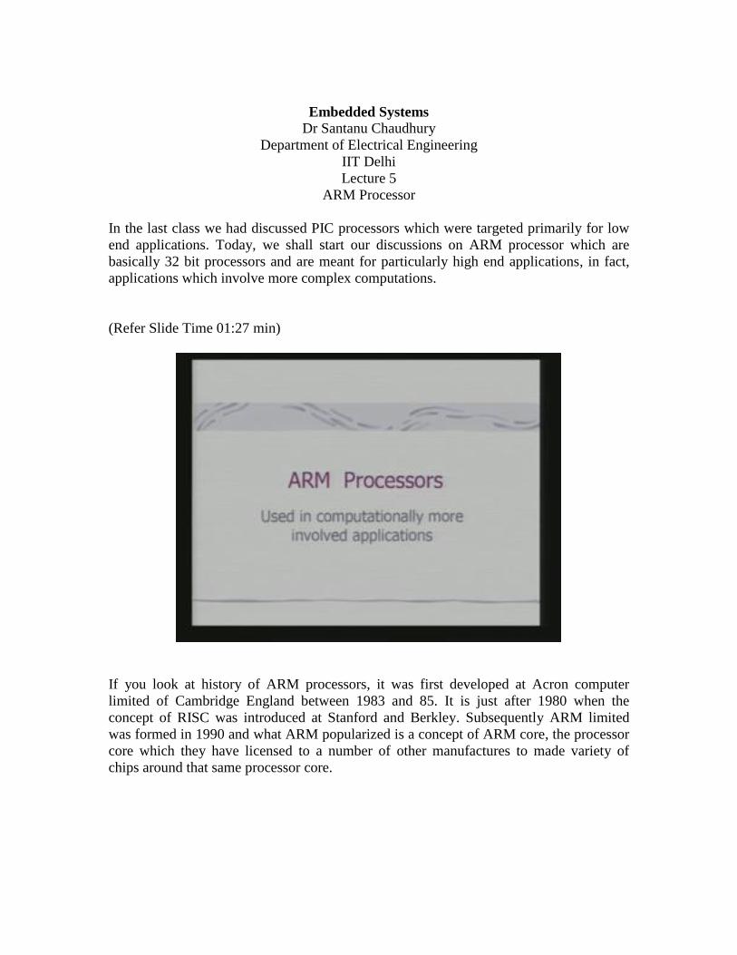
ARM Processor
In the last class we had discussed PIC processors which were targeted primarily for low
end applications. Today, we shall start our discussions on ARM processor which are
basically 32 bit processors and are meant for particularly high end applications, in fact,
applications which involve more complex computations.
(Refer Slide Time 01:27 min)
If you look at history of ARM processors, it was first developed at Acron computer
limited of Cambridge England between 1983 and 85. It is just after 1980 when the
concept of RISC was introduced at Stanford and Berkley. Subsequently ARM limited
was formed in 1990 and what ARM popularized is a concept of ARM core, the processor
core which they have licensed to a number of other manufactures to made variety of
chips around that same processor core.

(Refer Slide Time 01:54 min)
So, what we shall be starting is it is just not a family of processors but conceptually a
CPU architecture which may figure in a number of different chips intended for embedded
applications. The ARM architecture is based upon RISC architecture but it is not a purely
RISC architecture because it has been enhanced to meet requirements of embedded
applications.

(Refer Slide Time 02:28 min)
The requirements emerge for embedded applications because I need to have high code
density, low power consumption as well as low and smaller silicon footprint.
Architecturally you will find that it satisfies various conditions and properties of RISC
processors as well. It has got a large uniform register file and it basically is a load-store
architecture where data processing operations are only with registers and does not really
involve memory locations. It is basically 32 bit processor, but you will find the variants
of that as well. In fact you have got ARM processors which can support both 32 bit as
well as 16 bit operations. So, there is a 16 bit variant embedded into a 32 bit processor.
Why? We shall come to that point when you discuss thumb extensions of ARM
architecture. It has got good speed versus power consumption ratio and high code density
as needed for embedded systems. But where are its real exceptions or departure from
classical RISC architecture. In this case, you have got variety of interesting add-on
features in ARM. They have got a barrel shifter in the data path which can maximize the
hardware available on chip, usage of hardware available on chip. Then there is an auto
increment and auto decrement addressing modes to optimize program loops. This is not
very common with RISC processors. Also it supports load and store of multiple data
elements through a single instruction and subsequently you will find that there is an
interesting set of branch instructions. In these branch instructions, they are not just
individual branch instructions but this branching can be used in conjunction with other
operations. So, you have got a large variety of branching possibilities and these has also
been used maximized the execution throughput.

(Refer Slide Time 04:36 min)
So, the basic idea is that taken RISC code that is basic idea where RISC architecture, in
ARM we shall find various enhancements which have been made into it to make it more
suited for embedded applications. And these actually distinguish ARM from other typical
RISC processors. There are various variations of this architecture, in fact the whole idea
is that this architecture has undergone a number of versions and these versions have been
implemented into number of processors having distinct identities and numbers. So, here
we have listed four such versions, version 1, version 2, version 3, version 4 you will find
that initially the processor was a 26 bit addressing processor, it had no multiply or
provision for core processors. The version 2 really made a 32 bit addressing mode.
Version 3 really made it into a 32 bit addressing regis capable and version 2 included
multiply as an option. Now, this is a definite departure from PIC.

(Refer Slide Time 06:47 min)
PIC, like other simple micro-controllers simply support add and subtract operations.
Here, in this instructions set itself I have got multiply. In fact we shall see also variations
of multiply in the instruction set of all. In fact version 4 was characterized by enhanced
set of instruction and in version 4 itself they introduced what is called the thump mode
and this version is called version 4T which included a 16 bit mode. Now, this 16 bit mode
obviously implies what that given the cell memory if I can use 16 bit instructions I can
pack additional instructions. So, I can use this effectively same memory for more
instructions and thereby I can increase code density. And this is particularly useful when
you really do not require 32 bit operations. And this embedding of a 16 bit variant inside
the 32 bit architecture came in version and that is being refer to as version 4T is for
thumb. Then you have got version 5T which is superset of 4T adding new instructions
and the version 5TE add its signal processing instructions. In fact the instruction which
are targeted for signal processing applications into the basic set. In fact this is again are
departure from classical RISC concept.

(Refer Slide Time 08:44 min)
Now, these architectures have been implemented into a variety of chips. So, there are
some examples, ARM6 actually implements version 3. ARM7 which is a very popular
ARM version implements version 3 but another variant of this ARM7 ARM7TDMI this
actually implements version 4T that means it has got a thump embedded into the basic
processor. The StrongARM is version 4 implementation, but this implementation is from
Intel and not from ARM implemented. In fact it has been the point I was making that
ARM code that has been licensed to a number of manufactures and they have taken the
basic core done the appropriate modifications and designed processors for various
targeted applications. The example is StrongARM here, which Intel head maid around the
ARM core targeted for again embedded applications. ARM 9E-S this example is an
implementation of the version 5TE that is extension architecture which implements
digital signal processing instructions set and it is thought primarily targeted for embedded
system which need to process lots of digital signals like speech, video etc.
Now we shall look into the basic architecture, in fact you have seen that once we are
talking about so many variations of architecture, you will find that the ARM architecture
is not synonymous with the single organization. But there are certain commonality across
the different variants. We shall us look at this common feature before we go in to the
variants in detail in subsequent lectures.
First thing is any architecture is characterized by its data path as well as by the control
path. Our current focus will be on data path and we shall try to understand the instruction
set of ARM with reference to this core data path in this lecture.
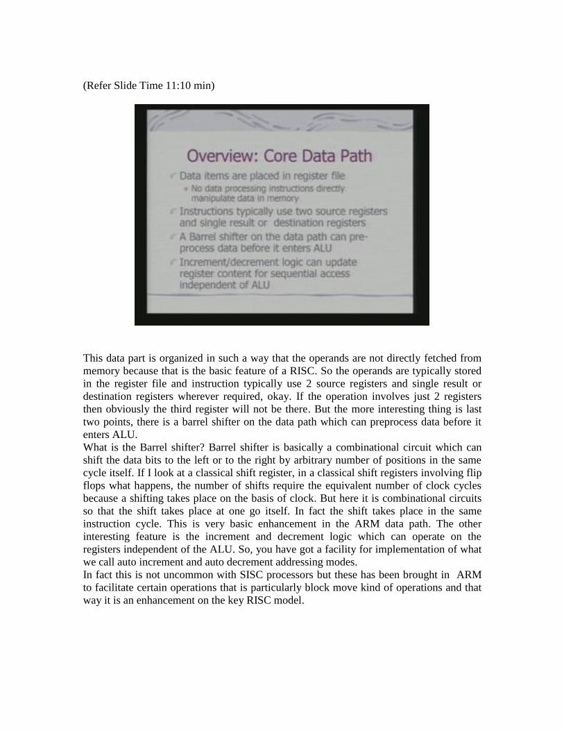
(Refer Slide Time 11:10 min)
This data part is organized in such a way that the operands are not directly fetched from
memory because that is the basic feature of a RISC. So the operands are typically stored
in the register file and instruction typically use 2 source registers and single result or
destination registers wherever required, okay. If the operation involves just 2 registers
then obviously the third register will not be there. But the more interesting thing is last
two points, there is a barrel shifter on the data path which can preprocess data before it
enters ALU.
What is the Barrel shifter? Barrel shifter is basically a combinational circuit which can
shift the data bits to the left or to the right by arbitrary number of positions in the same
cycle itself. If I look at a classical shift register, in a classical shift registers involving flip
flops what happens, the number of shifts require the equivalent number of clock cycles
because a shifting takes place on the basis of clock. But here it is combinational circuits
so that the shift takes place at one go itself. In fact the shift takes place in the same
instruction cycle. This is very basic enhancement in the ARM data path. The other
interesting feature is the increment and decrement logic which can operate on the
registers independent of the ALU. So, you have got a facility for implementation of what
we call auto increment and auto decrement addressing modes.
In fact this is not uncommon with SISC processors but these has been brought in ARM
to facilitate certain operations that is particularly block move kind of operations and that
way it is an enhancement on the key RISC model.

(Refer Slide Time 13:50 min)
So let us look at the basic ARM organization. Now what is interesting here is that this is
the register bank that we were talking about. The register bank is connected to the ALU
where two data parts one is your A bus, another data part is your B bus and this B bus
goes via the Barrel shifter. So, this Barrel shifter can actually preprocess the data which
can come from one of this source registers; and the Barrel shifter can shift to the left, shift
to the right or even rotate the data before it is fed to the ALU. Now, since all of these are
basically, ALU also, combinational circuit, Barrel shifter is also combinational circuit.
So, the entire, all these operations that is operation that ALU carries out as well as
operation that Barrel shifter carries out can take place in one cycle itself and that actually
splits up to the operation execution speed.
Now, what you find here is that I can use my register bank for generation of the address
as well, okay. In fact the PC address is, PC also is part of the register bank and that can
generate the address. As well as the other register banks, okay can be made use of for
generation for manipulation of address. Because registers are in a way symmetric they
can have both address as well as the data and they can be operated in a symmetric way.
The PC generates the address for the instruction. Now here, we have not indicated
whether it would be an Harvard or VanNeuman architecture typically, okay. So, what we
have concentrating primarily here, the data path. So, what will find in this case this
incremental block, this incremental block enables you to decrement or increment the
register values independent of the ALU. In fact the PC value can be incremented and put
back to the registers so on and so forth.
Other operations can also be done with this registers using this incremented and
decremented block. This is the instruction decode and control and that provides a control
signal and what you have shown here is this is a basic block where my address bus is 0 to

31 that means it is a 32 bit. My data buses are also 32 bits, so it is basically a 32 bit
processor. It can operate on 32 bit operands and the addresses that it generates are also 32
bit. In fact the one of the very interesting feature that you should note, not only an
interesting, a very basic concept here is, since my registers can handle data and address in
a symmetric fashion it is very easy to handle same number of bits for address and data
and use the similar kind of operations for manipulating addresses and data in the
registers. Now, let us look at this register bank because you are found that in the data part
this register bank has a very prominent role.
(Refer Slide Time 17:28 min)
All registers have to be 32 bits because my data bus is 32 bit; I am operating at 32 bit
operands as well as my addresses are also 32 bits. And how many registers are there?
Now, this is a very interesting question with respect to ARM processor. What I have said
that in user mode there are 16 data registers and 2 data registers which are visible. What it
implies, that there could be some invisible registers as well and we shall look at this
mystery slightly later on.
User mode is a common operating mode that means when you will be running your
program on ARM; typically you will be operating in user mode. And what is user mode
means it is a particular mode of operation of the processor and therefore it implies there
are other modes of operation of the processor. Data registers are typically r0 to r15 and in
fact in ARM, all registers are refer to by r followed by a number. So, here we are talking
about data registers r0 to r15 which are visible in the user mode. Out of these registers, 3
registers perform special function they are r13, r14 and r15. r13 is a stack pointer, so this
stack pointer refers to the entry point on the stack and this is critical for implementation
of a stack in the memory. r14 is a link register, now this is interesting, this is also found

in variety of other processor as well. This link register is a register where return address
is put whenever a subroutine is called. So, whenever a subroutine is called the return
address typically you will expect the model wise, we have talked about earlier in the
contest of PIC; the return address goes into stack. In PIC, it was a hardware stack
different from the program or data area. Here, we have got a single link register and in
the link register the return address is put in. Then r15 is the program counter and
obviously the current instruction what is being executed will be pointed to by the content
of r15.
(Refer Slide Time 20:09 min)
Now, depending on the context registers r13 and r14 can also be used as general purpose
registers, although this is not a very common usage because you understood that r13 and
r14 has got a special role to play. The, any instruction which use r0 can as well be used to
any other GPR, okay and in addition there are 2 status registers. CPSR, current program
status register and SPSR what is called saved program status register. These are basically
the status registers which are not data registers. So, here in this registers effectively the
status of the current execution is being captured. In fact this status can include status of
your program as well as that of the processor. The r15, the register is the, is basically the
PC, so these instructions, so this is, this will be a 32 bit wide because that will have the
address.

(Refer Slide Time 21:07 min)
And when it is operating in your 32 bit mode, that is not in the mode, all instructions will
be 32 bit and the addresses are also 32 bit and what we assume that all instructions are
word aligned. That means all 32 bit instructions start at 32 bit boundary; this is very
important, okay. And what does that imply, that implies that PC value is stored
effectively in bits from 2 to 31, bit numbers 2 to 31, with bits 1, 0 effectively undefined
or not really useful for referring to an instruction. Now, obviously this discussion refers
to one fact that my 32 bit address in ARM refers to byte locations. Each byte with
associated with a unique address so, if I am talking about 32 bit boundaries that means
effectively I am talking about what blocks of 4 bytes. So, if I have one instruction starting
at location 0 then that instruction will occupy location 0, 1, 2 as well as 3, fine. The next
instruction would be located at 4 so, therefore these 2 bits, the least significant bits of PC
that is r15 or in a way do not care for operations, okay. So, that is why we say that PC
value is effectively stored in bits from 2 to 31.

(Refer Slide Time 23:33 min)
Now, let us look at the status register CPSR. CPSR is- what is the current program status
register; it has got a number of bits. Again it will be a 32 bit register; it is not that all bits
are used at the same time. The condition code flags which occupy the higher that MSPs
that is most significant bits in the status register; they are standard flags which reflect
various arithmetic conditions. I have got negative flag if there is a negative result from
ALU which is typically the most significant bit, it is associated the most significant bit. If
it is one then it can be interpreted as a negative result when we are doing signed
arithmetic set, Z indicates 0, C is the carry and V is overflow. There is this sticky
overflow flag, this is with reference to saturation arithmetic and there is interrupt, disable
bits here which are for, there are two levels of interrupts. We shall come to that point
later on.
So, we can enable or disable these two levels of interrupts by using these 2 bits. This T
bit indicates whether you are in thump mode or not thumb mode because when we
actually have an embedded 16 bit processor into the 32 bit architecture, we shall be
making use of this T bit to know whether I am operating in the thumb mode or ordinary
32 bit mode. And rest are mode bits and these mode bits really defined what is called the
mode of processors operation. The point I was discussing in terms of registers, we are
telling that you can use about16 data registers, we can use 16 data registers in your
program and normal operation and that is user mode, that mode specified in these bits.
Now, before going into these processor modes in detail, let us briefly look at this sticky
overflow flag. What is saturation? Saturation means when we reach the maximum value
or the minimum value because of an arithmetic operation which may have overflow or
underflow. Now, when we are, when we want to have, say for example, I have got the

maximum value, it is all ones. And if I had 1 to it the actually 32 bit content would
become 0, okay.
Now, I may not like the 32 bit, 32 bit value to becomes 0,I may like it to stick to all
one’s. That is a maximum value be retained. Now, that is enabled in saturation arithmetic
and that is required for a number of signal processing tasks. In fact the architecture 5TE
has got signal processing extension and that is why this Q flag, the saturation arithmetic
flag becomes significant or important or relevant with respective to that architecture. The
processors modes, why are these processor modes are there? They are there to define
various kinds of registers; their visibility as well as rights to what we call modify CPSR
register.
So, we call the processor modes either privileged or non-privileged mode. In a privileged
mode you expect to have full read-write access to the CPSR. In a non-privileged mode
only read access to the control field of CPSR but read-write access to the condition flags.
(Refer Slide Time 26:57 min)
Now, try to understand this- what is the implication of these privileged and non-
privileged modes. In a privileged mode what can happen actually, in a privileged modes
as you can change the control bits that means you can have a full read as well as write
access of the control bits. You can actually change the processor mode, you can enable,
disable the interrupts. So, this is a privileged operation. In a non- privileged mode, these
control fields can be simply read but can not be changed, but the condition flags which
can change because of an arithmetic operation would normally reflect the status of the
arithmetic operation and that should be remain write enable even in non-privileged
modes.
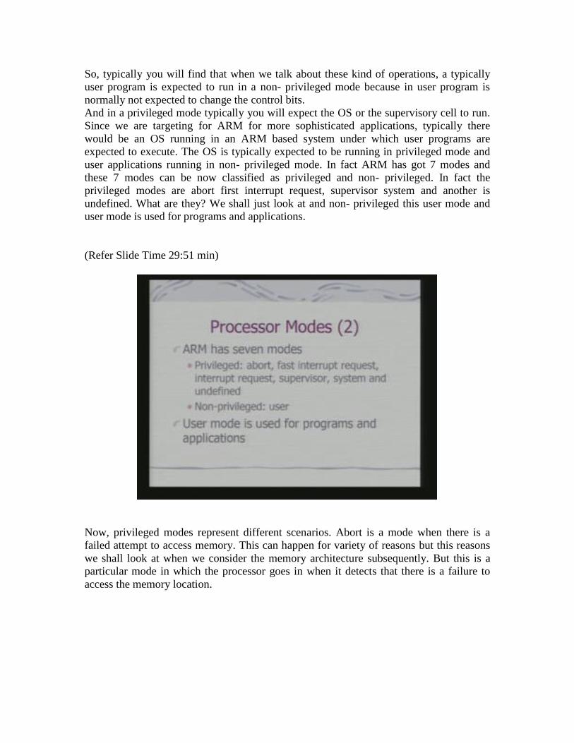
So, typically you will find that when we talk about these kind of operations, a typically
user program is expected to run in a non- privileged mode because in user program is
normally not expected to change the control bits.
And in a privileged mode typically you will expect the OS or the supervisory cell to run.
Since we are targeting for ARM for more sophisticated applications, typically there
would be an OS running in an ARM based system under which user programs are
expected to execute. The OS is typically expected to be running in privileged mode and
user applications running in non- privileged mode. In fact ARM has got 7 modes and
these 7 modes can be now classified as privileged and non- privileged. In fact the
privileged modes are abort first interrupt request, supervisor system and another is
undefined. What are they? We shall just look at and non- privileged this user mode and
user mode is used for programs and applications.
(Refer Slide Time 29:51 min)
Now, privileged modes represent different scenarios. Abort is a mode when there is a
failed attempt to access memory. This can happen for variety of reasons but this reasons
we shall look at when we consider the memory architecture subsequently. But this is a
particular mode in which the processor goes in when it detects that there is a failure to
access the memory location.

(Refer Slide Time 30:35 min)
The first interrupt request and interrupt request correspond to interrupt levels available on
ARM, okay. So, when a particular kind of interrupt occurs ARM processor goes into
other first interrupt mode or interrupt request mode.
Supervisor mode is a state in which processor goes in after reset and generally it is a
mode in which the OS kernel is suppose to operate because obviously when the processor
is reset, the first thing that its excepted to execute is a operating system code and not user
application of program. So, this is a supervisor mode in which the processor goes in when
the reset happens. The other two privileged modes are system mode and another mode is
called undefined. In a system mode, is a special version of user mode that allows full
read-write access of CPSR, okay.

(Refer Slide Time 31:33 min)
And it is also targeted for supervisory applications; many of the OS routines can be
configured to run in the system mode. The undefined mode, processer enters this
undefined mode when it encounters an undefined instruction that means when you are
trying to use an illegal op-code for undefined instruction, the instruction undefined for
particular processor, then it goes into an undefined.
So, what you have found is that these privileged modes are primarily targeted for OS
handling of special error conditions as well as that of interrupts and user mode is a mode
intended for running user applications. Now, these modes have got associated with them
a very interesting capability to manage the registers.
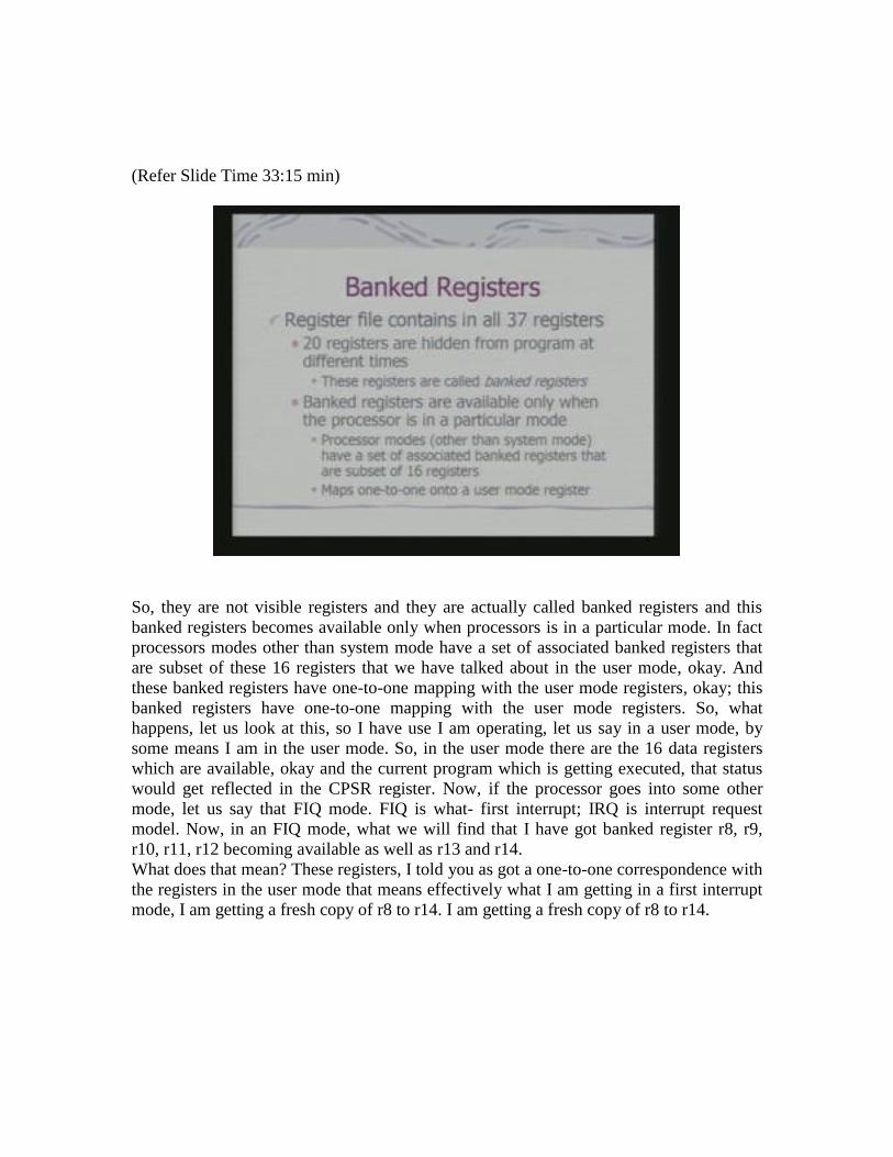
So, we go into the concept of what we call banked register in ARM architecture. ARM
has got 37 registers in all and typically 20 registers are hidden from program at different
times.
(Refer Slide Time 33:15 min)
So, they are not visible registers and they are actually called banked registers and this
banked registers becomes available only when processors is in a particular mode. In fact
processors modes other than system mode have a set of associated banked registers that
are subset of these 16 registers that we have talked about in the user mode, okay. And
these banked registers have one-to-one mapping with the user mode registers, okay; this
banked registers have one-to-one mapping with the user mode registers. So, what
happens, let us look at this, so I have use I am operating, let us say in a user mode, by
some means I am in the user mode. So, in the user mode there are the 16 data registers
which are available, okay and the current program which is getting executed, that status
would get reflected in the CPSR register. Now, if the processor goes into some other
mode, let us say that FIQ mode. FIQ is what- first interrupt; IRQ is interrupt request
model. Now, in an FIQ mode, what we will find that I have got banked register r8, r9,
r10, r11, r12 becoming available as well as r13 and r14.
What does that mean? These registers, I told you as got a one-to-one correspondence with
the registers in the user mode that means effectively what I am getting in a first interrupt
mode, I am getting a fresh copy of r8 to r14. I am getting a fresh copy of r8 to r14.

(Refer Slide Time 33:59 min)
Now, what does that imply? It implies that if I am having an interrupt service routine
which is operating in FIQ that is which is basically serving in the interrupt, in the first
interrupt mode, it can use r8, r9 to r14 without bothering about what happens to the
original content of these registers. See, we have told you that when you want to, you
know otherwise also that when you go to the interrupt service routine and if I want to
from there, if I want to come back to the original program and I have to do what, to
comeback to the correct state of computation, I need to stored the registers in the stack.
Now, storing the registers in the stack is R consisting of push a operation that will have
the overhead and that is actually the software latency for interrupt processing. In the last
class, we have looked that hardware latency, this becomes the software latency. The
moment I have got a fresh copy of this registers; see if my ISR do not use any other
register than this, I really do not meet to push this registers onto stack. So, I can minimize
my software latency and in fact that is a reason why this mode is called first interrupt
mode. In other one, the interrupt request mode what you have is simply r13 and r14 fresh
copy is generated, okay. So, other registers the copy is not generated. So, other registers,
you need to save if you are using them; so obviously it is not as fast as that of a first
interrupt mode because here there will be some amount of software latency which will be
involved. The similar thing is true for the other modes- the supervisory mode undefined,
abort, all these modes have got a copy of r39, r14 but other register the fresh copy is not
generated.
So, these original user mode registers have to be used; if they are to be retained they have
to be safe in memory. So, what happens in case of CPSR? Now, corresponding to CPSR

what you get in these modes what are called SPSR. So, what is the SPSR- save program
state register. So, CPSR is copied into SPSR which becomes available in FIQ mode. So,
when I return from this mode to say user mode, I have to take this content of SPSR back
to CPSR because CPSR would be storing the current status; so when I am going back I
should have the current status of the computation back with me. So, pictorially what we
say here on the abort SPSR is each privileged mode except system mode has associated
with it a save program status register or SPSR.
(Refer Slide Time 38:07 min)
This SPSR is used to save the status of CPSR when the privileged mode is entered in
order that the user state can be fully restored when the user process is resumed; this is
particularly the job of SPSR. So, now if you summarize what we have saved that in the
user mode I have got these 16 registers as well as CPSR.
In FIQ mode what I have got, I have got same r0 to r7 registers as that of user mode but a
fresh copy of these registers, okay. Similar thing in IRG; IRG have got I can use the
registers same as that of r0 to r12 that fresh copy of r13 and r1,4 okay and CPSR is
showing here. So, this CPSR is copied into SPSR.

(Refer Slide Time 38:36 min)
But, obviously in FIQ mode I got to have a CPSR which will reflect the state of the
processors in that mode during execution of that program, okay. So, effectively what we
are telling is that in these modes if you have writing onto this registers I shall overwrite
the original data. See, if I have to save this data, if I have to get this data back, I need to
save it in the stack. But in case of FIQ, I get a fresh copy of registers; so I need not save
this register save on to the stack and thereby have reduced software latency.

(Refer Slide Time 40:18 min)
The more changes can be made by directly writing onto CPSR or by hardware when the
processor responds to exception or interrupt. And to return to user mode, a special return
instruction is used that instructs the core to restore the original CPSR and banked
registers. The ARM memory organization, in fact ARM can be configured either in little
endian form or in big endian form.
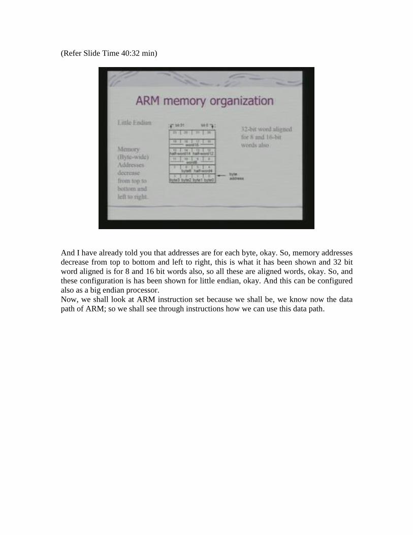
(Refer Slide Time 40:32 min)
And I have already told you that addresses are for each byte, okay. So, memory addresses
decrease from top to bottom and left to right, this is what it has been shown and 32 bit
word aligned is for 8 and 16 bit words also, so all these are aligned words, okay. So, and
these configuration is has been shown for little endian, okay. And this can be configured
also as a big endian processor.
Now, we shall look at ARM instruction set because we shall be, we know now the data
path of ARM; so we shall see through instructions how we can use this data path.
(Refer Slide Time 41:21 min)
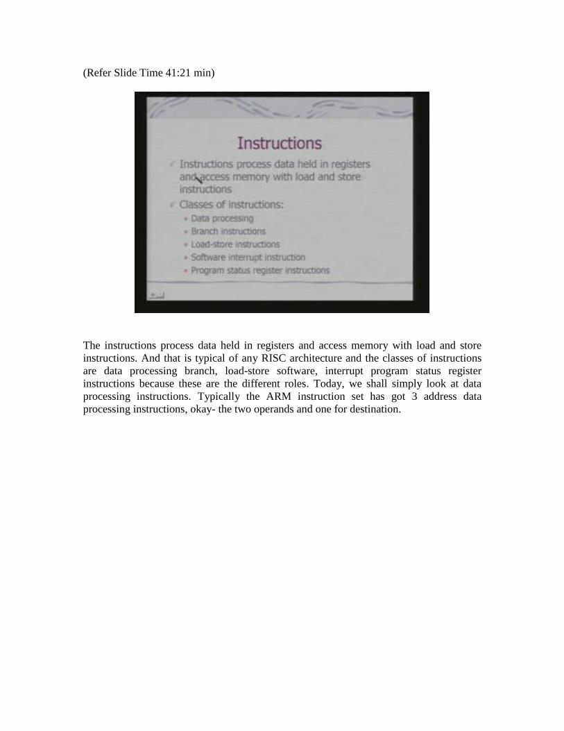
The instructions process data held in registers and access memory with load and store
instructions. And that is typical of any RISC architecture and the classes of instructions
are data processing branch, load-store software, interrupt program status register
instructions because these are the different roles. Today, we shall simply look at data
processing instructions. Typically the ARM instruction set has got 3 address data
processing instructions, okay- the two operands and one for destination.

(Refer Slide Time 42:29 min)
The other interesting feature of the instruction set is that you can do a conditional
execution of each instruction. That means depending on certain condition, you can decide
whether to execute an instruction or not. In fact this is a very special kind of branch
instructions and I have told you, this is an enhancement in the RISC architecture to
increase the computation throughput. The Barrel shifter enables shift and ALU together;
so we shall have that enhancement of instruction set to do this operations and the other
interesting thing we shall look at subsequently that you can actually increase the
instruction set of the processor by adding on co-processors.
And how to do that, that will be a very interesting feature for ARM architecture. Now,
before we look into data processing instructions, we need to know what kind of data
types are supported in ARM. Obviously ARM is the 32 bit processor.
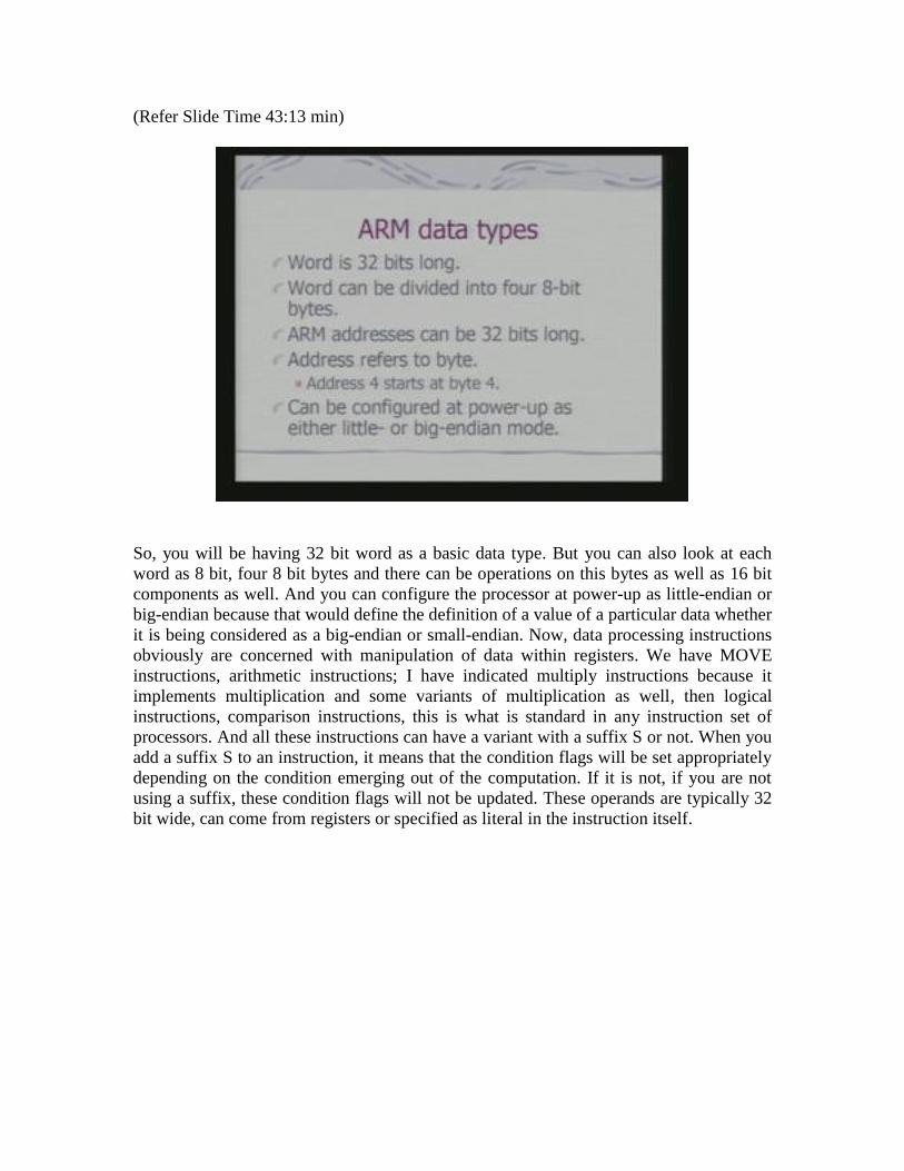
(Refer Slide Time 43:13 min)
So, you will be having 32 bit word as a basic data type. But you can also look at each
word as 8 bit, four 8 bit bytes and there can be operations on this bytes as well as 16 bit
components as well. And you can configure the processor at power-up as little-endian or
big-endian because that would define the definition of a value of a particular data whether
it is being considered as a big-endian or small-endian. Now, data processing instructions
obviously are concerned with manipulation of data within registers. We have MOVE
instructions, arithmetic instructions; I have indicated multiply instructions because it
implements multiplication and some variants of multiplication as well, then logical
instructions, comparison instructions, this is what is standard in any instruction set of
processors. And all these instructions can have a variant with a suffix S or not. When you
add a suffix S to an instruction, it means that the condition flags will be set appropriately
depending on the condition emerging out of the computation. If it is not, if you are not
using a suffix, these condition flags will not be updated. These operands are typically 32
bit wide, can come from registers or specified as literal in the instruction itself.

(Refer Slide Time 44:40 min)
That means I can have registers as well as immediate operands. The second operand can
be sent via barrel shifter and 32 bit result is again placed in register only other cases that
when you really do a 32 bit multiplication you generate 64 bit result which can go into
multiple registers. So, this is an example of a move instruction. So move will obviously
involve two operands, okay and I have shown you here, this is your destination register
and N can be immediate value or source register. A simple example is r7 to r5; it means
that I am moving content of r5 to r7. There is an interesting variant of move which is
MVN the move negative. So, what you move? You move into Rd not of the 32 value
from source, okay. So, this N can be a register, can also be an immediate value; so what
you move in is not of that value into the destination.

(Refer Slide Time 45:09 min)
Now, you can use barrel shifter with the move instruction, okay and this barrel shifter can
shift left, shift right, rotate right by fixed number of bits, okay. And what does it therefore
help in, you can do a fast multiply and division and let us look at a simple example. Here,
what I have done? I have specified you move content of r5 to r7 but I have said that you
do a logical shift left by 2 positions; #2 indicates that immediate value 2.

(Refer Slide Time 46:08 min)
So, it multiplies the content of r5 by 4 and puts the result in r7. That means effectively
what I have done, combine two operations into a single instruction and that is the basic
role that barrel shifter plays. So, effectively this is the whole picture; again I am
repeating, we have already seen that on the data path. So, I have got a barrel shifter and
this operand 2 comes to barrel shifter, it can be an immediate value of the operand. And I
would specify the number of positions that I need to shift as part of the instruction itself.

(Refer Slide Time 46:51 min)
It can be an immediate value or it can be specified in a register as well. Similarly, we
have arithmetic instructions, simple arithmetic instructions implement your 32 bit
addition and subtractions. Obviously, in this case I shall have 3 operands, 2 source set
and destination.
(Refer Slide Time 47:20 min)

Here, I have given some example of subtraction instructions. So, I have got here the r0,
sub r0, r1 and r2, it subtracts the value stored in r2 from that of r1 and the result is stored
in r0. In this case, this is an example of subtraction using an immediate operand and here
I have used suffix S that means the result, that is the effect emerging out of this
computation will be reflected in the bits of the CPSR. But that is not true essentially in
this case of, in this instruction. Now, we can use these operations with Barrel shifter; the
moment we use them with Barrel shifter, then the possibilities also increases. So, look at
this- this is an example of an ADD instruction and what I have done, I have added
content of r1, okay and what I have written here I want to again do a shift, shift by one
position.
(Refer Slide Time 48:33 min)
So if I shift by one position, it is effectively means what, it is multiplied by 2. And then I
am adding to r1, adding to itself and putting the result back to r0, so effectively I am
multiplying the content of r1 by 3 and putting the result in r0, okay. So, these are the
various possibilities which can be there. So, you can use the Barrel shifter and these
operations with all of these arithmetic instructions. Next, we have multiply instruction, in
fact multiply as a block is implemented in ARM, okay. And this multiply can be looked
at in two forms- one is called long multiply; in case of long multiply you are expected to
generate 64 bits results. Otherwise, the result is a 32 bit result. So, here we have given an
example where we are telling that you multiply r1 and r2 and put the result back to r0.
This is a case of a 32 bit multiplication that is the result expected is 32 bit, so that it can
be accommodated in r0. This is the case of a long multiplication and case of a long
unsigned multiplication, okay.

(Refer Slide Time 50:30 min)
So you multiply the results r2 and r3 and the result is stored in r0 and r1, okay.
The number of cycles taken for execution of multiply instruction depends upon processor
implementation, okay. So, that will be architecture dependent and you also have other
than unsigned, you have got signed multiplication where the sign bit is taken care of
while doing the multiplication. So, sign you get sign long multiplication; but along with
multiplication there is another very interesting instruction which is multiply and
accumulator- what is called MLA.

(Refer Slide Time 51:14 min)
Now, in this case what happens? I have shown the operations, if you look at here what
happens here and actually in this case, okay I can, this an MLA this is not a long MLA.
This is an MLA with, which is expected to produce 32 bit result. In this case what
happens you actually multiply Rm into Rs, this is added with Rn, that is another register
content and the register result is stored in Rd, the destination register. And where do you
expect MLA operation, a very simple operation is when you do a conclusion, a simple
operation is conclusion, when you do convolution, you actually multiply and add and if I
have to implement convolution which is very basic operation for a large number of signal
processing task then MLA becomes a very useful instruction. And that is basically the
motivation for implementing MLA as an instruction in the ARM processor itself.
The other variant of MLA is unsigned long MLA; so here you have got this, these 2
registers will contain the final result and in this case content of this registers is added with
the product. And this product is expected to be a 64 bit product and so this 64 bit product
is added with this 64 bit content of the registers and that result is stored here.

(Refer Slide Time 52:41)
There are logical instructions AND, OR, EX-OR, bit clear. In fact bit clear is a very
interesting instruction; in this case, this r2 I have given an example here BIC r0, r1, r2.
Now, r2 contains a binary pattern, for every binary one in r2 clears a corresponding bit
location in register r1. So, that means I can specify a bit mask, I can specify a bit mask in
r2, depending on that bit mask the bits of r1 will be cleared and the result will be stored in
r0, okay. So, this is obviously, this instruction is obviously useful in manipulating status
flags as well as interrupt masks. And it is something like that in bit manipulation facility.
Compare instructions are another set of instruction. So, I have got simple compare, then I
have got TEQ for equality and this TST, another is TST.
So, you will find that depending on the operation, I have given an example with
involving registers r0 and r9. So, depending on the instruction involved, in this case of a
compare, a subtraction is done and depending on the result of the subtraction the flags are
affected but the content of registers are not affected.

(Refer Slide Time 53:39 min)
In case of TEQ, there is an ex-or operation, bit-wise ex-or operation between content of
r0 and r9 and flags are accordingly changed as it gets reflected on the basis of the result,
but the content of r0 and r9 is not changed. This is a similar thing and in this case, you
use endian and not ex-or. So, these are the typical comparisons instructions available in
R. So, what we have seen today, we have studied very basics of ARM architecture; ARM
architecture is much more complex then what we have looked at today. We have
understood the different modes of operation of the processor. We have examined the data
path in some detail and discussed the basic data processing instructions.

(Refer Slide Time 54:52 min)
We shall look at other instructions- branching instructions, then software interrupt
instruction, the processors status register manipulation instruction and the other aspects of
this architecture in subsequent lectures.