embedded pitch adapters a high-yield interconnection solution for strip sensors m. ullán, c. fleta,...
TRANSCRIPT

Embedded Pitch Adapters a high-yield interconnection solution for strip sensors
M. Ullán, C. Fleta, X. Fernández-Tejero, V. Benítez
CNM (Barcelona)

Miguel Ullán (CNM-Barcelona) RD50 meeting (Santander) – Jun 2015 2
· Motivation an proposal
· First proof of concept
· New designs
· Cint tests
· New sensors batch
· Preliminary results
· Conclusions & future work
Outline

Miguel Ullán (CNM-Barcelona) RD50 meeting (Santander) – Jun 2015 3
· Interconnection in next generation HEP experiments Larger sensors Smaller electronics More channels in both Direct wire-bonding preferred Production time constrains Bonding yield and reliability is critical
Motivation
Direct wire-bonding in a prototype End-Cap module
from DESY Berlin
ATLAS case:• Wafers: 6 inches to 8 inches• ~5000-10000 channels per sensor• 250 channels per chip• Total: ~120 million channels
(ITk)• 3 years production• 15 assembly sites• ~8000 wire-bonds per site per day
Miguel Ullán (CNM-Barcelona) RD50 meeting (Santander) – Jun 2015 4
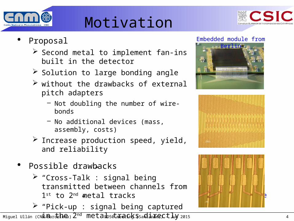
· Proposal Second metal to implement fan-ins built in the
detector Solution to large bonding angle without the drawbacks of external pitch adapters
– Not doubling the number of wire-bonds
– No additional devices (mass, assembly, costs)
Increase production speed, yield, and reliability
· Possible drawbacks “Cross-Talk”: signal being transmitted between
channels from 1st to 2nd metal tracks “Pick-up”: signal being captured in the 2nd metal
tracks directly from the bulk Noise: due to increased strip capacitance Efficiency: possible loss of CCE? Yield: reduced sensor yield
Motivation
Embedded modulefrom Berlin
Embedded module from Berlin

Miguel Ullán (CNM-Barcelona) RD50 meeting (Santander) – Jun 2015 5
First Embedded-PA· Implemented in some of the
“petalet” prototype wafers 4’’ Prototype of the ATLAS ITk
End-Cap modules
· 2 metal (Al/Cu) layers
· 1 micron inter-metal oxide layer
· “Basic” design
· Cross-talk tests Laser tests
Signal readout in every channel
No signal seen in crossing channels
M. Ullan, et al. "Embedded Pitch Adapters for the ATLAS Tracker Upgrade", NIM A, vol. 732, pp. 178-181, 2013
Miguel Ullán (CNM-Barcelona) RD50 meeting (Santander) – Jun 2015 6
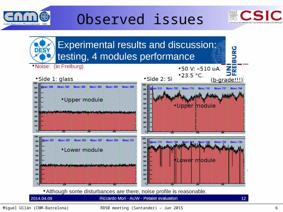
Observed issues

Miguel Ullán (CNM-Barcelona) RD50 meeting (Santander) – Jun 2015 7
New Embedded PA· New designs and technology tests
Modified designs
Narrower second-metal tracks
Thicker inter-metal layer
· Challenges: Keep low area fill ratio
and technology yield
Reduce interstrip capacitance (Cint)
Noise
“Equalize” Cint/Noise
Reduce total coupling…– with 1st metal: Cross-talk
– with bulk: Pick-up
Reduce eficiency loss
Miguel Ullán (CNM-Barcelona) RD50 meeting (Santander) – Jun 2015 8
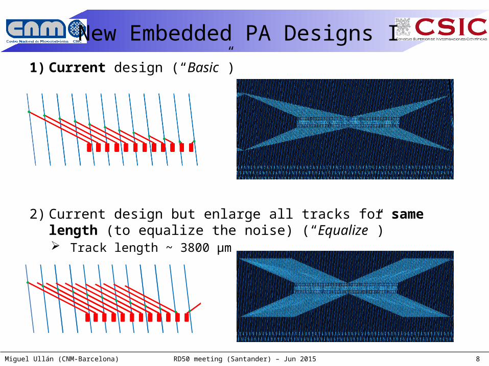
New Embedded PA Designs I1) Current design (“Basic”)
2) Current design but enlarge all tracks for same length (to equalize the noise) (“Equalize”) Track length ~ 3800 μm

Miguel Ullán (CNM-Barcelona) RD50 meeting (Santander) – Jun 2015 9
New Embedded PA Designs II3) Varying angle, similar track length (except at the two extremes) (“Varying”)
Angle ~ 3º Equalized Track Length ~ 2400 ± 200 μm

Miguel Ullán (CNM-Barcelona) RD50 meeting (Santander) – Jun 2015 10
New Embedded PA Designs III4) Rectangular to strips in between them (on top of p-stop) (“Rectangular-A”)
Equalized Track Length 1500 μm < L < 3000 μm
5) Rectangular to strips on top of them (“Rectangular-B”) Equalized Track Length 1500 μm < L < 3000 μm
Miguel Ullán (CNM-Barcelona) RD50 meeting (Santander) – Jun 2015 11
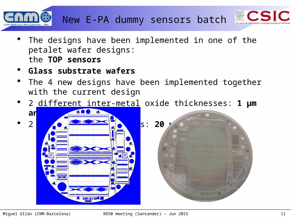
New E-PA dummy sensors batch· The designs have been implemented in one of the petalet wafer designs:
the TOP sensors· Glass substrate wafers· The 4 new designs have been implemented together with the current design· 2 different inter-metal oxide thicknesses: 1 μm and 4 μm · 2 different track widths: 20 μm and 10 μm
Miguel Ullán (CNM-Barcelona) RD50 meeting (Santander) – Jun 2015 12
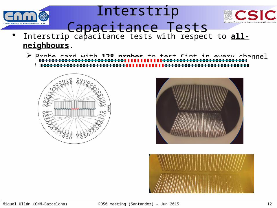
Interstrip Capacitance Tests· Interstrip capacitance tests with respect to all-neighbours.
Probe card with 128 probes to test Cint in every channel with all the rest grounded
Cint test: – one probe signal input,
rest probes: grounded
– Sensor Biased: 100 V
– 100 kHz, 100 mV, parallel mode

Miguel Ullán (CNM-Barcelona) RD50 meeting (Santander) – Jun 2015 13
Cint Test Results· Basic vs. Equal
Cint
Channel number
Cint=1.8±0.4 pFCint=0.8±0.3 pF
Miguel Ullán (CNM-Barcelona) RD50 meeting (Santander) – Jun 2015 14
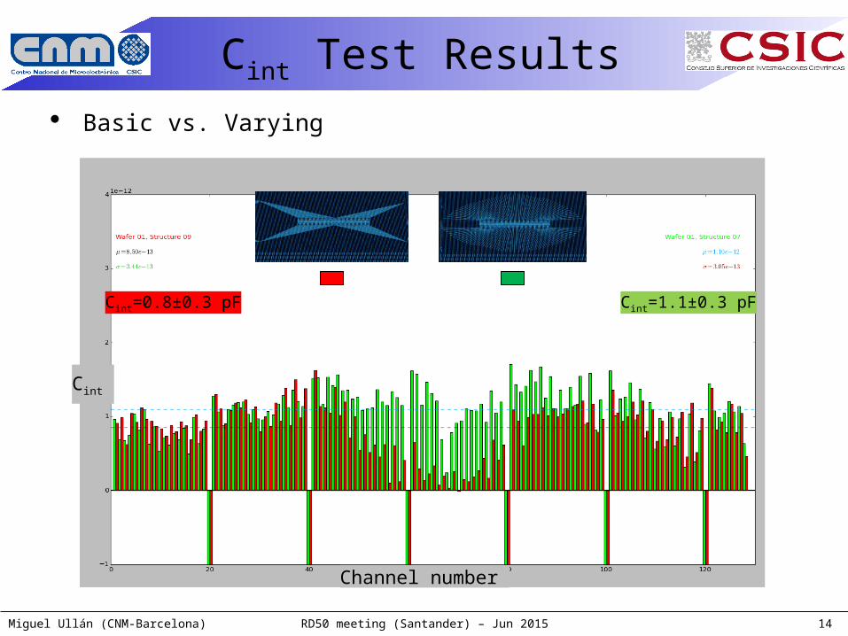
Cint Test Results· Basic vs. Varying
Cint
Channel number
Cint=1.1±0.3 pFCint=0.8±0.3 pF

Miguel Ullán (CNM-Barcelona) RD50 meeting (Santander) – Jun 2015 15
Cint Test Results· Rec-A vs. Rec-B
Cint
Channel number
Cint=2.2±0.8 pFCint=1.2±0.3 pF
Miguel Ullán (CNM-Barcelona) RD50 meeting (Santander) – Jun 2015 16
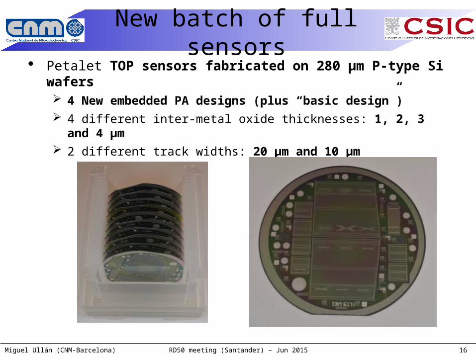
New batch of full sensors· Petalet TOP sensors fabricated on 280 μm P-type Si wafers
4 New embedded PA designs (plus “basic design”) 4 different inter-metal oxide thicknesses: 1, 2, 3 and 4 μm 2 different track widths: 20 μm and 10 μm

Miguel Ullán (CNM-Barcelona) RD50 meeting (Santander) – Jun 2015 17
Technology10 µm tracks
20 µm tracks

Miguel Ullán (CNM-Barcelona) RD50 meeting (Santander) – Jun 2015 18
Technology· Technology parameters (e.g. wafer bow) continuously monitored during
the fabrication
· Wafers suffer stress due to the TEOS deposition – limit to the achievable
thickness of the inter-metal oxide

Miguel Ullán (CNM-Barcelona) RD50 meeting (Santander) – Jun 2015 19
Via resistance and yield· Daisy-chain test structure
Up to 200 via contacts tested in two wafers:
1 µm and 3 µm inter-metal SiO2
2 daisy-chains tested per wafer
No fail seen good yield
Average via resistance:
Rvia = 0.151 ± 0.005 Ω Per via resistance
number of vias
0 50 100 150 200
R/via (ohm
)
0,0
0,2
0,4
0,6
0,8
1,0
1,2
1,4
1m - 1 1m - 23m - 13m - 2
Inhomogeneus etching of the inter-metal oxide

Miguel Ullán (CNM-Barcelona) RD50 meeting (Santander) – Jun 2015 20
BASIC vs. VARYING; 20 µm
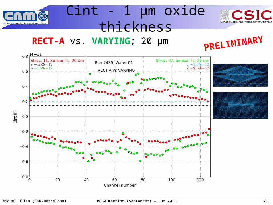
Cint - 1 µm oxide thickness
PRELIMINARY
Miguel Ullán (CNM-Barcelona) RD50 meeting (Santander) – Jun 2015 21
RECT-A vs. VARYING; 20 µm
Cint - 1 µm oxide thickness
PRELIMINARY

Miguel Ullán (CNM-Barcelona) RD50 meeting (Santander) – Jun 2015 22
BASIC; 10 µm vs. 20 µm
Cint - 1 µm oxide thickness
PRELIMINARY

Miguel Ullán (CNM-Barcelona) RD50 meeting (Santander) – Jun 2015 23
RECT-A; 10 µm vs. 20 µm
Cint - 1 µm oxide thickness
PRELIMINARY
Miguel Ullán (CNM-Barcelona) RD50 meeting (Santander) – Jun 2015 24
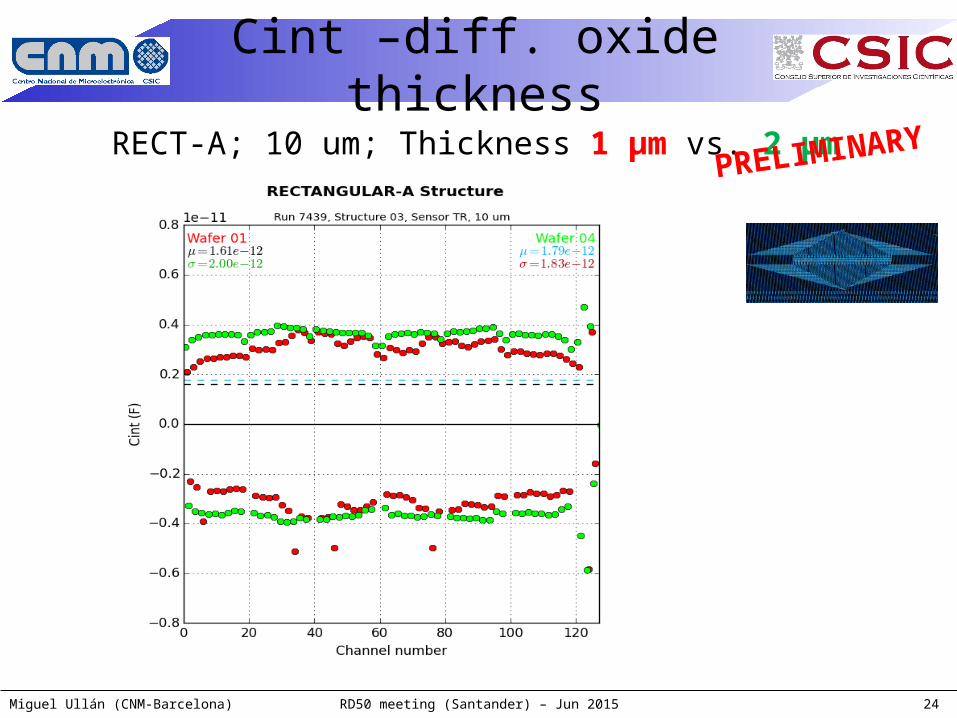
RECT-A; 10 um; Thickness 1 µm vs. 2 µm
Cint –diff. oxide thickness
PRELIMINARY

Miguel Ullán (CNM-Barcelona) RD50 meeting (Santander) – Jun 2015 25
Proposal of double-metal strip sensor technology to improve interconnection in
large HEP experiments
Initial fabrication demonstrated the concept and revealed some weaknesses
Irregular noise problem faced
New optimized designs and technology
First sensors fabricated with new designs and technology
All-neighbours interstrip capacitance tests to estimate the noise
Future work Assembly of full modules (at DESY Berlin)
Noise tests and correlation with Cint values
Test beam with modules (diamond, DESY)– Cross-talk, pick-up, Efficiency-loss
Irradiation of sensors and repeat tests
Conclusions & future work