electrostatic discharge (esd) white paper · transistor-based flat panel displays. however, esd...
TRANSCRIPT

May 2016 EOS/ESD Association, Inc.
EOS/ESD Association, Inc. 7900 Turin Rd., Bldg. 3, Rome, NY 13440 [email protected] 315-339-6937
Copyright © 2016 EOS/ESD Association, Inc. - 1 -
Electrostatic Discharge (ESD) Technology Roadmap – Revised May 2016
1.0 SYNOPSIS
This document is divided into two main sections. The first provides estimates of future ESD thresholds of semiconductor devices and their potential impact on ESD control practices. These levels are strongly technology and design dependent and need to be periodically revised in the context of advances in the electronics industry. The threshold estimates discussed in this roadmap are intended to reflect the prevailing trends in semiconductor technology as viewed by selected industry leaders. As in previous versions of this document, the emphasis is the integrated circuit (IC) industry. Other major electronics industry segments are also experiencing an increase in ESD sensitivities (lowering of ESD thresholds). Some examples are magneto-resistive (MR) heads (disk read/write heads), optoelectronics (light emitting diodes, lasers and photodiodes) and thin-filmed-transistor-based flat panel displays. However, ESD trend information is not usually readily available for these types of devices and the often standardized ESD tests are not defined or broadly applied.
The thresholds are presented in this document in the form of “roadmaps” of estimated decreases in thresholds by year. These projections are intended to provide a view of future device protection limitations driven by circuit performance requirements and technology scaling effects. It also provides a common view of expected device ESD performance variations as viewed by device (IC) suppliers and original equipment manufacturers (OEMs), i.e. users. Finally, these trends point to the need for continued improvements in ESD control procedures and compliance. Some linkage of these trends to process capability is also discussed, as is progress in other ESD events characterization (system-level, charged-board events, and cable discharge events). The second section contains information on trends in device testing and characterization from the ESDA and ESDA/JEDEC teams working on these methods and finishes up with a discussion on novel technology trends.
2.0 DEVICE THRESHOLD TRENDS
2.1 Overview
In the late 1970s, ESD became a problem in the electronics industry. Low threshold level ESD events from people were causing device failures and yield losses. As the industry learned about this phenomenon, both device design improvements and process changes were made to make the devices more robust and processes more capable of handling these devices.
During the 1980s and early 1990s, device engineers, after going through a learning curve, were able to create protection structures that could withstand higher levels of ESD stress and thus made devices less sensitive to ESD events. Both device engineers and circuit designers were able to identify key technology parameters and design techniques that helped them develop more robust devices.
However, in the mid to late 1990s the requirements for increased performance (devices that operate at 1 GHz and higher) and the increase in the density of circuits (Moore’s Law) on a device caused problems for traditional ESD protection circuits. This was exacerbated with the continued scaling of the technologies toward sub-100 nm feature sizes in order to achieve higher density and performance. The situation became worse with the advent of IC chips with sub-50 nm technologies which were rapidly coming into production. For example, with the demand for high speed internet operations, large, high pin count (> 1000 pins), packaged devices now contain high speed serial link (HSS) input/outputs (IOs) that need to operate at 10-15 gigabit per second (Gbs) and these are already reaching 20-30 Gbs for the next generation at 22 nm and 18 nm technology nodes. As a result, both human body model (HBM) and charged device model (CDM) target levels had to be lowered to accommodate these features. Also, radio frequency (RF) circuit operations will continue their growth, with these pins only tolerating a very low capacitive load from ESD cells. Due to these trends, ICs are expected to become even more sensitive to ESD events in the years 2020 and beyond. Therefore, it is anticipated that the prevailing trend will continue to be increased circuit performance at the expense of the designed ESD protection levels.
Copyright 2016 by EOS/ESD Association, Inc. (all rights reserved). Downloaded from the EOS/ESD Association, Inc. website, www.esda.org.
NO FURTHER REPRODUCTION OR DISTRIBUTION PERMITTED.

May 2016 EOS/ESD Association, Inc.
EOS/ESD Association, Inc. 7900 Turin Rd., Bldg. 3, Rome, NY 13440 [email protected] 315-339-6937
Copyright © 2016 EOS/ESD Association, Inc. - 2 -
For future device qualification, HBM and CDM should fulfill the necessary requirements. Further, as documented in White Paper 1 from the Industry Council, Machine Model (MM) protection is intrinsic to HBM and does not need to be done for qualification [1]. Thus, a separate technology roadmap for MM would be obsolete. However, this information in no way diminishes the importance of proper grounding of any conductor which may come in contact with ESD sensitive devices and the importance of avoiding hard conductor-conductor discharges1. It should also be pointed out that conductor-to-device discharges are not well represented by the MM device test. The CDM method gives a better representation of these events. In summary, although control of isolated conductors is important for a factory environment, the reported MM threshold values have no relevance. HBM and CDM levels are the important criteria for technology scaling.
2.2 Device ESD Threshold Roadmaps
The following graphs show the device ESD design sensitivity trends based on the most relevant and important ESD models used by device manufacturers as part of the device qualification process: HBM and CDM. The sensitivity limits are a projection by engineers from leading semiconductor manufacturers.
2.2.1 Human Body Model (HBM) Roadmap
The projections for HBM design (typical min and max) are indicated in Figure 1. Although design improvements were made from 1978 through 1993, representing a learning curve process, advanced circuit performance effects started to take place around this time, eventually degrading the levels. The max levels represent what is typically possible from technology scaling and min levels represent the constriction coming from meeting the circuit performance demands.
Figure 1: Overall Human Body Model Sensitivity Limits Projections
Since the overall full time-line graph is difficult to read, Figure 2 presents a zoomed-in look at 2010 and beyond. Also shown in Figure 2 is the estimated ESD control capability for HBM during the same time period based on the levels of HBM controls which may be in place. It is significant that
1 Hard discharges can also occur between low conductivity non-metallic materials such as carbon-loaded plastics.
HBM Roadmap (Typical Min – Max)
1980 1985 1990 1995 2000 2005 2010
4 kV
2 kV
6 kV
0 V
1 kV
20151975
De facto
Target Level
Current Target
Level
2020
500 V
Projected Target
Level
Copyright © 2016 ESD Association Copyright © 2016 EOS/ESD Association, Inc.
Copyright 2016 by EOS/ESD Association, Inc. (all rights reserved). Downloaded from the EOS/ESD Association, Inc. website, www.esda.org.
NO FURTHER REPRODUCTION OR DISTRIBUTION PERMITTED.
May 2016 EOS/ESD Association, Inc.
EOS/ESD Association, Inc. 7900 Turin Rd., Bldg. 3, Rome, NY 13440 [email protected] 315-339-6937
Copyright © 2016 EOS/ESD Association, Inc. - 3 -
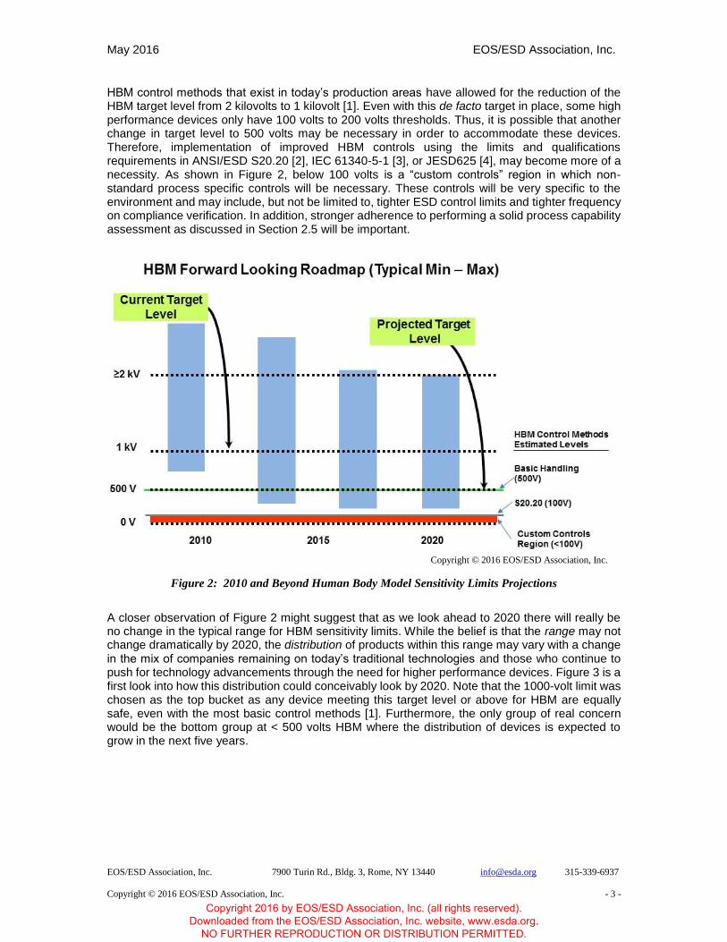
HBM control methods that exist in today’s production areas have allowed for the reduction of the HBM target level from 2 kilovolts to 1 kilovolt [1]. Even with this de facto target in place, some high performance devices only have 100 volts to 200 volts thresholds. Thus, it is possible that another change in target level to 500 volts may be necessary in order to accommodate these devices. Therefore, implementation of improved HBM controls using the limits and qualifications requirements in ANSI/ESD S20.20 [2], IEC 61340-5-1 [3], or JESD625 [4], may become more of a necessity. As shown in Figure 2, below 100 volts is a “custom controls” region in which non-standard process specific controls will be necessary. These controls will be very specific to the environment and may include, but not be limited to, tighter ESD control limits and tighter frequency on compliance verification. In addition, stronger adherence to performing a solid process capability assessment as discussed in Section 2.5 will be important.
Figure 2: 2010 and Beyond Human Body Model Sensitivity Limits Projections
A closer observation of Figure 2 might suggest that as we look ahead to 2020 there will really be no change in the typical range for HBM sensitivity limits. While the belief is that the range may not change dramatically by 2020, the distribution of products within this range may vary with a change in the mix of companies remaining on today’s traditional technologies and those who continue to push for technology advancements through the need for higher performance devices. Figure 3 is a first look into how this distribution could conceivably look by 2020. Note that the 1000-volt limit was chosen as the top bucket as any device meeting this target level or above for HBM are equally safe, even with the most basic control methods [1]. Furthermore, the only group of real concern would be the bottom group at < 500 volts HBM where the distribution of devices is expected to grow in the next five years.
Copyright © 2016 EOS/ESD Association, Inc.
Copyright 2016 by EOS/ESD Association, Inc. (all rights reserved). Downloaded from the EOS/ESD Association, Inc. website, www.esda.org.
NO FURTHER REPRODUCTION OR DISTRIBUTION PERMITTED.

May 2016 EOS/ESD Association, Inc.
EOS/ESD Association, Inc. 7900 Turin Rd., Bldg. 3, Rome, NY 13440 [email protected] 315-339-6937
Copyright © 2016 EOS/ESD Association, Inc. - 4 -
Figure 3: Forward Looking Human Body Model Sensitivity Distribution Groups
2.2.2 Charged Device Model (CDM) Roadmap
The technology impact on CDM not only comes from the required IO speeds but also from package size effects. Larger packages will experience higher discharge currents at a given stress voltage level. Although the chart does not cover all IC package types, Figure 4 illustrates the combined IO design and package effect as projected for a 22 nm technology node. The color scheme adopted in Figure 4 is based on the validation that 250 volts CDM is safe for production areas [5]. This map would change as the technology is further scaled or package sizes become even larger. For
example, note that for today’s packages of 3000 pins (~3000-3500 mm2) or more (not uncommon for a microprocessor) in a land grid array (LGA) or ball grid array (BGA), high speed IOs at the 22 nm node would barely meet a CDM target level of 125 volts. An additional package effect, decreasing thickness, was not included here for simplicity.
2010-2015 By 2020
> 1000 V
500 - 1000 V
< 500 V< 500 V
500 - 1000 V
> 1000 V
Cop
yri
gh
t ©
201
6 E
OS
/ES
D A
ssoci
atio
n,
Inc.
Copyright 2016 by EOS/ESD Association, Inc. (all rights reserved). Downloaded from the EOS/ESD Association, Inc. website, www.esda.org.
NO FURTHER REPRODUCTION OR DISTRIBUTION PERMITTED.

May 2016 EOS/ESD Association, Inc.
EOS/ESD Association, Inc. 7900 Turin Rd., Bldg. 3, Rome, NY 13440 [email protected] 315-339-6937
Copyright © 2016 EOS/ESD Association, Inc. - 5 -
Figure 4: Combined Projected Effects of Technology Node (22 nm), IO Design,
and IC Package Size on CDM
Based on the above, the projections for CDM sensitivity levels (typical min and max) are indicated in Figure 5. As shown in the figure, the CDM target has been modified to 250 volts, reduced from the previous 500 volts. But a target of 125 volts will be realistically needed in the future.
Figure 5: Overall Charged Device Model Sensitivity Limits Projections
Pa
ck
ag
e
De
sig
nH
SS
RF
Dig
ita
l IO
10 100 1000 10000
252500250
DIP QFP TQFP BGA
750V
NUMBER OF PINS
PACKAGE AREA MM 2
500V 400V 300V 250V
1
400V 300V 250V
250V400V 300V
High Speed Designs:
Stress Voltage @2A
<125<150VRF Designs:
Stress Voltage @1A 200V250V
500V
Advanced Digital Designs:
Stress Voltage @4A 500V
Digital Designs:
Stress Voltage @6A 200V
200V <150V
200V <150V <125V
10 100 1000 10000
25 2500250
DIP QFP TQFP BGA
750V
NUMBER OF PINS
PACKAGE AREA mm2
500V 400V 300V 250V
1
400V 300V 250V
250V400V 300V
High Speed Designs:
Stress Voltage @2A
BGA / LGA
<125<150V
RF Designs:
Stress Voltage @1A 200V250V
500V
Advanced Digital Designs:
Stress Voltage @4A 500V
Digital Designs:
Stress Voltage @6A 200V
200V <150V
200V <150V <125V500V
300V
CDM Roadmap (Typical Min – Max)
1980 1985 1990 1995 2000 2005 2010
1000 V
500 V
1500 V
0 V
250 V
20151975
Current Target
Level
750 V
1250 V
125 V
De facto
Target Levels
2020
Projected
Target
Level
Copyright © 2016 ESD Association
De facto
Target Level
Copyright © 2016 EOS/ESD Association, Inc.
Copyright 2016 by EOS/ESD Association, Inc. (all rights reserved). Downloaded from the EOS/ESD Association, Inc. website, www.esda.org.
NO FURTHER REPRODUCTION OR DISTRIBUTION PERMITTED.

May 2016 EOS/ESD Association, Inc.
EOS/ESD Association, Inc. 7900 Turin Rd., Bldg. 3, Rome, NY 13440 [email protected] 315-339-6937
Copyright © 2016 EOS/ESD Association, Inc. - 6 -
As with HBM projections, we present a zoomed in look at CDM for 2010 and beyond in Figure 6. Also shown is the ESD control capability for CDM during the same time period. Implementation of advanced CDM control methods and process assessment will not only become more critical but will become mandatory as we look towards 2020.
Figure 6: 2010 and Beyond Charged Device Model Sensitivity Limits Projections
A closer observation of Figure 6 might suggest that as we look ahead to 2020, there will really be no significant change in the typical range for CDM sensitivity limits. While the belief is that the range may not change dramatically by 2020, the distribution of products within this range may vary with a change in the mix of companies remaining on today’s traditional technologies and those who continue to push for technology advancements through the need for higher performance devices and growth in package size/complexity through multichip packages such as 2.5D and 3D. Figure 7 is a first look into how this distribution of products could conceivably look by 2020. In contrast to the HBM groups of Figure 3, the bottom two groups for CDM distributions are of higher concern. Thus, the industry needs to be better prepared for a relatively larger population of sensitive CDM devices by the year 2020.
Copyright © 2016 ESD Association
CDM Forward Looking Roadmap (Typical Min – Max)
2010
500 V
0 V
250 V
2015
Current Target
Level
125 V
2020
Projected Target
Level
S20.20 (200V)
CDM Control Methods
Estimated Levels
Process Specific
Measures * (100V)
Charge / Discharge
Measurements at
each process step **
(50V)
* - Include process specific measures to avoid charging or discharge
** - Include process specific measures to avoid charging and discharge
Copyright © 2016 EOS/ESD Association, Inc.
Copyright 2016 by EOS/ESD Association, Inc. (all rights reserved). Downloaded from the EOS/ESD Association, Inc. website, www.esda.org.
NO FURTHER REPRODUCTION OR DISTRIBUTION PERMITTED.
May 2016 EOS/ESD Association, Inc.
EOS/ESD Association, Inc. 7900 Turin Rd., Bldg. 3, Rome, NY 13440 [email protected] 315-339-6937
Copyright © 2016 EOS/ESD Association, Inc. - 7 -
Figure 7: Forward Looking Charged Device Model Sensitivity Distribution Groups
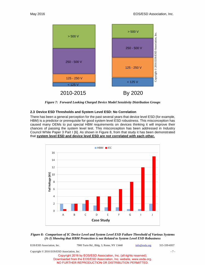
2.3 Device ESD Thresholds and System Level ESD: No Correlation
There has been a general perception for the past several years that device level ESD (for example, HBM) is a predictor or prerequisite for good system level ESD robustness. This misconception has caused many OEMs to put special HBM requirements on devices thinking it will improve their chances of passing the system level test. This misconception has been addressed in Industry Council White Paper 3 Part I [6]. As shown in Figure 8, from that study it has been demonstrated that system level ESD and device level ESD are not correlated with each other.
Figure 8: Comparison of IC Device Level and System Level ESD Failure Threshold of Various Systems
(A-J) Showing that HBM Protection is not Related to System Level ESD Robustness
2010-2015 By 2020
< 125 V
125 - 250 V
250 - 500 V
> 500 V
> 500 V
250 - 500 V
125 - 250 V
< 125 V Cop
yri
gh
t ©
201
6 E
OS
/ES
D A
ssoci
atio
n,
Inc.
Copyright 2016 by EOS/ESD Association, Inc. (all rights reserved). Downloaded from the EOS/ESD Association, Inc. website, www.esda.org.
NO FURTHER REPRODUCTION OR DISTRIBUTION PERMITTED.

May 2016 EOS/ESD Association, Inc.
EOS/ESD Association, Inc. 7900 Turin Rd., Bldg. 3, Rome, NY 13440 [email protected] 315-339-6937
Copyright © 2016 EOS/ESD Association, Inc. - 8 -
In reality, at the system level, ESD robustness is a much more complex issue requiring a deeper understanding to address the ESD protection requirements for electronic systems such as laptops, cell phones, printers and home computers. These system complexities come about as a result of protecting the external interfaces, such as the universal serial bus (USB), to the outside world. Such systems, after encountering the more severe ESD pulses such as those specified by the IEC 61000-4-2 [7] or ISO10605 [8] test methods, can lead to hard or soft failures. As introduced in White Paper 3 Part I, a co-design approach is required. A basic version of this (called system-efficient ESD design (SEED)) has been proposed which addresses hard failures related to IC pins with a direct external interface. For soft (reversible) failures, which are more frequently reported, more advanced co-design approaches are needed. These are more challenging to understand and overcome and require an extension of the SEED approach to other failure mechanisms that include latch-up and electromagnetic interference (EMI) effects. These challenges and approaches are discussed in Part II of White Paper 3 [9]. The important point for the present discussion is that none of these system level failures are improved or reduced by increased HBM or CDM device threshold levels. Thus, the technology scaling effects for both HBM and CDM as shown in Figures 2 and 6 would not have implications for system level ESD.
2.4 Process Control
ESD control programs have been in place for many years. One of the earliest programs involved the production of gunpowder. This simple program effectively kept the powder wet during manufacturing and handling. This kept the static charge low enough that the gunpowder would not ignite.
In the 1950’s and 1960’s, electronics were relatively insensitive to ESD events. The devices of the time could withstand most events without a problem. Even if they did fail for ESD events, the failures were a very small portion of the overall failure rates.
In the late 1970’s, with the introduction of large scale integration (LSI), ESD became a significant problem. A group of industry experts realized this and organized the first US ESD Symposium in 1978. At the time, technical papers were exchanged and there were workshops on problems and solutions. Companies at this time also started to implement ESD control programs. Each company had their unique program and did not share the information. The need for standardized programs was not recognized at that time.
The US Military was one of the first organizations to recognize the problems with static electricity and ESD. The first standard to address ESD process control was Mil-STD-1686 released in May of 1980. This standard, along with its companion handbook Mil-HBK-263, represented the first ESD control standard in the industry. All of the suppliers of electronics to the military were required to comply with this standard. However, most of the private sector still followed company developed procedures.
These early standards were focused on people and packaging. Controls in place for insulators were left mostly to the end user without much consideration except for the removal of non-required insulators. Tools, machines and automated equipment were not addressed or really considered as most of the processes were manual. The basic instructions were to keep everything and everyone handling the devices at the same potential.
An additional issue with these first ESD control programs was that the materials that were used to control static electricity did not have standards to qualify the materials. This led to many different types of testing, different methods and different instrumentation that caused different results. In some cases, materials measured by these methods did not perform well in controlling static. In the early 1980’s, a technical association, the ESD Association (ESDA) was formed to try and resolve some of the issues surrounding material testing. The first standards from the ESDA were simple material tests for items such as wrist straps, work surfaces and flooring. The standards did create a way to compare one product with another product. Suppliers of these materials were able to use the standards to improve their products. For example, the simple wrist strap has gone through many changes in the industry. What started out as a simple metal bead band has evolved into a system that makes better contact with a person and in some cases allows for continuous monitoring. Wrist straps provide a much more reliable connection than before and last longer. The
Copyright 2016 by EOS/ESD Association, Inc. (all rights reserved). Downloaded from the EOS/ESD Association, Inc. website, www.esda.org.
NO FURTHER REPRODUCTION OR DISTRIBUTION PERMITTED.

May 2016 EOS/ESD Association, Inc.
EOS/ESD Association, Inc. 7900 Turin Rd., Bldg. 3, Rome, NY 13440 [email protected] 315-339-6937
Copyright © 2016 EOS/ESD Association, Inc. - 9 -
standards also provide a way to test the wrist straps in a consistent manner so that a wrist strap that becomes defective can be removed and replaced. Before this, materials were used until they were physically damaged without regard to the electrical properties.
In the 1980’s and 1990’s the electronics manufacturing industry changed from each company having all the manufacturing reside within the company to a model that included many contract manufactures (CM) or electronic manufacturing suppliers (EMS). The military standard and the European standard, CECC 00 015:1991, became out of date. They were either too restrictive or did not address all aspects of a control program.
In 1995, the ESDA was given the task of replacing Mil-Std-1686 with an industry standard. The standard, ANSI/ESD S20.20-1999, was the replacement for ESD process control. Following this standard, a third party certification program was established to demonstrate compliance to the standard and has been very successfully applied to factory certifications all around the word, as shown in Figure 9. Today, this standard has been updated and replaced by ANSI/ESD S20.20-2014 [2]. In parallel, the IEC is updating IEC 61340-5-1 [3] to become technically equivalent to ANSI/ESD S20.20-2014. Both of these updates will improve control of materials and ESD control processes.
Figure 9: ANSI/ESD S20.20 Certificates Issued Since Inception
2.5 Process Capability Assessment
These ESD sensitivity trends will have a major impact on manufacturing process yields over the coming years. Companies will need to increase their efforts to verify that the installed ESD processes are capable of handling these devices and to make any necessary improvements in ESD control methods. This could include changes in the ESD control item limits, change in the frequency of compliance verification, and other forms of ESD monitoring, such as ESD event detection.
Formal means for establishing a quantitative process capability assessment have not existed until now. Through the efforts of ESDA Working Group (WG) 17 on process assessment, the ESDA has now released a technical report, ESD TR17.0-01-15 [10] with guidelines for how to establish a quantitative process capability assessment. An example of how to relate a control process (voltage on personnel) and device sensitivities is included in the HBM discussion below. A full process capability assessment, as discussed in ESD TR17.0-01-15, would have to take into account all control strategies.
Copyright © 2016 EOS/ESD Association, Inc.
Copyright 2016 by EOS/ESD Association, Inc. (all rights reserved). Downloaded from the EOS/ESD Association, Inc. website, www.esda.org.
NO FURTHER REPRODUCTION OR DISTRIBUTION PERMITTED.

May 2016 EOS/ESD Association, Inc.
EOS/ESD Association, Inc. 7900 Turin Rd., Bldg. 3, Rome, NY 13440 [email protected] 315-339-6937
Copyright © 2016 EOS/ESD Association, Inc. - 10 -
2.5.1 Human Body Model (HBM)
It has been shown that the resistance of a person to ground has a direct correlation to the maximum voltage on a person. Tests have shown that a resistance of 40 x 106 ohms or less is necessary to limit body voltage to less than 100 volts. Figure 10 shows the relationship between body voltage and resistance to ground. The limit for wrist straps provided within ANSI/ESD S20.20 is 35 x 106 ohms, which is approximately a 10% safety margin.
Voltage on Personnel
0
10
20
30
40
50
60
70
80
90
100
0 10 20 30 40
Resistance to ground (megohms)
Volts
Figure 10: Relationship Between Body Voltage and Resistance to Ground
For an ESD control program that uses ESD footwear and flooring to ground personnel, the situation is more complex. As people walk across an ESD floor while wearing ESD footwear, it is difficult to predict the voltage on a persons’ body due to the constantly changing body capacitance and the continuous charging and discharging of the person.
ANSI/ESD STM97.2 [11] can be used to determine the process capability of the footwear flooring system. An example of the type of information provided can be seen in Figure 11.
Figure 11: Determining Process Capability of a Footwear/Flooring System using ANSI/ESD STM97.2
Bo
dy V
oltage (V
)
Average of Maximum Peaks
3 Sigma
3 Sigma
3 Sigma
3 Sigma
Average of Minimum Peaks
Time (sec)
Copyright © 2016 EOS/ESD Association, Inc.
Copyright © 2016 EOS/ESD Association, Inc.
Copyright 2016 by EOS/ESD Association, Inc. (all rights reserved). Downloaded from the EOS/ESD Association, Inc. website, www.esda.org.
NO FURTHER REPRODUCTION OR DISTRIBUTION PERMITTED.

May 2016 EOS/ESD Association, Inc.
EOS/ESD Association, Inc. 7900 Turin Rd., Bldg. 3, Rome, NY 13440 [email protected] 315-339-6937
Copyright © 2016 EOS/ESD Association, Inc. - 11 -
2.5.2 Machine Discharge Events
Machine discharges occur when charged conductive surfaces come into contact with ESD sensitive devices. To minimize machine discharges, ensure that all conductive surfaces that come into contact or close proximity with ESD sensitive devices are grounded. If it is not possible to ground conductive surfaces, then measurements should be made to ensure that moving parts remain below a threshold voltage throughout the process. In ANSI/ESD S20.20-2014, the threshold is defined at 35 volts. Caution: this threshold level does not translate into any measured characterization with an MM tester. These measurements must be taken with the proper equipment, such as a contacting voltmeter or non-contacting voltmeter. Most field meters cannot make this measurement.
2.5.3 Events from Charged Devices and Static (Field) Induction (CDM)
In its pure form, a CDM event occurs when a charged ESD sensitive device is grounded or when a neutral device is grounded in the presence of an electrostatic field. The essential, unique characteristic of these events is that they involve a very fast rise time event between a device pin and another conductor at a different potential. CDM is the most relevant discharge model when single ICs are handled with automated equipment or manually by using hand tools. Thus, the CDM test method also gives an indication of the more general cases of conductor-conductor discharges such as touching a device lead with conductive tweezers. This includes many of the isolated conductor discharge events mentioned in the previous section.
Effective ESD control programs ensure that process required insulators will not induce a voltage onto the devices (static induction) being handled or that devices be tribo-electrically charged which could result in a damaging discharge of the device. As CDM thresholds are lowered, it becomes more difficult to depend on voltage control alone to provide adequate protection of devices. Thus, it is becoming more important to eliminate conductor-conductor contact wherever possible and use dissipative materials to avoid hard grounding.
2.5.4 Charged Board Events (CBE)
ICs and other ESD sensitive devices remain at risk when they are mounted onto printed-circuit boards and other assemblies. In fact, there is evidence that many ESD failures in circuit and system assemblies occur at the board level. These types of failures are referred to as charged board events (CBE). Most ESD testing and characterization of devices is done on stand-alone parts. This is the type of data that is summarized in the HBM and CDM roadmaps above. Further, IC failure analysis data, which is based on knowledge of failure signatures seen in standard HBM and CDM tests, has caused many to conclude that ESD failures are relatively rare when compared to other electrical failures commonly classified as electrical overstress (EOS). Recent data and experience reported by several companies and laboratories now suggest that many failures previously classified as EOS may instead be the result of ESD failures due to CBE (or cable discharge events [CDE] discussed in the next section). A charged board stores much more energy than a device because its capacitance is many times larger. In fact, the charge (energy) transferred in the event may be large enough to cause EOS-like failures to the devices on the board.
Current ESD control programs as implemented may not fully control charges on printed circuit boards and mechanics, thus, a CBE ESD risk may not always be fully controlled. Therefore, ESDA WG 25.0 will be issuing a technical report on CBE, and as knowledge of the CBE scenario increases, it will get higher consideration and scrutiny in failure analysis.
2.5.5 Cable Discharge Events (CDE)
The insulation on a communication cable (e.g., USB, Ethernet, etc.) is easily tribo-electrically charged by movement of the cable over surfaces such as desktops, floors, clothing, and work surfaces. This charging will in turn induce a potential on the conductors of the cable. When the charged cable is plugged into a system an ESD event occurs between a cable conductor(s) and one or more of the connector pins of the system receptacle depending on the connector design.
Copyright 2016 by EOS/ESD Association, Inc. (all rights reserved). Downloaded from the EOS/ESD Association, Inc. website, www.esda.org.
NO FURTHER REPRODUCTION OR DISTRIBUTION PERMITTED.

May 2016 EOS/ESD Association, Inc.
EOS/ESD Association, Inc. 7900 Turin Rd., Bldg. 3, Rome, NY 13440 [email protected] 315-339-6937
Copyright © 2016 EOS/ESD Association, Inc. - 12 -
This discharge is referred to as CDE. The resulting current pulse is highly dependent on the cable length and impedance. Industry reports indicate that CDE can cause an interface device to be damaged, create system “lock-up” or system upset. CDE is generally thought of as a charge equalization process between the victim unit or device and a charged cable, but a CDE can also occur if the victim unit (laptop, cellphone, etc.) becomes charged with respect to the cable. In the latter case, the victim unit becomes tribo-electrically charged via contact with some material or via a person being charged walking across a carpet, whether the cable is charged or the victim unit charged, the result is a discharge involving current flowing into or out of a cable.
3.0 TRENDS IN DEVICE LEVEL ESD TESTING
As described above, the decrease in ESD thresholds will put more pressure on the ESD control program to maintain high yields. In order to know where special procedures and scrutiny are required, one needs to know the device sensitivities. As pin counts increase and pin spacings decrease the evaluation of devices for their ESD thresholds has become more challenging. As a result, the HBM and CDM test methods have continued to change and additional changes are anticipated to track increasing device complexity. The increasing test costs and time continue to drive changes in these methods as well. In addition, other types of device level tests are under development to address stresses that occur beyond handling in the factory. These include the human-metal model (HMM) and transient latch-up (TLU). Use of transmission line pulsers continues to grow as a tool for up-front protection characterization. Another significant development has been the agreement by JEDEC, ESDA, and JEITA that the use of the method called “Machine Model” has been downgraded and is not recommended for use in device qualification.
3.1 Human Body Model (HBM)
In 2010, the ESDA and JEDEC HBM test methods were merged into a single document designated ANSI/ESDA/JEDEC JS-001-2010. Subsequent to this, the joint ESDA/JEDEC working group issued 2011, 2012, and 2014 [12] versions which implemented a number of changes.
The 2011 revision changed where (i.e., which pin combinations) the ESD stresses must be applied. These changes were driven by device technology evolution and by documented limitations of relay-based HBM simulators. In particular, changes were made to reduce device failures due to wear-out from excessive stresses (by hundreds or thousands) that were required by the previous version. A detailed discussion of these changes is available in the standard or the companion HBM User Guide, ESD JTR001-01-12 [13]. The new method changes the way an IO pin (non-supply pin) is HBM stressed to multiple supply pins. In the 2010 version of the standard, each IO pin is stressed to each independent supply pin. This pin combination has now been changed so that each IO pin is HBM stressed only to the supply pins that are directly associated with that IO pin. This change dramatically reduces the total number of stress pin combinations and significantly reduces the probability of generating HBM failures due to wear out failure mechanisms. This change was made because the HBM current paths used by the IO pins were found to be nearly identical to the ones used during the supply pin to supply pin tests.
Another change eliminated the IO to IO test pin combination for most pins, except for a small set of specialized coupled non-supply pins. The focused testing of IO pairs that could be weakly protected can provide an improvement over testing IO pins to all other IO pins tied together.
An option for improving testing repeatability and reproducibility is the inclusion of pin combinations for two-pin HBM testers. These HBM simulators, which may test without the use of sockets or test fixture boards, avoid the device-tester parasitic interactions that can cause unintended failure modes when testing some devices.
The 2012 version added modifications which address (1) responses to the evolution of advanced device structures and processes and (2) clarification of means for identifying low parasitic (more accurate) testers.
1. Defining and taking advantage of low impedance interconnection structures. This change allowed the representation of a supply or ground group of pins to be represented by a single
Copyright 2016 by EOS/ESD Association, Inc. (all rights reserved). Downloaded from the EOS/ESD Association, Inc. website, www.esda.org.
NO FURTHER REPRODUCTION OR DISTRIBUTION PERMITTED.

May 2016 EOS/ESD Association, Inc.
EOS/ESD Association, Inc. 7900 Turin Rd., Bldg. 3, Rome, NY 13440 [email protected] 315-339-6937
Copyright © 2016 EOS/ESD Association, Inc. - 13 -
pin according to the conditions described. The concept of a low-impedance above-passivation layer (APL), sometimes also known as a Redistribution Layer (RDL) was introduced.
2. Verification of and Testing with Low-Parasitic Simulators. These changes add a test to determine when a tester has sufficiently low parasitics to allow the elimination of certain “pin reversal” two-pin combinations.
The 2014 version introduced a sampling method for “cloned” non-supply pins. This new procedure is applied to a special set of identical IO pins called cloned IO pins. These sets can contain 100s of pins and stressing all of them is highly redundant and wastes test time and resources. The new procedure defines a statistical test which, if passed, allows a set of cloned IO pins to be represented by 30 randomly selected pins. The procedure determines if the set of 30 pins can be used to represent the entire group of cloned IO pins with a confidence level of 99%. Another new concept that has been introduced is the HBM target specification limit (SPL). If any of the randomly selected cloned IO pins fail at or below 1.5X SPL, then the new test procedure cannot be used. A special Excel statistical program that may be downloaded from the ESDA web site is available to assist in the calculation.
The joint working group is considering a more advanced method of statistical sampling for a future revision. Even with the improvements implemented in the previous version of ANSI/ESDA/JEDEC JS-001, the number of stresses to which a device is exposed is still high compared to the real-world scenario in which a device typically sees only one zap. Also, it is required to have a detailed knowledge of the design of the device; e.g., associated non-supply pins have to be identified which is often rather difficult and requires design and ESD expertise. This information is not usually available to the personnel performing the qualification tests.
The proposed approach goes a radical new way. Instead of grouping pins into supply, ground, and non-supply pins, all pins are treated equally. Each pin is stressed once against one randomly selected other pin tied to ground, and each pin is tied once to tester ground and a randomly selected other pin is stressed against this pin. The test procedure is hence a true two-pin test which can be performed by a two-pin test system as well as by a relay matrix based test system. Obviously, the only information on a device which is required is the pin list and possibly no-connect pins if those should be excluded from stressing. Preliminary work on this approach has shown that the stress count reduction and hence the test time reduction can be up to 95 percent, depending on the complexity of the device.
Other changes being considered are the addition of a 50-volt threshold level and the re-definition of ESD threshold to better reflect relative risk.
3.2 Charged Device Model (CDM)
CDM is continuing to advance as the accepted real-world ESD model for device ESD events in automated IC handling and manufacturing around the world. CDM ESD must consider device process – IO pin technology, minimum device size – pin pitch achievable in test, and CDM metrology limitations in the consideration of CDM roadmap direction over the next five years.
3.2.1 Device Thresholds
A combination of integrated circuit process technology advances, increasing device size and complexity and increasing IO speed requirements all point to lower minimum charged device model withstand thresholds, especially for the high performance pins. Minimum device CDM pin thresholds just below 100 volts in 2015 are forecast to reduce to below 50 volts by 2020. These pins may only be present on a small fraction of the total number of pins in any one package.
3.2.2 Device Size / Pin Pitch
A second limiting factor to CDM testing is the minimum device size and pin or ball pitch (distance between pins / balls on a package type). Minimum device sizes in 2015 are on the order of 400 by 600 µm, and this is forecast to be smaller by 2020. Minimum pin pitch of 350 µm achievable by CDM testers in 2015 may be reduced to on-die pad pitch by 2020, making CDM test capability
Copyright 2016 by EOS/ESD Association, Inc. (all rights reserved). Downloaded from the EOS/ESD Association, Inc. website, www.esda.org.
NO FURTHER REPRODUCTION OR DISTRIBUTION PERMITTED.

May 2016 EOS/ESD Association, Inc.
EOS/ESD Association, Inc. 7900 Turin Rd., Bldg. 3, Rome, NY 13440 [email protected] 315-339-6937
Copyright © 2016 EOS/ESD Association, Inc. - 14 -
require the use of probe technology similar to probe automated test equipment (ATE) today for those die form products.
3.3.3 CDM Testing Methodology
Two types of CDM testing are in use today. The first type, field-induced CDM testing, is in use by over 90% of the industry today. A recent advance in field-induced CDM testing was the publication of a combined ESDA/JEDEC CDM standard (ANSI/ESDA/JEDEC JS-002-2014 [14]) in 2015. The adoption of this new standard by the IC industry will allow field-induced CDM testing to produce more accurate results to 125 volts over the next 1-2 years. The limitations of the field-induced method are the minimum device size and pin pitch physical limitation of the CDM test equipment (which leads to multiple pin discharges for very small pitches) as well as the environmental variation of the discharge spark which is dependent on device size and charge voltage.
The continued reduction in minimum CDM pin thresholds described above will limit the use of field-induced CDM for many devices. An alternative CDM testing method, contact CDM (CCDM) has been shown in early trials to achieve a more accurate discharge pulse, independent of humidity and not dependent on the varying characteristics of the discharge spark in the field-induced CDM event. Research in approximating the impedance of the field-induced discharge spark with a discharge impedance in the contact CDM metrology chain (through transmission line and relay switching) is in progress and is expected to yield more accurate CDM testing at the very low (50 volts) levels needed by 2020 for those devices needing it. In addition, a second alternative CDM test method still using a contact approach, cc-TLP, is being investigated. This approach has been around for a much longer time but has the limitation of not being able to completely match the discharge waveform. However, this method is being considered as a possible wafer level characterization technique which would give significant information on protection structures in advance of any packaging and could be used as a solid figure of merit at the wafer level to compare the ESD robustness of various protection structures. It is expected that contact CDM test technology will become a more attractive alternative to field-induced CDM testing over the next five years as contact CDM research leads to further standardization of contact CDM worldwide.
Additionally, as with HBM, a sampling method will be investigated to see if the same time and resource savings can be realized with no impact to the CDM threshold assessment.
3.3 Transmission Line Pulse (TLP)
Over the last several years, transmission line pulsers (TLP) have become common place for early characterization of ESD protection structures. ANSI/ESD STM5.5.1 [15] has been the basis for much of this work. The standard practice (ANSI/ESD SP5.5.2 [16]) for very fast TLP has been demonstrated to give repeatable results [17]. WG 5.5 has worked to combine these into a single standard test method (STM) document, which describes TLP methods in a general sense. In addition to the merging of the above two documents, the descriptions for hardware requirements, waveforms, failure evaluation, calibration etc. have been improved. The new combined version of ANSI/ESD STM5.5.1 is expected to be released in 2016.
The new ANSI/ESD STM5.5.1 focuses on quasi-static TLP. This means that measurements are made in the latter part of the pulse where most of the transients have subsided. While this can give some information about turn-on characteristics, it is still not a true “transient” type of characterization. The WG has formed a sub-team to define a proposal on how to address the characterization of the initial transient response.
There continues to be discussion on how the various forms of TLP (very fast (VF)-TLP, transient VF-TLP, long pulse TLP, and standard TLP) can be used to universally characterize structures for HBM, CDM and even HMM. These discussions may eventually lead to the release of user or application guides for TLP.
Copyright 2016 by EOS/ESD Association, Inc. (all rights reserved). Downloaded from the EOS/ESD Association, Inc. website, www.esda.org.
NO FURTHER REPRODUCTION OR DISTRIBUTION PERMITTED.

May 2016 EOS/ESD Association, Inc.
EOS/ESD Association, Inc. 7900 Turin Rd., Bldg. 3, Rome, NY 13440 [email protected] 315-339-6937
Copyright © 2016 EOS/ESD Association, Inc. - 15 -
3.4 Human Metal Model (HMM)
Human metal model is the name given to stress tests applied to a device, but whose expressed intention is to simulate the stress on that device when a system is ESD stressed, usually with the IEC 61000-4-2 waveform. The working assumption is that this test will give a useful indication of how the device will perform in a system level ESD test and therefore help predict the system level performance. The main incentive for undertaking this work is that many OEMs have assumed that such a connection could be made. Some OEMs require that device suppliers perform such tests. However, the device-system correlation has not been established. In fact, there is a considerable concern that no such correlation should be expected.
Even in the absence of this correlation, OEMs continue to press their suppliers for this data. Therefore, it was considered beneficial to at least provide a way to standardize the stressing of devices with a “system-level” stress source. ESDA WG 5.6 was formed to establish the reproducibility with emphasis on how to test devices to the most common system-level ESD stress test, IEC 61000-4-2. The workgroup is looking at “ESD guns” and “HMM pulsers”. The workgroup conducted an extensive round robin that failed to demonstrate that the test method, as documented in ANSI/ESD SP5.6-2009 [18], produces repeatable or reproducible results across multiple sites. The workgroup suspects that the existing waveform specification with its wide tolerance is the major reason for the wide variation across test sites. Alternately, the failure to produce repeatable or reproducible results could be a variation in how the measurements were performed.
Finding a repeatable method will need further work and any revisions will likely take quite some time. These revisions may include a realization that stressing devices with the IEC 61000-4-2 [19] waveform, especially from ESD guns, may not be possible in a repeatable and reproducible manner. In this case an alternative method would be needed to assess the robustness of devices to system type stresses. Such a method may involve a test method such as a transmission line pulse (TLP).
3.5 Transient Latch-Up (TLU)
Integrated circuits can contain latch-up sensitive structures (e.g., parasitic thyristors) which can cause reliability issues during operation. For this reason, most semiconductor devices have to be qualified with respect to their latch-up sensitivity. JEDEC JESD78 [20] is the most commonly used latch-up qualification standard. However, this test has a rather slow rise time and long trigger pulse which does not cover many latch-up events. It is well known that fast transients, such as ESD, can trigger latch-up more efficiently. In 2004, this fast trigger mechanism was partially addressed by the test method described in ANSI/ESD SP5.4-2004, which was reaffirmed in 2008, as ANSI/ESD SP5.4-2008. However, this method had three fundamental problems which prevented it from being widely used as a common qualification or characterization method. First, by definition, a standard practice defines a test procedure that “may or may not yield a test result…which may not be reproducible.” ANSI/ESD SP5.4-2008 has not been elevated to a standard test method (STM) since the reproducibility was never proven with a round robin experiment. Secondly, ANSI/ESD SP5.4-2008 defined a trigger which could be used to identify latch-up sensitive designs but does not really reflect a worst-case real-world threat. Third, ANSI/ESD SP5.4-2008 was defined for one piece of test equipment which is not readily available and could not test modern, complex, integrated circuits which require extensive setup signals to place them in a state which is appropriate for latch-up testing. Therefore, the applicability of ANSI/ESD SP5.4-2008 was limited to a small number of integrated circuits and could not be used as a common test method to identify latch-up sensitive devices with trigger pulses which can occur in today’s applications. Due to these fundamental problems, ESDA WG 5.4 on TLU decided to re-classify ANSI/ESD SP5.4-2008 as a technical report [21] and re-start the work on a TLU standard from scratch.
In accordance with the “static” JEDEC JESD78 latch-up standard, the working group defines transient latch-up as a state in which a low-impedance path, resulting from a transient overstress that triggers a parasitic thyristor structure or bipolar structure or combinations of both, persists at least temporarily after removal or cessation of the triggering condition. The rise time of the transient overstress causing TLU is faster than 5 µs. The work in WG 5.4 on TLU does not cover changes
Copyright 2016 by EOS/ESD Association, Inc. (all rights reserved). Downloaded from the EOS/ESD Association, Inc. website, www.esda.org.
NO FURTHER REPRODUCTION OR DISTRIBUTION PERMITTED.

May 2016 EOS/ESD Association, Inc.
EOS/ESD Association, Inc. 7900 Turin Rd., Bldg. 3, Rome, NY 13440 [email protected] 315-339-6937
Copyright © 2016 EOS/ESD Association, Inc. - 16 -
of functional states, even if those changes would result in a low-impedance path and increased power supply consumption.
In 2013, as a first step towards a new and more general TLU test method, WG 5.4 released a technical report (TR), ESD TR5.4-04-13 [22]. The TR summarizes the current knowledge on TLU and discusses real-world TLU examples. Overall, 18 examples of different business fields are described. This variety of examples clearly demonstrated that transient latch-up is a real-world threat and must be considered as a serious reliability issue. Since the release of the TR, even more real-world cases have been reported and recent surveys and discussions in the semiconductor industry show the strong demand for a latch-up qualification or at least characterization method which covers fast transients as they might occur in field applications.
In 2014, in order to address the industry’s demands, ESDA WG 5.4 started a new document (standard practice) on TLU which defines a universal TLU characterization methodology. The proposed TLU trigger pulses and the set-up can be modified rather simply to match the requirements and constraints in a specific application. The characterization methodology can be applied to a broad range of applications, from simple test structures and discrete semiconductor devices to complex integrated circuits as stand-alone devices or in systems. Essentially, all TLU events discussed in ESD TR5.4-04-13 [22] can be reproduced by the proposed characterization methodology. The setups required to model a real-world TLU event should be technically realizable within a reasonable time fame. An important building block of the document is the verification methodology of the TLU set-up which ensures a correct pulse delivery to the device-under-test as well as a sufficiently fast response of the power supply. ESDA WG 5.4 plans a release of a standard practice towards the end of 2016.
It must be emphasized that the TLU test methodology proposed in the standard practice is intended to be used as a characterization methodology only, in contrast to the static latch-up test JESD78 which is a mandatory device qualification test. The TLU methodology can be applied to pins which might be endangered by fast transients in the field to characterize the robustness of those pins. There are no robustness thresholds defined in the standard practice, the desired TLU immunity level depends solely on the relevant application.
When the new TLU standard practice is released, ESDA WG 5.4 will monitor whether that test methodology efficiently helps the industry avoid TLU problems and if it will be widely adopted in industry. It is intended to establish a close cooperation with the JEDEC JESD78 working group, as both standardization committees face very similar technical challenges. In the future, the relevance of TLU compared to purely “static” latch-up, according to JEDEC JESD78, will certainly increase. Therefore, a close link between the JEDEC JESD78 standard and the ESDA WG 5.4 TLU standard is desirable.
3.6 Cable Discharge Events (CDE)
The ESDA is preparing a standard practice (SP) document which will provide guidance to industry for testing against CDE threats. This document will incorporate a recommended test procedure and will also outline techniques for measuring real world CDE events. Experiments by the members of WG 14 have identified test waveforms which can be effective for determining the CDE immunity of a system. The recommended test pulses have been selected to include both the fast rise time and longer duration characteristics of observed CDE waveforms. The document is intended to be used to test systems for sensitivities to discharges from cables or charged objects connecting to cables; however, since both events can be considered to be equivalent, only discharges from the cable will be described in the document. A draft version of a CDE standard practice is expected for release in 2016. In the meantime many OEMs and IC suppliers are using customer specific simulations.
4.0 NOVEL TECHNOLOGY TRENDS
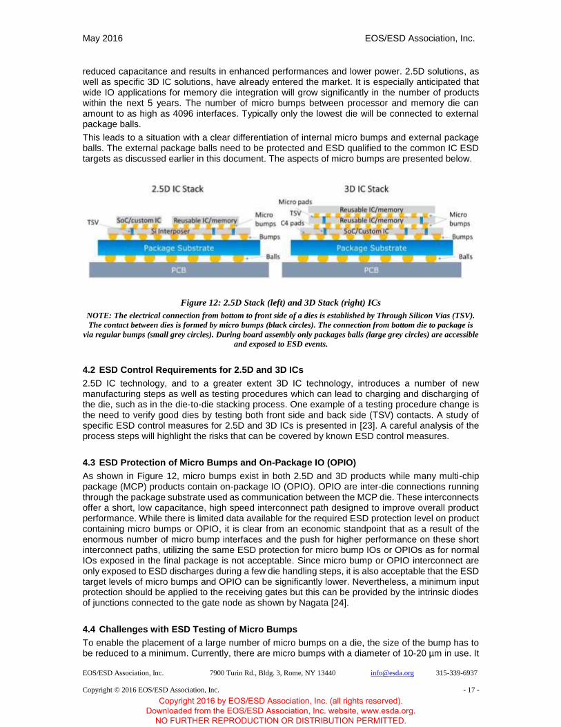
4.1 2.5D and 3D ICs
Novel die stacking processes are characterized by the use of through silicon vias (TSV) and the stacking of dies connected by micro bumps (see Figure 12). The motivation for use of these package techniques are a reduced foot print on the PCB and reduced wiring length which leads to
Copyright 2016 by EOS/ESD Association, Inc. (all rights reserved). Downloaded from the EOS/ESD Association, Inc. website, www.esda.org.
NO FURTHER REPRODUCTION OR DISTRIBUTION PERMITTED.
May 2016 EOS/ESD Association, Inc.
EOS/ESD Association, Inc. 7900 Turin Rd., Bldg. 3, Rome, NY 13440 [email protected] 315-339-6937
Copyright © 2016 EOS/ESD Association, Inc. - 17 -
reduced capacitance and results in enhanced performances and lower power. 2.5D solutions, as well as specific 3D IC solutions, have already entered the market. It is especially anticipated that wide IO applications for memory die integration will grow significantly in the number of products within the next 5 years. The number of micro bumps between processor and memory die can amount to as high as 4096 interfaces. Typically only the lowest die will be connected to external package balls.
This leads to a situation with a clear differentiation of internal micro bumps and external package balls. The external package balls need to be protected and ESD qualified to the common IC ESD targets as discussed earlier in this document. The aspects of micro bumps are presented below.
Figure 12: 2.5D Stack (left) and 3D Stack (right) ICs
NOTE: The electrical connection from bottom to front side of a dies is established by Through Silicon Vias (TSV).
The contact between dies is formed by micro bumps (black circles). The connection from bottom die to package is
via regular bumps (small grey circles). During board assembly only packages balls (large grey circles) are accessible
and exposed to ESD events.
4.2 ESD Control Requirements for 2.5D and 3D ICs
2.5D IC technology, and to a greater extent 3D IC technology, introduces a number of new manufacturing steps as well as testing procedures which can lead to charging and discharging of the die, such as in the die-to-die stacking process. One example of a testing procedure change is the need to verify good dies by testing both front side and back side (TSV) contacts. A study of specific ESD control measures for 2.5D and 3D ICs is presented in [23]. A careful analysis of the process steps will highlight the risks that can be covered by known ESD control measures.
4.3 ESD Protection of Micro Bumps and On-Package IO (OPIO)
As shown in Figure 12, micro bumps exist in both 2.5D and 3D products while many multi-chip package (MCP) products contain on-package IO (OPIO). OPIO are inter-die connections running through the package substrate used as communication between the MCP die. These interconnects offer a short, low capacitance, high speed interconnect path designed to improve overall product performance. While there is limited data available for the required ESD protection level on product containing micro bumps or OPIO, it is clear from an economic standpoint that as a result of the enormous number of micro bump interfaces and the push for higher performance on these short interconnect paths, utilizing the same ESD protection for micro bump IOs or OPIOs as for normal IOs exposed in the final package is not acceptable. Since micro bump or OPIO interconnect are only exposed to ESD discharges during a few die handling steps, it is also acceptable that the ESD target levels of micro bumps and OPIO can be significantly lower. Nevertheless, a minimum input protection should be applied to the receiving gates but this can be provided by the intrinsic diodes of junctions connected to the gate node as shown by Nagata [24].
4.4 Challenges with ESD Testing of Micro Bumps
To enable the placement of a large number of micro bumps on a die, the size of the bump has to be reduced to a minimum. Currently, there are micro bumps with a diameter of 10-20 µm in use. It
Copyright 2016 by EOS/ESD Association, Inc. (all rights reserved). Downloaded from the EOS/ESD Association, Inc. website, www.esda.org.
NO FURTHER REPRODUCTION OR DISTRIBUTION PERMITTED.

May 2016 EOS/ESD Association, Inc.
EOS/ESD Association, Inc. 7900 Turin Rd., Bldg. 3, Rome, NY 13440 [email protected] 315-339-6937
Copyright © 2016 EOS/ESD Association, Inc. - 18 -
is predicted that this feature size will scale down to a few µm over the years to come. Due to this, ESD stress testing, especially in CDM testing, of bumped dies will not be feasible. Assembly of the die in a reference package, where all micro bumps are routed to package bumps, leads to an unacceptable change in the actual CDM robustness. This is due to the need for a fan-out die for the micro bumps and the package parasitics, not to mention the huge effort and cost of building such a test chip IC. Since most wide IO interfaces are typically built up of a common ESD protection structure it is suggested to test representative IOs (like inputs, outputs, etc.) by forcing VF-TLP pulses with the use of microprobes. Alternatively, cc-TLP or wafer level TLP may be a future option to consider.
4.5 Target Levels
While the package bumps of 2.5D or 3D ICs need to satisfy regular ESD targets the micro bumps will follow a different specification. Since the likely characterization techniques discussed above are current testing methods, target values have to be specified in terms of current. Target peak currents for nanosecond pulses between 200 milliamperes and 1 ampere are discussed as being efficient and practical [23].
5.0 REFERENCES
[1] Industry Council on ESD Targets, White Paper 1: “A Case for Lowering Component Level HBM/MM ESD Specifications and Requirements,” August 2008, http://www.esda.org/white-papers.
[2] ANSI/ESD S20.20-2014, “Development of an Electrostatic Discharge Control Program for Protection of Electrical and Electronic Parts, Assemblies and Equipment”, July 2014 http://www.esda.org/standards/esda-documents.
[3] IEC 61340-5-1 “Electrostatics - Part 5-1: Protection of electronic devices from electrostatic phenomena - General requirements”, August 2007.
[4] JEDEC JESD 625B “Requirements for Handling Electrostatic-Discharge-Sensitive (ESDS) Devices”, January 2012 http://www.jedec.org.
[5] Industry Council on ESD Targets, White Paper 2: “A Case for Lowering Component Level CDM ESD Specifications and Requirements,” March 2009, http://www.esda.org/white-papers.
[6] Industry Council on ESD Targets, White Paper 3: System Level ESD, Part I: “Common Misconceptions and Recommended Basic Approaches”, December 2010 http://www.esda.org/white-papers.
[7] IEC 61000-4-2 “Electromagnetic Compatibility (EMC) – Part 4-2: Testing and measurement techniques – Electrostatic discharge immunity test”, 2008
[8] ISO 10605 – “Road vehicles – Test Methods for electrical disturbances from electrostatic discharge”, 2008, http://www.iso.org/iso/iso_catalogue.htm.
[9] Industry Council on ESD Targets, White Paper 3: System Level ESD, Part II: “Implementation of Effective ESD Robust Designs”, September 2012 http://www.esda.org/white-papers.
[10] ESD TR17.0-01-15, “For ESD Process Assessment Methodologies in Electronic Production Lines – Best Practices Used in the Industry”, January 2016 http://www.esda.org/standards/esda-documents.
[11] ANSI/ESD STM97.2-2006 “Floor Materials and Footwear – Voltage Measurement in Combination with a Person”, July 2006 http://www.esda.org/standards/esda-documents.
[12] ANSI/ESDA/JEDEC JS-001-2014 “Joint Standard for Electrostatic Discharge Sensitivity Testing – Human Body Model (HBM) – Component Level”, August 2014 http://www.esda.org/standards/esda-documents.
[13] ESD JTR001-01-12 “User guide of ANSI/ESDA/JEDEC JS-001 Human body Model Testing of Integrated Circuits”, 2012 http://www.esda.org/standards/esda-documents.
Copyright 2016 by EOS/ESD Association, Inc. (all rights reserved). Downloaded from the EOS/ESD Association, Inc. website, www.esda.org.
NO FURTHER REPRODUCTION OR DISTRIBUTION PERMITTED.

May 2016 EOS/ESD Association, Inc.
EOS/ESD Association, Inc. 7900 Turin Rd., Bldg. 3, Rome, NY 13440 [email protected] 315-339-6937
Copyright © 2016 EOS/ESD Association, Inc. - 19 -
[14] ANSI/ESDA/JEDEC JS-002-2014 “Joint Standard for Electrostatic Discharge Sensitivity Testing – Charged Device Model (CDM) – Device Level”, April 2015 http://www.esda.org/standards/esda-documents.
[15] ANSI/ESD STM5.5.1-2008 “Electrostatic Discharge Sensitivity Testing – Transmission Line Pulse (TLP) – Component Level”, May 2008 http://www.esda.org/standards/esda-documents.
[16] ANSI/ESD SP5.5.2-2007 “Electrostatic Discharge Sensitivity Testing – Very Fast Transmission Line Pulse (VF-TLP) – Component Level”, 2007.
[17] ESD TR5.5-03-14 “Very-Fast Transmission Line Pulse (TLP) Round Robin Analysis”, 2014 http://www.esda.org/standards/esda-documents.
[18] ANSI/ESD SP5.6-2009 “Human Metal Model (HMM) – Component Level”, January 2010 http://www.esda.org/standards/esda-documents.
[19] IEC 61000-4-2 “Electromagnetic compatibility (EMC) – Part 4-2: Testing and measurement techniques – Electrostatic discharge immunity test”, Ed. 2.0, 2008.
[20] JEDEC JESD78D “IC Latch-Up Test”, November 2011 http://www.jedec.org.
[21] ESD TR5.4-02-08 “Determination of CMOS Latch-Up Susceptibility – Transient Latch-Up - Technical Report No. 2”, 2008 http://www.esda.org/standards/esda-documents.
[22] ESD TR5.4-04-13 “Transient Latch-up Testing”, 2013 http://www.esda.org/standards/esda-documents.
[23] Global Semiconductor Alliance, “Electrostatic Discharge (ESD) in 3D-IC Packages”, Version 1.0, January 2015 http://www.gsaglobal.org/working-groups/3d-ic-packaging/.
[24] Nagata, M.; Takaya, S.; Ikeda, H.; Linten, D.; Scholz, M.; Chen, S.; Hasegawa, K.; Shintani, T. and Sawada, M. ‘CDM protection of a 3D TSV memory IC with a 100 GB/s Wide I/O data bus’, Proceedings EOS/ESD Symposium, 2014, p. 61 – 67.
Copyright 2016 by EOS/ESD Association, Inc. (all rights reserved). Downloaded from the EOS/ESD Association, Inc. website, www.esda.org.
NO FURTHER REPRODUCTION OR DISTRIBUTION PERMITTED.