electronics technology at · pdf filejohns hopkins apl technical digest, volume 24, number 1...
TRANSCRIPT
112 JOHNS HOPKINS APL TECHNICAL DIGEST, VOLUME 24, NUMBER 1 (2003)
A
Electronics Technology at APL
Harry K. Charles Jr.
PL programs have made signifi cant and continuous use of electronics technology from the very beginning. In fact, the VT fuze was a marvel of the Laboratory’s electron-ics technology and the ingenuity of its practitioners. Electronics technology at APL can be subdivided into fi ve broad areas: microelectronics and advanced packaging, RF and microwaves, embedded computers and programmable devices, microelectromechanical systems, and optoelectronics/photonics. In each area, a historical background is presented along with the status of current activities and the trends, directions, and challenges for evolution at the Laboratory. This information was compiled from the APL Senior Leadership Team Technology Review on Electronics Technology. The Laboratory has developed extensive and, in some cases, unique capabilities and facilities for electronics design, fabrication, testing, and qualifi cation. These assets exist in seven APL depart-ments and have been applied across all program areas. The article also highlights a few of the many electronics technology–intensive projects completed recently or currently under development.
INTRODUCTIONAPL has a long history of developing innovative
systems for national defense and space using electron-ics technology. In fact, the application of modern innovative electronics technology traces back to the very roots of the Laboratory with the development of the VT fuze.1 The VT fuze, viewed as one of the three most important inventions of the Second World War, was a marvel of modern electronic design and packaging at the time. Despite the simplicity of the circuitry (by today’s standards), it used state-of-the-art miniaturized tubes, which were developed by industry especially for the fuze application, and the latest in shock-mounting techniques (the VT fuze had to perform after being sub-jected to shock loads exceeding 20,000 g’s, i.e., 20,000
times the force of gravity). From this exciting beginning until today, the Laboratory’s electronics technology is an underlying enabling capability for our systems busi-ness. From radars to spacecraft and all major develop-ments in between, APL’s electronics technology has played a signifi cant role.
This article focuses on the fundamental building blocks of our electronics technology rather than on the system aspects. For example, in a radar system, we would focus on the transmit and receive (T/R) modules rather than the radar itself. Similarly, in a satellite, our attention would be on custom chips, circuit boards, and system-building elements such as antennas and com-mand and data communications systems.

JOHNS HOPKINS APL TECHNICAL DIGEST, VOLUME 24, NUMBER 1 (2003) 113
ELECTRONICS TECHNOLOGY AT APL
Because of this building block approach, we have divided APL’s electronics technology into fi ve areas: microelectronics and ad-vanced packaging, RF and micro-waves, embedded computers and programmable devices, microelec-tromechanical systems (MEMS), and optoelectronics/photonics. The essential content of these areas, along with their basic interrela-tionships, is shown in Fig. 1. As can be seen, the core of our electronics technology revolves around chips and electronic circuitry (analog and digital circuits for command, control, and data analysis) coupled with RF and microwave circuitry and subsystems for communication and, of course, radar applications. These critical core elements are linked through advanced packag-ing technology and the use of programmable functionality pres-ent in our embedded computers and programmable devices. MEMS and optoelectronics/photonics, al-though practiced at much lower levels of effort (5 to 10%) than the other technologies, can be disrup-tive2 for APL core electronics, and thus their future impact and the need for development lead time and investment must be taken into account. Figure 2 relates the fl ow and interplay of the fi ve electron-ics technology subareas in the APL systems development process.
Before we consider these fi ve subareas of the electron-ics technology taxonomy, it is necessary to trace some of the major events in history, both the Laboratory’s and the electronics industry’s, that have shaped our technology.
HISTORICAL BACKGROUNDThe key element in the Laboratory’s history, of
course, is its founding with the development of the VT fuze. Evolving from the VT fuze was APL’s role in the shipboard defensive missiles of the 1950s and early 1960s (Terrier, Talos, and Tarter),3 which has led to our role today with Standard Missile4 and Tomahawk.5 As we progressed with the shipboard defensive missiles, our electronics technology grew and evolved, combining the transistor and integrated circuits (ICs) with advances in guidance, navigation, and tracking. A particularly
APL core
ASICs, FPGAs,software
Analog and digitalelectronics
(programmable devices)
Microelectro-mechanical
systems (MEMS)Sensors, actuators,
structures,systems
Electronics Technology
Microelectronicsand advanced
packagingICs, components,
substrates,interconnections
Antennas, poweramplifiers, oscillators,
receivers
RF andmicrowaves
Optoelectronicsand photonics
Lasers, detectors,modulators,lightguides
Figure 1. Relationships among the fi ve major sub-elements of APL’s electronics technology (ASICs = application-specifi c inte-grated circuits, FPGAs = fi eld-programmable gate arrays).
Figure 2. A detailed interpretation of how APL’s electronics technology fl ows into the Laboratory’s end-use system applications (COB = chip on board, DCA = direct chip attach).
important element has been the development of the printed wiring board (PWB), along with other advanced substrates.
APL’s entry into space, with its leading role in satellite navigation, had a profound effect on our electronics technology. Miniaturized high-reliabil-ity packaging at the Laboratory was reinvigorated with the dawning of the Space Age. The need to pack more and more electronic functionality into a small, lightweight structure forced APL and others to develop innova-tive methods for packaging, ranging from the ministick6 of the 1960s to our chip-on-board efforts of the late 1990s. This ongoing need for high-density, highly functional electronics in each satellite or instrument forced APL space electronics to use advances in custom chips, programmable devices, and of course the fi eld programmable gate array (FPGA).
The Laboratory has been an innovator in space electronics, including being the fi rst to use the microprocessor in space.7 Because of the weight of
DCACO
B
End-useapplications
Semiconductors(Si, GaAs, SiC)
Chips/ICs(digital, analog, mixed;
RF and microwave;MEMS; optoelectronics
and photonics)Electronic,
MEMS, and opticalpackaging
Softwaredevelopment
Mechanical/optical parts(non-MEMS)
Printedwiring boards
(other substrates)
Board-levelassembly, test(programming)
Package-level test
(programming)
Embedded softwaredevelopment and
programming
Subsystemassembly, test(programming)
Systemintegration, test(programming)
Single-chippackaging
Multichippackaging
Electronic,mechanical,
optical systemdesign
114 JOHNS HOPKINS APL TECHNICAL DIGEST, VOLUME 24, NUMBER 1 (2003)
H. K. CHARLES JR.
spacecraft and their limited power, APL has also had to make advances in communications equipment. Our impressive history in this area ranges from the develop-ment of solid-state transmitters and receivers to anten-nas, which have evolved from the bifi lar applications of the 1970s to today’s infl atable parabolic dish. Likewise, our work in phased array radar has evolved from simple, low element structures to the huge, complex phased array radar systems that form the heart of APL’s Coop-erative Engagement Capability.8
MICROELECTRONICS AND ADVANCED PACKAGING
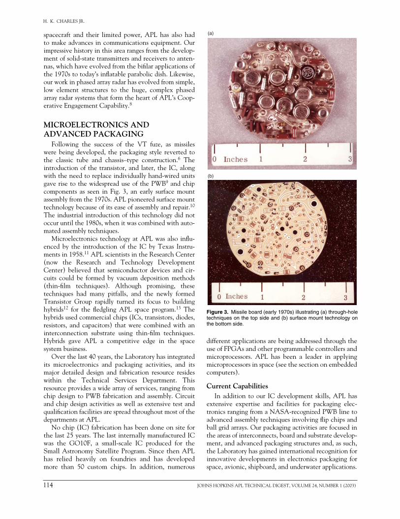
Following the success of the VT fuze, as missiles were being developed, the packaging style reverted to the classic tube and chassis–type construction.6 The introduction of the transistor, and later, the IC, along with the need to replace individually hand-wired units gave rise to the widespread use of the PWB9 and chip components as seen in Fig. 3, an early surface mount assembly from the 1970s. APL pioneered surface mount technology because of its ease of assembly and repair.10 The industrial introduction of this technology did not occur until the 1980s, when it was combined with auto-mated assembly techniques.
Microelectronics technology at APL was also infl u-enced by the introduction of the IC by Texas Instru-ments in 1958.11 APL scientists in the Research Center (now the Research and Technology Development Center) believed that semiconductor devices and cir-cuits could be formed by vacuum deposition methods (thin-fi lm techniques). Although promising, these techniques had many pitfalls, and the newly formed Transistor Group rapidly turned its focus to building hybrids12 for the fl edgling APL space program.13 The hybrids used commercial chips (ICs, transistors, diodes, resistors, and capacitors) that were combined with an interconnection substrate using thin-fi lm techniques. Hybrids gave APL a competitive edge in the space system business.
Over the last 40 years, the Laboratory has integrated its microelectronics and packaging activities, and its major detailed design and fabrication resource resides within the Technical Services Department. This resource provides a wide array of services, ranging from chip design to PWB fabrication and assembly. Circuit and chip design activities as well as extensive test and qualifi cation facilities are spread throughout most of the departments at APL.
No chip (IC) fabrication has been done on site for the last 25 years. The last internally manufactured IC was the GO10F, a small-scale IC produced for the Small Astronomy Satellite Program. Since then APL has relied heavily on foundries and has developed more than 50 custom chips. In addition, numerous
Figure 3. Missile board (early 1970s) illustrating (a) through-hole techniques on the top side and (b) surface mount technology on the bottom side.
(a)
(b)
different applications are being addressed through the use of FPGAs and other programmable controllers and microprocessors. APL has been a leader in applying microprocessors in space (see the section on embedded computers).
Current CapabilitiesIn addition to our IC development skills, APL has
extensive expertise and facilities for packaging elec-tronics ranging from a NASA-recognized PWB line to advanced assembly techniques involving fl ip chips and ball grid arrays. Our packaging activities are focused in the areas of interconnects, board and substrate develop-ment, and advanced packaging structures and, as such, the Laboratory has gained international recognition for innovative developments in electronics packaging for space, avionic, shipboard, and underwater applications.

JOHNS HOPKINS APL TECHNICAL DIGEST, VOLUME 24, NUMBER 1 (2003) 115
ELECTRONICS TECHNOLOGY AT APL
Our wirebond interconnection program has been carried out for many years and has evolved to a mature, highly effi cient, highly reliable operation. New fl ip chipping capabilities have been added, with emphasis on fl exible bumps for cryogenic applications (space radiation detectors, cooled high-speed digital circuitry). Multichip packaging at APL can take many forms. The three primary forms are (1) chips placed on a multi-layer thin-fi lm circuit board with a wirebonded or fl ip chip interconnect, (2) chips incorporated on ceramic substrates (either thick fi lm or ceramic cofi red14), and (3) chips directly mounted on fi ne-line PWBs using either wirebonding or fl ip chipping techniques. Such direct mounting of chips on PWBs is called “chip-on-board”14 and has been used by the Space Department in several advanced development activities.7
Board-level assembly is typically a combination of surface mounting and through-hole technologies, with some automated part placement and machine soldering. NASA-certifi ed hand soldering forms the bulk of our electronic component interconnect activities.
StrengthsThe Laboratory has much strength in the areas of
microelectronics and advanced packaging, including
In wirebonding, we have international recognition for our wirebonding studies program. In fl ip chip solder-ing, we have a proprietary indium bumping process that allows delicate detector chips to be attached. The process is suitable for use with all chips operating at cryogenic temperatures.
As mentioned, another strength in the microelec-tronics arena is our ability to design custom chips. Once designed, interfaces exist for commercial foundries as well as for using the MOSIS network15 because of our University affi liation. Radiation-hardened custom work has also been done with Sandia National Laboratory and Harris Semiconductor.
Future Directions and OpportunitiesWhile APL has excellent microelectronics and
advanced packaging capabilities, continued focus on enhancing technical expertise and gaining access to adequate resources must be maintained. Future success depends on the ability to select from the myriad tech-nologies available for advanced packaging and micro-electronics in general and then to put the necessary equipment and development processes in place to make them viable entities for meeting the needs of future
(a)
(b)
Figure 4. Modern circuit board technologies developed at APL: (a) multilayer proces-sor boards used on the Near Earth Asteroid Rendezvous (NEAR) Shoemaker and the Advanced Composition Explorer (ACE) satellites and (b) rigid fl ex board for the NEAR Infrared Spectrograph.
a government-certifi ed PWB line. This facility not only supplies boards to our APL customers but also is sought by sponsors (e.g., NASA/Goddard Space Flight Center) to do their most demanding work. In addi-tion, the PWB line turns out preci-sion organic boards with blind and buried vias for use with our chip-on-board technology. Key to this process is autocatalytic gold plating, which allows reliable wirebonding to the board’s copper metallization. The PWB line produces about 1000 boards a year of approximately 100 different designs and is certifi ed for multilayer polyimide boards as well as rigid fl ex boards (Fig. 4). In addi-tion to organic-based PWBs, APL also has capabilities to manufacture circuit boards using print and fi re technologies (thick fi lm and low-temperature cofi red) on ceramic and multilayer thin fi lm on silicon (with polyimide as the dielectric).
Another APL strength is our advanced assembly processes for both bare chips and packaged parts. These methods include wire-bonding, fl ip chip soldering, and solder refl ow for packaged parts.

116 JOHNS HOPKINS APL TECHNICAL DIGEST, VOLUME 24, NUMBER 1 (2003)
H. K. CHARLES JR.
APL customers. Strategic planning, as well as practi-cal implementation plans, will need to be developed to allow us to navigate swiftly and accurately through the growing maze of the microelectronics and advanced packaging fi elds.
Particular attention must be paid to miniature solder ball interconnect such as those found in fl ip chipping and chip-scale packaging (microball grid arrays). In particular, we must bring our knowledge of fabrication, quality assurance, and long-term reliability to the same level of maturity and recognition achieved by our wire-bonding activities. Fortunately, APL has established an excellent base upon which to build this required knowledge in miniaturized soldering. Extensive work with leadless chip carriers during the 1980s provided signifi cant insights into the soldering process and the mechanisms of failure. Fundamental studies of fatigue16 have led to new methods of analyzing and predicting solder failures as well as a generalized appreciation of solder joint reliability.17
Another need is developing advanced substrates that can support the ever-increasing chip functional-ity produced by the IC revolution as manifested by Moore’s law.18 This requirement will put the surface real estate of circuit boards at a premium, forcing other circuit elements (e.g., resistors, capacitors, and inductors) off the top (and bottom) surface and into intervening substrate layers. Such buried components are typically called embedded passives. Achieving the required accuracy and reliability necessary for stringent APL applications poses a challenge to current embed-ded passive technology.
We also must ensure that our wirebonding expertise is maintained as chip metallizations change from alumi-num alloys to copper. Reliable bonding to copper is pos-sible, and preliminary work at APL suggests that it can be brought online in the next few years, provided continued effort is applied.
RF AND MICROWAVESAPL has a rich history of ac-complishments in the
RF and microwave arenas, ranging from the one-tube transmitter that was the heart of the VT fuze to the large phased array radar systems that are part of the Cooperative Engagement Capability. The Laboratory has been a leader in the development of phased array radar systems (antennas, T/R modules, etc.) from its beginning.19 Our early efforts were at S band with small, 256-element antennas. Our latest units are at X band and above in frequency, with systems containing thousands of elements. Initial work on digital beam-forming radar has begun.
Monitoring the Doppler shift of radio signals from Sputnik allowed APL pioneers Weiffenbach, Guier, and McClure to prove that you could determine a
satellite’s precise orbit if you knew your precise location on Earth.20 These inventors then reasoned, by turning the equations around, that if you knew the satellite’s current position and could predict its orbit, you could use the Doppler shift to locate a receiver on Earth. Thus began the era of satellite navigation, and the Transit Satellite Navigation System was born, with its myriad RF innovations ranging from antennas and command receivers to the world’s most stable oscillator for space applications.
Current CapabilitiesRF and microwave applications are being developed
in several departments at the Laboratory. The major activities, however, are located in the Air Defense Systems Department (ADSD) and the Space Depart-ment (SD). ADSD activities primarily focus on radar detection and tracking schemes for aircraft and mis-siles. Other capabilities for the development of seek-ers, receivers, and missile communications systems exist. Extensive test and development facilities for key electronic components such as T/R modules are available to facilitate phased array radar system development.
RF and microwave design and development capa-bilities for application in space reside primarily in SD. These capabilities include engineering workstations for design, extensive fabrication facilities (much of it located in the Technical Services Department), and a full array of electronic test equipment that can analyze system performance over the frequency spectrum from DC to above 100 GHz. Antenna design is done in both ASDS and SD, and physical test facilities include anechoic test chambers and an antenna range complete with its own boresighting capability.
Satellite navigation activities continue today with a strong Global Positioning System (GPS) capabil-ity located in several departments. APL has applied GPS in many system applications ranging from missile tracking and guidance to the tracking of gun-launched munitions.
StrengthsAPL strengths in the RF and microwave arenas
are signifi cant. Key development and test capabilities exist for T/R modules. Current modules use GaAs chip technology with a variety of high thermal conductivity substrates including Al2O3, AlN, silicon, and silicon carbide. The use of diamond as a substrate and heat spreader has been explored. SiC transistors that can have operating temperatures above 900°C have been investigated, and preliminary tests have been per-formed. Microwave circuit packaging is an important strength for the Laboratory since all package elements are essential to determining the ultimate performance of

JOHNS HOPKINS APL TECHNICAL DIGEST, VOLUME 24, NUMBER 1 (2003) 117
ELECTRONICS TECHNOLOGY AT APL
the microwave circuit. Particularly important elements are APL’s ability to produce precision, patterned circuit patterns on the substrates and to make controlled shape and length wirebonds.14 Precise, repeatable wirebonds allow high-performance, high-frequency circuits to be reliably fabricated.
Antenna technology is another major element of APL’s RF and microwave base. We are strong in the development of planar phased arrays for shipboard and airborne radar applications as well as high-performance communications antennas for use in space. Several APL-developed antennas were space fi rsts, including quadrifi lar and bifi lar helix antennas. The current hybrid infl atable antenna (Fig. 5) has important impli-cations for existing and future spacecraft. Unlike previ-ous infl atable antennas, which were practically useless if they failed to infl ate, our hybrid antenna has a central, rigid dish that can still provide vital communications links even if the infl atable portion fails to deploy. Although the gain would be reduced, important com-mand, control, and scientifi c information could still be transmitted or received.
Another important strength is APL’s extensive expe-rience in the design and development of precision oscil-lators. We build the world’s most stable fl yable oscil-lators. Over 400 units have been built to date. These 5-MHz oscillators (Fig. 6) allow precision timing and serve as a reference standard for all types of coherent communications and signal processing systems. When combined with frequency distribution units, they can provide ultrastable reference signals at frequencies up to 1 GHz. The oscillator units have signals with excel-lent short-term frequency stability, typically better than 5 � 10–13 over a 1-s period, and have been so successful that APL technology has been spun off in a commercial venture called Syntonics.21
Future Directions and OpportunitiesThe Laboratory’s microwave and RF technologies are
at a transition point. Analog phased array beamforming is giving way to all-digital beams. The need to develop multiple digital beam phased array radar systems is an important challenge for us. Handling multiple digital beams simultaneously will require new test and mea-surement capabilities along with training of APL staff in digital beamforming science. Key technical skills and resources will be necessary to bring these design, devel-opment, and test capabilities online.
In the arena of space communications, the need to move higher in frequency is paramount. As the Labora-tory embarks on planetary and interplanetary missions, signals take longer to reach the Earth. The NEAR mis-sion alone experienced one-way signal delays of almost 18 min when it landed on the asteroid Eros. Higher frequency affords higher bandwidth, which is neces-sary to cram the most information into these delayed signals. Today, our dominant space communication fre-quencies are at C band. The future will see a migration to Ka band.
The center frequency of the 5-MHz oscillator must also be moved upward. Studies have shown that the frequency must be greater than 500 MHz to achieve the size, noise, and stability requirements for an advanced oscillator. The current oscillator/frequency distribution unit occupies approximately 1000 cm3, including power supply, whereas an advanced oscillator could occupy a volume of less than 60 cm3.
EMBEDDED COMPUTERS AND PROGRAMMABLE DEVICES
Our embedded computers and programmable devices, along with microcontrollers, are at the heart of most
Figure 5. Hybrid infl atable antenna developed by APL’s Space Department. The rigid dish in the center is 0.5 m in diameter; the entire antenna infl ates to an overall diameter of 2 m.
Figure 6. Internal view of APL’s ultrastable quartz oscillator assembly. The precision quartz crystal and APL’s proprietary dual heater oven are contained within the cylindrical fl ask in the lower front of the photograph.

118 JOHNS HOPKINS APL TECHNICAL DIGEST, VOLUME 24, NUMBER 1 (2003)
H. K. CHARLES JR.
electronic subsystems and systems developed at the Laboratory today. These resources build on a long his-tory of innovation in electronics and signal processing. Such developments range from the custom multitasking controller for the robotic prosthetic arm developed for the Veterans Administration in 1976 to the current extensive use of FPGAs and general-purpose micropro-cessor chips in the latest spacecraft.
Many fi rsts in this arena have occurred at the Labo-ratory.22 For example, the fi rst microprocessor (Intel 8080) in space was fl own by APL in the SEASAT-A program in 1978, MAGSAT saw the fi rst use of a radia-tion-hardened RCA 1802 microprocessor in space in 1982, and the Hopkins Ultraviolet Telescope used a bit slice microprocessor (Advanced Micro Devices 2903) that was microprogrammed to execute a Forth language kernel.23 A custom Forth Reduced Instruction Set Chip (FRISC) was designed at APL in 1985. The FRISC chip was a 32-bit native Forth language processor, and the design has been commercialized.
Recent custom chip developments include the digi-tal multibeam steering (DIMUS) acoustic beamforming chip (Fig. 7) developed to improve sonar system opera-tion. The DIMUS chip, when combined with nine other DIMUS chips, forms a custom sonar array beamforming system that processes signals from 960 hydrophones simultaneously. Development of these chips reduced the sonar system’s size by a factor of 50 or greater.
Figure 8 is a photograph of the TRIO chip, a custom sensor interface chip developed by APL. The design has been selected by the Jet Propulsion Laboratory for use in its future space programs. Similar developments are evident throughout the Laboratory in applications
ranging from missile guidance and underwater instru-mentation controllers to microprocessor-based systems for the operation of implantable biomedical devices such as the programmable implantable infusion pump.24
Current CapabilitiesCapabilities for the development of embedded
computers and programmable devices exist throughout the Laboratory. Considerable effort is expended in all departments on the design and programming of these devices and systems. Although APL has custom chip design capabilities, most of the effort is dedicated to the application of commercial devices. Programming and emulation tools are on hand for most microprocessor chips available today.
When a commercial device does not have the desired functionality, a custom device can be obtained through two routes. The fi rst route is the development of a full custom design using our extensive base of Mentor and University computer-aided engineering tools. The chips, once designed and simulated, can be fabricated via a commercial foundry or through the use of the Uni-versity-affi liated MOSIS network. APL has an excellent working relationship with several foundries that allows custom chips to be developed in both CMOS and bipo-lar technologies, including devices that are radiation hardened. The second route is the use of FPGAs, which use fusable links to provide custom interconnections between standard devices and building block elements already fabricated on an IC. This programming burns in a custom pattern of interconnects and hence circuitry to meet the design need. Although the FPGA manufac-turer has predetermined which devices and functional building blocks exist on a chip, it is possible to support a high percentage of custom needs using this technology. Unlike custom devices, the design and chip costs are
Ring randomaccess
memory
Ringcomputation
section
Decouplingcapacitors
121 lead pingrid array package
Figure 7. DIMUS IC chip custom designed at APL. The chip uses CMOS technology. It was designed with APL’s MAGIC, IRSIM, and ModelSim software and fabricated through the MOSIS net-work. The chip contains 2 million transistors and uses 0.8-µm design rules.
Figure 8. TRIO IC chip custom designed at APL. TRIO is an interface chip for use between sensors and the rest of the space-craft systems. It contains the buffering and other on-chip cir-cuitry to perform particularly well in temperature measurement applications.

JOHNS HOPKINS APL TECHNICAL DIGEST, VOLUME 24, NUMBER 1 (2003) 119
ELECTRONICS TECHNOLOGY AT APL
much lower and the development time is signifi cantly less (i.e., a few days compared to months or years). The Laboratory has several FPGA programming sta-tions staffed with trained personnel. These stations use FPGA design tools that are supported on the computer-aided engineering design network.
Moving more into the systems arena, APL is developing a single-chip GPS receiver that will be highly jam-resistant. Both the Adaptive Instrument Module (AIM) and the Adaptive Processing Template (ADAPT) are APL efforts to build reprogrammable hardware for space applications. In these programs, soft-ware instructions are used to change the architecture and functionality of the instrument module so that it can adapt to changes in sensor input, adapt to changes in the quality of the data, or perform a new function not anticipated prior to launch. AIM is schedule to fl y on the Australian Federation Satellite spacecraft; ADAPT is targeted for technology demonstration fl ights associ-ated with the Living With a Star Program.
StrengthsAPL strengths in embedded computers and program-
mable devices are signifi cant. Excellent test and simula-tion facilities for a large number of commercial chips and processors are located throughout the Laboratory. Many engineers have extensive experience in the design and development of computer hardware and software for embedded processors for a wide range of applications including space, underwater, and biomedicine. Other engineers are practiced in the development of Forth-based systems and the fl exibility to use the embedded system best suited for the application. The Laboratory has the ability to make the trade-offs between custom chips, FPGAs, and commercial chips for the given application to ensure a timely and cost-effective solu-tion for the given system specifi cations. In addition, APL has engineers skilled in the development of both analog and digital circuitry, including the development of expertise in analog FPGAs.
Future Directions and OpportunitiesThe state of the art is advancing at breakneck speed,
driven by Moore’s law and the demand for more com-puting power in all applications. As a result, analog FPGAs will be widely available and digital FPGAs will include analog subcells. The extensive use of simple digital serial interfaces such as the universal synchro-nous bus will propel the development of chip drivers and ultimately affect chip architecture. Current 8-bit microcontrollers will expand to 12- and 16-bit cores and are drifting toward 32-bit digital signal processor performance. Reprogrammable hardware, particularly with analog subcells, will be key to many future instru-ments. Software-driven reprogrammability with drop-in code in VHDL-type environments will enable these
cells to produce blocks capable of complex functions such as fast Fourier transforms.
APL must embrace these advances while maintain-ing a strong core of applications-related expertise. For example, the development of standard components for use in embedded projects should be encouraged. This would include components such as a modern proces-sor to replace the aging RTX2010 used by many space instruments and in other applications. The use of stan-dard interface chips and protocols such as PCI will need to be strongly emphasized. Embracing standards such as PCI, rather than always creating our own, will allow us to leverage commercial equipment and software analysis tools to test and debug our embedded computers and programmable devices and will give us more fl exibility in using components from many vendors.
MICROELECTROMECHANICAL SYSTEMS
MEMS devices are mechanical and electromechan-ical parts fabricated at micrometer scales using the design and processing methods associated with the IC industry.25 The acronym MEMS appeared during the 1980s, although the concept of three-dimensional pat-terning of silicon and other materials associated with the IC industry was known at least 20 years before the introduction of the term. MEMS devices consist of one or more mechanical elements (e.g., cantilevers, hinges, pivots, shutters, gears, etc.) that are free to move under externally applied forces or are made to move by inter-nally applied fi elds. The fi rst MEMS chip designed at APL was 5 mm � 5 mm and contained hundreds of cantilevers, doubly supported plates, and inter-digital structures.
These devices were fabricated using the Multi-User MEMS Processing System (MUMPS) foundry. An electron microscope photograph of a MEMS cantilever on APL’s fi rst MEMS chip is shown in Fig. 9. When
Figure 9. End-weighted MEMS cantilever on APL’s fi rst MEMS chip. The cantilever is suspended approximately 2 µm above the surface.
120 JOHNS HOPKINS APL TECHNICAL DIGEST, VOLUME 24, NUMBER 1 (2003)
H. K. CHARLES JR.
received, the cantilever was attached to the base by a 2-�m-thick sacrifi cial layer. The removal of the sacrifi -cial layer allows the movable mechanical element (e.g., cantilever, shutter, etc.) to be freed from the base layer. Because the mechanical elements are very fragile in a macro sense (they are very strong at the microscale), they are shipped from the MUMPS foundry with the sacrifi cial layers in place. Upon receipt, the sacrifi cial layers must be etched away to free the movable devices. Care must be exercised in both design and release pro-cessing to ensure that the freed mechanical elements are not damaged or lost in the release process.
Today, applications for MEMS devices range from simple mechanical parts used as sensors and actuators to full-blown systems combining extensive electronic control and signal processing right on the chip with the electromechanical parts. The effective integration of electronic circuitry on the same IC-sized chip con-taining the MEMS parts, together with the appropri-ate packaging, is a major challenge facing the MEMS world. Integrated systems combining active electronic devices with MEMS pressure sensors, accelerometers, and optical mirrors have already achieved commercial success. Devices such as chip-sized chromatography sys-tems, fl uid pumping systems, and microphone amplifi er systems will soon penetrate the marketplace.
In addition to MUMPS, foundry services provided by several organizations, including Analog Devices and Sandia National Laboratories, allow the end user to design and have fabricated MEMS devices containing active electronics. While similar in many respects to the MUMPS method, these more advanced processes contain many additional layers including diffusions.
Since most MEMS layers and structures are relatively thin because of the thickness of the polysilicon layers in the typical MEMS process such as MUMPS, it is dif-fi cult to make mechanical devices that have large cross-section areas and, hence, motors and actuators that can deliver “large” forces or torque. This “thickness” problem has been partially offset by the development of a process called LIGA. LIGA is an acronym for the German phrase Lithographie, Galvanoformung, Abfor-mung, which, loosely translated, stands for patterning by electroforming in a mold. In the LIGA process, metals such as nickel are pattern-plated between steep photo-resist walls. The thickness of LIGA fi lms can be on the order of 50 to 200 �m, thus increasing representative cross-section areas by factors of 25 to 100. A detailed history of APL MEMS activity through 1995 is given in Ref. 25.
Current CapabilitiesSince 1995, APL MEMS activities have been
focused in three primary areas: (1) the measure-ment of the mechanical properties of thin layers, (2) the exploration of MEMS activities in the RF and
microwave region, and (3) the development of MEMS embodiments of traditionally large-sized devices such as thermal louvers, the xylophone magnetometer,26 and optical refl ective devices.
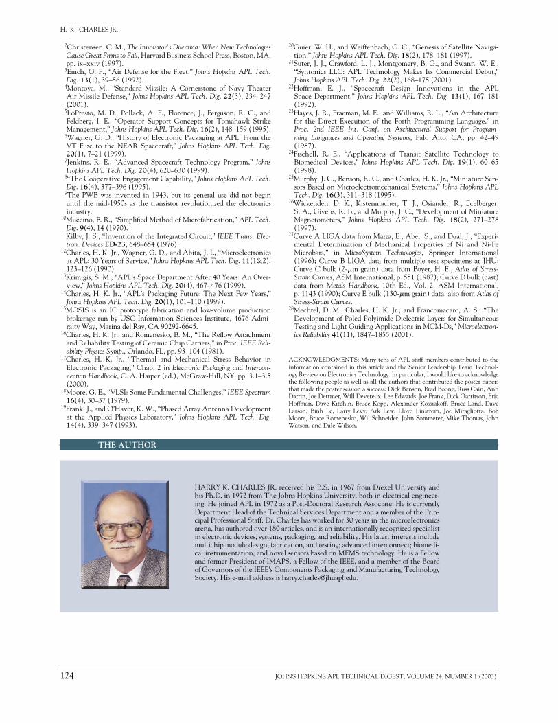
Mechanical properties of representative MEMS materials and layers have been measured for several years under external funding in collaboration with Wil-liam Sharpe of The Johns Hopkins University Mechani-cal Engineering Department. Such collaborations have produced some interesting results, as pesented in Fig. 10.27 The data show that the mechanical properties of thin layers are different from those of their bulk coun-terparts, with the MEMS layers being much stronger. APL MEMS devices have been cycled over 106 times and have demonstrated signifi cant reliability.
In the RF and microwave arenas, our MEMS activities have just begun. These include both a MEMS microwave switch (10 GHz) and a MEMS phase shifter. These units, if successful, could provide a building block for future radar systems. The MEMS switch, shown conceptually in Fig. 11, is a shunt switch design, which promises low insertion loss (0.1 dB) with excellent side-lobe rejection. A microwave phase shifter is currently in the design phase. MEMS fabrication techniques hold great promise for the production of microwave elements (such as switches) at low cost with excellent uniformity and reliability.
APL has successfully transitioned the xylophone magnetometer to a MEMS device (Fig. 12). Its perfor-mance is given in Table 1. The latest measurements and design analyses indicate that MEMS magnetometers can have sensitivities in the 1-nT region. MEMS ther-mal louvers have been developed in collaboration with
Strain (%)
100
200
300
400
500
0
Str
ess
(MP
a)
0 1 2 43 5
A (LIGA)
B (LIGA)
C (bulk)
E (bulk)
D (bulk)
Figure 10. Stress versus strain curves for various nickel test samples.27 The fi gure illustrates that LIGA nickel (A and B) is much stronger than bulk nickel (C, D, and E), with a larger elastic region and Young’s modulus (E = 215 GPa).

JOHNS HOPKINS APL TECHNICAL DIGEST, VOLUME 24, NUMBER 1 (2003) 121
ELECTRONICS TECHNOLOGY AT APL
Ted Swanson at NASA/Goddard Space Flight Center. These louvers consist of movable panels of polysilicon coated with gold metallization. Tilting these panels (Fig. 13) above a horizontal surface changes the emis-sivity (refl ectivity) as a function of angle and thus provides thermal control. The project has progressed to the point where the thermal louvers can be tested in space. A MEMS thermal louvered panel, along with its control circuitry and temperature measurement devices, will ride on the Space Technology 5 (ST-5) mission scheduled for launch in June 2004. Once in space, the louvers’ thermal management capability will be oper-ated as part of a technology demonstration project for NASA’s New Millennium Program.
StrengthsAPL has modest strengths and capabilities in the
MEMS arena. We have facilities for MEMS design, release, and, of course, packaging. Release and pack-aging are key issues for any successful MEMS effort. APL has excellent laboratories and in-place processes
Membrane
Undercut access holes
Lower electrode
Dielectric
Signal path
Top view
Figure 11. Schematic representation of a MEMS microwave switch. An actual switch using this shunt design has been fabri-cated at APL and is undergoing electrical testing.
Figure 12. MEMS implementation of the APL-developed xylo-phone magnetometer. The MEMS version was designed at APL and fabricated using the MUMPS process.
to allow the effective release of MEMS devices on an individual chip or on the entire wafer. Our one-of-a-kind fl exible packaging methods give us real oppor-tunities and advantages. In addition, the Laboratory has recently purchased a deep reactive ion etching system (DRIE). The DRIE will allow three-dimensional etching of features and structures with nearly vertical sidewalls and will give us greater capability to fabricate MEMS on site.
Table 1. Xylophone magnetometer characteristics.
Magnetometer type Values
CuBe xylophone magnetometers (non-MEMS) Length range 2–50 mm Resonance frequency range 1–50 kHz Maximum current 5 A Sensitivity <1 nT Measured mixing frequency range 0–20 GHz
Polysilicon xylophone magnetometers (MEMS) Length range 100–700 �m Resonance frequency range 10–300 kHz Maximum current 0.1 mA Sensitivity <1000 nT
CMOS xylophone magnetometers (MEMS) Length range 100–700 �m Frequency range 10–300 kHz Expected maximum current 100 mA Expected sensitivity <1 nT
Figure 13. MEMS implementation of a thermal louver. This panel uses a proprietary APL hinge design. An array of these panels will be used to change a spacecraft’s surface emissivity during fl ight. A prototype array will fl y in 2004 aboard the ST-5 shuttle mission.

122 JOHNS HOPKINS APL TECHNICAL DIGEST, VOLUME 24, NUMBER 1 (2003)
H. K. CHARLES JR.
We have also taken advantage of the government-sponsored MEMS foundries and have worked out most interface issues during the many tens of foundry runs we have had since the mid-1990s. APL is active in the MEMS community and collaborates with many institutions including NASA/Goddard, NASA/Lang-ley, NASA/Glenn, the Army Research Laboratory, Sandia, and Carnegie Mellon University. These col-laborations as well as participation in the MEMS Alli-ance have allowed APL to develop a reputation as a player in the MEMS community. This connectivity can provide opportunities for APL to grow its MEMS base and activities.
Similarly, our underlying strengths in the design of electronic circuitry, coupled with our knowledge of end-use system applications, afford APL signifi cant potential advantage over several other competitive MEMS activities.
Future Directions and OpportunitiesMEMS work is at a crossroad at APL: Either we
capitalize on our perceived reputation by broaden-ing our MEMS development and applications, or we continue at the current modest pace that is largely dominated by niche applications and the availability of funding, both internal and external. Moving out smartly in the MEMS arena will require some key investments, additional external funding, and the establishment of some longer-term strategic goals. Critical to future success is the ability to select from the myriad MEMS devices and applications the ones that will give APL the competitive advantage in its system development business. Once directions are picked, the necessary equipment, personnel skills, and development processes must be implemented to ensure that we have suffi cient expertise and resource depth to meet the MEMS needs of current and future APL customers.
Particular attention must be paid to developing MEMS design skills and the ability to integrate elec-tronics with the MEMS structures. Efforts have begun in this area via collaborations with G. Fedder at Carn-egie Mellon University on CMOS MEMS devices and with A. Andreou at JHU on silicon-on-sapphire MEMS devices using the Peregrine Foundry. Also, as MEMS activities evolve, greater emphasis needs to be placed on the micro world (i.e., thinking micro for applications and design opportunities) and its associated differences (from the macro world) in materials properties and behavior.
OPTOELECTRONICS/PHOTONICSOptoelectronics or photonics refers to the fi eld that
combines both optics and electronics into a single device, component, or subsystem. Inherent in the words
is the concept that the devices are ultimately integrated to form a complete system function. While full integra-tion is diffi cult, a complex system may contain both dis-crete and integrated components, including fi ber optics, solid-state lasers, and detectors.
APL has approached the optoelectronics/photonics fi eld slowly, building on successes in both the classi-cal optics fi eld and, of course, electronics. Researchers at APL did much early work with lasers ranging from applications in eye health to remote sensing and laser radar. Work on the feasibility of laser weapons and the use of fi ber optics for shipboard communications were all part of our early optical activities. As these macrosystems evolved, people at the Laboratory began to pursue more integrated solutions to optical signal generation, trans-mission, and reception. An independent research and development thrust area on optoelectronics existed for several years in the early 1990s, which set the stage for many of our present activities.
Current CapabilitiesWe have many capabilities that can be applied to
the optoelectronics/photonics arena including our basic long-time skills in optics and our ability to design and fabricate microcircuits and advanced packaging struc-tures. Embryonic work is under way in several areas such as evaluation of state-of-the-art vertical cavity surface emitting lasers for high-speed optical switching applica-tions, new advanced detectors, an all-optical receiver, and integrated lightguides using conventional and doped polymer layers.28 An example of an integrated lightguide created by a doped and electrically aligned polymer structure is shown in Fig. 14. Photonic and optoelectronics capabilities and facilities exist in many departments at APL. While most of these have a more classical optics bent, they have the tools and equipment necessary to develop system applications and evaluate system performance in the fi elds of photonics and elec-tro-optics.
StrengthsAPL has modest strength and capabilities in
optoelectronics and photonics. Our facilities enable system-level development and evaluation activities. In addition, we have a strong base in classical optical system development and the measurement of opti-cal system performance. Although we have limited optoelectronics/photonics design capabilities, the Labo-ratory has both packaging techniques and the ability to fabricate structures containing optically active layers. These one-of-a-kind fl exible packaging and fabrication capabilities have the potential to provide us with real opportunities and advantages in this arena.
Similarly, our underlying strengths in the design and fabrication of electronic circuitry, coupled with our

JOHNS HOPKINS APL TECHNICAL DIGEST, VOLUME 24, NUMBER 1 (2003) 123
ELECTRONICS TECHNOLOGY AT APL
knowledge of end-use applications, afford APL signifi -cant potential advantage as we develop our embryonic optoelectronics/photonics activities.
Future Directions and OpportunitiesOptoelectronics/photonics work at APL is in its
infancy, and we must rapidly move ahead to keep pace with industry. This will require some development in specialized facilities and personnel, along with the set-ting of long-term strategic goals. Critical to future suc-cess will be the ability to selectively focus on optoelec-tronics and photonics technology that will give APL the competitive advantage in our systems development business. Once directions are determined, the necessary equipment, personnel skills, and development processes must be put in place to ensure that optoelectronics and photonics have suffi cient expertise and resource depth to meet the needs of our current and future customers.
SUMMARYFor 60 years, APL has made signifi cant contribu-
tions to programs of national importance ranging from Fleet defense to the exploration of space. Underlying many of these accomplishments, especially those that result in hardware development, is APL’s electronics
Doped
(b)
(a)
Substrate
Doped and poled Doped
Figure 14. Electro-optic lightguide formed using chromophore-doped polyimide. In the poled fi lm, the chromophores have been aligned under a strong electric fi eld. (a) Schematic cross section of a guide. (b) Light containment achieved by an experimental ver-sion of a guide fabricated at APL.
technology. Electronics technology is practiced in at least seven departments at the Laboratory. At the heart of APL’s electronics technology are strong core services involving microelectronics and advanced packaging, RF and microwave circuitry, and embedded computers and programmable devices. Approximately 90% of the annual labor expended in electronics technology (Table 1) is focused in these three areas. The emerging areas of MEMS and optoelectronics/photonics account for only 10% of the effort, but hold signifi cant promise to make key contributions to APL efforts in the future.
Although APL has made important contributions in each of the fi ve areas discussed in this article, opportuni-ties and steps can be taken to enhance the Laboratory’s capabilities in the fi eld. A near-term recommendation is to enhance our capabilities and expertise in our core electronics technologies and foster greater collaboration in these areas across departments and business areas. Flexible processes must be established to support the development needs of the individual business areas while investing in emerging technologies that could have sig-nifi cant future impact. Increased effort must be devoted to effective teaming with partners in government, academia, and industry to leverage technical expertise and resources, especially new or emerging technology resources that could have a signifi cant impact on our future systems business.
In a more fundamental sense, we should continue to seek deep science and engineering expertise in electronics technology and develop strategic think-ing about what electronics capabilities are needed to support emerging business opportunities. For example, optoelectronics/photonics are likely to have a sweeping impact on several of our key business areas during the next few years, and the Laboratory needs to be prepared to take advantage of the new capabilities that these technologies will provide.
Finally, APL should keep its staff current on electron-ics technology, especially the emerging areas of MEMS and optoelectronics/photonics. This knowledge will enable APL to better leverage such expertise to remain competitive and develop new business. As mentioned, one key aspect for obtaining and developing this staff expertise is to encourage our staff to establish collabora-tions and to participate in more professional and govern-ment activities in the electronics technology area. In addition, we must actively engage academia and industry in a deliberate and well-planned manner to ensure that we retain access to the latest developments in electron-ics technology that can readily be applied to the critical challenges facing the Laboratory and the nation.
REFERENCES AND NOTES 1Klingaman, W. K., APL—Fifty Years of Service to the Nation: A History
of The Johns Hopkins University Applied Physics Laboratory, JHU/APL, Laurel, MD, pp. 1–20 (1993).
124 JOHNS HOPKINS APL TECHNICAL DIGEST, VOLUME 24, NUMBER 1 (2003)
H. K. CHARLES JR.
2Christensen, C. M., The Innovator’s Dilemma: When New Technologies Cause Great Firms to Fail, Harvard Business School Press, Boston, MA, pp. ix–xxiv (1997).
3Emch, G. F., “Air Defense for the Fleet,” Johns Hopkins APL Tech. Dig. 13(1), 39–56 (1992).
4Montoya, M., “Standard Missile: A Cornerstone of Navy Theater Air Missile Defense,” Johns Hopkins APL Tech. Dig. 22(3), 234–247 (2001).
5LoPresto, M. D., Pollack, A. F., Florence, J., Ferguson, R. C., and Feldberg, I. E., “Operator Support Concepts for Tomahawk Strike Management,” Johns Hopkins APL Tech. Dig. 16(2), 148–159 (1995).
6Wagner, G. D., “History of Electronic Packaging at APL: From the VT Fuze to the NEAR Spacecraft,” Johns Hopkins APL Tech. Dig. 20(1), 7–21 (1999).
7Jenkins, R. E., “Advanced Spacecraft Technology Program,” Johns Hopkins APL Tech. Dig. 20(4), 620–630 (1999).
8“The Cooperative Engagement Capability,” Johns Hopkins APL Tech. Dig. 16(4), 377–396 (1995).
9The PWB was invented in 1943, but its general use did not begin until the mid-1950s as the transistor revolutionized the electronics industry.
10Muccino, F. R., “Simplifi ed Method of Microfabrication,” APL Tech. Dig. 9(4), 14 (1970).
11Kilby, J. S., “Invention of the Integrated Circuit,” IEEE Trans. Elec-tron. Devices ED-23, 648–654 (1976).
12Charles, H. K. Jr., Wagner, G. D., and Abita, J. L, “Microelectronics at APL: 30 Years of Service,” Johns Hopkins APL Tech. Dig. 11(1&2), 123–126 (1990).
13Krimigis, S. M., “APL’s Space Department After 40 Years: An Over-view,” Johns Hopkins APL Tech. Dig. 20(4), 467–476 (1999).
14Charles, H. K. Jr., “APL’s Packaging Future: The Next Few Years,” Johns Hopkins APL Tech. Dig. 20(1), 101–110 (1999).
15MOSIS is an IC prototype fabrication and low-volume production brokerage run by USC Information Sciences Institute, 4676 Admi-ralty Way, Marina del Ray, CA 90292-6645.
16Charles, H. K. Jr., and Romenesko, B. M., “The Refl ow Attachment and Reliability Testing of Ceramic Chip Carriers,” in Proc. IEEE Reli-ability Physics Symp., Orlando, FL, pp. 93–104 (1981).
17Charles, H. K. Jr., “Thermal and Mechanical Stress Behavior in Electronic Packaging,” Chap. 2 in Electronic Packaging and Intercon-nection Handbook, C. A. Harper (ed.), McGraw-Hill, NY, pp. 3.1–3.5 (2000).
18Moore, G. E., “VLSI: Some Fundamental Challenges,” IEEE Spectrum 16(4), 30–37 (1979).
19Frank, J., and O’Haver, K. W., “Phased Array Antenna Development at the Applied Physics Laboratory,” Johns Hopkins APL Tech. Dig. 14(4), 339–347 (1993).
20Guier, W. H., and Weiffenbach, G. C., “Genesis of Satellite Naviga-tion,” Johns Hopkins APL Tech. Dig. 18(2), 178–181 (1997).
21Suter, J. J., Crawford, L. J., Montgomery, B. G., and Swann, W. E., “Syntonics LLC: APL Technology Makes Its Commercial Debut,” Johns Hopkins APL Tech. Dig. 22(2), 168–175 (2001).
22Hoffman, E. J., “Spacecraft Design Innovations in the APL Space Department,” Johns Hopkins APL Tech. Dig. 13(1), 167–181 (1992).
23Hayes, J. R., Fraeman, M. E., and Williams, R. L., “An Architecture for the Direct Execution of the Forth Programming Language,” in Proc. 2nd IEEE Int. Conf. on Architectural Support for Program-ming Languages and Operating Systems, Palo Alto, CA, pp. 42–49 (1987).
24Fischell, R. E., “Applications of Transit Satellite Technology to Biomedical Devices,” Johns Hopkins APL Tech. Dig. 19(1), 60–65 (1998).
25Murphy, J. C., Benson, R. C., and Charles, H. K. Jr., “Miniature Sen-sors Based on Microelectromechanical Systems,” Johns Hopkins APL Tech. Dig. 16(3), 311–318 (1995).
26Wickenden, D. K., Kistenmacher, T. J., Osiander, R., Ecelberger, S. A., Givens, R. B., and Murphy, J. C., “Development of Miniature Magnetometers,” Johns Hopkins APL Tech. Dig. 18(2), 271–278 (1997).
27Curve A LIGA data from Mazza, E., Abel, S., and Dual, J., “Experi-mental Determination of Mechanical Properties of Ni and Ni-Fe Microbars,” in MicroSystem Technologies, Springer International (1996); Curve B LIGA data from multiple test specimens at JHU; Curve C bulk (2-�m grain) data from Boyer, H. E., Atlas of Stress-Strain Curves, ASM International, p. 551 (1987); Curve D bulk (cast) data from Metals Handbook, 10th Ed., Vol. 2, ASM International, p. 1143 (1990); Curve E bulk (130-�m grain) data, also from Atlas of Stress-Strain Curves.
28Mechtel, D. M., Charles, H. K. Jr., and Francomacaro, A. S., “The Development of Poled Polyimide Dielectric Layers for Simultaneous Testing and Light Guiding Applications in MCM-Ds,” Microelectron-ics Reliability 41(11), 1847–1855 (2001).
ACKNOWLEDGMENTS: Many tens of APL staff members contributed to the information contained in this article and the Senior Leadership Team Technol-ogy Review on Electronics Technology. In particular, I would like to acknowledge the following people as well as all the authors that contributed the poster papers that made the poster session a success: Dick Benson, Brad Boone, Russ Cain, Ann Darrin, Joe Dettmer, Will Devereux, Lee Edwards, Joe Frank, Dick Garritson, Eric Hoffman, Dave Kitchin, Bruce Kopp, Alexander Kossiakoff, Bruce Land, Dave Larson, Binh Le, Larry Levy, Ark Lew, Lloyd Linstrom, Joe Miragliotta, Bob Moore, Bruce Romenesko, Wil Schneider, John Sommerer, Mike Thomas, John Watson, and Dale Wilson.
THE AUTHOR
HARRY K. CHARLES JR. received his B.S. in 1967 from Drexel University and his Ph.D. in 1972 from The Johns Hopkins University, both in electrical engineer-ing. He joined APL in 1972 as a Post-Doctoral Research Associate. He is currently Department Head of the Technical Services Department and a member of the Prin-cipal Professional Staff. Dr. Charles has worked for 30 years in the microelectronics arena, has authored over 180 articles, and is an internationally recognized specialist in electronic devices, systems, packaging, and reliability. His latest interests include multichip module design, fabrication, and testing; advanced interconnect; biomedi-cal instrumentation; and novel sensors based on MEMS technology. He is a Fellow and former President of IMAPS, a Fellow of the IEEE, and a member of the Board of Governors of the IEEE’s Components Packaging and Manufacturing Technology Society. His e-mail address is [email protected].