electronics - especmonitor.espec.ws/files/samsung_vp-d451__d453__d454__d455__d662… · samsung...
TRANSCRIPT

DIGITAL VIDEO CAMCORDERChassis : Tiger BASIC : VP-D455Application Models : VP-D451(I)/VP-D453(I)/
VP-D454(I)/VP-D455(I)/VP-D6620I/VP-D6650I
Application Area: XEF, XEU, XEG, XET, XEV, XEC, XSA, CDM,
XST, XEO, XEH, XEP, XEE, EAP, EUR, XEN, HACO, TAW, TIT, COL, SEO, XSS, SED, XSH,XSG, FES, XTL, CHN, ZAM, STS, SMR, XFA, ITN, KNT, XSE, FPT, RAD
SERVICE Ultra Compact Design DVC
Use Built-in Flash Memory (VP-D454(i)/D455(i)/D6650I Only)
Multi Memory Card Slot(VP-D454(i)/D455(i)/D6650I Only)
Direct Print System : PictBridge ™
USB 2.0
High quality MPEG4
Digital Image Stabilizer
Real Wide mode (16:9)
Manual
DIGITAL VIDEO CAMCORDER Merit & Character regarding Product
SERVICE MA
NU
AL
VP-D451(I)/D
453(I)/D454(I)/D
455(I)/D6620I/D
6650I
ELECTRONICS
© Samsung Electronics Co., Ltd. FEB. 2005Printed in KoreaAD82-00104A
This Service Manual is a property of Samsung Electronics Co .,Ltd.Any unauthorized use of Manual can be punished under applicable
International and/or domestic law.

This Document can not be used without Samsung’s authorizationSamsung Electronics 7-1
7. Block Diagrams
� �
� �
KS7221D
LA70056TB
LB11993W
LC74132W
K4S283233F
K8D16UBA
CXM3009TQ
BU7806
NJM2567
TLV990B
UPD168103
V.DRIVE
CDS/AGC/ADC
ZOOM/FOCUSM.DRIVE
CAMERAPROCESS
ZOOM/TG/DIS
128M DRAM
16M NOR
Built-inMEMORY
MOTORDRIVE
PREAMP IC
PRML IC
AUDIO I/O I/F
VIDDEO OUT
LCD/CVF DRIVE
x10 DVC Lens
DSP6S5C7376X
MULTI Memory Slot
MULTI Stick Slot
TMP1962
24C045STPXC61FC2512
RS5C372A
MAIN MICOM
E2PROM RESET
TIMER
SONY LCO2.5" 123K
SONY CVF0.24"77K
Link/PhyLayer ECC
MODDEMODDCT/IDCT
COMPDECOMP
AUDIO
DecimationADC/DAC
ShuffleVideo ENC
VideoDecorder
4M DRAM
10.5M DRAM
D
E
C
K
FUNCION
POWER
3.0V�1.8V�2.5V�5.0V�15V�12V�
-7.5V�-15V
ITU6�5�6��
C�A�M
USB
MIC
AUDDIO IN/OUT
VIDDEO IN/OUT
DV IN/OUT
S-Y IN
S-C IN
CCDLens
OLPF
ITU656
VCR
GDCLCD
GDCMON
CLK
(VP-D454(I)/D455(I)/D6550I)
(VP-D454(I)/D455(I)/D6550I)
(VP-D453(I)/D6620I)
7-1 All Block Diagram
Block Diagrams
7-2 Samsung ElectronicsThis Document can not be used without Samsung’s authorization
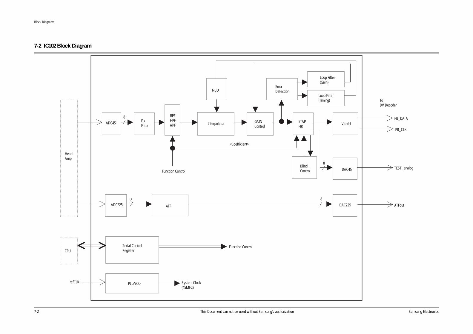
HeadAmp
CPU
ADC45
ADC225 ATF
GAINControl
Loop Filter(Gain)
Loop Filter(Timing)
Viterbi
DAC225
DAC45
ATFout
TEST_analog
PB_CLK
PB_DATA
NCO
PLL/VCO System Clock(45MHz)
Function Control
Function Control
FixFilter Interpolator
BPFHPFAPF
Serial ControlRegister
ErrorDetection
5TAPFIR
BlindControl
refCLK
ToDV Decoder
<Coefficient>
8
8
8
8
7-2 IC102 Block Diagram

Block Diagrams
Samsung Electronics 7-3This Document can not be used without Samsung’s authorization
CAMERAPROCESSOR
MPEG4CODEC
(30FPS@VGA)
JPEGCODEC
VIDEO BUS
AHB BUS
ARM920T
AHB2VIDEOBRIDGE
AP
B B
US
AHB2APBBRIDGE
USB 2.0 DEV.
UART * 2
AUDIOCODEC(G.726)
MS ProSD/MMC
Timer * 4
GPIO(32bit)
DNIe
DMA * 4
DVCDSP
I2C*2Motor
ControlPWM2ch
I2S
SPI * 2OSD
AD 4ch(200KHz/
10bit)
DRAMController(for F/W)
NANDFLASH
CONTROLLER
7-3 IC201 Block Diagram

Block Diagrams
7-4 Samsung ElectronicsThis Document can not be used without Samsung’s authorization
CAMERAPROCESSOR
MPEG4CODEC
(30FPS@VGA)
JPEGCODEC
VIDEO BUS
AHB BUS
ARM920T
AHB2VIDEOBRIDGE
AP
B B
US
AHB2APBBRIDGE
USB 2.0 DEV.
UART * 2
AUDIOCODEC(G.726)
MS ProSD/MMC
Timer * 4
GPIO(32bit)
DNIe
DMA * 4
DVCDSP
I2C*2Motor
ControlPWM2ch
I2S
SPI * 2OSD
AD 4ch(200KHz/
10bit)
DRAMController(for F/W)
NANDFLASH
CONTROLLER
7-4 ICM01 Block Diagram

Samsung Electronics 8-1
8. Wiring Diagram
MEMORY STICK (VP-D453(I)/D6620I)(VP-D454(I)/D455(I)/D6650I)

Wiring Diagram
8-2 Samsung Electronics
MEMO
This Document can not be used without Samsung’s authorizationSamsung Electronics 10-1
10. Schematic Diagrams
10-1 DC/DC Converter (Main PCB) - - - - - - - - - - - - - - - - - - - - - - - - - - - - - - - - 10-2
10-2 Servo (Main PCB) - - - - - - - - - - - - - - - - - - - - - - - - - - - - - - - - - - - - - - - - 10-3
10-3 System Control (Main PCB) - - - - - - - - - - - - - - - - - - - - - - - - - - - - - - - - - 10-4
10-4 Pre Amp/PRML (Main PCB) - - - - - - - - - - - - - - - - - - - - - - - - - - - - - - - - - 10-5
10-5 DV-1Chip (Main PCB) - - - - - - - - - - - - - - - - - - - - - - - - - - - - - - - - - - - - - 10-6
10-6 Video-Interface (Main PCB) - - - - - - - - - - - - - - - - - - - - - - - - - - - - - - - - - 10-7
10-7 Audio (Main PCB)- - - - - - - - - - - - - - - - - - - - - - - - - - - - - - - - - - - - - - - - 10-8
10-8 Camera Process (Main PCB) - - - - - - - - - - - - - - - - - - - - - - - - - - - - - - - - 10-9
10-9 DSP (Main PCB) - - - - - - - - - - - - - - - - - - - - - - - - - - - - - - - - - - - - - - - - - 10-10
10-10 Camera Memory 1 (Main PCB) - - - - - - - - - - - - - - - - - - - - - - - - - - - - - - 10-11
10-11 Camera Memory 2 (Main PCB) - - - - - - - - - - - - - - - - - - - - - - - - - - - - - - 10-12
10-12 CCD (CCD PCB) - - - - - - - - - - - - - - - - - - - - - - - - - - - - - - - - - - - - - - - - - 10-13
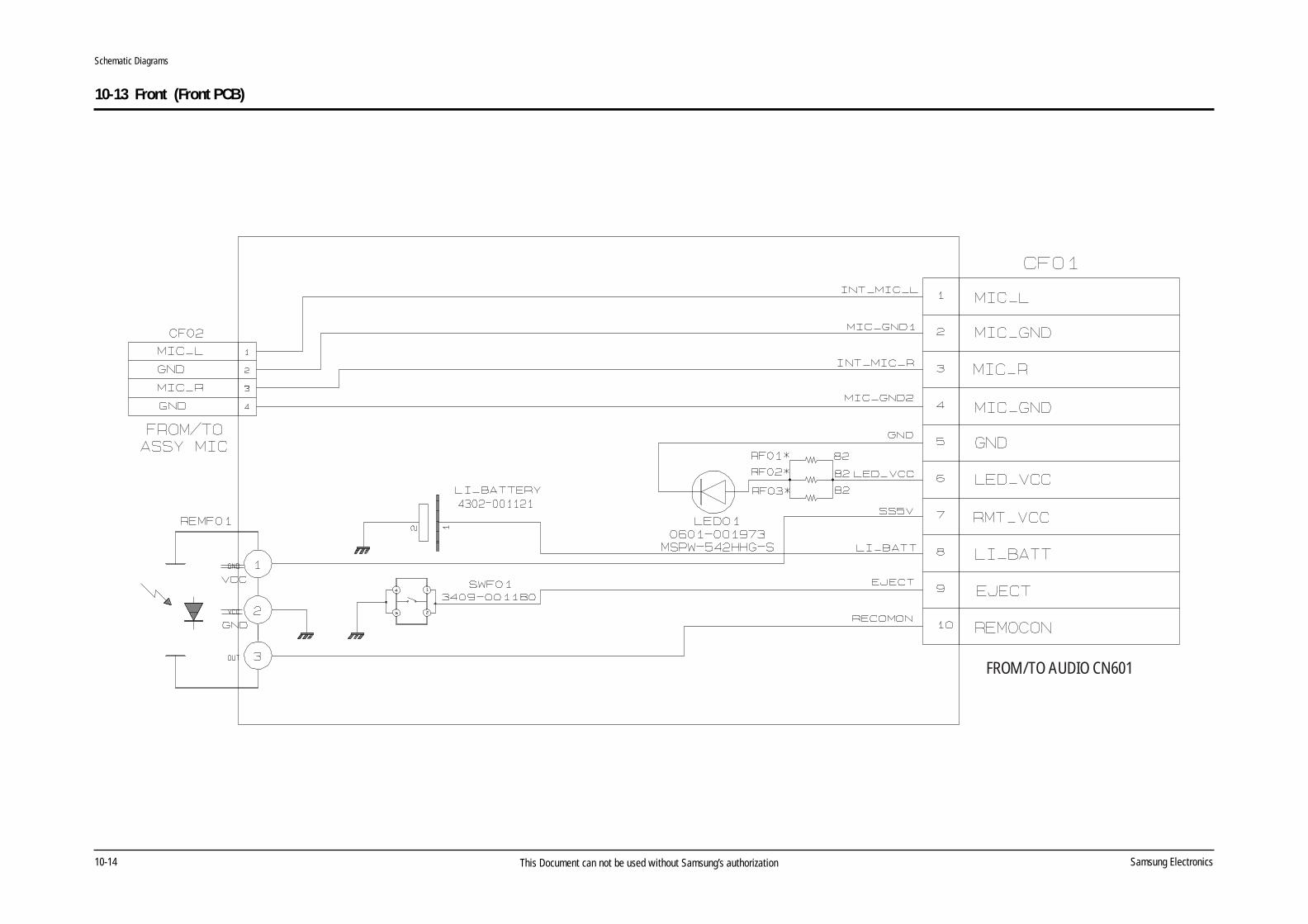
10-13 Front (Front PCB)- - - - - - - - - - - - - - - - - - - - - - - - - - - - - - - - - - - - - - - - 10-14
10-14 Jack (Jack PCB) - - - - - - - - - - - - - - - - - - - - - - - - - - - - - - - - - - - - - - - - 10-15
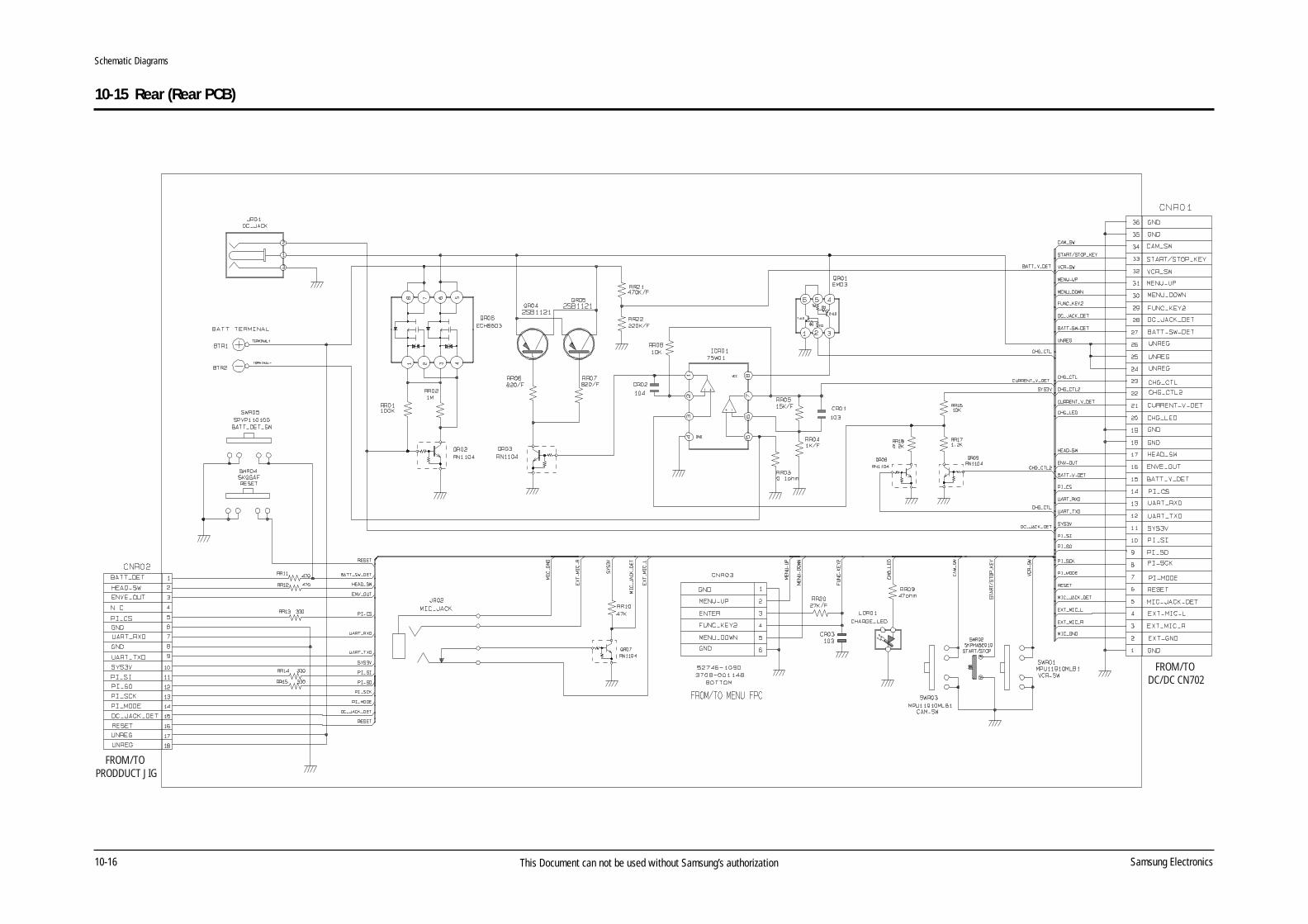
10-15 Rear (Rear PCB) - - - - - - - - - - - - - - - - - - - - - - - - - - - - - - - - - - - - - - - - 10-16
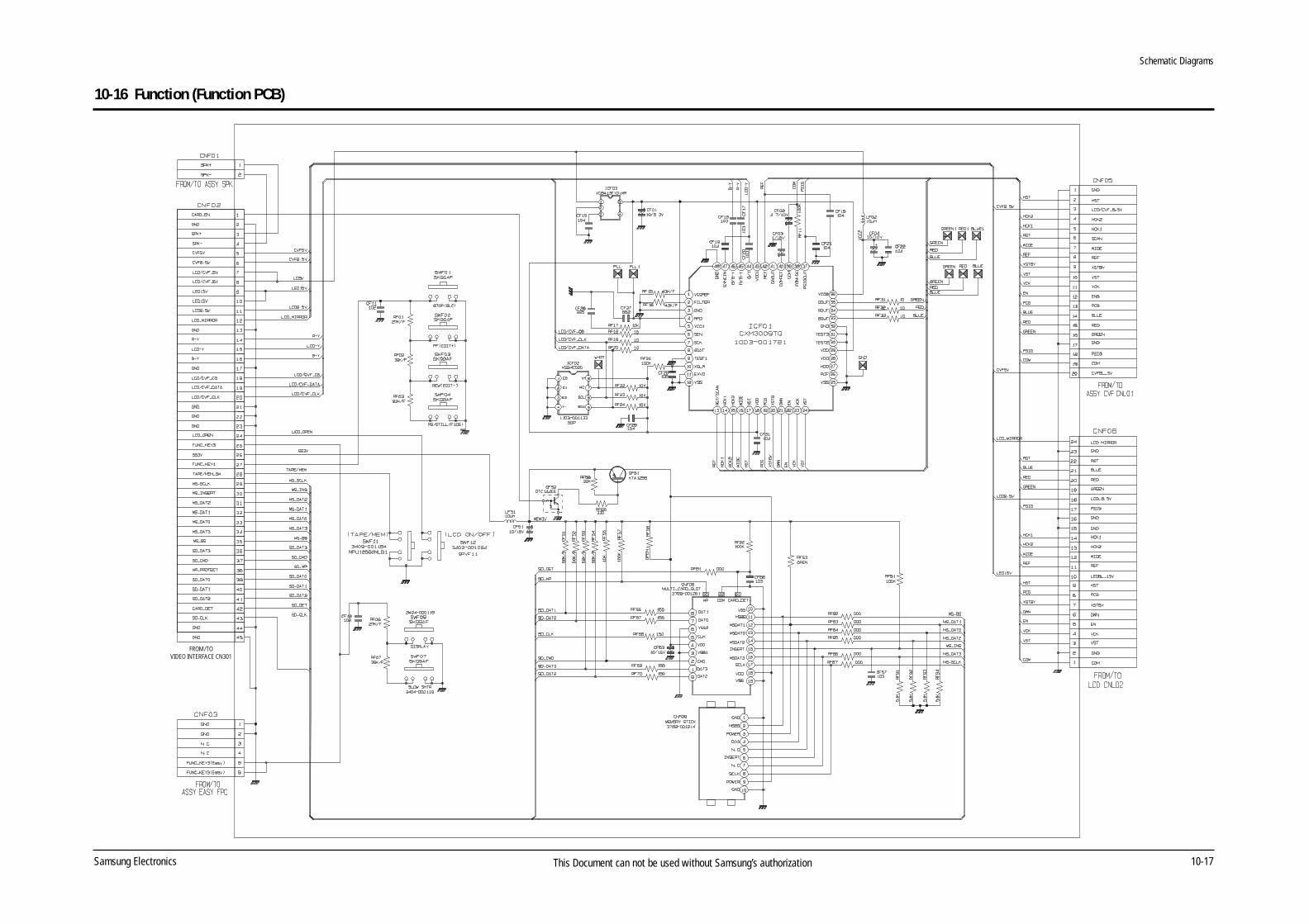
10-16 Function (Function PCB)- - - - - - - - - - - - - - - - - - - - - - - - - - - - - - - - - - - 10-17
10-17 CVF (CVF PCB) - - - - - - - - - - - - - - - - - - - - - - - - - - - - - - - - - - - - - - - - - 10-18
10-18 LCD (LCD PCB) - - - - - - - - - - - - - - - - - - - - - - - - - - - - - - - - - - - - - - - - - 10-19
For schematic Diagram- Resistors are in ohms, 1/8W unless otherwise noted.
Note
Special note : Most semiconductor devices are electrostatically sensitive and therefore require the special handling techniques described under the “electrostatically sensitive (ES) devices” section of this service manual.
Note : Do not use the part number shown on this drawing for ordering. The correct part number is shown in the parts list (may be slightly
different or amended since this drawing was prepared).
Important safety notices : Components identified with the mark have the special characteristics for safety. When replacing any of these components. Use only the same type.
Page

Schematic Diagrams
10-2 Samsung ElectronicsThis Document can not be used without Samsung’s authorization
10-1 DC/DC Converter (Main PCB)

Schematic Diagrams
Samsung Electronics 10-3This Document can not be used without Samsung’s authorization
10-2 Servo (Main PCB)

Schematic Diagrams
10-4 Samsung ElectronicsThis Document can not be used without Samsung’s authorization
FROM/TOTEST JIG
10-3 System Control (Main PCB)

Schematic Diagrams
Samsung Electronics 10-5This Document can not be used without Samsung’s authorization
10-4 Pre Amp/PRML (Main PCB)

Schematic Diagrams
10-6 Samsung ElectronicsThis Document can not be used without Samsung’s authorization
10-5 DV-1Chip (Main PCB)

Schematic Diagrams
Samsung Electronics 10-7This Document can not be used without Samsung’s authorization
10-6 Video-Interface (Main PCB)

Schematic Diagrams
10-8 Samsung ElectronicsThis Document can not be used without Samsung’s authorization
10-7 Audio (Main PCB)
Schematic Diagrams
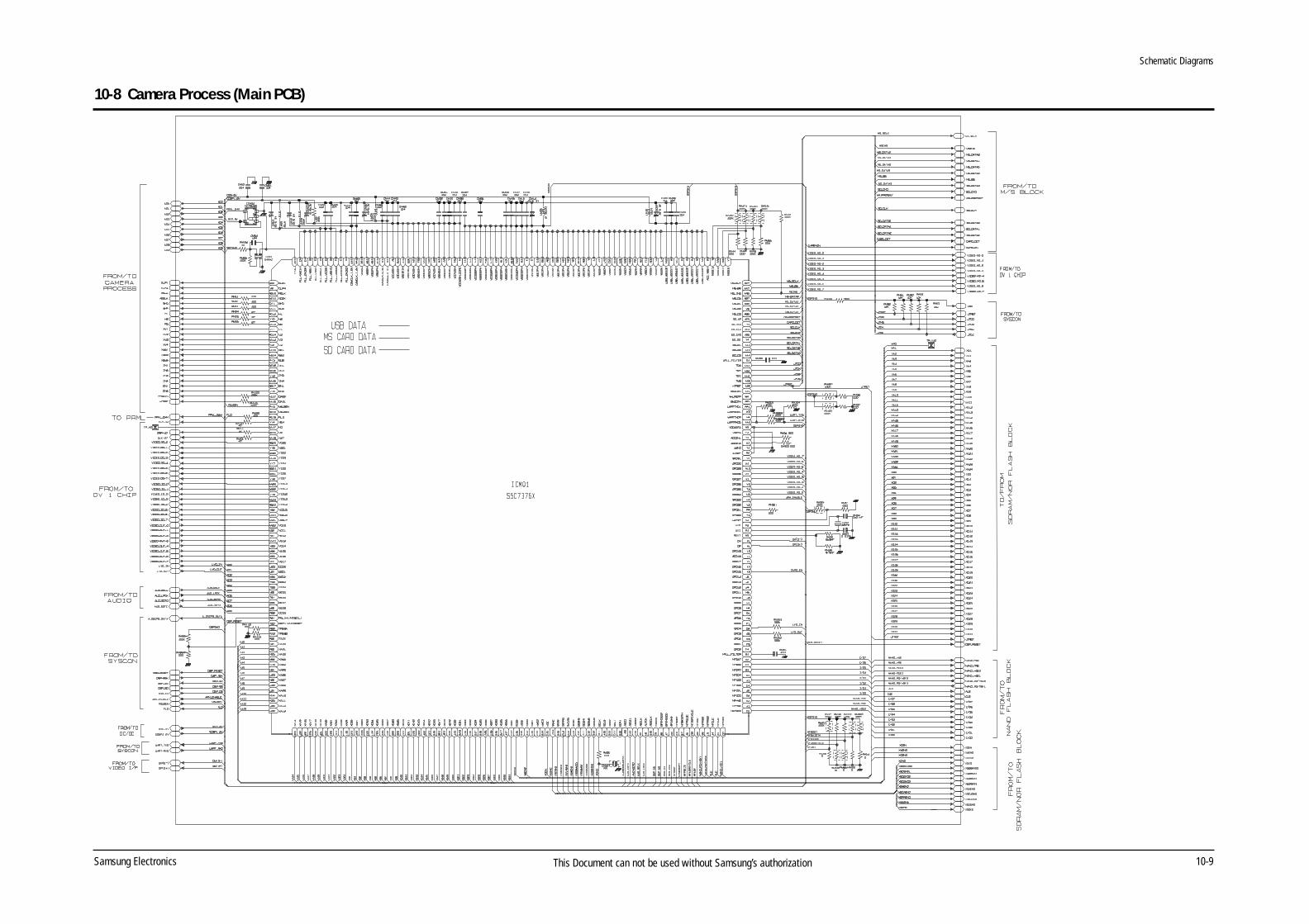
Samsung Electronics 10-9This Document can not be used without Samsung’s authorization
10-8 Camera Process (Main PCB)

Schematic Diagrams
10-10 Samsung ElectronicsThis Document can not be used without Samsung’s authorization
10-9 DSP (Main PCB)

Schematic Diagrams
Samsung Electronics 10-11This Document can not be used without Samsung’s authorization
10-10 Camera Memory 1 (Main PCB)

Schematic Diagrams
10-12 Samsung ElectronicsThis Document can not be used without Samsung’s authorization
10-11 Camera Memory 2 (Main PCB)
Schematic Diagrams
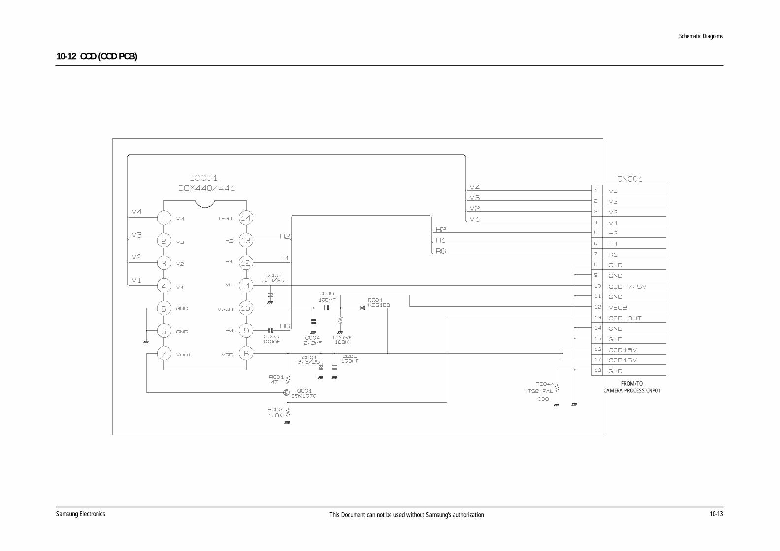
Samsung Electronics 10-13This Document can not be used without Samsung’s authorization
FROM/TOCAMERA PROCESS CNP01
10-12 CCD (CCD PCB)
Schematic Diagrams
10-14 Samsung ElectronicsThis Document can not be used without Samsung’s authorization
FROM/TO AUDIO CN601
10-13 Front (Front PCB)

Schematic Diagrams
Samsung Electronics 10-15This Document can not be used without Samsung’s authorization
FROM/TO VIDEO INTERFACE CN302
10-14 Jack (Jack PCB)
Schematic Diagrams
10-16 Samsung ElectronicsThis Document can not be used without Samsung’s authorization
FROM/TO PRODDUCT JIG
FROM/TO DC/DC CN702
10-15 Rear (Rear PCB)
Schematic Diagrams
Samsung Electronics 10-17This Document can not be used without Samsung’s authorization
FROM/TOVIDEO INTERFACE CN301
10-16 Function (Function PCB)

Schematic Diagrams
10-18 Samsung ElectronicsThis Document can not be used without Samsung’s authorization
FROM/TO FUNCTION CNF05
FROM/TO CVF PANEL
10-17 CVF (CVF PCB)

Schematic Diagrams
Samsung Electronics 10-19This Document can not be used without Samsung’s authorization
10-18 LCD (LCD PCB)

Schematic Diagrams
10-20 Samsung ElectronicsThis Document can not be used without Samsung’s authorization
MEMO