electronics laboratory and students’ kits for self-study ...fahed.com/files/eleclab.pdf ·...
TRANSCRIPT

Electronics Laboratory
And Students’ kits
For Self-Study
And Distant Learning
By: Charbel T. Fahed

Table of Contents
I. DC and AC fundamentals
1) Color Code 2) Ohm’s Law 3) Series Circuits 4) Parallel Circuits 5) Series-Parallel Circuits 6) Voltmeter Loading 7) Superposition Theorem 8) Thevenin’s Theorem 9) Wheatstone Bridge 10) RC Wave Shapes
II. Logic Circuits and Systems
1) The breadboard and logic designer 2) Logic Gates 3) Gates Equivalents 4) Combinational Logic Networks 5) Digital Multiplexers/Data Selectors 6) Latches 7) Flip-Flops 8) Four-Bit Ripple Counter 9) 555 Timer
III. AC Circuits
1) Oscilloscope Operation 2) Reactance of Capacitors 3) Series LR Circuits 4) Frequency Response Of RC Circuits 5) Impedance of LRC Circuits 6) Impedance of Parallel RC, RL, and RLC Circuits 7) Characteristics of Series Resonant Circuits 8) Tank Circuit Filter 9) Iron Core Transformer
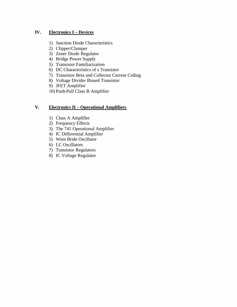
IV. Electronics I – Devices
1) Junction Diode Characteristics 2) Clipper/Clamper 3) Zener Diode Regulator 4) Bridge Power Supply 5) Transistor Familiarization 6) DC Characteristics of s Transistor 7) Transistor Beta and Collector Current Ceiling 8) Voltage Divider Biased Transistor 9) JFET Amplifier 10) Push-Pull Class B Amplifier
V. Electronics II – Operational Amplifiers
1) Class A Amplifier 2) Frequency Effects 3) The 741 Operational Amplifier 4) IC Differential Amplifier 5) Wien Bride Oscillator 6) LC Oscillators 7) Transistor Regulators 8) IC Voltage Regulator

LAB REPORT OUTLINE FOR ELECTRONIC EXPERIMENTS 1. Explain objective of experiment. 2. What are you going to measure? 3. What do you expect the results to be? 4. Divide experiment into parts.
a) Show measurements and results for each part. b) Make sure that each step clearly shows what circuit was used plus the corresponding
waveforms, amplitude, frequency, etc... 5. Conclusions
a) Did the experiment verify what you expected?
b) Were there any unexpected or surprising results? Grading Will Be Based On:
1. Neatness 2. Organization of Material 3. Explanation 4. Correctness 5. Grammar and Spelling 6. Style
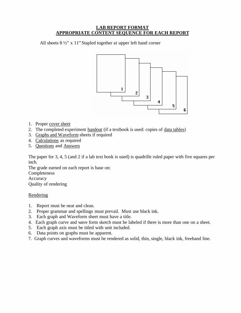
LAB REPORT FORMAT APPROPRIATE CONTENT SEQUENCE FOR EACH REPORT
All sheets 8 ½” x 11” Stapled together at upper left hand corner
1. Proper cover sheet
2. The completed experiment handout (if a textbook is used: copies of data tables) 3. Graphs and Waveform sheets if required 4. Calculations as required 5. Questions and Answers
The paper for 3, 4, 5 (and 2 if a lab text book is used) is quadrille ruled paper with five squares per inch. The grade earned on each report is base on: Completeness Accuracy Quality of rendering Rendering
1. Report must be neat and clean. 2. Proper grammar and spellings must prevail. Must use black ink. 3. Each graph and Waveform sheet must have a title. 4. Each graph curve and wave form sketch must be labeled if there is more than one on a sheet. 5. Each graph axis must be titled with unit included. 6. Data points on graphs must be apparent. 7. Graph curves and waveforms must be rendered as solid, thin, single, black ink, freehand line.
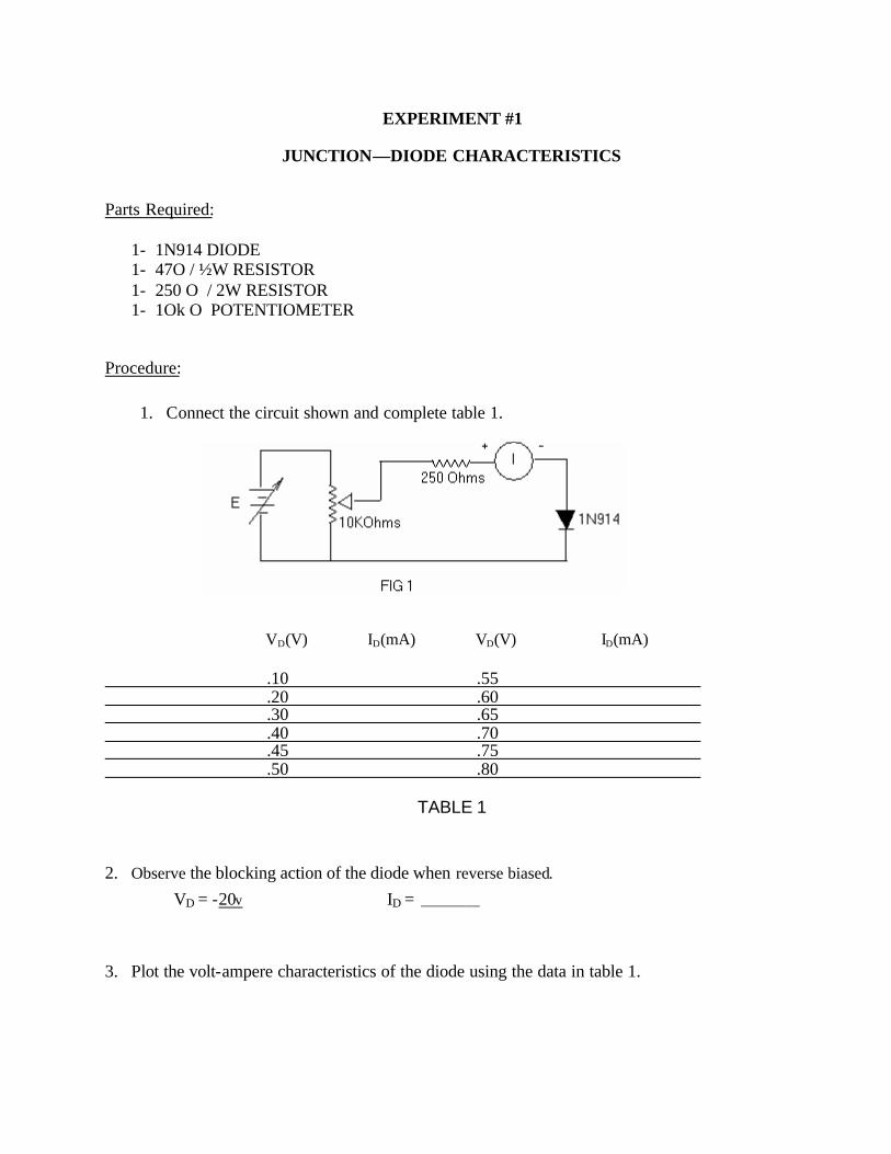
EXPERIMENT #1
JUNCTION—DIODE CHARACTERISTICS
Parts Required: 1- 1N914 DIODE 1- 47O / ½W RESISTOR 1- 250 O / 2W RESISTOR 1- 1Ok O POTENTIOMETER
Procedure:
1. Connect the circuit shown and complete table 1.
VD(V) ID(mA) VD(V) ID(mA) .10 .55 .20 .60 .30 .65 .40 .70 .45 .75 .50 .80
TABLE 1
2. Observe the blocking action of the diode when reverse biased.
VD = -20v ID = ________
3. Plot the volt-ampere characteristics of the diode using the data in table 1.
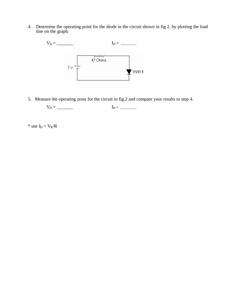
4. Determine the operating point for the diode in the circuit shown in fig 2. by plotting the load line on the graph. VD = _______ ID = ________
5. Measure the operating point for the circuit in fig.2 and compare your results to step 4.
VD = _______ ID = ________
* use ID = VR/R
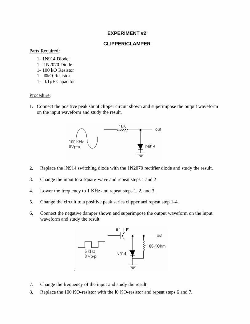
EXPERIMENT #2
CLIPPER/CLAMPER Parts Required:
1- 1N914 Diode; 1- 1N2070 Diode 1- 100 kO Resistor 1- l0kO Resistor 1- 0.1µF Capacitor
Procedure: 1. Connect the positive peak shunt clipper circuit shown and superimpose the output waveform on the input waveform and study the result.
2. Replace the lN914 switching diode with the 1N2070 rectifier diode and study the result. 3. Change the input to a square-wave and repeat steps 1 and 2 4. Lower the frequency to 1 KHz and repeat steps 1, 2, and 3. 5. Change the circuit to a positive peak series clipper and repeat step 1-4. 6. Connect the negative damper shown and superimpose the output waveform on the input waveform and study the result
.
7. Change the frequency of the input and study the result.
8. Replace the 100 KO-resistor with the l0 KO-resistor and repeat steps 6 and 7.

Questions:
1. What conclusions can be drawn from your observations in step 1- 4?
2. As in question #1 but for step 5?
3. As in question #1 but for step 6-8?
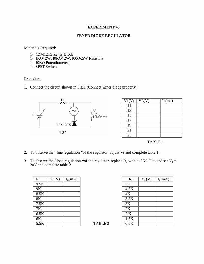
EXPERIMENT #3
ZENER DIODE REGULATOR
Materials Required:
1- 1ZM12T5 Zener Diode 1- lKO/ 2W; l0KO/ 2W; l00O/.5W Resistors 1- l0KO Potentiometer; 1- SPST Switch
Procedure: 1. Connect the circuit shown in Fig.1 (Connect Zener diode properly)
V1(V) VL(V) Iz(ma)
11 13 15 17 19 21 23
TABLE 1
2. To observe the “line regulation “of the regulator, adjust V1 and complete table 1. 3. To observe the “load regulation “of the regulator, replace RL with a l0KO Pot, and set V1 =
20V and complete table 2.
RL VL(V) Iz(mA) RL VL(V) Iz(mA) 9.5K 5K 9K 4.5K 8.5K 4K 8K 3.5K 7.5K 3K 7K 2K 6.5K 2.K 6K 1.5K 5.5K TABLE 2 0.5K
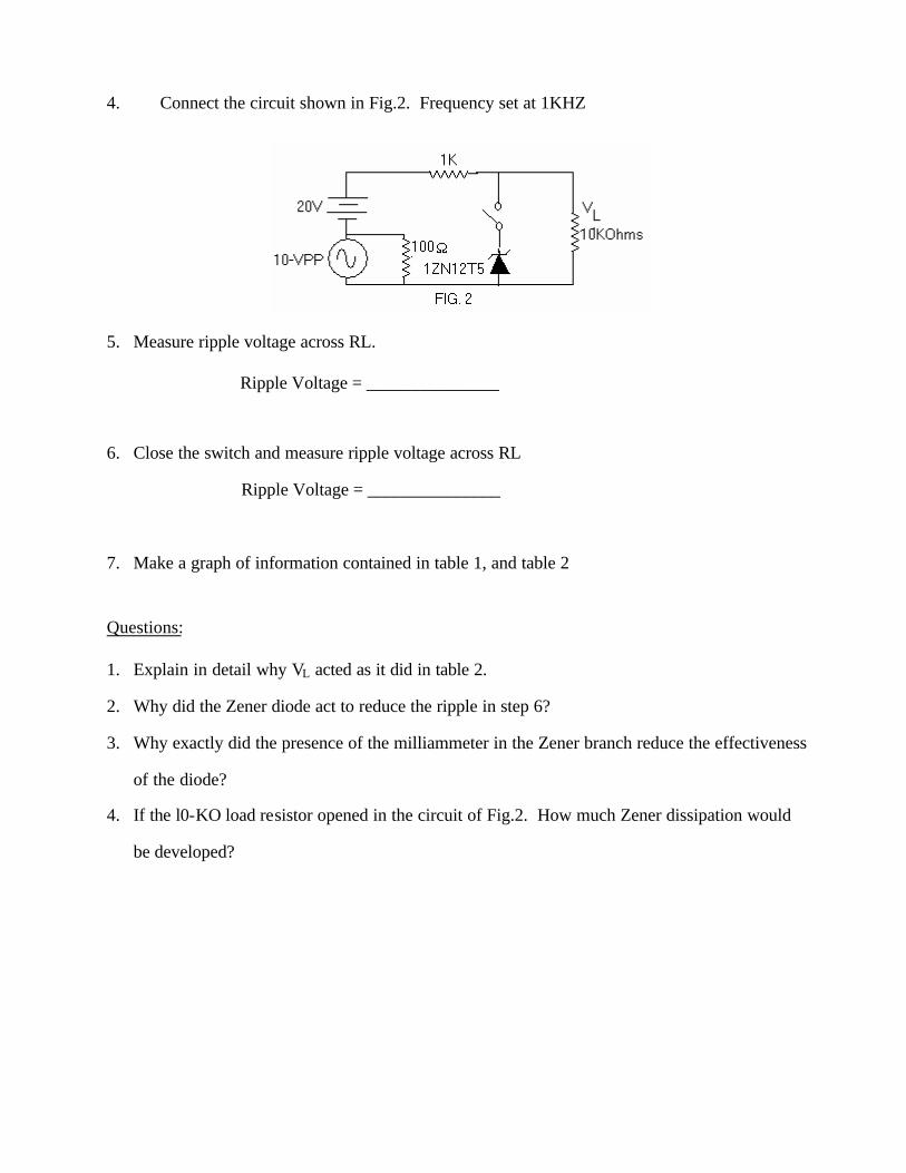
4. Connect the circuit shown in Fig.2. Frequency set at 1KHZ
5. Measure ripple voltage across RL. Ripple Voltage = _______________
6. Close the switch and measure ripple voltage across RL
Ripple Voltage = _______________
7. Make a graph of information contained in table 1, and table 2 Questions:
1. Explain in detail why VL acted as it did in table 2.
2. Why did the Zener diode act to reduce the ripple in step 6?
3. Why exactly did the presence of the milliammeter in the Zener branch reduce the effectiveness
of the diode?
4. If the l0-KO load resistor opened in the circuit of Fig.2. How much Zener dissipation would
be developed?
EXPERIMENT #4
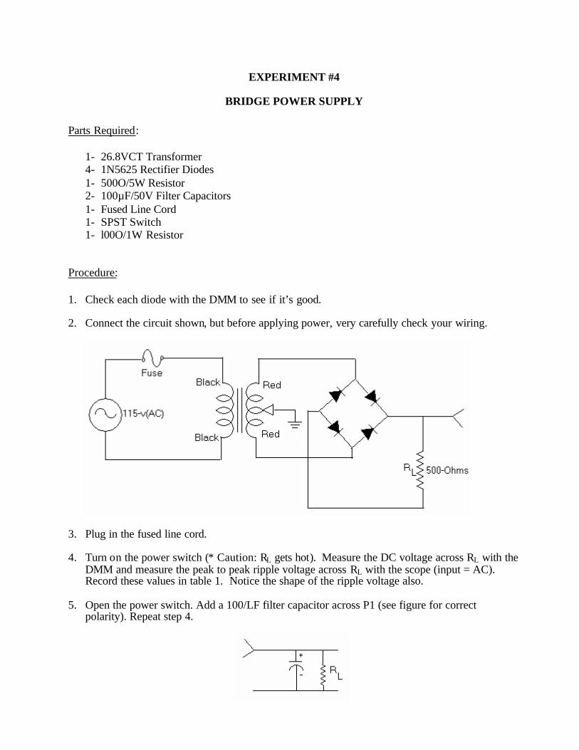
BRIDGE POWER SUPPLY Parts Required:
1- 26.8VCT Transformer 4- 1N5625 Rectifier Diodes 1- 500O/5W Resistor 2- 100µF/50V Filter Capacitors 1- Fused Line Cord 1- SPST Switch 1- l00O/1W Resistor
Procedure: 1. Check each diode with the DMM to see if it’s good. 2. Connect the circuit shown, but before applying power, very carefully check your wiring.
3. Plug in the fused line cord. 4. Turn on the power switch (* Caution: RL gets hot). Measure the DC voltage across RL with the
DMM and measure the peak to peak ripple voltage across RL with the scope (input = AC). Record these values in table 1. Notice the shape of the ripple voltage also.
5. Open the power switch. Add a 100/LF filter capacitor across P1 (see figure for correct polarity). Repeat step 4.
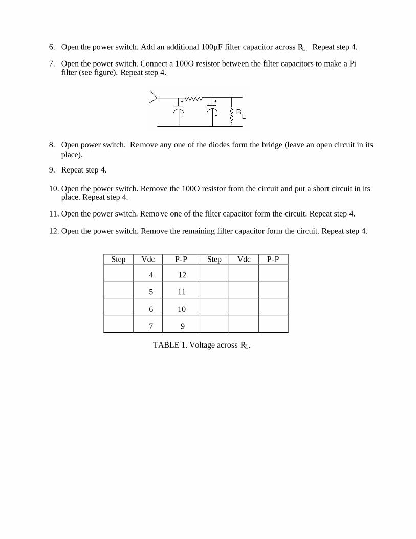
6. Open the power switch. Add an additional 100µF filter capacitor across RL. Repeat step 4. 7. Open the power switch. Connect a 100O resistor between the filter capacitors to make a Pi filter (see figure). Repeat step 4.
8. Open power switch. Remove any one of the diodes form the bridge (leave an open circuit in its place).
9. Repeat step 4. 10. Open the power switch. Remove the 100O resistor from the circuit and put a short circuit in its place. Repeat step 4. 11. Open the power switch. Remove one of the filter capacitor form the circuit. Repeat step 4. 12. Open the power switch. Remove the remaining filter capacitor form the circuit. Repeat step 4.
Step Vdc P-P Step Vdc P-P
4 12
5 11
6 10
7 9
TABLE 1. Voltage across RL.
EXPERIMENT #5
TRANSISTOR FAMILIARIZATION While working in electronics you’ll encounter many transistors. Transistors are composed primarily of either silicon (Si) or germanium (Ge).
As is the case with solid, state diodes, the transistors that are germanium will indicate lower measured resistance values than those that are silicon.
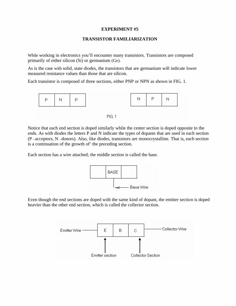
Each transistor is composed of three sections, either PNP or NPN as shown in FIG. 1.
Notice that each end section is doped similarly while the center section is doped opposite to the ends. As with diodes the letters P and N indicate the types of dopants that are used in each section (P = acceptors, N = donors). Also, like diodes, transistors are monocrystalline. That is, each section is a continuation of the growth of’ the preceding section. Each section has a wire attached; the middle section is called the base.
Even though the end sections are doped with the same kind of dopant, the emitter section is doped heavier than the other end section, which is called the collector section.
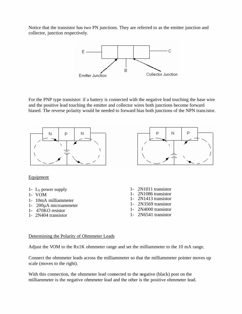
Notice that the transistor has two PN junctions. They are referred to as the emitter junction and collector, junction respectively.
For the PNP type transistor: if a battery is connected with the negative lead touching the base wire and the positive lead touching the emitter and collector wires both junctions become forward biased. The reverse polarity would be needed to forward bias both junctions of the NPN trans istor.
Equipment 1- LV power supply 1- VOM 1- 10mA milliammeter 1- 200µA microammeter 1- 470KO resistor 1- 2N404 transistor
1- 2N1011 transistor 1- 2N1086 transistor 1- 2N1413 transistor 1- 2N3569 transistor 1- 2N4000 transistor 1- 2N6541 transistor
Determining the Polarity of Ohmmeter Leads Adjust the VOM to the Rx1K ohmmeter range and set the milliammeter to the 10 mA range. Connect the ohmmeter leads across the milliammeter so that the milliammeter pointer moves up scale (moves to the right). With this connection, the ohmmeter lead connected to the negative (black) post on the milliammeter is the negative ohmmeter lead and the other is the positive ohmmeter lead.
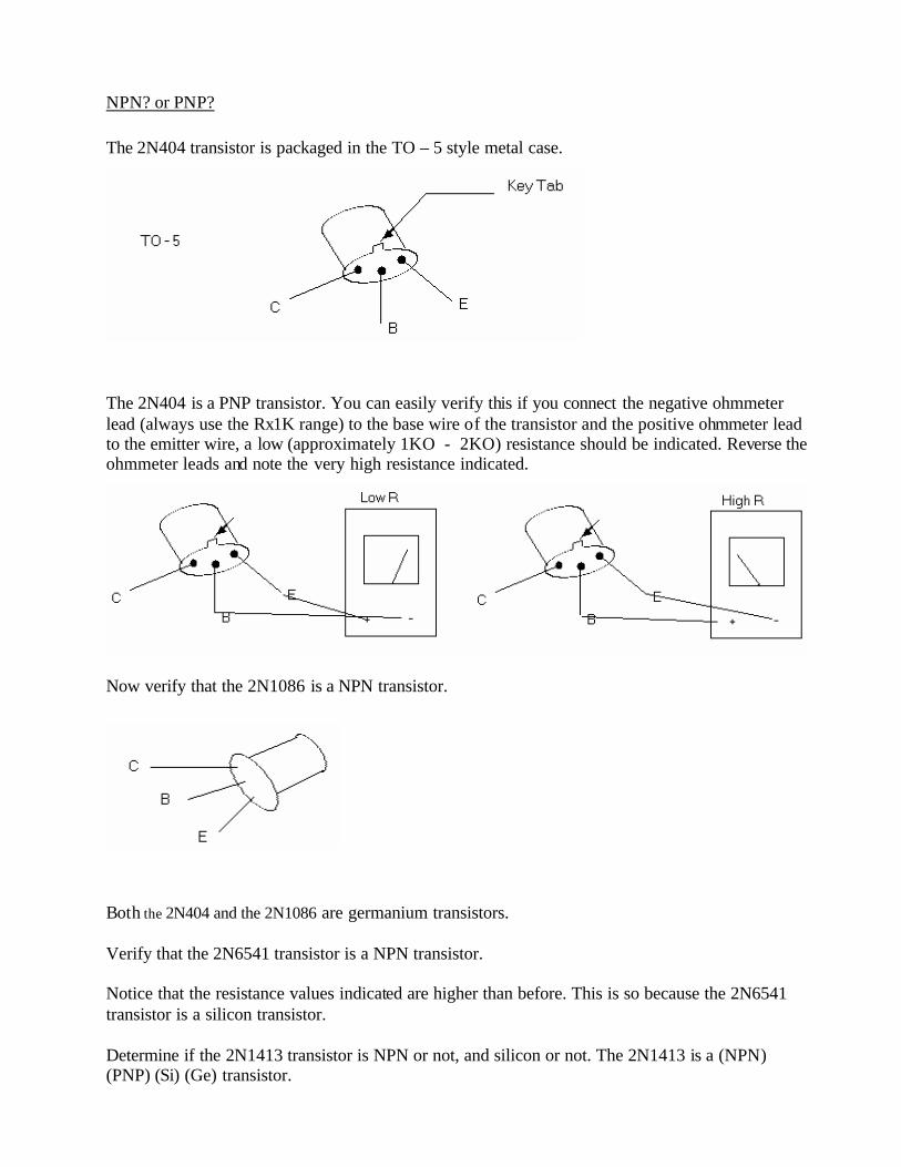
NPN? or PNP? The 2N404 transistor is packaged in the TO – 5 style metal case.
The 2N404 is a PNP transistor. You can easily verify this if you connect the negative ohmmeter lead (always use the Rx1K range) to the base wire of the transistor and the positive ohmmeter lead to the emitter wire, a low (approximately 1KO - 2KO) resistance should be indicated. Reverse the ohmmeter leads and note the very high resistance indicated.
Now verify that the 2N1086 is a NPN transistor.
Both the 2N404 and the 2N1086 are germanium transistors. Verify that the 2N6541 transistor is a NPN transistor. Notice that the resistance values indicated are higher than before. This is so because the 2N6541 transistor is a silicon transistor. Determine if the 2N1413 transistor is NPN or not, and silicon or not. The 2N1413 is a (NPN) (PNP) (Si) (Ge) transistor.
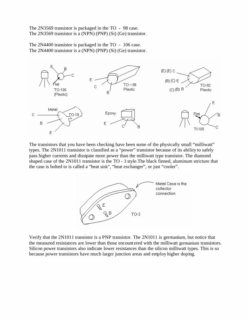
The 2N3569 transistor is packaged in the TO - 98 case. The 2N3569 transistor is a (NPN) (PNP) (Si) (Ge) transistor. The 2N4400 transistor is packaged in the TO - 106 case. The 2N4400 transistor is a (NPN) (PNP) (Si) (Ge) transistor.
The transistors that you have been checking have been some of the physically small “milliwatt” types. The 2N1011 transistor is classified as a “power” transistor because of its ability to safely pass higher currents and dissipate more power than the milliwatt type transistor. The diamond shaped case of the 2N1011 transistor is the TO - 3 style.The black finned, aluminum stricture that the case is bolted to is called a “heat sink”, “heat exchanger”, or just “cooler”.
Verify that the 2N1011 transistor is a PNP transistor. The 2N1011 is germanium, but notice that the measured resistances are lower than those encountered with the milliwatt germanium transistors. Silicon power transistors also indicate lower resistances than the silicon milliwatt types. This is so because power transistors have much larger junction areas and employ higher doping.
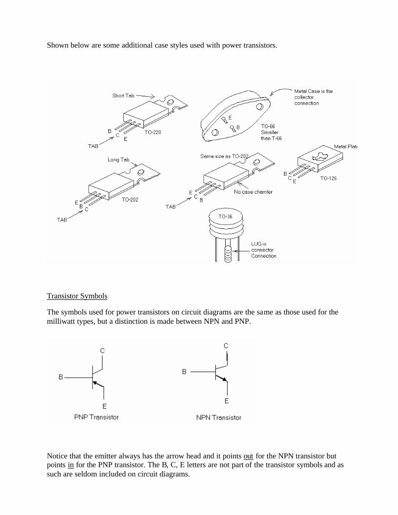
Shown below are some additional case styles used with power transistors.
Transistor Symbols The symbols used for power transistors on circuit diagrams are the same as those used for the milliwatt types, but a distinction is made between NPN and PNP.
Notice that the emitter always has the arrow head and it points out for the NPN transistor but points in for the PNP transistor. The B, C, E letters are not part of the transistor symbols and as such are seldom included on circuit diagrams.

Transistors Biasing One of the most common biasing arrangements employs a single battery or power supply. Transistors are normally biased so that the emitter junction is forward biased and the collector junction is reverse biased. In order to achieve this, a resistor voltage divider is used with the power supply or battery.
Notice that the voltage drop polarities across the upper resistors are for proper reverse biasing the collector junctions, while the lower resistor produce forward bias polarities for the emitter junctions. Sometimes the lower resistors are not used and the forward biased emitter junctions act as the lower elements in the voltage divider.
One would expect because the collector junction is reversed biased that the collector current would be very small, “transistor action”, the collector flow is usually quite large compared to the base current.

The transistor acts like a valve for electrons flowing between the collector and the emitter. A small base current, which acts like a control current, produces a much larger (sometimes hundreds of times larger) collector flow. The flow in the emitter is the sum of the base and collector flows.
Using the 2N404 transistor connect the circuit shown below.
Notice that the collector current (Ic) is far from zero and is in fact much larger than the current flowing in the ‘case lead. Questions
1. Operationally, what would be the consequence of making the base section of a transistor much. too wide?
2. Why do you suppose the maximum reverse voltage rating for the emitter junction of a
transistor is much lower than that of the collector junction?
3. Why do you suppose the collector junction gets hotter than the emitter junction in a properly biased trans istor?
4. Do you think that two diodes could be wired together as shown below to make a transistor? Explain.
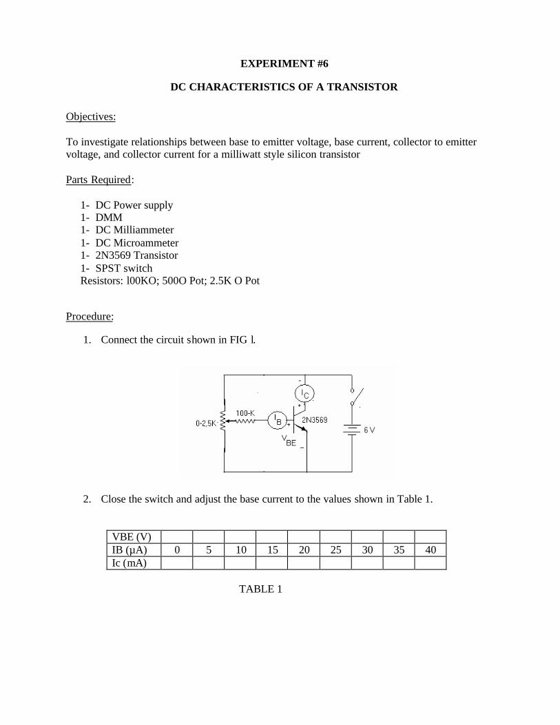
EXPERIMENT #6
DC CHARACTERISTICS OF A TRANSISTOR Objectives: To investigate relationships between base to emitter voltage, base current, collector to emitter voltage, and collector current for a milliwatt style silicon transistor Parts Required: 1- DC Power supply 1- DMM 1- DC Milliammeter 1- DC Microammeter 1- 2N3569 Transistor 1- SPST switch Resistors: l00KO; 500O Pot; 2.5K O Pot Procedure:
1. Connect the circuit shown in FIG l.
2. Close the switch and adjust the base current to the values shown in Table 1.
VBE (V) IB (µA) 0 5 10 15 20 25 30 35 40 Ic (mA)
TABLE 1

3. Modify the circuit to that shown in Fig.2.
4. Close the switch and adjust the base current to 10 microamps. Adjust the collector to emitter voltage to the values shown in table 2 and record the collector currents. Repeat for the other base currents shown in Table 2.
Vce (Volts)
IB (µA) 0 1 2 3 4 5
10 20 30 40
5. Make three graphs of the data in table 1. Examples:
6. Make a family type graph of the data in table 2. Title the graph “Step 4”. Example:
7. On your graph of step 4 draw the collector DC load lines for resistors of 470O, 1KO, and 2.2KO. Use Vcc = 5V.
8. Indicate the operating points on your load lines when IB = 30µA.
Question: 1. Which has the greater effect on Ic, changing the IB values or changing the Vce Values?
TABLE 2 Collector Currents (mA)
