electronics division internal report no. 255 - · pdf file · 2010-09-14electronics...
TRANSCRIPT

NATIONAL RADIO ASTRONOMY OBSERVATORY
CHARLOTTESVILLE, VIRGINIA
ELECTRONICS DIVISION INTERNAL REPORT No. 255
A SYNTHESIZED, 90 120 GHz SIGNAL SOURCE
J. W. ARCHER AND M. J. CRAWFORD,
DECEMBER 1984
NUMBER OF COPIES: 150
A SYNTHESIZED 90-120 GHZ SIGNAL SOURCE
J. W. Archer and M. J. Crawford, Jr.
Table of Contents
I. Introduction . . . . . . • • • • • • • • • 0 • • • • • • • • 1SII. The 26.5-40 GHz Frequency Synthesizer . . . 2 . . . . . . . . ... . . 2
A. General Description . . . . • .. . • • • • • • • • • • • • • 2B. Design of the UHF Synthesizers . . . . . • . . . . . . * • . 5C. The Coarse Tuning and Bias Modulation Amplifiers • • • • • . 11D. The Main 26.5-40 GHz Phase Lock Loop • • • • • • • • • . 14
III. The 90-120 GHz Frequency Tripler . . • • • • • • • • • • • • • .7
21IV. The Complete Synthesized LO Source . • • • • • • • • •. . . . . 2V. Summary . . . • • • • • • • • • • • • 41 • • • • • • • • • . . 27VI. Acknowledgements . . • • • • • • • • • • 0 • 0 • • • •. . . . . 28
Figures
Figure 1 26.5-40 GHz Synthesizer Block Diagram . . • • • • • 3Figure 2 0.88-1.32 GHz Synthesizer Schematic . . • •• • • • • 7Figure 3 ROM and 9's Complement Encoder SchematicFigure 4(a)
(d)
Spectrum of 1.76-2.64 GHz Synthesizer Output• 9
Spectrum of 1.76-2.64 GHz Synthesizer Output • • •
.• • • . . 10
400-500 MHz Reference Signal Spectrum . .
.I.F. Spectrum in Main Loop . . • • . • • •
•
• • • • •• •.
•
. . . 12
:Figure 5
c
Tuning Coil Driver Schematic . • • • • ••••••
(b) 0(c) 51 . 14
Figure 6 Harmonic Mixer Triplexer Schematic . • • * • • • • •Figure 7 Sweep Generator Schemati . . • . . • • . . • • •. . . 18Figure 8 FM Coil Driver and Loop Amplifier Schematic • • • •
Figure 10. . . .ripler .
• • •
!!
Figure 9(b) Tripler Block: Cross-Sectional ViewOutput Power vs Output Frequency for T
Figure 11 Tripler Conversion Efficiency vs Input Power
. . 23Figure 9(a) Tripler Block: Cross-Sectional View . • • * • • • •
Alone and for Complete Signal Source . • . . .. . 26• . .
References . • • • • • • • • • • • • • • • • •• • • • . . • . 29

A SYNTHESIZED 90-120 GHZ SIGNAL SOURCE
J. W. Archer and M. J. Crawford, Jr.
I. Introduction
The advantages of all-solid-state millimeter wavelength receivers have
been clear to system designers for many years. Substantial savings in cost
and weight, and significantly enhanced system reliability, can be achieved with
a completely solid-state design. Until recently, achieving a widely tuneable
solid-state local oscillator system has proven to be a significant obstacle
to the development of broadband heterodyne receiver systems of this type.
Developments in millimeter wave harmonic generator design [1],[2] Gunn oscillator
technology [1],[3] and the reduction in the LO power requirements for heterodyne
receivers through the use of improved, cooled Schottky diode [4] [5] or super-
conducting mixer [6],[71 elements have now made it feasible to realise practical
receivers with solid state LO's. In many applications, frequency and/or phase
stability of the LO source is of prime importance. The construction of a highly
stable, widely tuneable synthesizer [8], such as described here, is therefore
a significant development.
The following sections of this paper will describe the design and construction
of the 26.5-40 GHz frequency synthesizer. Performance data will be given, which
illustrate the frequency stability, output power and spectral purity of the
phase locked source. The design of the frequency tripler is then described
and performance curves are given. Finally, data is presented showing the performance
of the complete synthesized LO source.

II. The 26.5-40 GHz Frequency Synthesizer
A. General Description:
The principal millimeter wavelength signal source in the LO system is a
YIG tuned GaAs Gunn oscillator manufactured by Watkins Johnson, Inc. (Model
WJ-5610-302F). This oscillator may be electronically tuned between 26.5 and
40 GHz by varying the magnetic field applied to a spherical YIG resonator to
which the Gunn diode is coupled. The magnetic field is produced by current
flowing in the coils of an electromagnet, whose pole pieces enclose the YIG
element. As the tuning coil current is varied linearly from 660 mA to 1015
mA, the oscillator frequency varies in a smooth, almost linear response from
26.5 to 40 GHz. The peak deviation from linearity is about -60 MHz near the
upper and lower tuning limits. The tuning coil resistance is about 10 ohm
with an inductance of 160 mH. Another electromagnetic circuit is provided to
enable fine tuning of the oscillator frequency. This coil gives a sensitivity
of 125 kHz/mA with a maximum current of + 800 mA, resulting in a peak attainable
deviation of + 100 MHz. In order to achieve the flattest output power response
as the output frequency is varied, the supply voltage to the Gunn diode must
be changed linearly and in synchronism with the tuning coil current - at 26.5
GHz the optimum Gunn bias is 5.2 volts and at 40 GHz the optimum bias is 3.4
volts. When the bias voltage is controlled in this manner, the output power
over the full tuning range is +13 dBm + 1 dB.
Figure 1 a block diagram of the 26.5 to 40 GHz synthesizer system, shows
how the YIG tuned oscillator is incorporated into the phase lock system. The
coarse tuning coil current and Gunn diode bias are derived by digital to analog
conversion of the BCD-encoded frequency select input, so that the initial oscillator
frequency is set as near as possible to the desired output frequency. An automatic

CO
ARSE
TU
NE
D/A
CO
NV
VCO
AVAN
TEK 8
040
4.--O
UAD
HYBRID
TU
NIN
G C
OIL
DRIV
ERPH
ASE
DET
ftM
CL-
ZFM
410
MH
Z XCO
YIG
OSC
ILLA
TO
RW
J-5610-3
02F
F4 C
OIL
DRIV
ERLO
CK
IND
ICATO
R
Vis.
..PW
R A
MP
MCL-
ZFL
2000
LOO
P" F
ILTE
R
9'S
CO
MP &
SU
BT 4
9'S C
OM
P-1
0DB
BPF
450/1
00
PWR D
IV
SW
EE
PO
SC
EM
F V
T0-4
B
LOO
P FI
LTER
MO
D A
MP
BPF
2200/8
00
LIM
AM
PW
J-CLA
7
ISO
LATO
R-4
oTRIP
LEXER
BPF 2
200/8
00
10D
BCO
UPL
ERPW
R D
IVBP
F450/1
00
20D
B C
OU
PLER
•I'v ill7
if1
LPF
500
IF A
MP
HARM
ON
IC M
IXER
WJ-
6200618
HP-1
1517A
-10D
B
DC B
IAS
IN26.5
-40 G
HZ
OU
T
-10D
B
LIM
AM
PIN
J -CLA
7•
IF M
ON
ITO
R
4--P
WR D
IVLO
OP
FILT
ER
Fig
. 1
. A
blo
ck d
iag
ram
of
the
com
ple
te 2
6.5
-40
GH
z sy
nth
esiz
er s
yst
em.
A d
etai
led
des
crip
tion o
f th
e b
lock
dia
gra
m i
s g
iven
in
th
e te
xt,
alo
ng w
ith i
nfo
rmat
ion
on
th
e d
esig
n a
nd
op
erat
ion
of
the
ind
ivid
ual
sy
stem
buil
din
g b
lock
s.
fine frequency sweep signal can be injected at the input of the coarse tuning
coil bias amplifier in order to tune the oscillator close enough to the desired
frequency for lock acquisition. The microwave output from the YIG oscillator
is fed through a broadband waveguide isolator and then sampled by a 20 dB cross-
guide coupler. The sampled signal is fed to a harmonic mixer (Hewlett-Packard
Model 11517A) where it is mixed with the 15th harmonic of a 1.76-2.64 Gilt reference
signal. This signal is generated by extracting the second harmonic of the output
of one of two UHF frequency synthesizers in the system, both of which are locked
to a common, highly stable, 10 MHz reference signal. The frequency of the 2 GHz
reference is controlled by the first three digits of the frequency select input
data. Decimal 4 is subtracted from this number to correct for the 400 MHz offset
of the IF reference synthesizer and its 9's complement code generated, in order
to derive the required preset data to determine the division modulus for the
programmable divider in the UHF synthesizer. A numerical example will help
in understanding the relationships:
Let the selected frequency be 3j 543 1 GHz (no special significance).
The division modulus will be 316 - 11 = 312. The output frequency from the UHF
synthesizer will be (10 MHz/12) x 312 x ii = 1040 MHz. Its second harmonic component,
which is fed to the harmonic mixer, will be 2080 MHz. When the YIG oscillator
is tuned to the desired frequency, the IF output frequency from the harmonic
mixer will be 31,654.3 - 15 x 20 80 = 454.3 MHz.
The IF output from the harmonic mixer is amplified and fed to a phase detector
where it is correlated with a signal derived from the second UHF synthesizer.
The frequency of the ssoond synthesizer is controlled by the remaining three
digits of the frequency select command and incorporates a fixed frequency offset
of 1100 MHz. Thus, in the example above the output frequency would be

400 + 54.3 = 454.3 MHz, which is exactly the required frequency if the YIG tuned
oscillator is to lock at 31.6543 GHz. The output of the phase detector is filtered,
amplified and fed back to control the phase of the YIG oscillator via the bias
applied to the fine tuning (FM) coil.
The use of separate synthesizers for coarse and fine control of the reference
frequencies is essential if acceptable phase noise is to be achieved in the
spectrum of the locked millimeter wave oscillator. The phase noise of the output
signal, within a loop bandwidth separation from the carrier, will be determined
primarily by the phase noise characteristics of the harmonic mixer reference
signal. If only the 1.76-2.64 GHz reference is made variable and the other
reference is fixed at, say, 400 MHz, it would be necessary to operate the phase
detector at 833 Hz in the remaining synthesizer to achieve a 100 KHz increment
in the millimeter wave output signal. Since the carrier-to-noise ratio for
phase noise degrades as the square of the frequency ratio, the FM noise
characteristics of the primary reference oscillator would be degraded by about
70 dB in the final output spectrum - clearly an unacceptable situation for practical
oscillators. By controlling the frequency of both reference signals and carrying
out fine frequency adjustment using an IF frequency offset, the phase noise
degradation is reduced to about 40 dB, which is acceptable when a high quality
10 MHz reference oscillator is employed.
B. Design of the UHF Synthesizers:
The 1.76-2.64 GHz and 400-500 MHz synthesizers are very similar in design,
using essentially the same digital circuitry for prescaling, variable modulus
division and phase/frequency detection. The significant differences are the
different reference frequencies (833 kHz vs 25 kHz), the number of variable
modulus counter stages (3 vs 4) and the manner in which the frequency select
5
digits are derived. Because of the similarities, only the 1 .76-2.64 GHz synthesizer
circuit will be described in detail.
In this case, because of the technological constraints on prescaler performance,
the phase lock loop operates at half the desired output frequency, i.e.,
0.88-1.32 GHz. The oscillator employed is a varactor tuned transistor oscillator
(EMF VT0-JIB) which provides more than +13 dBm over the fundamental frequency
range and -25 dBm + 2 dB at the second harmonic. The output from the oscillator
is split by a 3 dB power divider. One output from the divider is further attenuated
by 10 dB and fed to a divide by 4, ECL prescaler. The other output is passed
through a bandpass filter, which passes the desired second harmonic component
but rejects the fundamental and other higher order harmonics from the oscillator.
The filter output is fed to a variable gain, broadband power amplifier chain
with a total maximum gain of 40 dB, boosting the signal power to a nominal maximum
of +15 dBm. A second identical bandpass filter follows, before the reference
signal is coupled to the harmonic mixer. The second filter prevents noise from
the power amplifiers reaching the high gain, low noise IF chain of the millimeter
wave phase lock loop.
The fixed modulus, divide by 4, ECL prescaler (Plessey SP8611B) at the
input of the digital divider chain is followed, as shown in Figure 2, by a dual
modulus (+10/ill) ECL counter (11C90). This counter is interconnected with
a series of synchronously clocked, presetable high speed TTL BCD decade counters
(70160) to implement a variable modulus counter using pulse swallowing techniques
[9]. The use of the Schmitt trigger (74S14) to generate the synchronous clock
signal for the 74E 1 160 counters helps eliminate false clocking problems encountered
at the higher input frequencies. Printed circuit, 50 ohm microstriplines are
used to couple the high frequency signals to the 5P6611B and 11C90 counters.

0-10
K1.
0
+50
TO
I.
VA R
ACTO
RM
OuN
1N91
424
0 pF
-15
7-30
p F
0.0
1
0.01
330
0-10
K12
1.0
1204
00 D
ET
741
4-
—15
IN 5
14
LOCK
10
K5
V-}
1 N
D1CA
TOR
2Z
EN
ER
41
51N
914
741
10K
741 47
0K470K
110
ISO
620
+5
110
10 3 3
03
620
■■•••■
.
0 4
1 4 I
3 1
12
17
*12 D
EC
CT
R 9
.31
415
F1G
015
1041
110
2014
F 16
0 D
EC C
TR
1312
15 1 9
LSD
MS
D
9s C
OM
PLE
ME
NT
OF
BC
D
464 4
Fig
. 2 .
A d
etai
led c
irtu
it d
iag
ram
of
the
0.8
8-1
.32
GH
z d
igit
al f
requen
cy s
ynth
esiz
er.
The
1.7
6-2.
64 G
Hz
refe
renc
e si
gnal
fed
to
the
mil
lim
eter
wav
e ha
rmon
ic m
ixer
is
obta
ined
by
filt
erin
g an
d am
plif
ying
the
sec
ond
harm
onic
of
the
VC
O o
utpu
t si
gnal
.

The coupling and bypass capacitors are chip capacitors. The bypass capacitors
are grounded to the ground plane of the board using low inductance, plated-through
holes.
The division modulus preset digits to the programmable counters are derived
using 9's complement encoders, one channel is illustrated in Figure 3. The
subtract decimal 4 function is performed prior to 9's complement encoding using
a look-up table stored in a set of read only memories. The complete circuit
and table are given in Figure 3. The output signal from the programmable divider
is fed, via a level translating resistor network, to an ECL phase frequency
detector (12040). The 833 kHz reference input for the detector is derived from
the 10 MHz standard using a divide by twelve, 74LS92 counter. The output pulses
from the phase detector are coupled to an active second order loop filter/integrator
with adjustable damping controls. An AM-464 (Analog Devices) operational amplifier
is used, which is capable of handling the high voltages required to directly
bias the tuning varactor in the VCO for complete coverage of the oscillator
tuning range. A common problem with a loop of this type is the appearance of
spurious components in the spectrum of the locked oscillator spaced at harmonics
of 833 kHz from the desired output frequency. These arise because of insufficient
filtering of the sharp output pulses from the phase/frequency detector at the
varactor bias output. In the present design, with a loop natural frequency
of about 20 kHz [10], RC pulse prefiltering (0.01 g capacitors in the input
resistor network) and a series resonant LC trap at the op-amp output are used
to reduce the amplitude of the spurious signals to acceptable levels. Photographs
of the typical output spectrum (at 2 GHz) from the 1.76-2.64 Grit synthesizer,
shown in Figures 4(a) and 4(b), demonstrate that the unwanted components are
at least 60 dB below the carrier. A simple lock indicator circuit is implemented
8

1st
10 I■11
LSD
0 4I •
VD
.11
BCD
13
6331
-1
12
6331
.1
134
131515
1 O
.10
MSD
L D
CO
-
BCD
-49'
s C
OM
PLE
ME
NT
OF
BC
D
SU
BT
RA
CT
4 P
RO
M T
AB
LE
Hex
Add
ress
LSD
RO
MO
ther
Tw
o R
OM
S's
B 8
4 2
1B
8 4
2 1
3 4
1312
6331
-1
43
en■
Fig
. 3.
3. A
dia
gra
m s
how
ing t
he
des
ign
of
the
EtT
subtr
act
four,
RO
M c
ircu
it a
nd t
he
BC
D t
o "
9's
com
plem
ent o
f B
CD
"co
nv
ert
er.
Th
e i
nse
t ta
ble
giv
es
the l
ogic
use
d i
nim
ple
men
tin
g t
he
loo
k-u
p t
able
sto
red i
n R
OM
.
11
00
1 0
11
11
11 1 000
0 1
11 0
21
01
11
0 1
10
13
10
1 1
00 1
1 0
00
11
11
01
01
15
01 1 10
0 1
0 1
06
01 101
0 1
0 0
17
01 1
00
0 1
0 0
00
10
1 1
0 0
11
10 1
0 1
00 0
1 1
0OA O
F 101 0
11
011
01
11
112
0 1
11 0
130
11
0 1
140 1
1 0
015
0 1
0 1
116
0 1
0 1
017
0 1
0 0
118
0 1
0 0
019
0 0
11
1

Ai*
a) The 1.76-2.64 GHz reference signal to the harmonicmixer - set at 2.0 GHz. Analyzer B.W. = 3 KHz,horizontal scale = 20 KHz/div, vertical scale = 10 dB/div.
As for a) but with horizontal scale = 500 KHz/div.
Fig. 4. Photographs of typical signal spectra at importantmonitor points in the synthesizer system.
10
using a differential amplifier to detect the presence of a frequency correction
signal from the 12040 followed by a dual threshold comparator which gives a
5 volt output signal when the loop is unlocked.
Figure 4(c) shows the typical output spectrum from the 400-500 MHz synthesizer.
The VCO used in this phase locked loop is an Avantek 8040 varactor tuned device.
A bandpass filter is required between oscillator and prescaler to eliminate
false triggering of the divider due to the second harmonic component at the
output of the VCO. In this loop, four 74F160 counters are used to implement
the variable modulus counter, but the most significant digit is fixed at a count
of 4. The code for the 3 remaining digits is a 9 1 8 complement encoded version
of the last three digits of the frequency select command input.
C. se
Figure 5 gives a schematic diagram of the coarse tuning coil current driver
and Gunn diode bias modulator. A pair of three digit BCD, digital-to-analog
converters are used to generate an analog voltage from the BCD frequency select
input. The resultant tuning voltage at the output of the summing amplifier
A is equal to the selected frequency in GHz divided by 10. This voltage drives
a linear voltage to current converter (op-amp B and ECG261 transistor) whose
gain and offset can be adjusted so that the YIG tuned oscillator frequency is
as close as possible to the desired locking frequency. Coil current is sensed
by a precision 1 ohm resistor in series with the windings. The output voltage
from amplifier A is also used to control the bias voltage applied to the Gunn
diode in order to minimize the variations in YIG oscillator output power with
operating frequency. The voltage from amplifier A is fed to non-inverting amplifier
C, which has a voltage gain of 3.3 and includes an adjustable offset control.
The output from this amplifier is fed via a 14.3K resistor to the control input
11
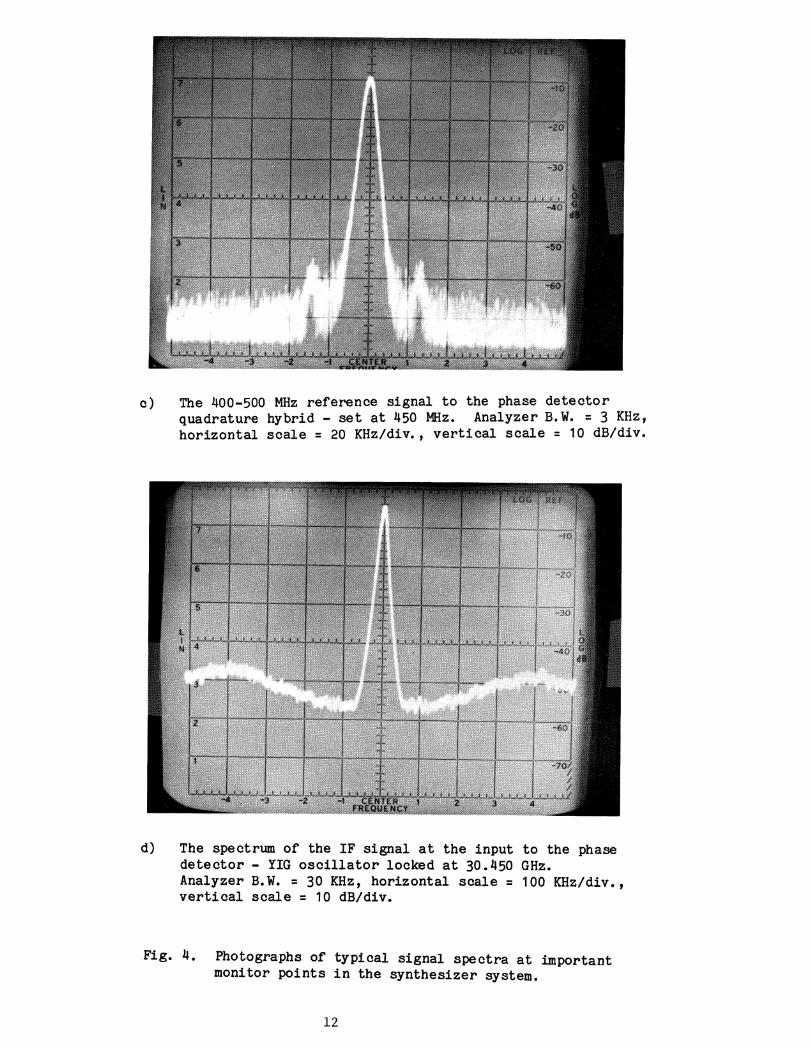
a) The 400-500 MHz reference signal to the phase detectorquadrature hybrid - set at 450 MHz. Analyzer B.W. = 3 KHz,horizontal scale = 20 KHz/div., vertical scale = 10 dB/div.
The spectrum of the IF signal at the input to the phasedetector - YIG oscillator locked at 30.450 GHz.Analyzer B.W. = 30 KHz, horizontal scale = 100 KHz/div.,vertical scale = 10 dB/div.
Fig. 4. Photographs of typical signal spectra at importantmonitor points in the synthesizer system.

+17
100K 5
0K 1
00K
+15
-15
0I.
IK
IK
ECG
261
+15 •
(10
K
+15
-15
1 22
14 1
5N
W)
8_16.
1° f
t11
1914
210
KTO
TU
NIN
G C
OIL
(.6
3 —
WI
A)
10K
IOW
+15(A
)
• 15
A R
I
---1
2
21 2
71
6=
10K
0-1
5I Or7,
5K
GsK
10K
'""0.
01BC
D
COD
E30 K
0.01
2115
19—
— 00 2
2 X
1N11
861 2
A
14, K
TO GU
NN
DIO
DE
10K
02
•N
•El t
7I
470K
2 14
9-15
1N91
410
K
+15
10K
+15
Fig
. 5 . A
schem
atic d
iagra
m o
f th
e c
oars
e t
unin
g c
oil d
river
circuit s
how
ing
the D
/A c
onvert
er,
driver
am
plifier
and G
unn d
iode b
ias m
odula
tor.
of a current controllable, positive 1 amp voltage regulator (LAS15U). The
sensitivity of the inverting control input is set by a variable 10K feedback
potentiometer connected between the regulator output and ground. By suitably
adjusting the gain and offset controls, the Gunn bias voltage can be made to
vary linearly from 5.2 to 3.6 volts as the tuning voltage varies from 2.65 to
4.0 volts. The 1N1186 diodes connected between the Gunn diode and the regulator
provide a constant voltage drop of 1.2 volts, allowing the LAS15U to operate
at output voltages between 6.8 and 4.8 volts, which are above its minimum output
voltage limit of 4.0 volts. The zener diode and fuse protect the Gunn diode
against overvoltage conditions that might occur in the event of failure of the
regulator or other circuit element.
Op-amp D, connected as a comparator, is used to prevent an incorrect input
code from causing the application of an excessive bias voltage to the Gunn
oscillator. Should a BCD input number be selected which is less than 26.5 GHz,
the comparator output swings positive, forcing the tuning voltage to remain
constant at 2.65 volts. If the selected frequency is above 40 GHz, then the
Gunn voltage will be below 3.5 volts and the tuning coil current is limited
to a safe value of less than 1.5 amps by the internal resistance of the windings.
D.
As described previously, a ample of the YIG tuned oscillator output is
fed to a Hewlett Packard harmonic mixer where it is mixed with the 15th harmonic
of a reference signal in the range 1.76-2.64 GHz. The reference signal, mixer
bias and IF output signal are coupled to and from the single coaxial port of
the mixer using a triplexing filter shown schematically in Figure 6. The triplexer
is comprised of a pair of three-element, lowpass filters which isolate the hie)
power, 2 GHz reference signal from the 450 MHz IF amplifiers, and both of these
111

4-8
41
5555
TIM
ER
•I
61
23
0 3
FM
CO
IL
10 O
K
I O
K
741
0.01
16II
I14
512
193
BIN
CTR
13
KIM
111E
11 E
MIE
MI
193
11 12
31
3K
11
11311111E
1111111111111E
111
1211
110
19 1
8 1
76
1 5
:
15A
DO
8
16D
AC
13_
141
4_
2
-15
TU
NIN
GN
ov,—
>C
OIL
SW
EE
P7,
5MO
FF
SE
T
Fig
. 6
. A
dia
gra
m s
how
ing t
he
pri
nci
pal
fea
ture
s o
f th
e h
arm
on
ic m
ixer
sig
nal
tri
ple
xer
. T
he
dia
gra
mal
so s
ho
ws
the
auto
mat
ic l
evel
co
ntr
ol
syst
em w
hic
h a
dju
sts
the
pow
er l
evel
of
the
1.7
6-2
.61 1
GH2
sig
nal
to
mai
nta
in a
co
nst
ant
bia
s cu
rren
t in
th
e h
arm
on
ic m
ixer
dio
de.

signals in turn from the mixer DC bias input. DC blocking capacitors are provided
at the RF and IF ports. The triplexing filter was fabricated using microstripline
techniques on aluminum-backed, Teflon fiberglass dielectric material.
The harmonic mixer, which has widely varying sensitivity over the range
1.76-2.64 GHz, is operated in a zero voltage bias mode at a constant forward
current of 4.8 mA. The bias current is held constant by adjusting the power
of the 2 GHz input using a servo loop (S11010, in Figure 6), which controls the
gain of the reference signal power amplifier. Operation at a constant bias
current ensures a more uniform sensitivity for the harmonic mixer between 26.5
and 40 Gliz and reduces variations in the IF power at the phase detector.
The 400-500 MHz IF output from the triplexer is passed to a lowpass filter
(500 MHz cutoff), which further attenuates the 2 GHz reference signal, before
being fed to a low noise, high gain amplifier (3 dB NF, 45 dB gain). The first
amplifier is followed by a 400-500 MHz bandpass filter, a monitor directional
coupler, a limiting amplifier and a 10 dB attenuator, resulting in a nominal
input power to the phase detector power divider of +3 dBm. The reference signals
for the two double balanced mixer phase detectors are derived from the amplified
400-500 MHz synthesizer output using a quadrature hybrid. Nominal input power
to the hybrid is +3 dBm.
In order for the loop to be able to acquire lock, the difference frequency
between the IF signal from the harmonic mixer and the phase detector reference
signal must be less than the bandwidth of the loop filter (about 500 KHz).
This will not be the case when the YIG oscillator frequency is preset by the
coarse tuning coil because of the deviation of the tuning current vs frequency
response from linearity. Nevertheless, the difference frequency should be less
than 60 MHz for the oscillator used here. Provision is made in the design of
the coarse tuning coil driver amplifier for the injection of a small sweep offset
voltage which can be used to bring the YIG oscillator frequency within the
lock range of the loop.
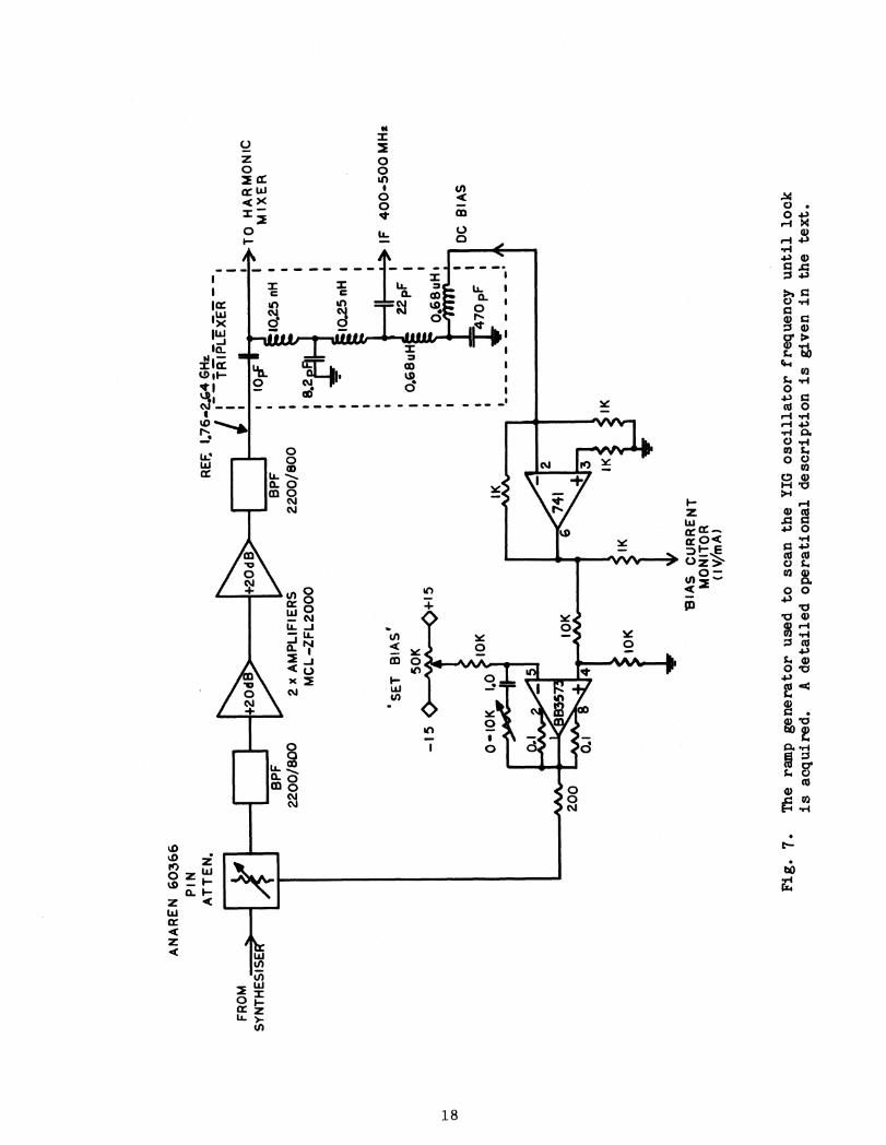
The sweep circuit is illustrated in Figure 7. The sweep function is implemented
digitally, a technique which has significant advantages over an analog method.
A 256 Hz clock pulse generated by a 555 timer is fed via a control gate to a
cascade of two 741,8193 binary up/down counters. The counter outputs are coupled
to an eight-bit D/A converter, which generates a repetitive voltage ramp as
the counters are clocked. The voltage ramp is fed via an appropriate scaling
resistor to the input of the coarse tuning coil driver amplifier, resulting
in a modulation of the YIG oscillator frequency by about + 100 MHz in synchronism
with the sweep voltage. When the YIG oscillator frequency comes within the
capture range of the loop (about 1 MHz) and lock is acquired, a voltage comparator
connected to the output of the quadrature phase detector senses the locked condition
and generates a +5 volt signal which disables the clock to the sweep counters.
The coarse tuning bias is thus latched at the condition at which lock was acquired.
A problem that has been encountered with the YIG oscillator used here is
significant frequency vs temperature dependence. In operation, after the loop
is locked, ambient temperature Changes can cause the oscillator to drift out
of the range of the loop correction signal. A simple addition to the sweep
circuit has enabled this problem to be overcome. As shown in Figure 7, the
current in the YIG oscillator FM coil is converted to a suitable proportional
voltage and sensed by a dual threshold comparator with hysteresis which is
triggered should the correction voltage exceed + 2 volts (available range is
+ 4 volts at a sensitivity of 0.1V/A). The comparator outputs control gates
which feed the clock signals to the up or down clock inputs of the binary counter
1 7
2 x
AMPL
IFIE
RSM
CL—
ZFL2
000
BPF
2200
/800
BPF
2200
/800
200
10K
0 • 1
0K 1
.0SET
BIAS'
50K
—15
•+1
5
IK AAA,
0.68
uH
10.2
5 nH 1-
4+
1F
400
4.50
0 M
Hz
22 F p.
0.68
uH
;470 p
FD
C B
IAS
0.1
1KIK
10K
WO
4W
D 4W
D O
W 4•111 4W
D oa
r W
O 4
WD
4W
D •
10K
I K
FROM
SYNT
HESI
SE
GHz
TR I
PLEX
ER
'OFF
'>
OwA
H IA X
R EM R
ON IC
1025
nH
1 1
821
ANAR
EN 6
0366
PIN
AT T
EN.
REF,
BIAS
CU
RREN
TM
ONI
TOR
1 Vim
A)
Fig
. 7. T
he r
amp
gene
rato
r us
ed t
o sc
an t
he Y
IG o
scil
lato
r fr
eque
ncy
unti
l lo
ckis
acq
uir
ed.
A d
etai
led o
per
atio
nal
des
crip
tion i
s g
iven
in
th
e te
xt.
cascade: If the FM coil current exceeds the threshold level, the clock is applied
to the counters in such a way as to change the coarse tuning voltage to result
in a reduction of FM coil current magnitude. A 0.5 volt hysteresis for the
comparator thresholds provides an overcorrection safety margin.
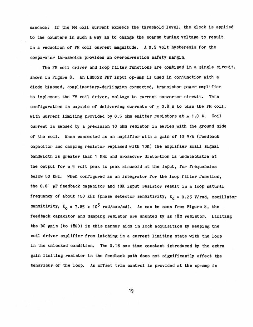
The FM coil driver and loop filter functions are combined in a single circuit,
shown in Figure 8. An LH0022 FET input op-amp is used in conjunction with a
diode biassed, complimentary-darlington connected, transistor power amplifier
to implement the FM coil driver, voltage to current converter circuit. This
configuration is capable of delivering currents of + 0.8 A to bias the FM coil,
with current limiting provided by 0.5 ohm emitter resistors at + 1.0 A. Coil
current is sensed by a precision 10 ohm resistor in series with the ground side
of the coil. When connected as an amplifier with a gain of 10 V/A (feedback
capacitor and damping resistor replaced with 10K) the amplifier small signal
bandwidth is greater than 1 MHz and crossover distortion is undetectable at
the output for a 5 volt peak to peak sinusoid at the input, for frequencies
below 50 KHz. When configured as an integrator for the loop filter function,
the 0.01 gF feedback capacitor and 10K input resistor result in a loop natural
frequency of about 150 KHz (phase detector sensitivity, K d = 0.25 V/rad, oscillator
sensitivity, Ko = 7.85 x 10⁵ rad/sec/mA). As can be seen from Figure 8, the
feedback capacitor and damping resistor are shunted by an 18M resistor. Limiting
the DC gain (to 1800) in this manner aids in lock acquisition by keeping the
coil driver amplifier from latching in a current limiting state with the loop
in the unlocked condition. The 0.18 sec time constant introduced by the extra
gain limiting resistor in the feedback path does not significantly affect the
behaviour of the loop. An offset trim control is provided at the op-amp in
19
6
2 2K
10K
IOW
D45
C8
+15
0-10
0,01
. T
he
circ
uit
dia
gra
m o
f th
e F
M c
oil
dri
ver
am
pli
fier
whic
h i
nco
rpora
tes
the
loo
p f
ilte
r fo
r th
e Y
IG o
scil
lato
r p
has
e lo
cked
loop.
DE
TE
CT
OR
2,2K
D44
C8 0.5
IW 0,5 1W
DIO
DES
1-4
ON
CO
MM
ON
HEA
TSIN
KW
ITH
D44
/045
•T
O F
M C
OIL
• (±
o.13
A)
I 010
K
LH 10
31-
411‘
61F-
.-F
RO
MI=
PH
AS
E •
1210
K
2N 3
439
ALL
DIO
DES
IN
914
610
0
100
MM
5416
order to allow compensation for the DC offset associated with the balanced mixer
phase detector.
Figure 4(d) shows'the spectrum of the IF signal measured at the IF monitor
coupler output with the YIG oscillator phase locked at 30.4500 GHt. The spectrum
is free of spurious non-harmonically related components to at least 30 dB below
the carrier. The noise side bands characteristic of a spectrum from a phase
locked oscillator with a 3 dB loop bandwidth of about 400 KHz are clearly seen.
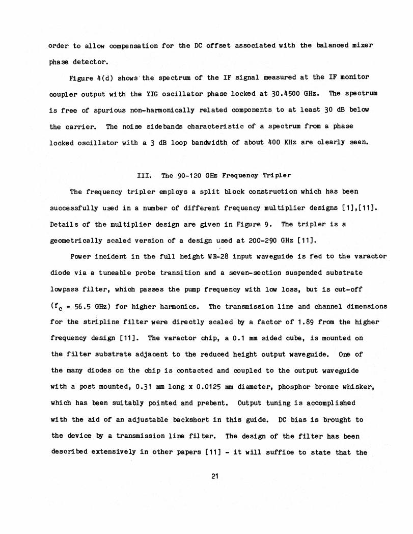
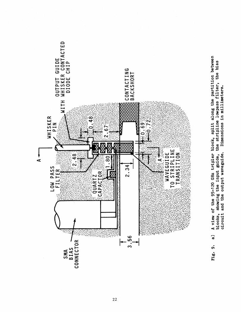
The 90-120 GHZ Frequency Tripler
The frequency tripler employs a split block construction which has been
successfully used in a number of different frequency multiplier designs [1],[11].
Details of the multiplier design are given in Figure 9. The tripler is a
geometrically scaled version of a design used at 200-290 Wiz [11].
Power incident in the full height 14111-28 input waveguide is fed to the varactor
diode via a tuneable probe transition and a seven-section suspended substrate
lowpass filter, which passes the pump frequency with low loss, but is cut-off
(fo = 56.5 GHz) for higher harmonics. The transmission line and channel dimensions
for the stripline filter were directly scaled by a factor of 1.89 from the higher
frequency design [11]. The varactor chip, a 0.1 mm sided cube, is mounted on
the filter substrate adjacent to the reduced height output wavegpide. One of
the many diodes on the chip is contacted and coupled to the output waveguide
with a post mounted, 0.31 mm long x 0.0125 mm diameter, phosphor bronze whisker,
which has been suitably pointed and prebent. Output tuning is accomplished
with the aid of an adjustable backshort in this guide. DC bias is brought to
the device by a transmission line filter. The design of the filter has been
described extensively in other papers [11] - it will suffice to state that the
21
_T_
3. 5
6CO
NTACTIN
GBACKSH
ORT
WH
ISKER
PIN
OU
TPU
T G
UID
EW
ITH
WH
ISKER C
ON
TACTED
DIO
DE C
HIP
WAVEG
UID
ETO
STRIP
LIN
ETRAN
SIT
ION
••
2.3
4
Fig
. 9. a
) A
vie
w o
f th
e 95
-120
GH
z tr
iple
r bl
ock,
spl
it a
long
the
par
titi
on b
etw
een
bloc
ks, s
how
ing
the
inpu
t gu
ide,
the
str
ipli
ne l
owpa
ss f
ilte
r, t
he b
ias
circ
uit
and
the
outp
ut w
aveg
uide
. Dim
ensi
ons
in m
illi
met
ers.

SECTIO
N A
A
**.
.0
0
C■1 C
D C
D
TRAN
SFO
RM
ER D
IMEN
SIO
NS
WH
ISKER P
IN
WAVEG
UID
ETR
AN
SFO
RM
ER
DIO
DE C
HIP
QU
ARTZ
STRIP
LIN
ESU
BST
RATE
STEP
WID
THH
EIG
HT
02.4
80.4
8
12.2
80.6
1
1.8
40.7
8
31
650.8
3
INPU
TW
AVEG
UID
E
b )
Fig
. 9.
A s
ecti
on t
hro
ugh t
he
blo
ck d
etai
ling t
he
wav
egu
ide
tran
sfor
mer
and
dio
de m
ount
ing
arra
ngem
ent.
bias line approximates a quarter-wave, short circuited stub at 50 GHz, thus
minimizing the effect of the bias circuit on the performance of the lowpass
filter near cut-off.
A quarter-wave, two section impedance transformer couples the 2.48 mm x
0.48 mm reduced height guide to the 1.66 mm x 0.83 mm output guide. Power can
flow in the wider guide at the second harmonic, whereas the output guide i
out off at this frequency. The transformer is thus used to implement a reactive
second harmonic idler termination by spacing it approximately X g/2 (at the second
harmonic wavelength) from the plane of the diode.
The varactor diode is a Schottky-barrier device fabricated by R. Mattauch
at the University of Virginia (designated 8P2) with a zero bias capacitance
of 28 fF, a DC series resistance of 10.3 ohms and a breakdown voltage of 20
volts at uA. These devices have a highly non-linear capacitance versus voltage
law which approximates the inverse half power behaviour of an ideal abrupt junction
varactor to within 5 volts of the breakdown limit.
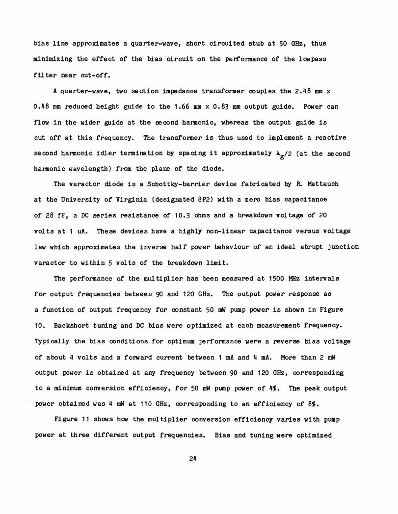
The performance of the multiplier has been measured at 1500 MHz intervals
for output frequencies between 90 and 120 GHz. The output power response as
a function of output frequency for constant 50 MW pump power is shown in Figure
10. Backshort tuning and DC bias were optimized at each measurement frequency.
Typically the bias conditions for optimum performance were a reverse bias voltage
of about 4 volts and a forward current between 1 mA and it mA. More than 2 MW
output power is obtained at any frequency between 90 and 120 GHz, corresponding
to a minimum conversion efficiency, for 50 mW pump power of 4%. The peak output
power obtained was 4 mW at 110 GHz, corresponding to an efficiency of 8%.
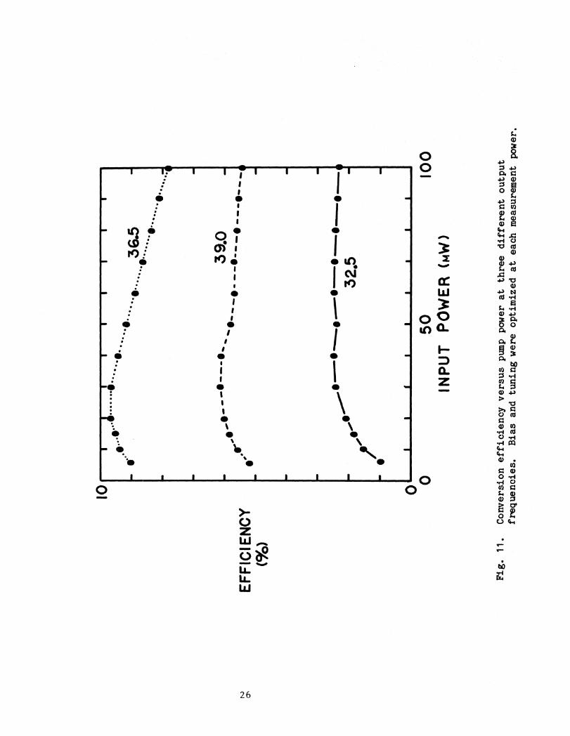
Figure 11 shows how the multiplier conversion efficiency varies with pump
power at three different output frequencies. Bias and tuning were optimized
211

x,.
• • •
iv°
XX
— X
—
\X
‘
■X°.
..4(
)(.4
W
.•••
•....
S...
...
10
OU
TPU
TPO
WER
(14 W
)
9010
512
0O
UTP
UT
FFtE
CLU
ENCY
(G
FIz)
Fig
. 10.
Outp
ut
pow
er v
ersu
s o
utp
ut
freq
uen
cy f
or
the
trip
ler:
A)
at c
onst
ant
50 m
W i
nput
pow
er (
from
a k
lyst
ron
sour
ce)
and
B)
whe
n pu
mpe
d by
the
26.5
-40
GH
z Y
IG o
scil
lato
r.F
or
curv
e A
), t
he
trip
ler
bia
s an
d t
un
ing
wer
e o
pti
miz
ed a
t ea
ch f
requen
cy,
wher
eas
for
curv
e 1
3)
the
tun
ing
was
op
tim
ized
bu
t th
e b
ias
was
fix
ed, as
des
crib
ed i
n t
he
text.
EFFIC
IEN
CY
Yo)
50
INPU
T P
OW
ER (
mW
)
Fig
. 1
1.
Co
nv
ersi
on
eff
icie
ncy
ver
sus
pu
mp
po
wer
at
thre
e dif
fere
nt
outp
ut
freq
uenc
ies.
Bia
s an
d tu
ning
wer
e op
tim
ized
at
each
mea
sure
men
t po
wer
.
for best performance at each pump level. Although the tripler can safely handle
input powers of up to 120 mW, the best conversion efficiency occurs at input
powers of about 30 mW.
IV. The Complete Synthesized LO Source
Figure 10 shows the output power response of the complete synthesized LO
system, with the tripler pumped by the phase locked, YIG-tuned Gunn oscillator.
More than 1 mW output power is available at any frequency between 90 and 120 GHz
when the tripler tuning is optimized at each operating frequency. The tripler
bias was fixed at a voltage of 3.5 volts for these measurements. The tuning
curves (position vs operating frequency) for the tripler backshorts are monotonic
and very repeatable. Motorized servo tuning of the multiplier backshorts could
easily be implemented automatically by using the frequency select input, resulting
in completely automatic operation of the synthesized local oscillator system.
V. Summary
The synthesized 90-120 GHz local oscillator system described in this paper
was designed for use with cooled Schottky diode or SIS mixer heterodyne radiometers.
The system is fully automatic in operation and exhibits adequate output power,
wide tuning range and excellent frequency stability, making it an ideal choice
for application as an LO source in millimeter-wave spectrometer receivers.
There clearly exist other areas of application for such a signal source. Some
possibilities are: i) as a phase stable local oscillator for the receivers
in a phase coherent millimeter wave antenna array, ii) as a synthesized swept
frequency signal generator for laboratory test applications. The unit described
here is to be incorporated in the near future into a 100-120 GHz SIS receiver
27

system [12] to be installed on the NRAO 12 meter diameter radio telescope near
Tucson Arizona.
VI. Acknowledgments
The authors gratefully acknowledge the assistance of N. Horner Jr. who
assembled the tripler block and G. Taylor who fabricated the tripler mount.
Prof. R. Mattauch of the University of Virginia is thanked for providing the
Schottky diodes used in the multiplier. Thanks also go to M. Balister who provided
helpful comments and advice during the construction of the synthesizer.
28
References
1. J. W. Archer, "All Solid-State Receiver for 210-2 110 GHz," IEEE Trans on
MIL , vol. MTT-30 p. 1247, August 1982.
. . R. Erickson, "A High Efficiency Frequency Tripler for 230 GHz " Proc.
12112/ar,„Ktan..2,011, (Helsinki, Finland), p. 288, Sept 1982.
J. E. Carlstrom, R. L. Plambeck and D. D. Thornton, "A 60-115 GHz Tuneable
Gunn Oscillator" submitted for publication to IEEE Traus. on MTT,
August 1984.
. C. R. Predmore N. R. Erickson, P. F. Goldsmith and J. L. R. Marrero, "A
Broadband Ultra Low-Noise Schottky Diode Mixer Receiver from 80 to
115 GHz," IZELIrana,QAM., vol. MTT-32, p. 1198, May 19811.
. 14. Archer and M. T. Faber, "A Very Low-Noise Receiver for 80 to 120
GHz, Int. J. 1.R. and MM-Wav_es vol. 5, no 8, p. 1069, August 19811.
6. S-K. Pan, M. J. Feldman, A. R. Kerr and P. Timbie, "A Low Noise 115 GHz
Receiver Using Superconducting Tunnel Junctions, h ,
vol. 43, p. 786, 1983.
7. L. R. D'Addario, "A 90-120 GHz KS Mixer Having Gain and Wide Bandwidth,"
'Qt. J. 1,R. and MM-Waves, vol. 5, no. 10, October 19811.
8. F. M. Gardner, "Phaselock Techniques", p. 208, John Wiley, New York, 1979.
9. "Pulse Swallowing Revisited," Fairchild ECL Data Book, p. 9-56/581, Fairchild
Camera and Instrument Corp., Mountain View, CA, 1977.
10. F. M. Gardner, ibid, p. 11.
11. J. W. Archer, "An Efficient 200-290 GHz Frequency Tripler Incorporating
a Novel Stripline Structure," IEEE Trans. on MTT, vol. MTT-32,
p. 1116, April 19811.
29
12. J.W. Archer, "A High Performance 2.5K Cryostat Incorporating a 100-120
GHz Dual Polarization Receiver", submitted for publication to Rev,
ad".....Ingda7,4 October 1984.
30