electronics and communication … iare institute of aeronautical engineering dundigal, hyderabad -...
TRANSCRIPT

COURTESY IARE
INSTITUTE OF AERONAUTICAL ENGINEERING
Dundigal, Hyderabad - 500 043
ELECTRONICS AND COMMUNICATION ENGINEERING
QUESTION BANK
OBJECTIVES
To meet the challenge of ensuring excellence in engineering education, the issue of quality needs
to be addressed, debated and taken forward in a systematic manner. Accreditation is the principal
means of quality assurance in higher education. The major emphasis of accreditation process is
to measure the outcomes of the program that is being accredited.
In line with this, Faculty of Institute of Aeronautical Engineering, Hyderabad has taken a lead in
incorporating philosophy of outcome based education in the process of problem solving and
career development. So, all students of the institute should understand the depth and approach of
course to be taught through this question bank, which will enhance learner’s learning process.
1. Group - A (Short Answer Questions)
UNIT - I
S. No
Questions
Blooms
Taxonomy
Level
Program
Outcome
1 Define Microprocessor and give the power supply &
clock frequency of 8085.
Knowledge 1
2 List out few applications of microprocessor-based system. Knowledge 1
3 State the difference between 8085 & 8086 microprocessor. Knowledge 1
Course Name : Microprocessors and Microcontrollers
Course Code : A60430
Class : III B. Tech II Semester
Branch : Electronics and Communication Engineering
Year : 2015 – 2016
Course Faculty : Dr.M.Ramesh Babu, Ms.S. Ranjitha, Mr. N Papa Rao
COURTESY IARE
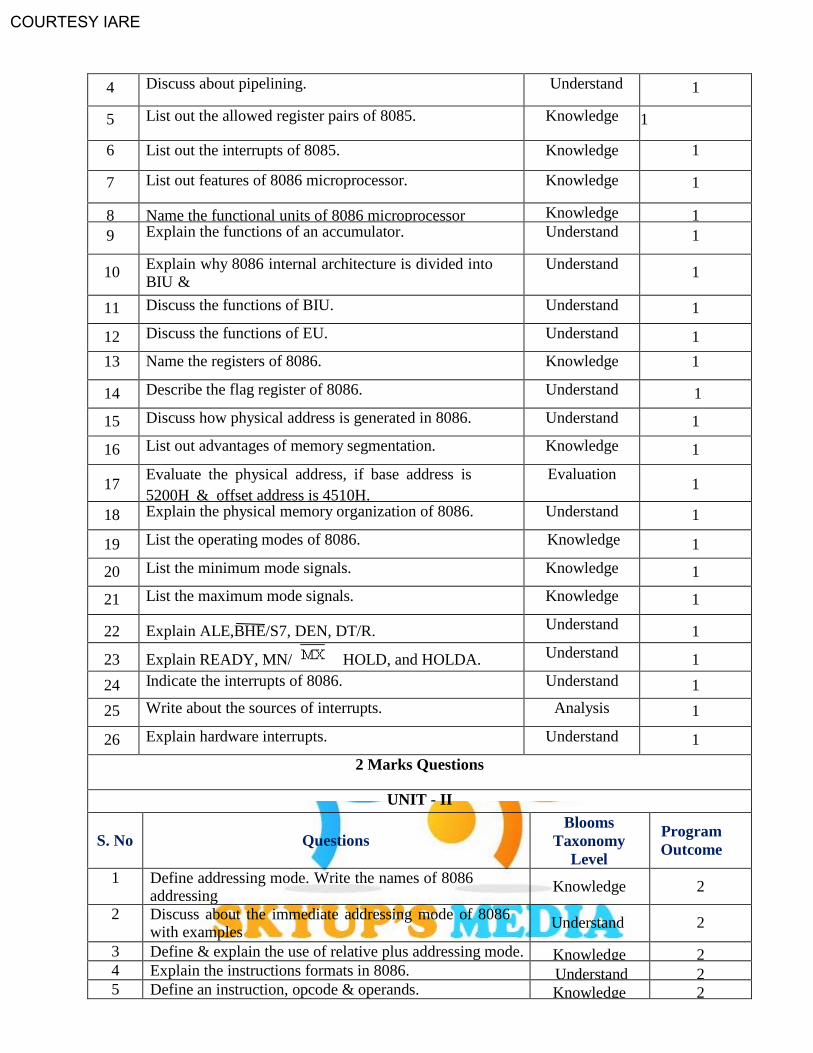
4 Discuss about pipelining. Understand 1
5 List out the allowed register pairs of 8085. Knowledge 1
6 List out the interrupts of 8085. Knowledge 1
7 List out features of 8086 microprocessor. Knowledge 1
8 Name the functional units of 8086 microprocessor Knowledge 1
9 Explain the functions of an accumulator. Understand 1
10 Explain why 8086 internal architecture is divided into BIU &
EU.
Understand 1
11 Discuss the functions of BIU. Understand 1
12 Discuss the functions of EU. Understand 1
13 Name the registers of 8086. Knowledge 1
14 Describe the flag register of 8086. Understand 1
15 Discuss how physical address is generated in 8086. Understand 1
16 List out advantages of memory segmentation. Knowledge 1
17 Evaluate the physical address, if base address is
5200H & offset address is 4510H.
Evaluation 1
18 Explain the physical memory organization of 8086. Understand 1
19 List the operating modes of 8086. Knowledge 1
20 List the minimum mode signals. Knowledge 1
21 List the maximum mode signals. Knowledge 1
22 Explain ALE,BHE/S7, DEN, DT/R. Understand 1
23 Explain READY, MN/ HOLD, and HOLDA. Understand 1
24 Indicate the interrupts of 8086. Understand 1
25 Write about the sources of interrupts. Analysis 1
26 Explain hardware interrupts. Understand 1
2 Marks Questions
UNIT - II
S. No
Questions Blooms
Taxonomy
Level
Program
Outcome
1 Define addressing mode. Write the names of 8086 addressing
modes.
Knowledge 2
2 Discuss about the immediate addressing mode of 8086 with examples
an example.
Understand 2
3 Define & explain the use of relative plus addressing mode. Knowledge 2 4 Explain the instructions formats in 8086. Understand 2 5 Define an instruction, opcode & operands. Knowledge 2
COURTESY IARE
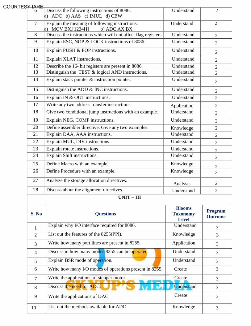
6 Discuss the following instructions of 8086. a) ADC b) AAS c) IMUL d) CBW
Understand 2
7 Explain the meaning of following instructions. a) MOV BX,[1234H] b) ADC AX,BX
Understand 2
8 Discuss the instructions which will not affect flag registers. Understand 2
9 Explain ESC, NOP & LOCK instructions of 8086. Understand 2
10 Explain PUSH & POP instructions. Understand 2
11 Explain XLAT instructions. Understand 2
12 Describe the 16- bit registers are present in 8086. Understand 2 13 Distinguish the TEST & logical AND instructions. Understand 2
14 Explain stack pointer & instruction pointer. Understand 2
15 Distinguish the ADD & INC instructions. Understand 2
16 Explain IN & OUT instructions. Understand 2
17 Write any two address transfer instructions. Application 2
18 Give two conditional jump instructions with an example. Understand 2
19 Explain NEG, COMP instructions. Understand 2
20 Define assembler directive. Give any two examples. Knowledge 2
21 Explain DAA, AAA instructions. Understand 2
22 Explain MUL, DIV instructions. Understand 2
23 Explain rotate instructions. Understand 2 24 Explain Shift instructions. Understand 2
25 Define Macro with an example. Knowledge 2
26 Define Procedure with an example. Knowledge 2
27 Analyze the storage allocation directives. Analysis 2
28 Discuss about the alignment directives. Understand 2
UNIT – III
S. No
Questions Blooms
Taxonomy
Level
Program
Outcome
1 Explain why I/O interface required for 8086. Understand
3
2 List out the features of the 8255(PPI). Knowledge 3
3 Write how many port lines are present in 8255. Application 3
4 Discuss in how many modes 8255 can be operated. Understand 3
5 Explain BSR mode of operation. Understand 3
6 Write how many I/O modes of operations present in 8255. Create 3
7 Write the applications of stepper motor. Create 3
8 Discuss the need for ADC. Understand 3
9 Write the applications of DAC Create 3
10 List out the methods available for ADC. Knowledge 3

COURTESY IARE
11 Explain key bouncing. Understand 3
12 Describe how to eliminate key bouncing. Understand 3
13 Write the control word format for BSR mode. Create 3
14 Write the control word format for I/O mode. Create 3
15 Write in which mode of I/O operation Bi-directional
data transfer takes place explain.
Create 3
16 Calculate the control port address of 8255 if the base address
is FFF0H.
Apply 3
17 Explain the function of handshaking signals. Understand 3
18 Distinguish be tween s t a t i c and d yn amic RAM
wi th examples.
Understand 4
19 Explain the purpose of BHE and A0 p ins on
the 8086microprocessor.
Understand 4
20 Define Memory mapped I/O. Knowledge 3
21 Define I/O mapped I/O. Knowledge 3
22 Explain the purpose of CE or CS pin on a memory chip. Understand 3
23 Write the input for chip select. Create 3
24 Explain, why the interrupt and trap flags cleared as part
of the interrupt response.
Understand 4
25 Explain the interrupt response. Understand 4
26 Define interrupt vector table. Knowledge 4
27 Define interrupt service routine. Knowledge 4
28 Distinguish t h e d i f f e r e n c e b e t w e e n M a s k a b l e
a n d Non- Maskable interrupts.
Understand 4
29 List out the interrupts of 8086. Knowledge 4
30 Write the priorities of 8086 interrupts. Create 4
31 Write how many interrupts can be handled by PIC. Create 4
32 List out the uses of int-03 interrupt. Knowledge 4
33 Explain with an example how overflow flag set. Understand 4
34 Explain what happens when trap flag is set. Understand 4
35 Explain why serial data transfer is preferred over
parallel data transfer.
Understand 5
36 Define synchronous data transfer. Knowledge 5
37 Describe the communication. Understand 6
38 Define modem. Knowledge 6
39 Define communication links. Knowledge 6
40 Define USART. Knowledge 6
41 Write the use of 8251 chip. Create 6
42 List out the features of 8251(USART). Knowledge 6
43 List out the serial communication standards available. Knowledge 6
44 Write the most commonly used signals in RS232. Create 6
45 Describe and sketch the frame format of mode word of 8251
Understand 6
COURTESY IARE
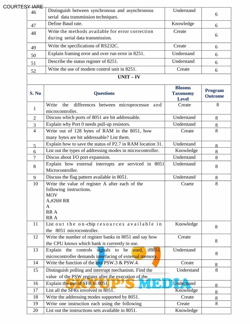
46 Distinguish between synchronous and asynchronous
serial data transmission techniques.
Understand 6
47 Define Baud rate. Knowledge 6
48 Write the methods available for error correction
during serial data transmission.
Create 6
49 Write the specifications of RS232C. Create 6
50 Explain framing error and over run error in 8251. Understand 6
51 Describe the status register of 8251. Understand 6
52 Write the use of modem control unit in 8251. Create 6
UNIT – IV
S. No
Questions Blooms
Taxonomy
Level
Program
Outcome
1 Write the differences between microprocessor and
microcontroller.
Create 8
2 Discuss which ports of 8051 are bit addressable. Understand 8
3 Explain why Port 0 needs pull-up resistors. Understand 8
4 Write out of 128 bytes of RAM in the 8051, how
many bytes are bit addressable? List them.
Create 8
5 Explain how to save the status of P2.7 in RAM location 31. Understand 8
6 List out the types of addressing modes in microcontroller. Knowledge 8
7 Discus about I/O port expansion. Understand 8
8 Explain how external interrupts are serviced in 8051
Microcontroller.
Understand 8
9 Discuss the flag pattern available in 8051. Understand 8
10 Write the value of register A after each of the
following instructions.
MOV
A,#26H RR
A
RR A
RR A
SWAP
A
Craete 8
11 List o u t t h e o n -chip r e s o u r c e s a v a i l a b l e i n
the 8051 microcontroller.
Knowledge 8
12 Write the number of register banks in 8051 and say how
the CPU knows which bank is currently in use.
Create 8
13 Explain the controls signals to be used, if8051
microcontroller demands interfacing of external memory.
Understand 8
14 Write the function of the bits PSW.3 & PSW.4. Create 8 15 Distinguish polling and interrupt mechanism. Find the
value of the PSW register after the execution of the
instructions.
MOV A, #95
ADD A, #120
Understand 8
16 Explain the use of SFR in 8051. Understand 8 17 List all the SFRs involved in 8051. Knowledge 8 18 Write the addressing modes supported by 8051. Create 8 19 Write one instruction each using the following
addressing modes.
a). Immediate b). Register c). Register indirect d). Direct
Create
Synthesis
8
8
a 20 List out the instructions sets available in 8051. Knowledge

COURTESY IARE
21 Explain the following instructions in 8051 micro controller. a. SETB 86H
b. CLR 87H
c. SETB 92H
Comprehension
8
22 Explain h o w 8051 differentiates internal and
external memory.
Understand 8
23 Differentiate t h e given 8051 instructions: MOVC
and MOVX.
Analyze 8
24 Explain the instructions LJMP and SJMP in 8051. Understand 8 25 Write the addressing mode used in t he
fo l lowing instructions:
MOV R1, #02H and MOV R1, 20H
Create 8
26 Write the result of the following code & where it is stored.
MOV R4,
#25H MOV
A, #1FH ADD
A, R4
Create 8
27 Write the content of register A after the execution of
the following code.
CLR A
ORA A,
#99H CPL
A
Create
8
28 Write the contents of AC, CY flags if we add 25H and 70H. Create 8
UNIT – V
S. No
Questions Blooms
Taxonomy
Level
Program
Outcome
1 Explain the format of TMOD & TCON. Understand 7 2 Describe the Timer counter logic diagram. Understand 7 3 Define serial communication in 8051. Knowledge 7 4 List out the advantages of serial data transfer. Knowledge 7
5 List the SFRs needed for serial communication in 8051. Knowledge 7
6 Explain the use of PCON register. Understand 7
7 Describe how serial port is used for data transfer. Understand 7 8 List out functions of SCON register of 8051. Knowledge 7 9 Write the different serial data transmission modes in 8051. Create 7
10 List the interrupts of 8051. Knowledge 7 11 Explain what should be loaded in TCON register to
start Timer0 & Timer1.
Understand 7
12 Explain how many interrupts are there in 8051. And
name them.
Understand 7
13 Write the highest priority interrupt of 8051. Create 7
14 Explain which port in 8051 microcontroller is bit
addressable .
Understand 7
15 Describe the SCON register in 8051. Understand 7
16 Write the format of IE register in 8051. Create 7 17 Explain under what conditions are the TI and RI bits raised. Understand 7

COURTESY IARE
18 Calculate baud rate in mode-1 operation. Apply 7
2. Group - II (Long Answer Questions)
UNIT – 1
S. No
Questions Blooms
Taxonomy
Level
Program
Outcome
1 Explain the architecture of 8086 with neat diagram. Understand 1 2 Compare 8085 & 8086 microprocessors. Analyze 1
3 Write the size of 8086 instruction queue and explain how
does queue speed up the processing.
Create 1
4 Explain general purpose & special purpose registers of
8086.
Understand 1
5 Explain the flag register of 8086. Understand 1 6 Discuss memory segmentation & mention its advantages. Understand 1
7 Describe the 8086 microprocessor pin-diagram. Understand 1 8 Discuss about the functions of the following pins.
a)TEST b) RQ/GT0 & RQ/GT1 c) QS0 & QS1 d) S0,S1,S2 Understand 1
1a 9 Explain minimum mode conf igura t ion of 8086
microprocessor.
Understand 1
10 Explain minimum mode control signals of 8086. Understand 1
11 Explain maximum mode configuration of 8086
microprocessor.
Understand 1
12 Explain maximum mode control signals of 8086. Understand 1
13 Explain the read & write timing diagrams for maximum
mode configuration.
Understand 1
14 Explain the read & write timing diagrams for minimum
mode configuration.
Understand 1
15 Describe the function of the following signals.
a) NMI b) c) d) RESET
Understand 1
16 Describe the interrupts of 8086. Understand 1
S. No
Questions Blooms
Taxonomy
Level
Program
Outcome
UNIT – II
1
Discuss the instructions formats of 8086. Understand 2
COURTESY IARE
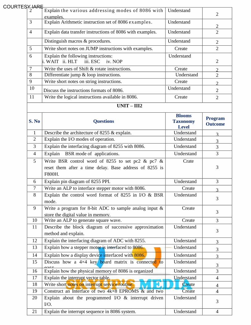
2 Explain the various addressing modes of 8086 with
examples.
Understand 2
3 Explain Arithmetic instruction set of 8086 examples . Understand 2
8086 with
4 Explain data transfer instructions of 8086 with examples. Understand 2
Distinguish macros & procedures. Understand 2
5 Write short notes on JUMP instructions with examples. Create 2
6 Explain the following instructions: i. WAIT ii. HLT iii. ESC iv. NOP
Understand
2
7 Write the uses of Shift & rotate instructions. Create 2 8 Differentiate jump & loop instructions. Understand 2
9 Write short notes on string instructions. Create 2 10
Discuss the instructions formats of 8086. Understand 2
11 Write the logical instructions available in 8086. Create 2
UNIT – III2
S. No
Questions Blooms
Taxonomy
Level
Program
Outcome
1 Describe the architecture of 8255 & explain. Understand 3 2 Explain the I/O modes of operation. Understand 3 3 Explain the interfacing diagram of 8255 with 8086. Understand 3
4 Explain BSR mode of applications. Understand 3
5 Write BSR control word of 8255 to set pc2 & pc7 &
reset them after a time delay. Base address of 8255 is
F800H.
Crate 3
6 Explain pin diagram of 8255 PPI. Understand 3
7 Write an ALP to interface stepper motor with 8086. Create 3 8 Explain the control word format of 8255 in I/O & BSR
mode.
Understand 3
9 Write a program for 8-bit ADC to sample analog input &
store the digital value in memory.
Create 3
10 Write an ALP to generate square wave. Create 3
11 Describe the block diagram of successive approximation
method and explain.
Understand 3
12 Explain the interfacing diagram of ADC with 8255. Understand 3 13 Explain how a stepper motor is interfaced to 8086. Understand 3
14 Explain how a display device interfaced with 8086. Understand 3 15 Discuss how a 4×4 key board matrix is connected to
8255.
Understand 3
16 Explain how the physical memory of 8086 is organized Understand 3
17 Explain the interrupt vector table. Understand 4
18 Write short notes on interrupt service routine. Create 4 19 Construct an Interface of two 4k×8 EPROMS & and two
4k×8 RAM chips with 8086. Select suitable memory map.
Create 4 e 20 Explain about the programmed I/O & interrupt driven
I/O.
Understand 3
21 Explain the interrupt sequence in 8086 system. Understand 4
COURTESY IARE
22 Write short notes on 5 types of interrupts supported by
8086.
Create 4
23 Describe the 8251 with neat block diagram. Understand 5 24 Discuss how 8251 is used for serial communication of
data.
Understand 5
25 Explain the advantages of using the USART chips in
microprocessor based systems.
Understand 5
26 Discuss the types of serial communication. Understand 6 27 Explain the interfacing of 8251 with 8086 with
necessary circuit diagram
Understand 6
28 Discuss the data transmission standards and their
specifications
Understand 6
29 Write t h e M O D E M c o n t r o l lines and e xplain
the functioning of each line.
Create 6
30 Explain the pin structure of RS232C & also discuss
about voltage & current specifications of RS 232C.
Understand 6
31 Describe the logic diagram to convert TTL to RS232C
conversion and RS232C to TTL conversion.
Understand 6
UNIT – IV
S. No
Questions Blooms
Taxonomy
Level
Program
Outcome
1 Discuss the register set of 8051 and also discuss how
memory and I/O addressing is done in 8051.
Understand 8
2 Discuss internal architecture of 8051 microcontroller in
detail.
Understand 8
3 Describe the five addressing modes of 8051
microcontroller with example.
Understand 8
4 Sketch and illustrate how to access external memory
devices in an 8051 based system.
Apply 8
5 Discuss the internal memory organization of the 8051
microcontroller.
Understand 8
6 Design an 8051 based system with 16 K bytes of
program ROM and 16 K bytes of data ROM.
Create 8
7 Discuss ab o u t the memory organization and special
function registers in 8051 microcontroller.
Understand 8
9 Describe the operation of I/O ports in 8051 with neat
sketch.
Understand 8
10 Demonstrate the functioning of A & B registers of 8051.
Apply 8
11 List the format of PSW register of 8051 and explain
each bit.
Knowledge 8
UNIT – V
S. No
Questions Blooms
Taxonomy
Level
Program
Outcome
1 Discuss in detail the various modes of operation of timers
in 8051.
Understand 8
2 Express about external hardware interrupt in 8051. Understand 8
3 Discuss about serial communication in 8051
microcontroller.
Understand 8
COURTESY IARE
4 Label the format of IE & IP formats & explain. Knowledge 7
5 Explain the function and operating modes with the
associated registers of Timer/Counter in 8051
microcontroller.
Understand 7
6 Write the sequence of events that takes place when the
interrupt occurs in 8051.
Create 7
7 Examine the various SFRs you need while handling the
timers/counters. Give the register formats.
Analyze 7
8 Explain the various modes of serial port in 8051. Understand 7
9 Discuss the format & bit definitions of SCON register. Understand 7
10 Describe the TCON and TMOD registers of 8051. Understand 7

COURTESY IARE
3. Group - III (Problem solving &Analytical Questions):
UNIT – I
S. No
Questions Blooms
Taxonomy
Level
Program
Outcome
1 Calculate the effective address & physical address of the
following instructions.
(a) IMUL AX, [BP + BX – 8D] (b) SBB AL, ES:[ SI +
5D] (c) PUSH AX (d) AND AH, [SI + 42D] (e) CMPSB
(f) CMPB DX, [SI]
Assume CS = 5000H, DS = 8000H, SS = A000H, ES =
B000H, SI = 2000H, DI = 6000H, BP = 1002H, SP =
0002H, AX = 0000H, BX = 5200H, CX = 2000H.
Apply
1
2 Calculate the physical address is represented by
i) 4370:561EH ii) 7A32:0028H
Apply
1
3 Evaluate the physical address of the top of the stack? If
the stack segment register contains 3000h and the stack
pointer register contains 8434H.
Evaluate
1
4 Identify the memory address of the next instruction
executed by the microprocessor, when operated in the real
mode, for the following CS:IP combinations:
a) CS = 1000H and IP = 2000H
b) CS= 2000h and IP=10000h
Understand
1
UNIT – II
S. No
Questions Blooms
Taxonomy
Level
Program
Outcome
1 Write a program to read ASCII code after a strobe signal
is sent from a Keyboard.
Create 2
2 Develop a program to add a profit factor to each element
in a cost array and puts the result in a prices array.
Create 2
3 Write an ALP for add a 5-byte number in one array to a 5
byte in another array. Put the sum in another array. Put the
state of the carry flag in byte 6 of the array that contains
the sum. The first value in each array is the least
significant byte of that number.
Create 2
4 Write a delay loop which produces a delay of 500µsec on
an 8086 with 5-MHz clock.
Create 2
5 Write an assembly language program to find factorial of a
given number.
Create 2
6 Write an assembly language program to find sum of
squares.
Create 2

COURTESY IARE
7 Write an assembly language program to find number of
positive & negative numbers from a given array.
Create 2
8 Write an assembly language program to convert ASCII to
BCD.
Create 2
9 Write an ALP to find cube of an 8-bit hexadecimal
number.
Create 2
10 Write an ALP to display ‘IARE MPMC LAB’ on the
screen.
Create 2
11 Write an ALP to convert a given sixteen bit binary
number to its gray equivalent.
Create 2
UNIT – III
S. No
Questions
Blooms
Taxonomy
Level
Program
Outcome
1 Model a Control Words When the Port Of Intel 8255A
defined as follows: Port A as an O/P port, mode of the
port a is mode-0, port B as an O/P port, mode of the Port B
is mode-0.
Analyze 3
2 Construct an Interfacing DAC AD7523 with an 8086 CPU
running at 8MHZ and write an assembly language
program to generate a sawtooth waveform of period 1ms
with Vmax 5V.
Apply
3
3 Write an ALP for stepper motor interfacing by using loop
instructions.
Create 3
4 Construct an interface two chips of 32k × 8 PROM & four
chips of 32k × 8 RAM with 8086, according to the
Following map.
ROM 1 & 2 F0000H-FFFFFH, RAM 1 & 2 D0000H-
DFFFFH RAM 3 & 4 E0000H-EFFFFH. Show t h e
implementation of this memory system.
Apply
4
5 Illustrate the status register of 8251 for the given
statement.
Read status register and wait for DSR and TxRDY to
become active. One active, get character from PC
keyboard using INT B8H (keyboard routine).
Apply
Analysis
4
6 Write an ALP for to transfer the data serially. Create 6
7 Identify the errors in receiving the data from
asynchronous mode of operation using 8251.
Knowledge 6
8 Write the sequence of instructions required to initialize
8251 at address A0H and A1H for the configuration
below.
i) Character length – 8 bits
ii) No parity
iii) Stop bits – 2
iv) Baud rate – 16 X
v) Error flag is reset
vi) DTR and RTS asserted
Create
6
b
UNIT – IV
S. No
Questions Blooms
Taxonomy
Level
Program
Outcome
1 Write 8051 program to convert packed BCD number
available in accumulator, into two ASCII numbers and
save them in internal RAM locations 48H and 49H.
Create
8
2 Develop 8051 program to move a block of data from
external program memory to external data memory.
Create 8

COURTESY IARE
3 Use PUSH instruction to put the number 82H in RAM
locations 34H to 37H. also write same program without
PUSH instruction.
Analyze
8
4 Generate a program in 8051 to count number of zero bits
available in a byte available in external RAM at 1000h.
Store zero bit count in internal RAM location 60H.
Create 8
5 Write 8051 program to OR the contents of port 1 and port 2,
put the result in external RAM location 0102h.
Create 8
UNIT – V
S. No
Questions Blooms
Taxonomy
Level
Program
Outcome
1 Indicate when the TF0 flag is raised for the following
program.
MOV TMOD, #01H
MOV TL0, #12H MOV
TH0, #1CH SETB TR0
Assume XTAL = 11.0592MHz.
Understand
ion
7
2 Examine the TH1, TL1 value to generate a time delay of
5ms. Timer 1 is programmable in mode 1. Assume that
XTAL = 16MHz
Analyze
7
3 Write a Program for Timer 1 to generate a square wave of
1 kHz. Assume that XTAL = 11.0592MHz.
Create 7

COURTESY IARE