electronics and communication engg. title: pcb design and
TRANSCRIPT
PCB DESIGN AND FABRICATION LAB 2020-2021
Course Coordinator: Mallikarjun S H. Lecturer ECE programme, GPT Kampli. Page 1
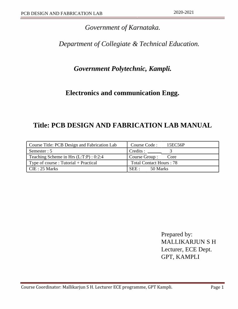
Government of Karnataka.
Department of Collegiate & Technical Education.
Government Polytechnic, Kampli.
Electronics and communication Engg.
Title: PCB DESIGN AND FABRICATION LAB MANUAL
Course Title: PCB Design and Fabrication Lab Course Code : 15EC56P
Semester : 5 Credits : 3
Teaching Scheme in Hrs (L:T:P) : 0:2:4 Course Group : Core
Type of course : Tutorial + Practical Total Contact Hours : 78
CIE : 25 Marks SEE : 50 Marks
Prepared by:
MALLIKARJUN S H
Lecturer, ECE Dept.
GPT, KAMPLI

PCB DESIGN AND FABRICATION LAB 2020-2021
Course Coordinator: Mallikarjun S H. Lecturer ECE programme, GPT Kampli. Page 2
PCB DESIGN AND FABRICATION LAB
1.1 Introduction:
PCB, short for printed circuit board, is the supplier of electronic components and electronic
interconnections. The key advantage of PCBs lies in its capability to greatly reduce the errors of routing and
assembly and to increase the degree of automation and fabrication efficiency. Due to decades' development,
PCBs have been constantly contributing to the improvement and progress of people's modern life .
PCBs can be classified into different categories according to different classification standards. Based on the
number of layers, PCBs can be classified into single-layer PCBs (also called single-sided PCBs), double- layer
PCBs (also called double-sided PCBs) and multi-layer PCBs. Based on the substrate material, PCBs can be
classified into rigid PCBs, flexible PCBs and flex-rigid PCBs. Based on application fields, PCBs can be
divided into low-frequency PCBs and high-frequency PCBs. With the development of technology and the
advent of new substrate, some special types of PCBs come into being, such as metal core PCBs, SMT PCBs,
high-Tg PCBs, carbon-film PCBs, etc. Each type of PCBs is applied in different fields owing to their
advantages together with consideration of their disadvantages
Single-layer PCBs
As the most fundamental type of PCBs, single-layer PCBs contain only one layer of substrate or
base material whose one side is covered with a thin layer of metal, copper for most times due to its excellent
conductivity. Outside copper is a layer of solder mask that plays a protective role in PCB and silk screen coat
is outermost. The structure of a single-layer PCB is best shown in the image below.
Advantages of single-sided PCBs include:
• Low cost, especially for volume production;
• Low rate of issues during PCB manufacturing process, accordingly, leading to high speed of fabrication;
• Suitable for simple circuits.
For engineers or hobbyists who need single-layer PCBs for simple projects, you can try to make PCBs at home
or in your own laboratory with fundamental tools. However, you should rely on reliable PCB
manufacturers when working on advanced projects or products requiring high quality and excellent
performance.

PCB DESIGN AND FABRICATION LAB 2020-2021
Course Coordinator: Mallikarjun S H. Lecturer ECE programme, GPT Kampli. Page 3
Single-layer PCBs have a relatively wide field of applications ranging from power supplies, relays, sensors
and LEDs to calculators, printers, coffee makers and electronic toys. However, single-sided PCBs feature
some performance limitations deriving from EMC, EMI, density etc. In terms of complex circuits, it's
double-layer PCBs or multi-layer PCBs that should be depended on.
Double-layer PCBs
Double-layer PCBs, also called double-sided PCBs, can be regarded as the most widely-used type of PCB,
allowing for the routing of traces around each other by jumping between a top and bottom layer through vias.
Different from single-sided PCBs that have only one conductive layer, double-layer PCBs have two
conductive layers that are placed on both sides of substrate and so are components.
Vias or holes connect both sides of boards through two methods: through-hole technology and surface
mount technology (SMT). Up to now, SMT is more popular as it allows more circuits to be attached
to board with space saved, weight reduced and manufacturing speed increased.
Therefore, advantages of double-layer PCBs can be summarized into the following aspects:
• More flexibility for designers;
• An increase of circuit density;
• Relatively low cost;
• Reduction of board size.
Owing to its benefits, double-sided PCBs have covered a wide range of applications including power
supplies, industrial control, control relays, converters, UPS system, LED lighting, hard drives, printers,
mobile phone system, power monitoring, test equipment, amplifiers, traffic systems etc.
Multi-layer PCBs
Multi-layer PCBs further increase the complexity and density of PCB designs by adding additional layers
beyond the top and bottom layers seen in a double-sided configuration. They can be regarded as expansion of
double-layer PCBs. With the availability of over thirty layers in multilayer PCBs configurations, multi- layer
PCBs allow designers to produce very dense and highly complex designs. Quite often the extra layers in these
designs are used as power planes, which supply the circuit with power also reduce the electromagnetic
interference levels emitted by designs. Lower EMI levels are achieved by placing signal levels in between
power planes. It's also of note that increasing the number of power planes in a PCB design

PCB DESIGN AND FABRICATION LAB 2020-2021
Course Coordinator: Mallikarjun S H. Lecturer ECE programme, GPT Kampli. Page 4
with increase the level of thermal dissipation a PCB can provide, which is important in high power designs.
Similar to double-layer PCBs, components on multi-layer PCBs are interconnected with each other through
holes or vias as well.
Advantages of multi-layer PCBs include:
• Reduction of board size and weight; • Higher level of density and flexibility;
• Capable of implementing multiple functions;
• Better at dealing with interference.
1.2 TERMINOLOGIES IN PCB DESIGNS ---
Many of us design PCB with the information available on internet but sometimes it becomes difficult
to understand the terms used in PCB designing. In this article I have tried to explain the common terms
which are used while designing PCBs. PCB stands for printed circuit board. Different types of PCB
materials are available in markets. Most commonly used are FR-1, FR-2, CEM-3, CEM-1 (FR=Flame
Retardant and CEM= Composite Epoxy Material).
Common terms used are as follows-
1. Layers Everything which you draw is on layer. Each layer has different physical properties. For example top layer is used to draw the component layout, bottom layer or inner layer are used for making connection between components and many more are also present.
2. Footprint Footprint is the collection of pads and outline which make an individual component. PCB design software comes with a library which contains footprints of different components but the number of footprints that are available is limited. As we know today technology is changing and size of components is reducing, so sometimes we have to make the footprint of the component.
3. Solder mask
You all have seen the green, red, blue or shiny coating on the PCB. This coating is known as solder mask. Masking is done to avoid the solder which accidently drops on PCB and soldering of component also become easy. This also prevents the short circuit among close track. Being a beginner it may possible we

PCB DESIGN AND FABRICATION LAB 2020-2021
Course Coordinator: Mallikarjun S H. Lecturer ECE programme, GPT Kampli. Page 5
use excess of solder while soldering which may short the tracks, if solder mask is there it can be
easily removed without melting.
This is on copper side). This can also be used to indicate the name of the company or manufacturer. This is a
non conducting layer of a PCB.
5. Jumper Jumper wire forms electrical connections between two points on printed circuit board. Sometimes it happen while designing PCB that tracks may overlap each other as we make connections; in that case we used jumper wire.
6. Pads
Pads are used to make connections between component and track with the help of solder.Pads are
small surface of copper available on printed circuit board. They are basically used to solder the leads
of the components on board to make the mechanical joint strong. Different kinds of pads are used
for Surface mount component and through hole component as shape and size of both the components vary
from one another. a non conducting layer of a PCB.
4. Silkscreen
Silkscreen is done to represent the name or value of components so that user can easily identify the
component during soldering. This is a good practise while designing the PCB. Silk-screening can be done on
both sides of PCB (on component side or
7. Copper traces
You have seen that green, blue or red lines are used to connect pads and vias. They are known as copper traces.
They provide electrical conduction between pads and vias or between two pads and vias. Width of track varies
according to the current flow through them.
8. Via Suppose you are designing multilayer PCB and you want the connection between bottom layer and top layer then we use via. Via allows the current to pass through the board. This can be seen in the figure below. In

PCB DESIGN AND FABRICATION LAB 2020-2021
Course Coordinator Mallikarjun S H. Lecturer ECE programme, GPT Kampli. Page 6
this consider yellow colour pads as bottom layer and green colour pads as top layer so the yellow color
circle shown are via.
Basically following colours are used to indicate the layers in multilayer PCB-
The PCB in figure shows a track that belongs to the top layer that goes through the board using a thru-hole
via, and then continues a track that belongs to the bottom layer.

PCB DESIGN AND FABRICATION LAB 2020-2021
Course Coordinator: Mallikarjun S H. Lecturer ECE programme, GPT Kampli. Page 7
9. Blind via
In more complex circuit generally in designing integrated circuits where more power planes (Gnd and Vcc) are used we prefer via. We used vias between top layer and second layer not in the bottom layer. These vias are called blind vias. Because it i easy to directly connect the power planes that are beneath the chips instead of routing long tracks. Blind vias are used when connection has to be made from external layer to internal layer with minimum vias height. You can identify that the vias used are through hole or blind. Just put your PCB on source of light and see if light is coming from source through via. If you can see the light , then the via is through hole otherwise it a blind via. This technique is useful where you don't have much space for placing the component and routing. If you use through hole via instead of blind then it would need some extra space by vias on both sides. From the figure below you can see that one blind via is connect between top layer and inner layer(red colour
and yellow colour) and another blind vai is connected between inner layer and bottom layer( blue and light
blue). And in the similar figure where all three colour are present is a through hole via connecting top and
bottom layer.
10.BuriedVias
Buried vias are similar to blind vias but they only make connection between the inner layers. From the figure you can see that yellow and light blue colours represent the buried vias. From figure below you can compare all three vias as follows-
· First one that is red yellow light blue and blue represent through hole via. · Second one that is red and yellow represent blind via.
· Third one that is yellow and light blue represent buried via.

PCB DESIGN AND FABRICATION LAB 2020-2021
Course Coordinator: Mallikarjun S H. Lecturer ECE programme, GPT Kampli. Page 8
Main disadvantage of using buried via is it will increase the cost of PCB as compared to through hole via. But
advantage of using buried vias is smaller size. So depending upon the requirement one can use the type suitable
to it.
11. Gerber Gerber file is send by user to manufacture to make PCB. Gerber file is important because many PCB design software are available now a days and it is not necessary that software which you are using will be available at vendor side. Suppose I make my PCB on Eagle software and my PCB manufacturer does not have the
same, at that time gerber file is useful. So now Gerber file will help manufacture to know your project and
manufacturer cannot make changes in Gerber file. Gerber file contain information about drill size, where to
make hole, how tracks are connected, naming of components etc.
12. BOM
BOM represent bill of material. It gives you the list of component present on PCB. So that you can calculate
the approximate cost and it becomes easy for you to order the components. With this you can cross check the
components you forgot by mistake.
1.3 STEPS INVOLVED PCB DESIGN AND FABRICATION PROCESS
1. Schematic and Simulation.
2. PCB Layout design.
3. Fabrication.
1.3.1Soft ware’s used:
1. Multisim —
2. Dip Trace ----
For Schematic and simulation.
For Layout Design
Other soft ware’s available: Circuit maker, ExpressPCB, Electronic workbench, ORCAD, KiCAD,
Eagle etc.
1. Schematic and Simulation Procedure :( MultiSim Software)
1. Open the Multisim 8.0 Software i.e. Go to ----Start--All Programs--Electronic workbench---Multisim---multisim8.0.Click it
2. After launching, it opens Spread sheet, Design toolbox in the main page.
3. Go to Component tool bar (Symbols Shown) , Click and drag all the components and
place them in a spread sheet and make the wire connection as per schematic circuit.

PCB DESIGN AND FABRICATION LAB 2020-2021
Course Coordinator: Mallikarjun S H. Lecturer ECE programme, GPT Kampli. Page 9
4. Connect the Measuring instruments (multimeter, CRO, Function generator etc.) at the
output side of the schematic which are located at right side of the main window.
5. Run the Simulation. I.e. Go to Simulate---Run and click it.
6. Observe the result and analyze the schematic for different values of input parameters.
2. PCB Layout Design Procedure :(DipTrace Software)
A) Steps Involved in Manual Routing. 1. Open the DipTrace software i.e. Go to Start ->DipTrace ->PCB Layout Editor,
Click on it.
2. After Launching, it opens the Spread sheet in the main window.
3. Prior to draw a layout do the following settings. Sclale-200%, Grid size-2.54mm
and Change the Component tool bar settings as Bottom Side, Bottom Assy,
Bottom(2) in the main window since by default shown as TOP side.
4. Go to Place Component and drag all the components (packages) required as per
the schematic circuit into spread sheet. 5. Place the components properly and go to Route Manual click on it and Start to
connect the tracks (copper trace) b/w the components without any overlap. 6. After Completion of track design, Select the whole diagram and right click on it, go
to net properties Change Trace width as 1.5mm. 7. Again Select the Whole diagram and right click on pad and then go to pad
properties change Pad width =3mm and pad height=3mm and diameter=0.5mm .
8. Go to Verification Do Check design rules (ERC) for error detection.
9. Save the File in any Folder.
10. Measure the Size of the board by using “Measure” icon on the tool bar. Maintain the
size of PCB Layout design to fit into a Board of standard size as 3x4 inches.
3. PCB Fabrication process Steps:
1.Take a single sided PCB and scrub the copper clad for a while to remove unwanted particles on it.
2.Take a printed layout photo paper and attach it on copper clad properly using cello tape.
3.Take metallic iron box and let it charged for around 100degree and transfer the heat
on photo paper which is attached to the PCB board.
4.After transferring heat at about 2 to 3 min , the image(trace) is completely transferred it on
copper clad of the board and then dip into water to remove photo paper.
5.Etching: Once it is cleaned then next process is to remove unwanted copper and this called
as etching process. In this process we use ferric chloride+ water(1:3ratio) solution
to remove unwanted copper.
6.Once the solution (fecl3+water) is prepared in the tray , then dip the board in the solution and
keep it for 1 hour.(shake the tray to remove copper at faster rate)
7. Take out the board from the tray and check ,Once copper is get removed except in the
layout area of the board. Pour ACETONE on the board then clean it using waste cloth
,which removes ink or toner on the copper trace.
8.After removing ink or toner then Clean the copper trace on the board using scrubber to
remove unwanted chemicals. 9. Test the connectivity of the tracks by using multimeter if any short is present in the
design.

PCB DESIGN AND FABRICATION LAB 2020-2021
Course Coordinator: Mallikarjun S H. Lecturer ECE programme, GPT Kampli. Page 10
10. Once tested ok .Place and mount the components on the board according to the schematic
and solder it properly.
11. Check and analyze the result by Power up the circuit.
1.4 PCB LAYOUT DESIGN COMPONENT PACKAGE LIST
SL.NO. Component name Package name
1 Resistor RES-10.16/5.1x2.5
2 Capacitor(Electrolyte) CAPPR-5.08/7.62
3 Capacitor(Ceramic) CAPP-5.08/9.15x3
4 Diode D-07
5 LED LED-100
6 Transistor TO-9
7 Potentiometer POT-15 DIP-8, DIP-16, DIP-
8 IC'S 14…
9 7805 Regulator TO-220
10 Switch B3F-3/X6.15
11 Crystal HU-49U
12 DB-9 Connector DB9F
1.5 NET PROPERTIES AND PAD PROPERTIES SETTINGS
Width Height Diameter/Shape
Trace width 1.5mm ----- -------
Pad Size 3mm 3mm 0.5mm(Round)
For IC'S 2mm 2mm Rectangle
FOR Transistors 2mm 2mm Rectangle
Note: For SUPPLY, GROUND and TRANSFORMER Create Pads in the PCB and make the connection

PCB DESIGN AND FABRICATION LAB 2020-2021
Course Coordinator Mallikarjun S H. Lecturer ECE programme, GPT Kampli. Page 11
LIST OF MATERIALS FOR PARTICIPANTS FOR PCB
FABRICATION AND DESIGNING LAB : 1. PCB COPPER CLAD 6*4 ----25 NOS 2. FECL3 UNHYDROUS CHEMICAL ---500GMS *2
3. PLASTIC TRAY -----03 NOS
4. PCB MANUAL DRILLING MACHINES ----05
5. PHOTO PRINT PAPERS ----50 N0S A4 SIZE
6. NC THINNER ---- 500ML *2 NOS
7. DRILL BIT 1MM--- 20NOS
8. SMALL HACKSAW FRAME AND BLDE---02NOS
9. CELLO TAPE ROLL ---02NOS
10. LASER PRINTER
11. ELCTRIC AUTOMATIC IRON
12. PC WITH EDA SOFTWARES
13. MARKER PEN 0.5MM ---02NOS
14. WASTE CLOTHES.
FOR SAMPLE CIRCUIT PREPARTAION ---
15. MISC COMPONENTS AS PER THE CIRCUIT
16. LEAD
17. FLUX
18. SOLDERING IRONS
19. POWER SUPPLIES

PCB DESIGN AND FABRICATION LAB 2020-2021
Course Coordinator: Mallikarjun S H. Lecturer ECE programme, GPT Kampli. Page 12
EXP.1 7805 REGULATED POWER SUPPLY Aim--- to design the schematic and pcb layout of 7805 regulator circuit and prepare the pcb design Tools and equipments dip trace eda tool. Material required: Copper clad, photo print paper,fecl3 chemical, drill machine, drill bit 1mm ,laser printer.
CIRCUIT DIAGRAM
XMM2
2 V1 T1
230 V
U2
LM7805KC 8
D1 LINE VREG 1 9 VOLTAGE
COMMON
1N4007
R1
120
50 Hz 5 0Deg
TS_POWER_10_TO_1
D2 C1 C2 7 0
4
1N4007
1000uF-POL 100nF LED1
(B)Layout diagram

PCB DESIGN AND FABRICATION LAB 2020-2021
Course Coordinator: Mallikarjun S H. Lecturer ECE programme, GPT Kampli. Page 13
2
11
%
1
8
N
D
U1
EXP.2 ASTABLE MUTIVIBRATOR USING 555 IC Aim--- to design the schematic and pcb layout of astable multivibrator using 555 timer ic circuit and prepare the pcb design tools and equipments dip trace eda tool. Material required: Copper clad, photo print paper, fecl3 chemical, drill machine, drill bit 1mm ,laser
printer.
CIRCUIT DIAGRAM: +5
D2 R1 LE 10k
4 3 R Q
7 DC
5 CV
RV2
R2
Q1
220R BC548
C1 TR
10n TH 6
100K
C2 555
10u
VCC 5V
VCC R4 6
100K _LIN Key = A
R3
85%
R1 120
10k LED1 3
8 U1
VCC 7
4 RST OUT 3 7 4
DIS R2 Q1
8 6 THR 5
C1 2 TRI
1 5
220
CON BC548A
10uF-POL GND
1 LM555CN
C2
0
10nF
(b)Layout Diagrm

PCB DESIGN AND FABRICATION LAB 2020-2021
Course Coordinator: Mallikarjun S H. Lecturer ECE programme, GPT Kampli. Page 14
EXP.3 FULL ADDER USING HALF ADDERS Aim--- to design the schematic and pcb layout of full adder using half adders r circuit and prepare the pcb design Tools and equipments dip trace eda tool. Material required: Copper clad, photo print paper, fecl3 chemical, drill machine, drill bit 1mm ,laser
printer.
CIRCUIT DIAGRAM
VCC 5V J1 2 U1
AND2
X1
3
U5 2.5 V 10
Key = A U3
VCC J2 1
OR2 4
U2
Key = B
EOR2 6
X2 AND2
U4 2.5 V5
9
J3
EOR2
0
Key = C
Schematic Diagram

PCB DESIGN AND FABRICATION LAB 2020-2021
Course Coordinator: Mallikarjun S H. Lecturer ECE programme, GPT Kampli. Page 15
(b) Lay out Diagram
TRUTH TABLE
A B C SUM CARRY
0 0 0 0 0
0 0 1 1 0
0 1 0 1 0
0 1 1 0 1
1 0 0 1 0
1 0 1 0 1
1 1 0 0 1
1 1 1 1 1
Expressions: Sum=A xor B xor C.
Carry=(A xor B)C+ AB

PCB DESIGN AND FABRICATION LAB 2020-2021
Course Coordinator: Mallikarjun S H. Lecturer ECE programme, GPT Kampli. Page 16
EXP.4. RC PHASE SHIFT OSCILLATOR CIRCUIT
Aim--- to design the schematic and pcb layout of RC phase shift oscillator circuit and prepare the pcb
designTools and equipments dip trace eda tool.
Material required: Copper clad, photo print paper, fecl3 chemical, drill machine, drill bit 1mm ,laser
printer.
CIRCUIT DIAGRAM:
R=4.7KOhm, C=100Nf, R1=47kohm,RL=2.2Kohm,Re=680Ohm,Ce=10uF,Cc=1uF
(b) Layout diagram

PCB DESIGN AND FABRICATION LAB 2020-2021
Course Coordinator: Mallikarjun S H. Lecturer ECE programme, GPT Kampli. Page 17
R1
0 1
R4
EXP.5 SUMMING AMPLIFIER USING OPAMP.
Aim--- to design the schematic and pcb layout of summing amplifier circuit and prepare the pcb design
Tools and equipments dip trace eda tool.
Material required: Copper clad, photo print paper, fecl3 chemical, drill machine, drill bit 1mm ,laser
printer.
CIRCUIT DIAGRAM:
R=1KOhm, IC741 R3 1.0k
VCC
12V
V2 3 0 2 VCC
XMM1
5 V 1.0k 7 1 5 U2
V1 R2 0 3
6 0
1 V 1.0k
6 2
V3 0 5
4 741
3 V 1.0k
VEE
-12V
(b) Layout diagram
VEE

PCB DESIGN AND FABRICATION LAB 2020-2021
Course Coordinator: Mallikarjun S H. Lecturer ECE programme, GPT Kampli. Page 18
EXP.6 THE FULL WAVE BRIDGE RECTIFIER WITH FILTER.
Aim--- to design the schematic and pcb layout of summing amplifier circuit and prepare the pcb design
Tools and equipments dip trace eda tool.
Material required: Copper clad, photo print paper, fecl3 chemical, drill machine, drill bit 1mm ,laser
printer.
CIRCUIT DIAGRAM:
D=1N4007, R=1KOhm,C=10uf
XSC1 G
T
3
1 V2
T1
A B
2 D1
230 V 4 1 5
50 Hz 0Deg
2 TS_POWER_10_TO_1 3 1B4B42
C2
10uF-POL
R1 1.0k
4 0
(b) Layout design

PCB DESIGN AND FABRICATION LAB 2020-2021
Course Coordinator: Mallikarjun S H. Lecturer ECE programme, GPT Kampli. Page 19
EXP 8. 4-BIT BINARY COUNTER
Aim--- to design the schematic and pcb layout of 4-bit binary counter circuit and prepare the pcb designTools and equipments dip trace eda tool.
Material required: Copper clad, photo print paper, fecl3 chemical, drill machine, drill bit 1mm ,laser printer’
VCC
5V
U1 U6 3
AND2 AND2
U2 U3 U4 6 U5
SET SET SET SETVCC 2 5
J Q J Q 1
4 J Q J Q
CLK CLK CLK CLK
XFG1
K ~Q K ~Q K ~Q K ~Q
RESET RESET RESET RESET 7
JK_FF JK_FF JK_FF JK_FF
0 X3 X4
X1 X2
2.5 V
2.5 V
2.5 V 2.5 V
Truth table Hex.No. X4 X3 X2 X1
1 0 0 0 1
2 0 0 1 0 3 0 0 1 1
4 0 1 0 0
5 0 1 0 1
6 0 1 1 0
7 0 1 1 1 8 1 0 0 0
9 1 0 0 1
10(A) 1 0 1 0 11(B) 1 0 1 1
12 (C) 1 1 0 0
13(D) 1 1 0 1
14(E) 1 1 1 0
15(F) 1 1 1 1

PCB DESIGN AND FABRICATION LAB 2020-2021
Course Coordinator: Mallikarjun S H. Lecturer ECE programme, GPT Kampli. Page 20
(b)Layout Diagram
PCB DESIGN AND FABRICATION LAB 2020-2021
Course Coordinator Mallikarjun S H. Lecturer ECE programme, GPT Kampli. Page 21
4
4
%
4
8
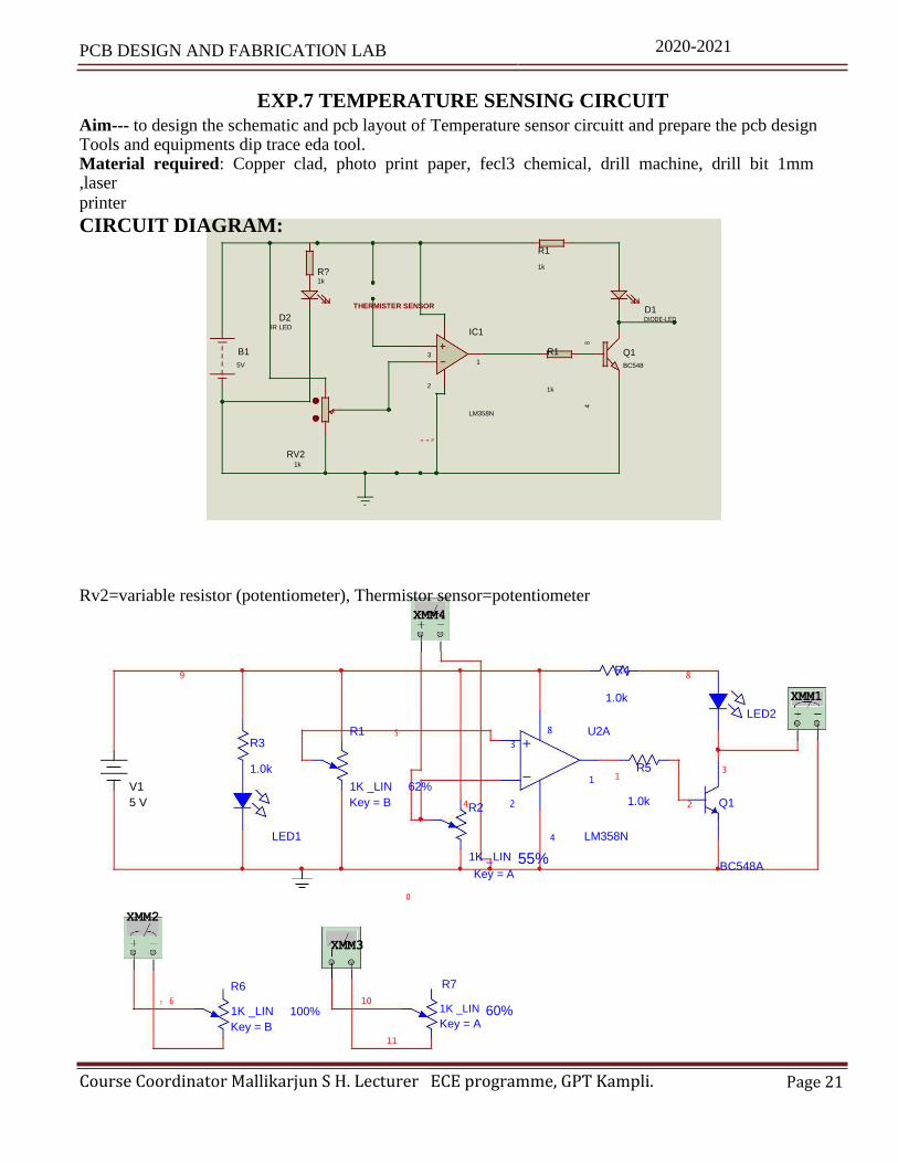
EXP.7 TEMPERATURE SENSING CIRCUIT
Aim--- to design the schematic and pcb layout of Temperature sensor circuitt and prepare the pcb design Tools and equipments dip trace eda tool. Material required: Copper clad, photo print paper, fecl3 chemical, drill machine, drill bit 1mm ,laser
printer
CIRCUIT DIAGRAM:
R1
1k R? 1k
THERMISTER SENSOR D1
D2 DIODE-LED
IR LEDIC1
B1 3 R1
5V 1
Q1
BC548
2 1k
LM358N
RV2 1k
Rv2=variable resistor (potentiometer), Thermistor sensor=potentiometer XMM4
9 R4
8
1.0k
R1 5 8 U2A
R3 3
LED2
XMM1
1.0k
V1 1K _LIN 62% 1
5 V Key = B 4R2 2
R5 1
1.0k
3
2 Q1
LED1 4 LM358N
1K _LIN 55% BC548A
Key = A
0
XMM2
XMM3
R6 R7
7 6
1K _LIN
Key = B
10
100%
11
1K _LIN 60% Key = A
PCB DESIGN AND FABRICATION LAB 2020-2021
Course Coordinator Mallikarjun S H. Lecturer ECE programme, GPT Kampli. Page 22
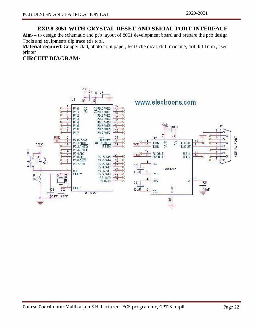
EXP.8 8051 WITH CRYSTAL RESET AND SERIAL PORT INTERFACE Aim--- to design the schematic and pcb layout of 8051 development board and prepare the pcb design
Tools and equipments dip trace eda tool. Material required: Copper clad, photo print paper, fecl3 chemical, drill machine, drill bit 1mm ,laser printer
CIRCUIT DIAGRAM: