electronic transport in graphene nanoribbons and ...rh614yz5124/patrick...electronic transport in...
TRANSCRIPT

Electronic transport in graphene nanoribbons and topological
insulators
Patrick Gallagher
May 2010
Thesis advisor: David Goldhaber-Gordon
Second reader: Aharon Kapitulnik

Abstract
Graphene is an atomically thin sheet of carbon atoms arranged in a honeycomb
lattice. Low-energy electronic excitations in graphene behave like massless Dirac
fermions, and are expected to exhibit exotic phenomena such as relativistic Klein
tunneling.
While the band structure of graphene sheets is gapless, experiments have observed
gap-like behavior in graphene nanoribbons, strips of graphene tens of nanometers
wide. In one part of this thesis, I will present annealing experiments and electronic
transport measurements on nanoribbons of varying lengths and a standardized 30 nm
width. The data support a model in which quantum dots form in series along the
ribbon due to charged impurities, giving rise to the observed gap-like behavior.
Recent theoretical investigations of the effect of spin-orbit coupling in graphene
have led to the discovery of a class of materials known as topological insulators.
A topological insulator is a three-dimensional material which has a band gap for
charge carriers in the bulk, but has gapless surface states protected from disorder
by time-reversal symmetry. A number of novel physical effects are expected in these
materials, such as the formation of Majorana fermions in a topological insulator via
the superconducting proximity effect.
In the second part of this thesis, I will describe an ongoing experiment whose
first goals are to produce thin films of bismuth selenide, a material predicted to be a
topological insulator, and to tune the Fermi level throughout the bulk band gap with
an electrostatic gate. Films as thin as 4 nm can be produced, and show a peak in
resistance as the Fermi level is moved by a gate, perhaps corresponding to the Fermi
level crossing the “Dirac point” of the surface states.
ii
Preface
This thesis summarizes my work since spring 2008 as an undergraduate in Prof. David
Goldhaber-Gordon’s lab at Stanford. I worked on two different projects, which are
described in separate chapters.
Chapter 2 concerns experiments on graphene nanoribbons, which I carried out
between spring 2008 and summer 2009. I produced all of the samples and made all
of the measurements presented here, but I frequently discussed the experiment with
my graduate student mentor, Kathryn Todd, who was finishing her own project on
graphene nanoribbons [1] when I started in the lab. I furthermore inherited several
techniques for graphene fabrication and measurement from Kathryn. It was largely
my decision to focus this project on annealing nanoribbons, but it was Kathryn’s
original suggestion to perform a study of nanoribbons of varying lengths. Note also
that some parts of this chapter, mainly in Sections 2.5 and 2.6, were published in
a paper that I wrote, P. Gallagher et al., Phys. Rev. B 81, 115409 (2010) [2], and
appear in this thesis with only minor modification.
Chapter 3 concerns experiments on topological insulators. I began this project by
myself in spring 2009, and started collaborating on it with a post-doc, James Williams,
who arrived in July 2009. Before James’ arrival, I had developed a process for mak-
ing topological insulator thin films and had made some preliminary low-temperature
transport measurements of my devices. During summer 2009, I trained and super-
vised a high school student intern, Emerson Glassey. I continued to produce all of the
samples for the project, with help from Emerson, while James took over most of the
transport measurement duties. A graduate student, Andrew Bestwick, also joined the
project in fall 2009. Since then, Andrew and I have jointly fabricated the samples for
iii

this experiment. All three of us have been involved in the transport measurements,
although James has done most of the data collection. Bulk crystals for this project
are provided by James Analytis and Jiun-Haw Chu of Ian Fisher’s group at Stanford.
iv

Acknowledgements
I have greatly benefited from my many interactions with students, post-docs, faculty,
friends, and family. Here I will thank just some of the people who have made my
time at Stanford valuable.
The first is my advisor, Prof. David Goldhaber-Gordon. I am indebted to you
for giving me a chance to dig into a research project of relevance to the field. You
are a role model both as a scientist and as a person, and I have learned an incredible
amount from you. Working in your lab has been the highlight of my undergraduate
career. Thanks, David.
Next, I thank Kathryn Todd. Kathryn, thanks for being such a dedicated teacher.
It is hard for me to imagine anyone else being so willing to spend as many hours per
day as you did training an undergraduate who knew absolutely nothing. I had a lot
of fun being in lab with you, and I’m grateful to have worked with you.
Thanks also to Jimmy Williams. You set an example for everyone with your hard
work. It’s a pleasure to do science with you, and I have learned a whole lot from you.
Thank you, Andrew Bestwick, for educating me about 80s movies while we pro-
cessed samples. Thanks to Emerson Glassey for helping with sample fabrication in
the summer, to Sami for being “Dr. Dot,” to Andrei for the ski jump, to Markus for
saving my nitrogen transfers, to Joey for always fixing our SEM, to Nimrod for being
a supportive yet demanding 108 TA, and to the other members of the Goldhaber-
Gordon lab. I’ve enjoyed interacting with all of you.
Thanks also to Prof. Aharon Kapitulnik for an enjoyable quarter of Physics 108
and for reading this thesis.
For discussions about graphene nanoribbon physics, I thank Gil Refael, Antonio
v

Castro Neto, Eduardo Mucciolo, Misha Fogler, Enrico Rossi, and Shaffique Adam.
Finally, thanks to my parents, Timothy and Vijaya, and my sister, Shamala.
Without your support I would not have come this far.
vi

Contents
Preface iii
Acknowledgements v
1 Introduction 1
2 Graphene nanoribbons 3
2.1 Background . . . . . . . . . . . . . . . . . . . . . . . . . . . . . . . . 3
2.2 Overview of experiment . . . . . . . . . . . . . . . . . . . . . . . . . 10
2.3 Sample fabrication . . . . . . . . . . . . . . . . . . . . . . . . . . . . 14
2.4 Measurement process . . . . . . . . . . . . . . . . . . . . . . . . . . . 18
2.5 Aggregate annealing results . . . . . . . . . . . . . . . . . . . . . . . 21
2.6 Few-dot Coulomb blockade . . . . . . . . . . . . . . . . . . . . . . . . 26
2.7 Conclusions . . . . . . . . . . . . . . . . . . . . . . . . . . . . . . . . 32
3 Topological insulators 35
3.1 Background . . . . . . . . . . . . . . . . . . . . . . . . . . . . . . . . 35
3.2 Overview of experiment . . . . . . . . . . . . . . . . . . . . . . . . . 40
3.3 Sample fabrication . . . . . . . . . . . . . . . . . . . . . . . . . . . . 41
3.4 Carrier density measurements . . . . . . . . . . . . . . . . . . . . . . 43
3.5 Resistance peak in top-gated samples . . . . . . . . . . . . . . . . . . 46
3.6 Weak antilocalization . . . . . . . . . . . . . . . . . . . . . . . . . . . 51
3.7 Controlling sample doping . . . . . . . . . . . . . . . . . . . . . . . . 53
3.8 Conclusions . . . . . . . . . . . . . . . . . . . . . . . . . . . . . . . . 55
vii

Bibliography 56
viii
Chapter 1
Introduction
Graphene is an atomically thin sheet of carbon atoms arranged in a honeycomb
lattice. A tight-binding calculation reveals an unusual band structure: graphene is a
semimetal, and for low energies the dispersion relation is linear. In principle, then,
graphene provides an opportunity to study massless Dirac fermions in a solid state
system.
Calculations of graphene’s band structure were first published in the 1940s [3], but
at the time it was thought that a truly two-dimensional material like graphene would
not be stable [4]. Yet in 2004, the first paper reporting the experimental isolation
of graphene was published [5], and since then the scientific community has seen an
explosion of interest in this material. Graphene shows promise not only as a means of
exploring new physics, but also as a platform for new technology; for instance, due to
graphene’s high carrier mobility, nearly linear current-voltage relationship, small size,
and ability to sustain large currents, some have suggested that graphene could be
used to make small, efficient, high-frequency transistors for analog signal processing
[5, 6].
One might also imagine patterning a graphene sheet into transistors for logic
operations. The roadblock to making this sort of graphene-based computer chip
is the lack of a band gap in graphene, which leads to smaller on/off conductance
ratios than in semiconductor transistors. But in 2007, the first experiments were
published that revealed that when graphene is cut into nanoribbons, strips of graphene
1

CHAPTER 1. INTRODUCTION 2
of nanometer-scale width, gap-like behavior is produced [7]. Substantial theoretical
and experimental attention has since been focused on graphene nanoribbons, but
the exact origin of this gap-like behavior in the disordered samples produced in the
laboratory is still not fully understood. Chapter 2 of this thesis is devoted to my own
experimental investigation of the origin of this gap-like behavior.
Shortly after the rise of graphene, a series of theoretical predictions [8, 9, 10, 11, 12]
suggested the existence of a new class of materials called topological insulators, whose
electronic properties are related to those of graphene. Topological insulators are three-
dimensional crystals with an energy gap for bulk states, like ordinary insulators.
However, within the bulk energy gap, there exist states on the surface of the crystal
which are gapless. The metallic nature of these states is protected from strong disorder
by time-reversal symmetry. Angle-resolved photoemission spectroscopy (ARPES) and
scanning tunneling microscopy (STM) experiments [13, 14, 15, 16, 17, 18, 19, 20, 21]
have confirmed theoretical predictions [22, 23] about the band structure of materials
proposed to be topological insulators, including Bi1−xSbx, Bi2Se3, Bi2Te3, and Sb2Te3.
Topological insulators, like graphene, have technological potential. Proposals exist
for harnessing the properties of the surface states to build new spintronic devices
and topological quantum computers [24, 25]. For micro- and nano-electronic devices
devices to be realized, the Fermi level must be tuned to the bulk gap. Such tunability
in solid state systems is often accomplished with an electrostatic gate. But there
is a practical limit to the voltage that can be placed on the gate, and thus to the
amount of tunability that the gate provides; in order for the gate to be effective, the
topological insulator film must be thin (on the order of nanometers) to create a large
surface to volume ratio. Chapter 3 of this thesis describes experiments to produce
gate-responsive thin films of topological insulators.

Chapter 2
Graphene nanoribbons
2.1 Background
The band structure of graphene for low energies consists of conical conduction and
valence bands that meet with zero gap at the K and K’ points at the corners of the
first Brillouin zone (see Figure 2.1) [3]. Low-energy excitations can be described by
spinor solutions to a Dirac Hamiltonian in two spatial dimensions,
H = −ihvFσ · ∇,
where σ = (σx, σy) are the Pauli matrices and vF ≈ 106 m/s is the Fermi velocity. In
this case, the two components of the spinor solutions do not correspond to probability
amplitudes for spin up and spin down, but rather to probability amplitudes on the
two different hexagonal sublattices that make up graphene’s honeycomb lattice [4].
The electronic properties of graphene nanoribbons, however, in general differ from
those of a 2-d sheet due to a nanoribbon’s finite width. At liquid helium temperatures
(near 4 K), transport experiments on graphene sheets of several microns in length and
width typically reveal a minimum conductivity of a few times e2/h per square [26].
(The “conductance quantum” e2/h is best known as the conductance contribution of
one carrier type in a perfect 1D wire; a 2D conductivity, or conductance per square,
3

CHAPTER 2. GRAPHENE NANORIBBONS 4
(a) (b)
(c)
Figure 2.1: (a) Graphene lattice. Yellow and blue circles correspond to atoms ofthe two hexagonal sublattices that together form the honeycomb lattice. (b) FirstBrillouin zone of graphene, showing symmetry points. (c) Energy bands of graphene.The valence and conduction bands touch at the “Dirac points” (at zero energy andat the K and K’ points in k-space) to form zero-gap Dirac cones. Figures taken fromCastro Neto et al. [4].

CHAPTER 2. GRAPHENE NANORIBBONS 5
of e2/h is significant in a variety of contexts other than graphene, such as 2D metal-
insulator transitions [27].) In contrast, conductance of graphene nanoribbon devices
at temperatures around 4 K is typically suppressed orders of magnitude below e2/h
for a large range of Fermi energies, even in ribbons only several squares long. An
example of this behavior, reminscent of a band gap, is shown in Figure 2.2. It is not
obvious, however, that this conductance suppression is the result of an energy gap
between electrons and holes in the band structure of a graphene nanoribbon.
Theoretical analyses suggest that graphene nanoribbons can indeed be semicon-
ducting. But their exact electronic properties turn out to be very sensitive to the
boundary conditions chosen for the electronic wavefunction. For example, Figure 2.3
shows the two ideal edge configurations, called “armchair” and “zigzag,” of a graphene
nanoribbon, where edge passivation by non-carbon elements has been ignored. As-
sume boundary conditions such that the electronic wavefunction vanishes on all edge
sites of an armchair ribbon and on the outermost sublattice on the edges of a zigzag
ribbon. Tight-binding calculations and solutions of graphene’s Dirac equation subject
to these boundary conditions both reveal that zigzag ribbons are metallic. On the
other hand, armchair ribbons are typically semiconducting due to quantum confine-
ment effects, although armchair ribbons whose widths are integer multiples of 3 times
the graphene lattice constant are metallic [28]. These results furthermore change
substantially if the carbon atoms on the edge are passivated with hydrogen atoms;
theoretical studies find that hydrogen-passivated zigzag and armchair GNRs are both
semiconducting, although the gap sizes and physics underlying the formation of the
gaps differ for different edge configurations [29, 30].
Laboratory measurements of the electronic properties of graphene nanoribbons are
typically carried out on ribbons etched from graphene sheets using a lithographically-
defined etch mask. As a result, the edges of these ribbons are highly disordered, and
predictions that assume ideal ribbon edges need not apply to data such as those shown
in Figure 2.2, especially given the sensitivity of the results to boundary conditions.
Calculations that incorporate disorder into the edge structure in fact find that even
slight deviations from perfect edge structure lead to localized states (a phenomenon

CHAPTER 2. GRAPHENE NANORIBBONS 6
5 10 15 20 25 30 35 40 45 500
0.01
0.02
0.03
0.04
0.05
0.06
0.07
0.08
Back gate voltage (V)
Con
duct
ance
(2e
2 /h)
Figure 2.2: Conductance versus back gate voltage at 4 K for a 1.6 µm long, 30 nmwide graphene nanoribbon that I fabricated. The back gate voltage controls theFermi energy: the voltage is linearly proportional to the carrier density in the ribbon.Between 20 and 30 V on the back gate, the conductance drops to zero, as would beexpected for a material tuned into a band gap.
Armchair edge
Zigz
ag e
dge
Figure 2.3: A graphene lattice displaying ideal armchair edges on the bottom andtop, and ideal zigzag edges on the left and right. Taken with slight modification fromCastro Neto et al. [4].
CHAPTER 2. GRAPHENE NANORIBBONS 7
VG
VSD
Gate
Source DrainIsland
Tun
nel
bar
rier
Tun
nel
bar
rier
Figure 2.4: Schematic diagram of a quantum dot system. The island is coupled bytunnel barriers to source and drain reservoirs, and is also capacitively coupled to agate electrode at voltage VG. In general, the source and drain reservoirs can havesome potential difference VSD.
known as Anderson localization) and gap-like transport behavior [31]. These calcula-
tions agree qualitatively with early experimental studies of gap behavior in graphene
nanoribbons: both theory and experiment find that the apparent “energy gap” scales
roughly as 1/(W −W0), where W is the nanoribbon width and W0 is a constant [7].
But this qualitative agreement is not convincing evidence that Anderson localiza-
tion physics is the most relevant in understanding lithographically-produced nanorib-
bons. The magnitude of the gap determined by the calculation is still 10 times larger
than that found in the experiments. Furthermore, more recent experimental studies
[32, 1, 33, 34] have noted signatures of quantum dot behavior in graphene nanorib-
bons, suggesting another possible explanation for the gap features.
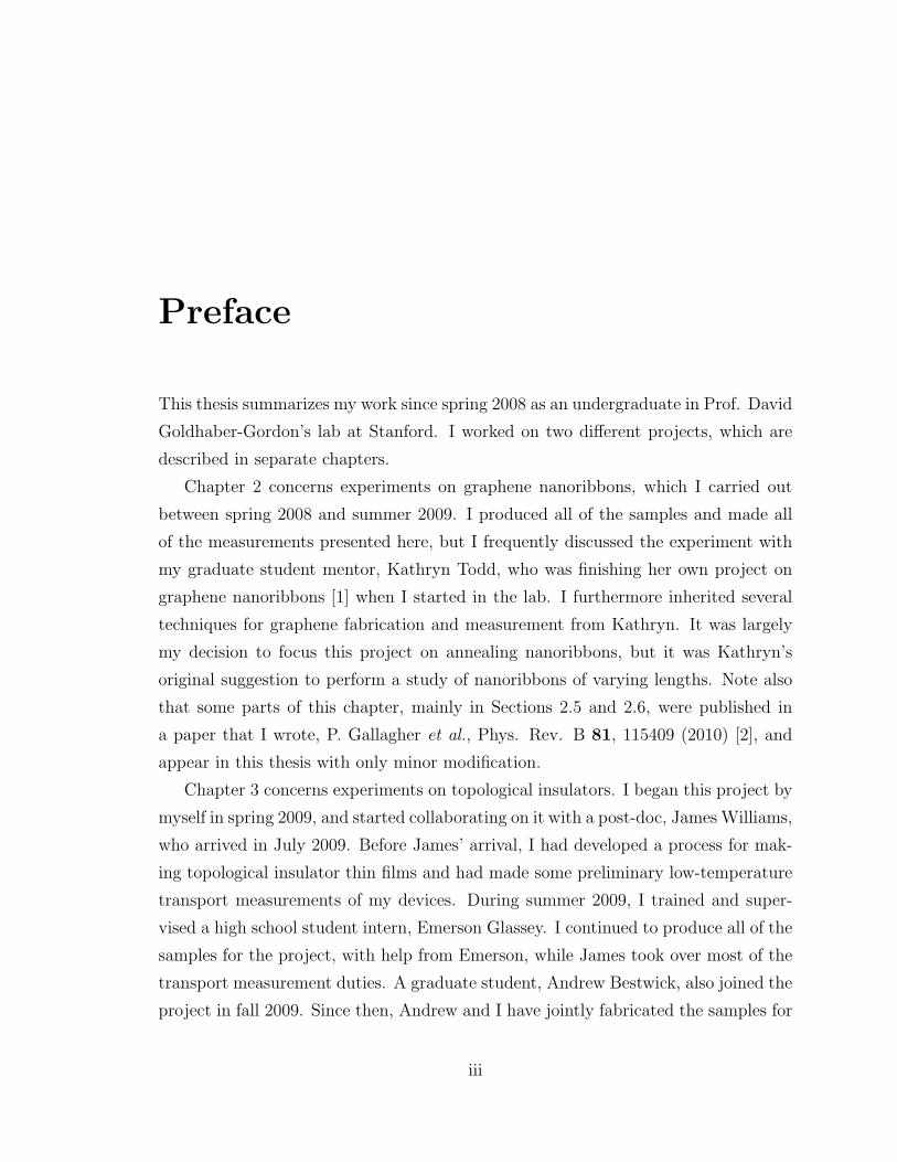
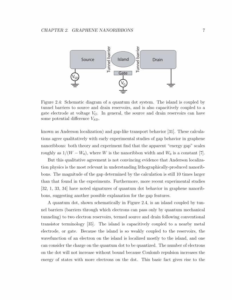
A quantum dot, shown schematically in Figure 2.4, is an island coupled by tun-
nel barriers (barriers through which electrons can pass only by quantum mechanical
tunneling) to two electron reservoirs, termed source and drain following conventional
transistor terminology [35]. The island is capacitively coupled to a nearby metal
electrode, or gate. Because the island is so weakly coupled to the reservoirs, the
wavefunction of an electron on the island is localized mostly to the island, and one
can consider the charge on the quantum dot to be quantized. The number of electrons
on the dot will not increase without bound because Coulomb repulsion increases the
energy of states with more electrons on the dot. This basic fact gives rise to the
CHAPTER 2. GRAPHENE NANORIBBONS 8
transport behavior of the quantum dot, known as Coulomb blockade: a current can
flow through the dot only when energy levels align such that the number of electrons
on the dot can fluctuate.
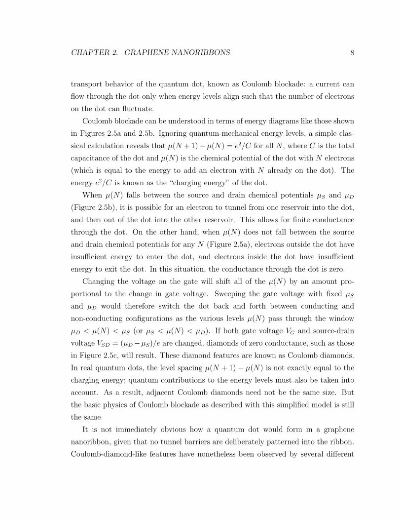
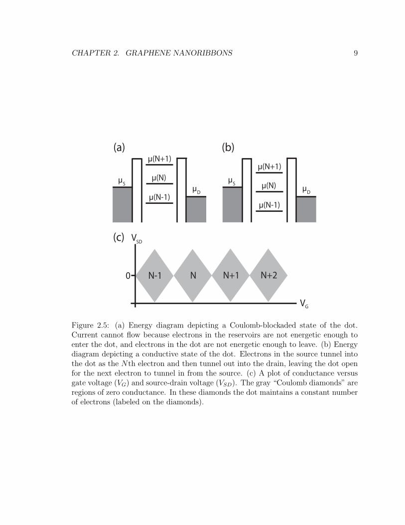
Coulomb blockade can be understood in terms of energy diagrams like those shown
in Figures 2.5a and 2.5b. Ignoring quantum-mechanical energy levels, a simple clas-
sical calculation reveals that µ(N + 1)− µ(N) = e2/C for all N , where C is the total
capacitance of the dot and µ(N) is the chemical potential of the dot with N electrons
(which is equal to the energy to add an electron with N already on the dot). The
energy e2/C is known as the “charging energy” of the dot.
When µ(N) falls between the source and drain chemical potentials µS and µD
(Figure 2.5b), it is possible for an electron to tunnel from one reservoir into the dot,
and then out of the dot into the other reservoir. This allows for finite conductance
through the dot. On the other hand, when µ(N) does not fall between the source
and drain chemical potentials for any N (Figure 2.5a), electrons outside the dot have
insufficient energy to enter the dot, and electrons inside the dot have insufficient
energy to exit the dot. In this situation, the conductance through the dot is zero.
Changing the voltage on the gate will shift all of the µ(N) by an amount pro-
portional to the change in gate voltage. Sweeping the gate voltage with fixed µS
and µD would therefore switch the dot back and forth between conducting and
non-conducting configurations as the various levels µ(N) pass through the window
µD < µ(N) < µS (or µS < µ(N) < µD). If both gate voltage VG and source-drain
voltage VSD = (µD−µS)/e are changed, diamonds of zero conductance, such as those
in Figure 2.5c, will result. These diamond features are known as Coulomb diamonds.
In real quantum dots, the level spacing µ(N + 1)− µ(N) is not exactly equal to the
charging energy; quantum contributions to the energy levels must also be taken into
account. As a result, adjacent Coulomb diamonds need not be the same size. But
the basic physics of Coulomb blockade as described with this simplified model is still
the same.
It is not immediately obvious how a quantum dot would form in a graphene
nanoribbon, given that no tunnel barriers are deliberately patterned into the ribbon.
Coulomb-diamond-like features have nonetheless been observed by several different
CHAPTER 2. GRAPHENE NANORIBBONS 9
µ(N+1)
µ(N)
µ(N-1)
µS
µD
µ(N+1)
µ(N)
µ(N-1)
µS
µD
(a) (b)
V
VSD
G
0 N-1 N N+1 N+2
(c)
Figure 2.5: (a) Energy diagram depicting a Coulomb-blockaded state of the dot.Current cannot flow because electrons in the reservoirs are not energetic enough toenter the dot, and electrons in the dot are not energetic enough to leave. (b) Energydiagram depicting a conductive state of the dot. Electrons in the source tunnel intothe dot as the Nth electron and then tunnel out into the drain, leaving the dot openfor the next electron to tunnel in from the source. (c) A plot of conductance versusgate voltage (VG) and source-drain voltage (VSD). The gray “Coulomb diamonds” areregions of zero conductance. In these diamonds the dot maintains a constant numberof electrons (labeled on the diamonds).

CHAPTER 2. GRAPHENE NANORIBBONS 10
groups [32, 1, 33, 34]. For shorter ribbons, these diamonds can be clearly resolved, and
the pattern of diamonds resembles that of a few quantum dots in parallel and/or in
series. For longer ribbons, the diamonds of suppressed conductance start overlapping,
as expected for multiple dots in series [36]. These observations suggest that charge
transport could be occurring through an arrangement of quantum dots along the
ribbon.
It has been proposed that quantum dots form as a result of lithographic line-edge
roughness: the width of the nanoribbon is assumed to narrow at several locations,
strongly reducing the number of conducting channels and thereby providing a “tun-
nel barrier” that defines quantum dots [37]. Alternatively, quantum dots could form
as a result of potential inhomogeneities. It has been demonstrated theoretically [38]
and experimentally [39] that the transport properties of extended graphene sheets
are governed by charged impurity scattering, and that the potential of the sheet has
substantial spatial variation on even the length scale of a few nanometers, leading to
adjacent n and p regions when the sheet is near net charge neutrality [23]. Nanorib-
bons likely also have a disorder potential, and thus adjacent n and p regions, due to
charged impurities near the ribbon. However, if electrons in graphene are governed
by the Dirac-like Hamiltonian derived from tight-binding calculations, they should
exhibit relativistic Klein tunneling: near-perfect transmission through appropriately
sized energy barriers for a range of incident angles [40]. As a result, adjacent n and
p regions need not cause localization.
But if there existed a small energy gap between electrons and holes in the nanorib-
bon, perhaps induced by quantum confinement, “tunnel barrier” regions of zero charge
carrier density could arise between regions of n and p, resulting in isolated puddles
of charge carriers along the ribbon which behave as quantum dots [32, 1].
2.2 Overview of experiment
The goal of my project was to shed light on the mechanism responsible for the gap-like
behavior in graphene nanoribbons. In particular, I hoped to determine which of the
multiple plausible models, including those based on Anderson localization due to edge
CHAPTER 2. GRAPHENE NANORIBBONS 11
defects and those based on Coulomb blockade due to edge roughness or charged impu-
rities, most adequately describes the behavior of lithographically-produced graphene
nanoribbons.
What kinds of experiments could distinguish between these various models? In-
dependently tuning the strengths of the different types of disorder and observing the
gap properties is one possibility. Long-range scattering, as from charged impurities in
the vicinity of the graphene, is not predicted to cause Anderson localization in either
extended graphene sheets or nanoribbons [41, 42, 43, 44], while short-range scatterers
such as lattice defects are expected to contribute to Anderson localization. Thus, an
experiment that changed the concentration of long-range scatterers but not short-
range scatterers could provide evidence for or against Anderson localization theories.
Charged impurities can be selectively removed without modifying the edge structure
by annealing the nanoribbons at temperatures low enough to prevent restructuring of
the lattice but high enough to desorb contaminants. A substantial part of my work
is devoted to such annealing experiments.
Data from basic transport experiments also provide useful information for distin-
guishing between models. In the picture of potential inhomogeneities in conjunction
with a small confinement gap creating a serial arrangement of quantum dots, we
expect to find two distinct “gaps” in the conductance data. First, note that the
quantum dot behavior is only apparent when the Fermi level is close enough to the
charge neutrality point (the point at which the charge density averaged over all pud-
dles is zero) that the carrier density varies spatially from electron-like to hole-like
(see Figure 2.6), since otherwise there will be no tunnel barriers between puddles to
form quantum dots. Thus the “transport gap,” the region of suppressed conductance
at zero source-drain bias, is given approximately by the disorder amplitude plus the
confinement gap. The second gap is the “source-drain gap,” which is roughly the
largest value of source-drain bias for which conductance is suppressed at some EF .
The size of this gap is not determined by the size of the transport gap. In the simplest
case of single-dot transport, the source-drain gap is the charging energy of the dot,
which need not have a clear dependence on the disorder amplitude. In the case of
multiple quantum dots, determining the source-drain gap is more complicated, but

CHAPTER 2. GRAPHENE NANORIBBONS 12
Energy
EF
Position
Tran
spor
t gap
Confinementgap
Figure 2.6: Cartoon of quantum dots forming along the ribbon due to potentialinhomogeneities and a confinement gap. The red puddles indicate electrons, and theblue puddles indicate holes. The thick dark curves on the top diagram depict theenergies of the bottom of the conduction band and the top of the valence band as afunction of position along the dashed line on the cartoon below. The curve splits intotwo inside the ribbon because of the confinement gap. The “transport gap” can beidentified as the amplitude of the disorder plus the confinement gap.

CHAPTER 2. GRAPHENE NANORIBBONS 13
we still expect the source-drain gap to depend on the particular shape of the disorder
potential, and the shape of the disorder potential is not strongly constrained by its
amplitude.
My experiment consisted of fabricating graphene nanoribbon samples of a constant
30 nm width and of lengths varying from 30 to 3000 nm, and observing their gap
behavior at low temperatures before and after annealing. My data most stongly
support the theory that quantum dots form in series along the ribbon as a result of
potential inhomogeneities, leading to substantial conductance suppression in a long
enough ribbon.
The most important findings, which I will discuss in further detail in the following
sections, are as follows. First, by considering the effect of annealing nanoribbons to
remove bulk impurities, I find that the source-drain and transport gaps cannot be
predicted on the basis of geometry alone. The gap properties appear to strongly
depend on the particular arrangement of bulk impurities. Second, my data show that
the transport gap varies independently from the source-drain gap, in contrast with
the results of previous work [34], and that the transport gap decreases with annealing,
as expected within the charged-impurity-induced quantum dot model since annealing
should reduce the disorder amplitude. Third, similarly to the findings of studies on
extended graphene sheets [39], my data reveal a connection between the transport
gap size and its distance from zero volts in backgate, suggesting that the transport
gap is a measure of the doping of the sample; the doping is likely connected to the
disorder amplitude. Fourth, data on the relationship between source-drain gap and
ribbon length indicate that in general longer ribbons have larger gaps, although the
scatter in these data is substantial. Finally, measurements on a particular ribbon
sample show very periodic conductance oscillations that strongly suggest that the
resonances commonly observed in nanoribbon measurements result from Coulomb
blockade effects instead of Anderson localization effects.

CHAPTER 2. GRAPHENE NANORIBBONS 14
5 µm
single layer
multi-layer
Figure 2.7: Optical microscope photograph of a graphene flake on SiO2. The flakeon the left is single layer graphene, and the flake on the right is multi-layer (likelybilayer).
2.3 Sample fabrication
Fabrication of graphene nanoribbons is typically accomplished by depositing an ex-
tended graphene flake on SiO2, covering certain areas of the flake with an etch mask,
and selectively etching away parts of the flake to leave a nanoribbon structure. This
is the technique that I have also used to fabricate my devices, although I have devel-
oped a new etch mask technique that was better-suited to my experiment than were
the typical masking methods.
The graphene sheets that I used for my experiments were produced by the proce-
dure pioneered by Novosolov et al. in 2004 [5]. Macroscopic crystals of natural Kish
graphite are placed on Scotch tape and peeled repeatedly. Due to the weak bonding
between layers in graphite, the repeated peeling thins the initial crystal down sub-
stantially. Once the tape is covered in a very thin layer of graphite, it is pressed down
onto a 5 mm by 5 mm n-doped silicon substrate coated with 300 nm of thermal SiO2.
The tape is peeled off of the chip, leaving behind very thin graphite flakes that cling
to the oxide surface.
Single-atomic-layer graphene flakes can be identified on the SiO2 (and distin-
guished from bilayer or thicker flakes) using an ordinary optical microscope provided
that the thickness of the underlying SiO2 is carefully selected. A photograph of one
CHAPTER 2. GRAPHENE NANORIBBONS 15
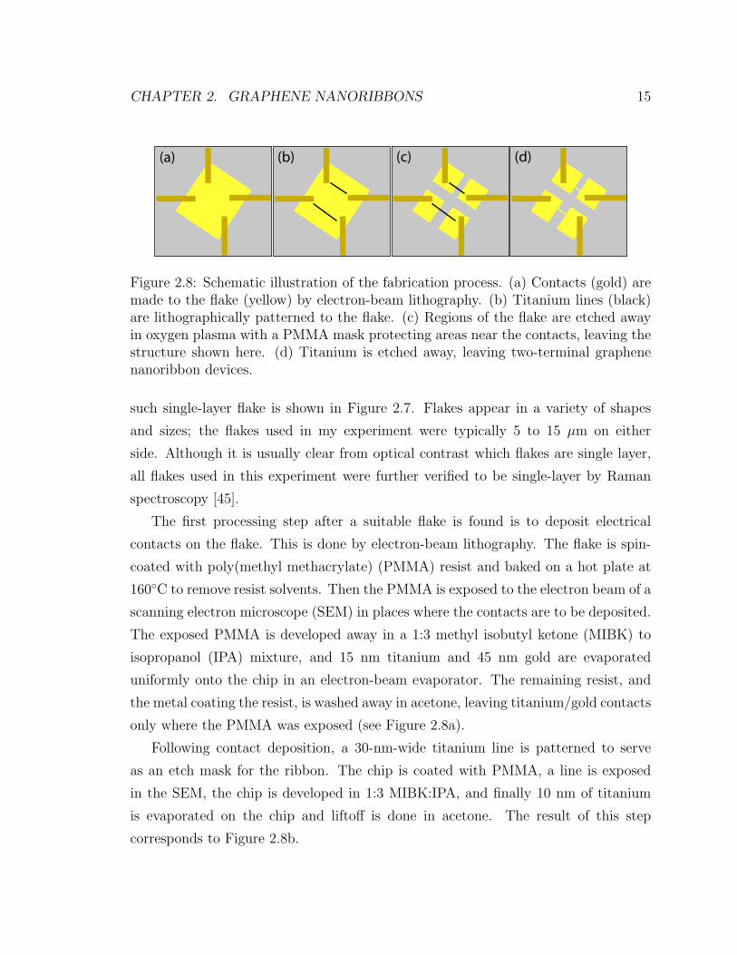
(a) (b) (c) (d)
Figure 2.8: Schematic illustration of the fabrication process. (a) Contacts (gold) aremade to the flake (yellow) by electron-beam lithography. (b) Titanium lines (black)are lithographically patterned to the flake. (c) Regions of the flake are etched awayin oxygen plasma with a PMMA mask protecting areas near the contacts, leaving thestructure shown here. (d) Titanium is etched away, leaving two-terminal graphenenanoribbon devices.
such single-layer flake is shown in Figure 2.7. Flakes appear in a variety of shapes
and sizes; the flakes used in my experiment were typically 5 to 15 µm on either
side. Although it is usually clear from optical contrast which flakes are single layer,
all flakes used in this experiment were further verified to be single-layer by Raman
spectroscopy [45].
The first processing step after a suitable flake is found is to deposit electrical
contacts on the flake. This is done by electron-beam lithography. The flake is spin-
coated with poly(methyl methacrylate) (PMMA) resist and baked on a hot plate at
160C to remove resist solvents. Then the PMMA is exposed to the electron beam of a
scanning electron microscope (SEM) in places where the contacts are to be deposited.
The exposed PMMA is developed away in a 1:3 methyl isobutyl ketone (MIBK) to
isopropanol (IPA) mixture, and 15 nm titanium and 45 nm gold are evaporated
uniformly onto the chip in an electron-beam evaporator. The remaining resist, and
the metal coating the resist, is washed away in acetone, leaving titanium/gold contacts
only where the PMMA was exposed (see Figure 2.8a).
Following contact deposition, a 30-nm-wide titanium line is patterned to serve
as an etch mask for the ribbon. The chip is coated with PMMA, a line is exposed
in the SEM, the chip is developed in 1:3 MIBK:IPA, and finally 10 nm of titanium
is evaporated on the chip and liftoff is done in acetone. The result of this step
corresponds to Figure 2.8b.

CHAPTER 2. GRAPHENE NANORIBBONS 16
Figure 2.9: Electron micrograph in false color of a typical device, of length 900 nmand width 30 nm (scale bar: 500 nm). Two metal leads (top, bottom) are connectedto graphene leads that ultimately contact the nanoribbon. A faint dark line can beseen extending from the ribbon into the leads; this is a small amount of residue fromthe titanium mask (see text for discussion). Image taken at 5.0 kV on a FEI XL30Sirion SEM.
A final SEM exposure is then used to complete the etch mask. The chip is again
coated with PMMA and windows are opened up in the PMMA around the titanium
lines. The whole chip is then exposed to an oxygen plasma etch for 8 seconds at 65
W, which removes any unprotected graphene. After the plasma etch, the chip looks
like Figure 2.8c. Finally, the chip is immersed in 30% hydrochloric acid at 85C for
30 minutes to etch the titanium, and the PMMA mask on the leads is then removed
in acetone (the HCl penetrates under the PMMA mask so that parts of the titanium
mask still covered by the PMMA are also removed). The final product is shown
schematically in Figure 2.8d. An SEM micrograph of a typical device is shown in
Figure 2.9.
Several previous experiments have used PMMA as an etch mask to define the
ribbons [32, 1, 33, 34]. However, PMMA itself gets etched by oxygen plasma at a
significant rate in all directions, which makes the etching time critical in determining

CHAPTER 2. GRAPHENE NANORIBBONS 17
the ribbon width. Controlling the etching time to the precision required to produce
samples of constant width is difficult. Other experiments have used HSQ, a negative
resist which becomes silica upon electron-beam exposure, to define an etch mask
[7, 46]. This circumvents the difficulties of controlling the ribbon width, but the
silica mask is very challenging to remove without destroying the device, which is
problematic for my purposes: to perform an annealing experiment, one of the ribbon
surfaces should be uncovered so that impurities can be desorbed.
The titanium etch mask technique is thus useful because it allows for accurate
width control and it is relatively easy to remove without damaging the graphene
below. The downside to this technique, however, is that invariably there is some
residue from the etch mask (perhaps an oxide) which is faintly observable in the SEM
(see Figure 2.9). There is sometimes a small AFM signal when attempting to measure
this residue, but it is difficult to get an accurate height estimate when the material
being measured (the residue) is different from the surrounding material (graphene).
Although it appears that any residual mask material is not affecting transport
properties, since the ribbons made by this process behave similarly to those made by
other lithographic processes, I performed several tests to gain further information.
First, I prepared a graphene Hall bar sample, coated part of it in titanium and then
etched away the titanium using the same process as was used for the nanoribbons.
Four-terminal conductance measurements revealed characteristic graphene behavior
before the titanium etch mask was deposited and after it was removed, with a mo-
bility degradation of the degree expected from additional lithography: the mobility
decreased from 6000 cm2V−1s−1 to 800 cm2V−1s−1 after titanium deposition and
removal. A bulk mobility of 800 cm2V−1s−1 is typical for the nanoribbon devices
fabricated previously by other members of this research group using two steps of
lithography with no titanium deposition or titanium etch [1]. Raman spectroscopy
revealed no changes in the disorder peak after the titanium deposition and removal,
and the Raman spectrum did not reveal any differences between the parts of the
flake that were once covered with titanium and the parts that were not covered with
titanium.
Auger measurements using a PHI 700 found no residual titanium to within the

CHAPTER 2. GRAPHENE NANORIBBONS 18
sensitivity of the instrument: the titanium signal was the same on all parts of the
devices studied, regardless of whether or not titanium had been deposited there to
begin with. Based on Auger measurements of a titanium film of known thickness,
I estimate that any residual titanium film on the nanoribbons is less than 0.2 nm
thick. While this upper bound is rather large, given all the evidence presented here,
it appears that the titanium mask is being sufficiently removed by the etch process
and that the amount of residual titanium on the ribbons is well below this upper
bound.
2.4 Measurement process
All measurements reported in this chapter were performed at 4.2 to 4.4 K in a cryostat
in vacuum, or at 4.2 K while immersed in liquid helium at atmospheric pressure. Cryo-
genic temperatures are desirable because the gap properties of graphene nanoribbons
are obscured at high temperatures by thermal broadening. The Coulomb-diamond-
like features, for example, which provide important insights into the physics governing
the gap behavior, cannot be distinguished at room temperature.
In total, I took data on 21 different nanoribbons, about half of which were an-
nealed. A typical annealing process involved taking data at low temperature, warming
up to room temperature to anneal the sample, and cooling back down to take data
again and observe the change. I used two different methods of annealing that have
been reported to remove surface impurities in extended graphene sheets: annealing of
the whole chip in argon at 300C [47], and current annealing in vacuum, which heats
an individual ribbon by Joule heating [48, 49]. The whole-chip annealing consisted
of removing the sample from the cryostat, exposing it to atmosphere, annealing in a
furnace, and exposing the sample to atmosphere again to put back in to the cryostat.
Current annealing was done without breaking vacuum in the cryostat. A summary
of all the samples measured and their annealing histories is given in Table 2.1.
Data collection was done with standard low-noise techniques. A lockin amplifier
puts a small, slowly-oscillating voltage of amplitude ∆V on the source lead. A current
pre-amplifier (input at zero voltage) is attached to the drain lead. The pre-amplifier
CHAPTER 2. GRAPHENE NANORIBBONS 19
Data set Annealing history
A Not annealed; data taken while immersed in liquid heliumB Not annealed; data taken while immersed in liquid heliumC1 Not annealed; data taken while immersed in liquid heliumC2 Removed from cryostat after C1, argon annealed at 300C,
exposed to atmosphere, cooled down; data taken in vacuumC3 Warmed to RT after C2, current annealed in vacuum at ∼ 3× 10⁸
A/cm2, cooled down (without breaking vacuum since C2)D1 Not annealed; data taken in vacuumD2 Exposed to atmosphere after D1, current annealed in vacuum at
∼ 5× 10⁷ A/cm2, cooled down; data taken in vacuumD3 Warmed to RT after D2, current annealed in vacuum at ∼ 3× 10⁸
A/cm2, cooled down (without breaking vacuum since D2)E Not annealed; data taken in vacuum
Table 2.1: Description of data set labels for the samples considered in this work. Datasets are named with a letter and sometimes a number; sets of the same letter but withdifferent numbers correspond to the same group of ribbons on successive cooldowns,following successive anneals. Note that each data set can contain multiple ribbons.Current densities are calculated assuming a sheet thickness of 0.35 nm, consistentwith previous work [48].

CHAPTER 2. GRAPHENE NANORIBBONS 20
converts its slowly-oscillating input current, of amplitude ∆I, into a slowly-oscillating
voltage whose amplitude is read by the lockin. The differential conductance can then
be calculated as dI/dV ≈ ∆I/∆V . A dc voltage can also be placed on the source
lead in addition to the ac excitation from the lockin in order to measure dI/dV at
different source-drain biases. A final voltage source is attached to the heavily n-doped
silicon substrate (the “back gate”), separated from the graphene by the 300 nm SiO2
layer, to capacitively control the charge carrier density (and hence the Fermi level)
in the graphene. Data collection then consists of measuring dI/dV at various values
of back gate voltage and source-drain voltage.
The key pieces of information extracted from a nanoribbon on a given cooldown
are the source-drain and transport gaps. For ease of comparison to other work, trans-
port gaps are calculated by the method introduced by Molitor et al. [34]. Using
the zero-bias cut of conductance versus gate voltage (as shown in Figure 2.2), a line
is fit to the regions surrounding the zero-conductance region where conductance in-
creases approximately linearly with gate voltage. The linear fits are extrapolated to
zero conductance, and the transport gap is defined as the voltage difference between
the two zero-crossings. The “source-drain gap” is found by first smoothing the data
using a 0.5 V window in back gate voltage. The source-drain gap is then identified
as the largest source-drain voltage below which, for both positive and negative bi-
ases, the (smoothed) differential resistance exceeds 5 MΩ for some back gate voltage.
The smoothing step is included because there are often one or two outlying “spike”
features for which the resistance exceeds 5 MΩ over a range of source-drain voltages
much larger than the typical “gap” source-drain voltage near the charge neutrality
point; these features have a very small width in back gate voltage (∼ 0.1 V) and are
washed out by the smoothing. While it is possible to choose different and equally
valid definitions of the transport and source-drain gaps, any one definition applied
consistently across the data sets allows meaningful statements to be made about the
variation of these quantities with ribbon geometry. As was found by Molitor et al.
[34], the precise gap definitions used do not change the general features of the results.
CHAPTER 2. GRAPHENE NANORIBBONS 21
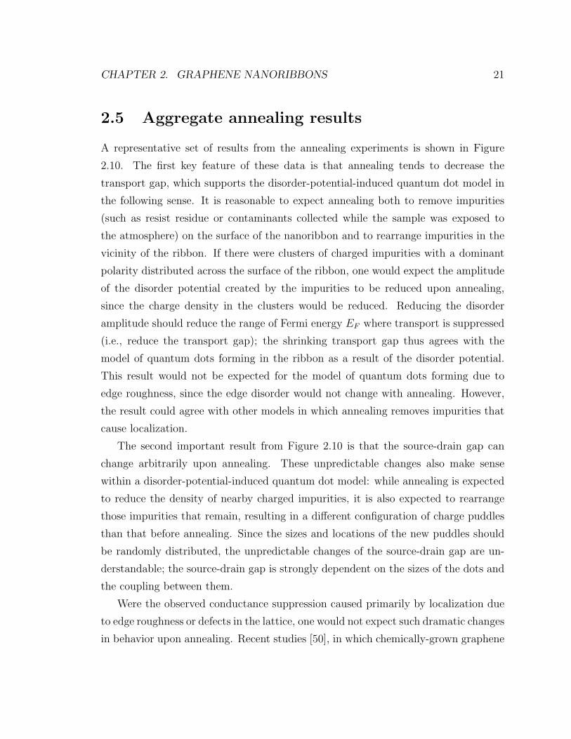
2.5 Aggregate annealing results
A representative set of results from the annealing experiments is shown in Figure
2.10. The first key feature of these data is that annealing tends to decrease the
transport gap, which supports the disorder-potential-induced quantum dot model in
the following sense. It is reasonable to expect annealing both to remove impurities
(such as resist residue or contaminants collected while the sample was exposed to
the atmosphere) on the surface of the nanoribbon and to rearrange impurities in the
vicinity of the ribbon. If there were clusters of charged impurities with a dominant
polarity distributed across the surface of the ribbon, one would expect the amplitude
of the disorder potential created by the impurities to be reduced upon annealing,
since the charge density in the clusters would be reduced. Reducing the disorder
amplitude should reduce the range of Fermi energy EF where transport is suppressed
(i.e., reduce the transport gap); the shrinking transport gap thus agrees with the
model of quantum dots forming in the ribbon as a result of the disorder potential.
This result would not be expected for the model of quantum dots forming due to
edge roughness, since the edge disorder would not change with annealing. However,
the result could agree with other models in which annealing removes impurities that
cause localization.
The second important result from Figure 2.10 is that the source-drain gap can
change arbitrarily upon annealing. These unpredictable changes also make sense
within a disorder-potential-induced quantum dot model: while annealing is expected
to reduce the density of nearby charged impurities, it is also expected to rearrange
those impurities that remain, resulting in a different configuration of charge puddles
than that before annealing. Since the sizes and locations of the new puddles should
be randomly distributed, the unpredictable changes of the source-drain gap are un-
derstandable; the source-drain gap is strongly dependent on the sizes of the dots and
the coupling between them.
Were the observed conductance suppression caused primarily by localization due
to edge roughness or defects in the lattice, one would not expect such dramatic changes
in behavior upon annealing. Recent studies [50], in which chemically-grown graphene

CHAPTER 2. GRAPHENE NANORIBBONS 22
15 20 25 30 35 40 45 500
10
20
30
40
50
60
70
80
90
Transport gap (V)
Sou
rce-
drai
n ga
p (m
V)
200 nm400 nm500 nm1850 nm3050 nm
Figure 2.10: Transport gap versus source-drain gap at 4 K for a representative collec-tion of annealed ribbons of various lengths (all 30 nm wide). The arrows point fromthe gap values before annealing for a particular sample to the values for the same sam-ple after annealing. The lines with short dashes indicate current annealing performedin situ, and the line with long dashes indicates annealing in argon at 300C followedby exposure to atmosphere and measurement in a vacuum environment. In general,the transport gap shrinks with annealing, but the source-drain gap can change ineither direction.

CHAPTER 2. GRAPHENE NANORIBBONS 23
nanoribbons were annealed in argon for 30 minutes, have found correction of lattice
point defects and edge reconstruction to occur only at temperatures near 1500C and
above; my argon annealing experiments were carried out at 300C. Current annealing
studies [51] on chemically-grown nanoribbons also suggest that temperatures of over
2000C (perhaps near 2800C) must be achieved to reconstruct edges and improve
the crystallinity of the sample by Joule heating. Since the SiO2 substrate that my
ribbon samples sit on melts around 1650C, and since AFM and SEM measurements
reveal no melting of the substrate after annealing, the current-annealed ribbons likely
do not reach the temperatures required to cause crystal reconstruction.
It has been suggested by Molitor et al. that the source-drain and transport gaps
are related: in their six samples (widths 30 to 100 nm, lengths 100 to 500 nm) they
noticed an apparently linear growth of the transport gap with the source-drain gap
[34]. But given that annealing can either increase or decrease the source-drain gap
while generally shrinking the transport gap, it seems that these two gaps are not so
simply related. Figure 2.11a shows the transport gap versus source-drain gap for my
samples, in which there is no linear relationship between gaps. While it is possible that
the two data sets reflect the same underlying physics, it is also possible that different
physics may determine the behavior of their ribbons, which are on average wider and
are created via a different process that could produce a different degree of disorder.
However, the lack of a simple relationship between the source-drain and transport
gaps observed in my data also makes sense within the impurity-induced quantum dot
picture: the source-drain gap is sensitive to the specifics of the potential landscape,
but the disorder amplitude, which is roughly identified with the transport gap, does
not strongly constrain the shapes and sizes of the puddles induced by the potential
landscape.
In support of the suggestion that the transport gap is a measure of the amplitude
of the disorder potential is the finding that, in addition to reducing the size of the
transport gap, annealing tends to shift the center of the transport gap closer to
zero volts in back gate. Assuming that one sign of charged impurity dominates,
the distance of the charge neutrality point from zero gate voltage grows with the
number of charged impurities, since these impurities dope the sample. Although

CHAPTER 2. GRAPHENE NANORIBBONS 24
0 20 40 60 800
20
40
60
80
100
Transport gap (V)
Sou
rce-
drai
n ga
p (m
V)
ABC1C2C3D1D2D3E
0 20 40 60 800
20
40
60
80
100
Transport gap (V)
Dis
tanc
e of
tran
spor
t gap
from
zer
o (V
)
0 1000 2000 3000 40000
10
20
30
40
50
60
70
Ribbon length (nm)
Tran
spor
t gap
(V)
0 1000 2000 3000 40000
20
40
60
80
100
Ribbon length (nm)
Sou
rce-
drai
n ga
p (m
V)
(a) (b)
(d)(c)
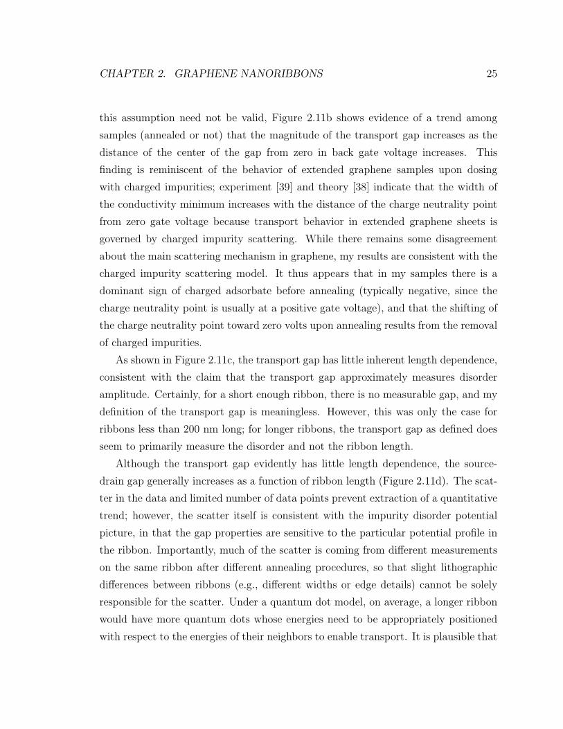
Figure 2.11: (a) Transport gap versus source-drain gap for all device sets (see Table2.1). No clear relationship can be extracted between the source-drain and transportgaps, suggesting that the two are independent quantities. (b) Transport gap sizeversus distance from zero. As the transport gap increases, its distance from zero alsotypically increases, implying that the transport gap is a measure of sample dopingby charged impurities. (c) Ribbon length versus transport gap; no connection isobserved between length and transport gap. Note that the three very disorderedoutliers from data set C1 revert to more common transport gap sizes upon annealing.(d) Ribbon length versus source-drain gap for all device sets. The source-drain gapgenerally grows with ribbon length, but there is a large amount of scatter, much ofit resulting from different measurements of the same sample after different annealingiterations. The 1σ error bars are derived from the linear fits defining the extent ofthe transport gaps, and from the uncertainty of the mean in the smoothing procedureused to calculate the source-drain gap.
CHAPTER 2. GRAPHENE NANORIBBONS 25
this assumption need not be valid, Figure 2.11b shows evidence of a trend among
samples (annealed or not) that the magnitude of the transport gap increases as the
distance of the center of the gap from zero in back gate voltage increases. This
finding is reminiscent of the behavior of extended graphene samples upon dosing
with charged impurities; experiment [39] and theory [38] indicate that the width of
the conductivity minimum increases with the distance of the charge neutrality point
from zero gate voltage because transport behavior in extended graphene sheets is
governed by charged impurity scattering. While there remains some disagreement
about the main scattering mechanism in graphene, my results are consistent with the
charged impurity scattering model. It thus appears that in my samples there is a
dominant sign of charged adsorbate before annealing (typically negative, since the
charge neutrality point is usually at a positive gate voltage), and that the shifting of
the charge neutrality point toward zero volts upon annealing results from the removal
of charged impurities.
As shown in Figure 2.11c, the transport gap has little inherent length dependence,
consistent with the claim that the transport gap approximately measures disorder
amplitude. Certainly, for a short enough ribbon, there is no measurable gap, and my
definition of the transport gap is meaningless. However, this was only the case for
ribbons less than 200 nm long; for longer ribbons, the transport gap as defined does
seem to primarily measure the disorder and not the ribbon length.
Although the transport gap evidently has little length dependence, the source-
drain gap generally increases as a function of ribbon length (Figure 2.11d). The scat-
ter in the data and limited number of data points prevent extraction of a quantitative
trend; however, the scatter itself is consistent with the impurity disorder potential
picture, in that the gap properties are sensitive to the particular potential profile in
the ribbon. Importantly, much of the scatter is coming from different measurements
on the same ribbon after different annealing procedures, so that slight lithographic
differences between ribbons (e.g., different widths or edge details) cannot be solely
responsible for the scatter. Under a quantum dot model, on average, a longer ribbon
would have more quantum dots whose energies need to be appropriately positioned
with respect to the energies of their neighbors to enable transport. It is plausible that

CHAPTER 2. GRAPHENE NANORIBBONS 26
this would, on average, increase the bias voltage required to push electrons across the
ribbon (i.e., increase the source-drain gap), as the data indicate.
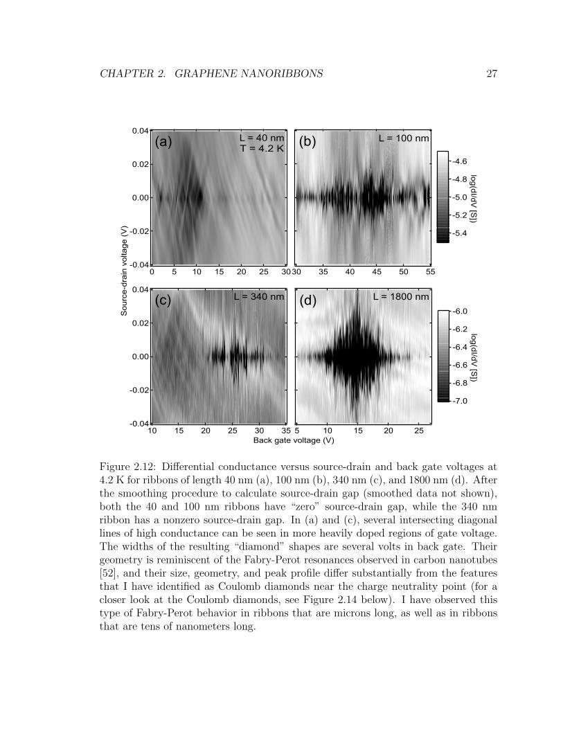
Another feature in Figure 2.11d is that the 30 and 40 nm-long ribbons had no
regions of back gate voltage where conductance was low enough to be considered
“gapped” per my definitions. On the other hand, ribbons that were at least 100 nm
long all had some gapped regions in gate voltage. Data illustrating the evolution
of the gap behavior for small ribbon lengths are shown in Figure 2.12. If transport
is controlled by puddles of localized carriers surrounded by regions of zero carrier
density, one would expect there to be some length below which a puddle is too well-
coupled to the leads to cause strong Coulomb blockade, resulting in no gap behavior.
Recent STM experiments indicate that charge puddles in extended graphene sheets
at the charge-neutrality point have an average length scale of about 20 nm [23].
Computational studies also suggest that the typical puddle size in graphene at the
charge-neutrality point is on the order of 10 nm [53]. Although it is not known how
this puddle size would be different in the case of nanoribbons, the largest ribbon
length below which there is no gap is on the order of tens of nanometers for these 30-
nm-wide ribbons; the length scales of the proposed quantum dots are thus consistent
with the results of the STM experiments and simulations.
2.6 Few-dot Coulomb blockade
Along with the above aggregate results in support of the charged-impurity-induced
quantum dot model, I have observed transport features in one particular ribbon that,
after annealing, strongly resemble Coulomb blockade through one main quantum dot
that may span much of the ribbon’s area. Figure 2.13 shows a plot of conductance
versus gate voltage from this sample. The left inset of Figure 2.13 shows a closeup of
a small range in back gate voltage from the same sweep; on this scale, very regular
conductance peaks can be identified. Hundreds of such peaks occur over a range of
more than 40 V in back gate with constant peak spacing. The peaks survive with
the same periodicity on the rising background in the more heavily doped region of
negative back gate voltage. As the back gate voltage is increased to about 15 V, the
CHAPTER 2. GRAPHENE NANORIBBONS 27
252015105
-7.0
-6.8
-6.6
-6.4
-6.2
-6.0
log(dI/dV [S
])
-0.04
-0.02
0.00
0.02
0.04
Sou
rce-
drai
n vo
ltage
(V)
353025201510Back gate voltage (V)
555045403530
-5.4
-5.2
-5.0
-4.8
-4.6
log(dI/dV [S
])
-0.04
-0.02
0.00
0.02
0.04
302520151050
L = 40 nmT = 4.2 K
L = 100 nm
L = 1800 nmL = 340 nm
(a) (b)
(d)(c)
Figure 2.12: Differential conductance versus source-drain and back gate voltages at4.2 K for ribbons of length 40 nm (a), 100 nm (b), 340 nm (c), and 1800 nm (d). Afterthe smoothing procedure to calculate source-drain gap (smoothed data not shown),both the 40 and 100 nm ribbons have “zero” source-drain gap, while the 340 nmribbon has a nonzero source-drain gap. In (a) and (c), several intersecting diagonallines of high conductance can be seen in more heavily doped regions of gate voltage.The widths of the resulting “diamond” shapes are several volts in back gate. Theirgeometry is reminiscent of the Fabry-Perot resonances observed in carbon nanotubes[52], and their size, geometry, and peak profile differ substantially from the featuresthat I have identified as Coulomb diamonds near the charge neutrality point (for acloser look at the Coulomb diamonds, see Figure 2.14 below). I have observed thistype of Fabry-Perot behavior in ribbons that are microns long, as well as in ribbonsthat are tens of nanometers long.

CHAPTER 2. GRAPHENE NANORIBBONS 28
0.35
0.30
0.25
0.20
0.15
0.10
0.05
0.00
Con
duct
ance
(2e2 /h
)
-50 -40 -30 -20 -10 0 10Back gate voltage (V)
0.05
0.04
0.03
0.02
0.01
0.00-21.2 -20.8 -20.4
0.10
0.08
0.06
0.04
0.02
0.007.26.86.4
Figure 2.13: Zero-bias conductance versus back gate voltage at 4.2 K of a 200-nm-long ribbon displaying highly periodic behavior after annealing. The individual peaksmaintain a constant peak spacing over much of the voltage range shown. Left inset:higher-resolution view of the conductance peaks between -21.5 V and -20 V. The peakspacing here is representative of the peak spacing for peaks in the back gate voltagerange -40 V to 5 V. Right inset: higher-resolution view of the conductance peaks formore positive back gate voltages; in this region, the peaks are far less regular thanthose shown in the left inset.

CHAPTER 2. GRAPHENE NANORIBBONS 29
peaks become less periodic. The right inset of Figure 2.13 shows a closeup of part of
the region in gate voltage where the behavior loses periodicity; while clusters of peaks
can have the same peak spacing, there are a number of peaks at irregular positions.
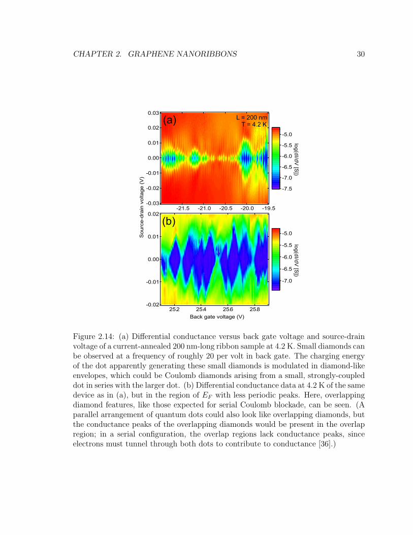
In plots of differential conductance versus bias and back gate voltage in the pe-
riodic region, as in Figure 2.14a, features that resemble the Coulomb diamonds of a
single quantum dot are apparent. The heights of these diamonds are modulated as
a function of gate voltage such that adjacent diamonds form diamond-like packets,
suggesting the presence of another physically smaller quantum dot that is strongly
coupled to a lead and is acting in series with the larger quantum dot responsible
for the smaller diamonds. In contrast, Figure 2.14b shows the less periodic region,
in which we find “overlapping” diamond features characteristic of Coulomb blockade
effects in a serial arrangement of multiple weakly coupled quantum dots.
The transition from periodic to less periodic behavior as the Fermi level is moved
through the transport gap is suggestive of Coulomb blockade occuring due to potential
inhomogeneities. Figure 2.15a shows a cartoon representation of a potential profile,
composed of one large “well” with some weaker modulation inside the well, which
could give rise to the observed phenomena. For some range of EF that includes the
EF shown in Figure 2.15a, there is only one isolated puddle, which spans most of the
ribbon. There is also a smaller puddle that is strongly coupled to one lead. But when
EF is in the range of the weaker modulation inside the well (Figure 2.15b) the ribbon
splits up into more than one isolated puddle; this is a serial arrangement of multiple
weakly tunnel-coupled quantum dots.
It is possible that the larger, more isolated quantum dot that exists in the periodic
region of gate voltage does not span as much of the ribbon as suggested by Figure
2.15a. However, if the dot takes up only a fraction of the ribbon, the potential
must be exceptionally smooth; any roughness will create other isolated quantum dots
near where the disorder potential energy crosses the Fermi level. Since this system
apparently only has one isolated dot, and since an extremely smooth disorder potential
seems unlikely, the isolated quantum dot probably does span most of the ribbon.
To quantitatively estimate the dot size, one can use the peak spacing (∼ 0.05 V)
along with the capacitance per unit length calculated by Lin et al. [54] (∼ 3.5 ×
CHAPTER 2. GRAPHENE NANORIBBONS 30
-0.03
-0.02
-0.01
0.00
0.01
0.02
0.03
Sou
rce-
drai
n vo
ltage
(V)
-21.5 -21.0 -20.5 -20.0 -19.5
-7.5
-7.0
-6.5
-6.0
-5.5
-5.0
log(dI/dV [S
])
-0.02
-0.01
0.00
0.01
0.02
25.825.625.425.2Back gate voltage (V)
-7.0
-6.5
-6.0
-5.5
-5.0
log(dI/dV [S
])T = 4.2 K
L = 200 nm(a)
(b)
Figure 2.14: (a) Differential conductance versus back gate voltage and source-drainvoltage of a current-annealed 200 nm-long ribbon sample at 4.2 K. Small diamonds canbe observed at a frequency of roughly 20 per volt in back gate. The charging energyof the dot apparently generating these small diamonds is modulated in diamond-likeenvelopes, which could be Coulomb diamonds arising from a small, strongly-coupleddot in series with the larger dot. (b) Differential conductance data at 4.2 K of the samedevice as in (a), but in the region of EF with less periodic peaks. Here, overlappingdiamond features, like those expected for serial Coulomb blockade, can be seen. (Aparallel arrangement of quantum dots could also look like overlapping diamonds, butthe conductance peaks of the overlapping diamonds would be present in the overlapregion; in a serial configuration, the overlap regions lack conductance peaks, sinceelectrons must tunnel through both dots to contribute to conductance [36].)

CHAPTER 2. GRAPHENE NANORIBBONS 31
Energy(b)
(a)
Well-coupled dot Large, isolated dot
Small, isolated dots
Position
Position
Energy
EF
EF
Figure 2.15: Cartoon of a potential profile (energy versus position along the ribbon)that could give rise to the behavior observed in this 200-nm-long sample. (a) TheFermi level is set low enough such that there is one isolated dot that spans most of theribbon, as well as another dot that is well-coupled to one lead. This dot configurationcould lead to the slowly modulated but otherwise highly periodic Coulomb oscillationsshown in the left inset of Figure 2.13. As the Fermi level is raised, the sizes andcouplings of the dots change slightly, but this double-dot system persists essentiallyunaltered for a range of Fermi levels. (b) Once the Fermi level is high enough, theribbon splits up into several small, isolated quantum dots in series. One expects thissystem to exhibit aperiodic oscillations like those shown in the right inset of 2.13.
CHAPTER 2. GRAPHENE NANORIBBONS 32
10−20 F/nm) for a graphene nanoribbon of 30 nm width above 300 nm of SiO2. This
results in a dot area of 3000 nm2, which corresponds to a 100 nm-long dot if the dot
spans the width of the ribbon. This agrees with the qualitative argument above that
the main dot covers most of the ribbon.
The dot in this ribbon is probably not nucleated by a single impurity. Based on the
mobilities of extended graphene flakes measured outside the ribbon body, following
earlier models [39] the density of charged impurites near the graphene should be
roughly ∼ 2× 1013 cm−2 before annealing. Studies [55] on extended graphene flakes
have suggested that the maximum achievable mobilities for graphene on SiO2 are
limited to about 15,000 cm2V−1s−1, corresponding to an impurity density of roughly
1011 cm−2. Even if this maximum mobility could be achieved after several annealing
attempts, one would still expect more than one impurity within the area of this
ribbon. Since clustering of impurities and overscreening effects are likely, there need
not be a one to one correspondence between impurities and charge puddles.
Importantly, the gradual transition from periodic to aperiodic behavior observed in
Figures 2.13 and 2.14 suggests that the less periodic peaks are also Coulomb blockade
peaks. These conductance peaks in the less periodic region are similar in width and
lineshape to those in my other ribbons as well as to those in ribbons produced by
different processes [32, 1, 33, 56]. Given this point, Coulomb blockade phenomena are
likely being observed in other ribbon samples as well. While it has been proposed that
Anderson localization can create conductance peaks and transport gap phenomena
[31, 44], peaks created by Anderson localization would not occur with highly periodic
spacing over a wide range of Fermi energies, as in Figure 2.13.
2.7 Conclusions
My data provide evidence in support of a model of nanoribbon behavior in which
charged impurities in the vicinity of the ribbon create a disorder potential that, cou-
pled with some small energy gap, breaks the ribbon up into isolated puddles of charge
carriers that act as quantum dots. Annealing studies on nanoribbons have demon-
strated that the source-drain and transport gaps are distinct quantities, as expected

CHAPTER 2. GRAPHENE NANORIBBONS 33
within the quantum dot model. The transport gap appears to reflect the doping of
the sample as well as its disorder amplitude, suggesting that the gap phenomena arise
in large part from disorder due to charged impurities. Furthermore, the source-drain
gap is apparently not a simple function of ribbon length and width, but instead seems
to depend sensitively on the potential profile in the nanoribbon; this result is under-
standable within the quantum dot framework since the dots’ sizes, positions, and
tunnel barriers are controlled by the precise potential profile, and the transport prop-
erties of a system of quantum dots depend heavily on these parameters. Nonetheless,
longer ribbons tend to have larger source-drain gaps, and very short ribbons exhibit no
gap behavior; these trends are understood within a quantum dot model, since there is
some smallest length required to fit a well-isolated quantum dot in the ribbon to block
transport, and since a longer ribbon will on average have more quantum dots that
electrons must tunnel across for conduction, increasing the source-drain gap. Finally,
I provided data from a 200 nm long ribbon displaying highly periodic modulations of
conductance versus gate voltage; these modulations are identified as Coulomb block-
ade oscillations based on their similarity to Coulomb oscillations in single-quantum
dot systems. This supports the idea that the conductance peaks commonly observed
in nanoribbons arise from Coulomb blockade rather than from Anderson localization
due to edge disorder.
A recent experiment [57] using a scanning gate microscope has demonstrated
that quantum dots in graphene nanostructures can be located in space with high
spatial resolution. Future work could apply this scanning gate technique to a long
nanoribbon to image the localized states in the ribbon before and after annealing. If
my interpretation of the data presented in this chapter is correct, the distribution of
localized states should rearrange itself with annealing.
The apparent importance of disorder in determining transport properties of graphene
nanoribbons produced by lithography raises questions about the feasibility of using
such ribbons as next-generation transistor technology. Of course, it is possible that
the influence of disorder due to charged impurities near the ribbon relative to the in-
fluence of atomic-scale disorder at the ribbon edges may differ in ribbons fabricated by
different techniques. This variation may occur in ribbons lithographically fabricated

CHAPTER 2. GRAPHENE NANORIBBONS 34
via differing masking techniques, or more radically, by new methods which have been
proposed for making nanoribbons with atomically ordered edges [58, 59]. However,
my results imply that unless the strength of disorder due to charged impurities near
the ribbon can also be reduced (for instance, by suspending [49] the nanoribbons), the
transport behavior of these clean-edged nanoribbons will still be dominated by the
Coulomb blockade of multiple quantum dots. But perhaps, by carefully controlling
the amount of disorder in these ribbons, Coulomb blockade effects could be harnessed
to create reliable switching behavior.

Chapter 3
Topological insulators
3.1 Background
I mentioned in the previous chapter that the low-energy band structure of graphene
derived from basic tight-binding calculations consists of gapless Dirac cones. However,
these calculations neglect spin-orbit terms, which are expected to be small but nonzero
in graphene. A theoretical study by Kane and Mele reported in 2005 that when spin-
orbit terms are included in the calculation, small band gaps open at the Dirac points,
and traversing these band gaps are gapless, linearly-dispersing edge states (see Figure
3.1). The edge states are “helical”: states propagating in one direction are spin up,
and states propagating in the other direction are spin down [8].
Notably, because the Hamiltonian respects time-reversal symmetry, the crossing
of the edge states at kx = π/a is protected from any time-reversal-symmetric pertur-
bation. This follows from Kramers’ theorem in quantum mechanics, which states that
the energy levels of a time-reversal-invariant Hamiltonian must be degenerate. Under
time reversal, a momentum state | k〉 goes to | −k〉, but | kx = π/a〉 is equivalent
to its time-reversed partner because it is at the edge of the 1D Brillouin zone. The
point kx = π/a is called a “time-reversal-invariant point,” at which | kx〉 |↑〉 and its
time-reversed state | kx〉 |↓〉, guaranteed to be distinct states by Kramers’ theorem,
are degenerate. This forces the edge state bands in Figure 3.1 to meet at kx = π/a.
The time-reversal symmetry of the Hamiltonian requires that E(kx) = E(−kx),
35

CHAPTER 3. TOPOLOGICAL INSULATORS 36
Figure 3.1: The band structure of zigzag-edged graphene with the spin-orbit interac-tion. The gapless, linearly dispersing states are the quantum spin Hall edge states,which traverse the bulk energy gap. Taken from Kane and Mele [8].
or equivalently that E(π/a + q) = E(π/a − q) in Figure 3.1. Because edge states
with momenta −kx and kx have opposite spins, there are no states available for
elastic backscattering without a spin flip. Remarkably, therefore, localization of the
edge states cannot be induced by a random potential. Furthermore, Kane and Mele
showed that inelastic backscattering from weak electron-electron interactions is small
at low temperature. In total, the metallic nature of the edge states is extremely
robust to disorder [8].
This type of insulator described by Kane and Mele, which is an insulator in the
bulk but has gapless edge states protected by time-reversal symmetry traversing the
gap, is called a “quantum spin Hall” (QSH) insulator. A QSH insulator is topolog-
ically distinct from a trivial insulator, such as glass: a trivial insulator will always
have an even number of Kramers pair edge states for a given edge at a given energy,
while this number is always odd for a QSH insulator [9]. (The typical trivial insulator
has no edge states and thus zero Kramers pair edge states, but some trivial insulators
such as InAs do have states at their boundaries [60, 61].)
This topological distinction can be understood by referring to the hypothetical
band structures shown in Figure 3.2. At the time-reversal-invariant points Λa and
Λb, Kramers’ theorem requires double degeneracy, between spin up and spin down.
But for general k, the spin-orbit coupling splits this degeneracy into multiple bands.
CHAPTER 3. TOPOLOGICAL INSULATORS 37
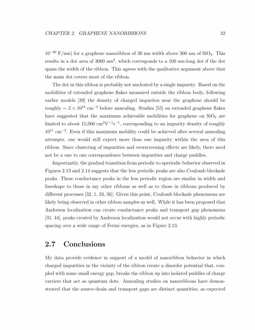
Figure 3.2: Bulk (shaded gray) and edge (solid black) bands for a QSH insulator (a)and a trivial insulator (b). Λa = 0 and Λb are time-reversal-invariant points. Bandsfor Λa < k < Λb and −Λb < k < Λa are mirror images due to time-reversal symmetry.There is always an odd number of edge states at a given energy for a QSH insulator,and an even number for a trivial insulator. Without breaking Kramers pairs at Λa
and Λb, it is not possible to deform the edge states in (a) such that a gap is openedin the edge states. However, it is possible to deform the edge states in (b) to producemetallic behavior at any point in the bulk gap. Taken from Fu, Kane, and Mele [12].
If the edge bands are split with the topology shown in Figure 3.2a, where the bulk
conduction and valence bands are linked with a single strand of edge states in E-k
space, it is impossible to deform the bands to create an insulator in the bulk gap
without breaking the degeneracy at Λa or Λb; this is the QSH insulator. By smoothly
deforming these edge bands, there can be more than one edge band crossing a given
energy, but the number of edge band crossings must remain odd: a band pulled down
through energy ε must come back up through ε since its energies at Λa and Λb are
fixed. On the other hand, if the edge bands have the topology of Figure 3.2b, it is
possible to smoothly deform the bands from the gapped structure shown to a metallic
band structure with edge states throughout the bulk gap; this is the trivial insulator.
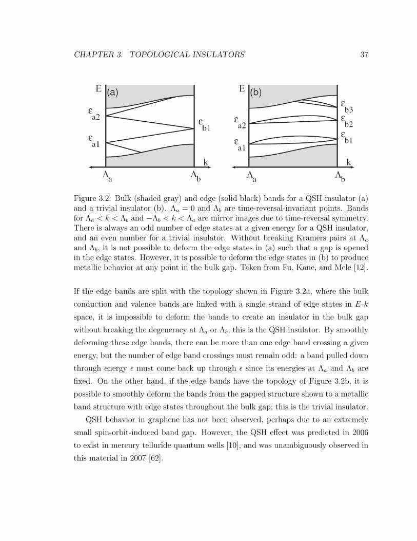
QSH behavior in graphene has not been observed, perhaps due to an extremely
small spin-orbit-induced band gap. However, the QSH effect was predicted in 2006
to exist in mercury telluride quantum wells [10], and was unambiguously observed in
this material in 2007 [62].

CHAPTER 3. TOPOLOGICAL INSULATORS 38
The QSH insulator in two dimensions has a natural generalization to three di-
mensions in materials known as “topological insulators.” A topological insulator is a
three-dimensional crystal with a time-reversal-invariant Hamiltonian and a band gap
for bulk states, but with states on the surface. Topological insulators can be either
“weak” (with topological invariant ν0 = 0) or “strong” (ν0 = 1). For ν0 = 0, the
surface Fermi arc always encloses an even number of time-reversal-invariant points,
which must be degenerate because of Kramers’ theorem. For ν0 = 1, the surface
Fermi arc encloses an odd number of time-reversal-invariant points. It can be shown
that a ν0 = 0 band structure can be deformed into a trivial insulator, and that a
ν0 = 1 band structure cannot. A strong topological insulator is thus topologically
distinct from a trivial insulator in the same sense that a QSH insulator is distinct
from a trivial insulator [11, 12].
Similarly to the 1D QSH case, at a given energy, if there is a surface state for k
there will be another for −k with the opposite spin. This results in a π Berry’s phase,
as the electron spin rotates by 2π when completing one Fermi arc. It has been further
shown that strong localization (Anderson localization) is not possible for the surface
states of a strong topological insulator, even in the presence of strong disorder such
as lattice defects [42, 43].
Several materials have been predicted to be strong topological insulators. Angle-
resolved photoemission spectroscopy (ARPES) experiments in 2008 [13] established
that Bi1−xSbx, predicted to be a topological insulator [22], indeed had Dirac-like
gapless surface states; spin-resolved ARPES measurements also verified the π Berry’s
phase [14]. Theoretical work published in 2009 [23] predicted that Bi2Se3, Bi2Te3, and
Sb2Te3 would be topological insulators; the predicted band structures were confirmed
by ARPES and scanning tunneling microscopy (STM) experiments [15, 16, 17, 18,
19, 20, 21].
A number of new physical effects are predicted for topological insulators. The
topological magnetoelectric effect, in which an applied electric field induces parallel
magnetization with a constant of proportionality quantized in odd multiples of the
fine structure constant, should be experimentally verifiable [63]. Majorana fermions,
exotic excitations which have not yet been experimentally observed, are predicted to
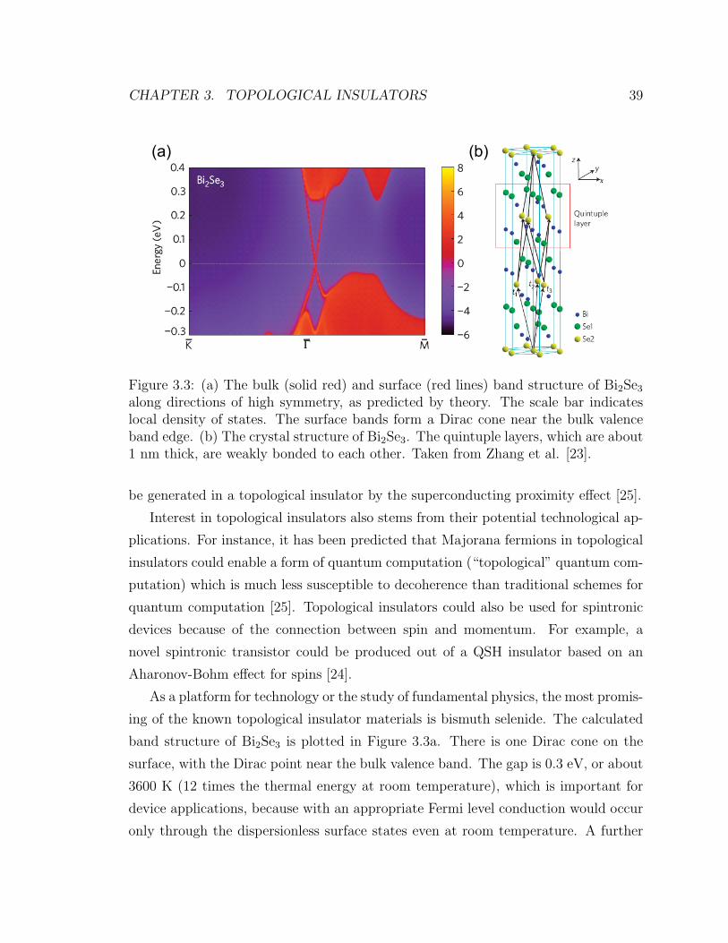
CHAPTER 3. TOPOLOGICAL INSULATORS 39
(a) (b)
Figure 3.3: (a) The bulk (solid red) and surface (red lines) band structure of Bi2Se3
along directions of high symmetry, as predicted by theory. The scale bar indicateslocal density of states. The surface bands form a Dirac cone near the bulk valenceband edge. (b) The crystal structure of Bi2Se3. The quintuple layers, which are about1 nm thick, are weakly bonded to each other. Taken from Zhang et al. [23].
be generated in a topological insulator by the superconducting proximity effect [25].
Interest in topological insulators also stems from their potential technological ap-
plications. For instance, it has been predicted that Majorana fermions in topological
insulators could enable a form of quantum computation (“topological” quantum com-
putation) which is much less susceptible to decoherence than traditional schemes for
quantum computation [25]. Topological insulators could also be used for spintronic
devices because of the connection between spin and momentum. For example, a
novel spintronic transistor could be produced out of a QSH insulator based on an
Aharonov-Bohm effect for spins [24].
As a platform for technology or the study of fundamental physics, the most promis-
ing of the known topological insulator materials is bismuth selenide. The calculated
band structure of Bi2Se3 is plotted in Figure 3.3a. There is one Dirac cone on the
surface, with the Dirac point near the bulk valence band. The gap is 0.3 eV, or about
3600 K (12 times the thermal energy at room temperature), which is important for
device applications, because with an appropriate Fermi level conduction would occur
only through the dispersionless surface states even at room temperature. A further

CHAPTER 3. TOPOLOGICAL INSULATORS 40
advantage of Bi2Se3 for any experimental purposes is that its surface band structure
is very simple (just one Dirac cone), which should facilitate the interpretation of data
and the planning of experiments.
3.2 Overview of experiment
To date, the main experimental probes of topological insulators have been ARPES
and STM, which give excellent information about the band structure of the material
in an ultra-clean environment. However, a number of interesting experiments, such as
those to probe Majorana fermions with the superconducting proximity effect, could
be most easily done as transport measurements. A transport experiment on a thin
film of bismuth selenide would allow for dynamic tunability of the Fermi level by an
electrostatic gate (a thin film is required in order to reduce the contribution of bulk
carriers to the two-dimensional carrier density, allowing for gate control). Performing
such transport measurements is also an important step toward making new topological
insulator technology, since devices would likely be made of thin topological insulator
films.
The immediate goal of my experiment was to produce thin films of bismuth se-
lenide which could be gated to move the Fermi level out of the bulk bands and across
the surface Dirac point. Thin films of bismuth selenide were to be produced from
bulk crystals and deposited onto insulating substrates by the same method used for
producing graphene; bismuth selenide was expected to cleave well into thin layers via
the graphene method because the bulk crystals are formed of weakly-bonded planes
(see Figure 3.3b).
I quickly found that thin films of this material, with thickness as small as 4 nm,
could in fact be produced and identified in an optical microscope by peeling the
bulk crystals and depositing them on the same SiO2 substrates used for graphene.
The focus of my work over the past year, done in collaboration with others in the
Goldhaber-Gordon lab (see Preface for details on the division of labor), has been on
characterizing and controlling the sample doping. It turns out to be very difficult to
control sample doping: not only are samples typically heavily n-doped, but the flakes

CHAPTER 3. TOPOLOGICAL INSULATORS 41
also may be doped differently on top and bottom surfaces.
As of this writing, we have made samples that can be gated across a peak in
resistance, which may correspond to the Fermi level crossing the Dirac point of one
or both surfaces of our samples. This peak in resistance occurs near the breakdown
region of the gate oxides, so it has not been possible to access much of the other side
of this resistance peak. Very recently, pre-prints of two experimental papers have
appeared with data similar to ours from samples prepared via the same mechanical
exfoliation technique [64, 65]. However, in contrast to the samples discussed in these
papers, our samples show a substantially larger resistivity change, suggesting that we
have achieved smaller bulk carrier densities.
The following will detail my work toward making gate-responsive bismuth selenide
devices. The transport measurement techniques used are similar to those used for
the graphene nanoribbon project (see Section 2.4), with the exception that some
measurements presented were taken at around 260 mK, the base temperature of the
helium-3 cryostat.
3.3 Sample fabrication
Samples were fabricated by mechanical exfoliation of Bi2Se3. First, a macroscopic
crystal, produced in Ian Fisher’s group at Stanford by slow cooling of melted bismuth,
selenide, and dopant elements, is placed on a piece of tape and repeatedly peeled to
leave a thin coating of Bi2Se3 crystals on the tape. The tape is then pressed down
onto a heavily n-doped silicon chip covered with 300 nm of thermal SiO2. The tape
is peeled off, leaving bismuth selenide flakes with thicknesses between 4 and 200 nm
on the SiO2.
As for graphene, thinner flakes can be identified by their different color in an
optical microscope, as shown in Figure 3.4. An AFM image of the flake in this
photograph, whose surface has some defects but is generally flat, is also shown in
Figure 3.4. Although this flake has some extent in both lateral directions, typically
the thinnest flakes have the aspect ratio of a ribbon: most are a few microns long and
only a few hundred nanometers wide.
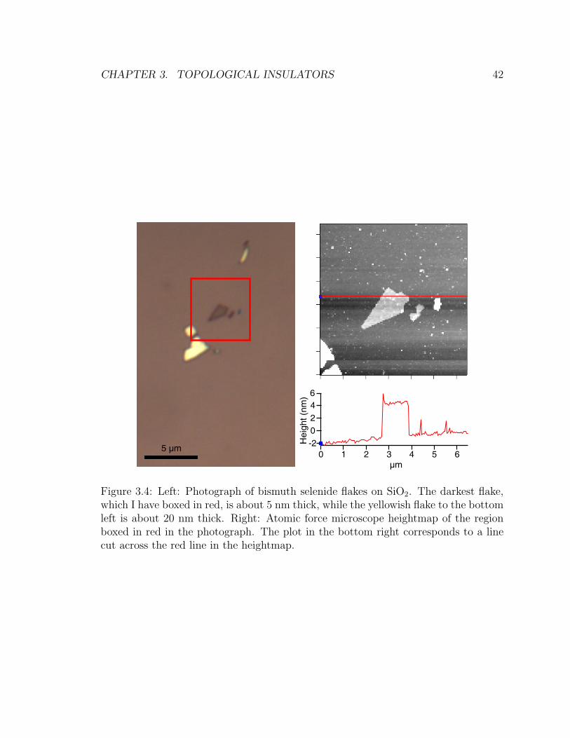
CHAPTER 3. TOPOLOGICAL INSULATORS 42
6420-2
6543210µm
Hei
ght (
nm)
5 µm
Figure 3.4: Left: Photograph of bismuth selenide flakes on SiO2. The darkest flake,which I have boxed in red, is about 5 nm thick, while the yellowish flake to the bottomleft is about 20 nm thick. Right: Atomic force microscope heightmap of the regionboxed in red in the photograph. The plot in the bottom right corresponds to a linecut across the red line in the heightmap.

CHAPTER 3. TOPOLOGICAL INSULATORS 43
5 µm
Figure 3.5: Photograph of a Hall bar device made of a flake approximately 60 nmthick.
Once flakes are found, they are contacted with titanium/gold contacts deposited
by electron-beam lithography as described in Section 2.3. The only difference from
the graphene fabrication is that before evaporating metal onto the bismuth selenide,
the chip is exposed to a UV-ozone clean for 3 minutes to remove residues and reduce
contact resistance. We found that the contact metal often had to be at least three
times thicker than the flake being contacted, or else some contacts would not work.
An example of a finished device is shown in Figure 3.5.
3.4 Carrier density measurements
Our earliest samples were made out of thicker flakes whose lateral dimensions were
on the order of microns. This allowed us to easily pattern either four contacts in
a van der Pauw geometry (contacts at four corners of a roughly square sample) or
six contacts in a Hall bar geometry like that in Figure 3.5; both of these geometries
permit measurement of longitudinal (Rxx) and transverse (Rxy) resistance, and thus
an estimation of the carrier density. The heavily n-doped silicon substrate acted as
a back gate. Samples that were at least 40 nm thick exhibited very low resistance
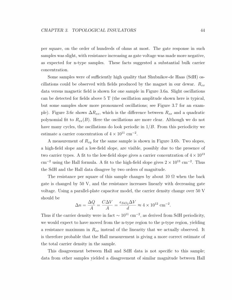
CHAPTER 3. TOPOLOGICAL INSULATORS 44
per square, on the order of hundreds of ohms at most. The gate response in such
samples was slight, with resistance increasing as gate voltage was made more negative,
as expected for n-type samples. These facts suggested a substantial bulk carrier
concentration.
Some samples were of sufficiently high quality that Shubnikov-de Haas (SdH) os-
cillations could be observed with fields produced by the magnet in our dewar. Rxx
data versus magnetic field is shown for one sample in Figure 3.6a. Slight oscillations
can be detected for fields above 5 T (the oscillation amplitude shown here is typical,
but some samples show more pronounced oscillations; see Figure 3.7 for an exam-
ple). Figure 3.6c shows ∆Rxx, which is the difference between Rxx and a quadratic
polynomial fit to Rxx(B). Here the oscillations are more clear. Although we do not
have many cycles, the oscillations do look periodic in 1/B. From this periodicity we
estimate a carrier concentration of 4× 1011 cm−2.
A measurement of Rxy for the same sample is shown in Figure 3.6b. Two slopes,
a high-field slope and a low-field slope, are visible, possibly due to the presence of
two carrier types. A fit to the low-field slope gives a carrier concentration of 4× 10¹³
cm−2 using the Hall formula. A fit to the high-field slope gives 2× 1013 cm−2. Thus
the SdH and the Hall data disagree by two orders of magnitude.
The resistance per square of this sample changes by about 10 Ω when the back
gate is changed by 50 V, and the resistance increases linearly with decreasing gate
voltage. Using a parallel-plate capacitor model, the carrier density change over 50 V
should be
∆n =∆Q
A=C∆V
A=εSiO2∆V
d≈ 4× 1012 cm−2.
Thus if the carrier density were in fact ∼ 1011 cm−2, as derived from SdH periodicity,
we would expect to have moved from the n-type region to the p-type region, yielding
a resistance maximum in Rxx instead of the linearity that we actually observed. It
is therefore probable that the Hall measurement is giving a more correct estimate of
the total carrier density in the sample.
This disagreement between Hall and SdH data is not specific to this sample;
data from other samples yielded a disagreement of similar magnitude between Hall
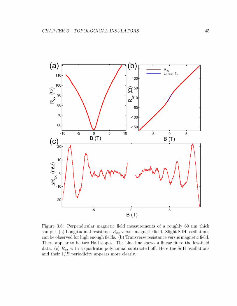
CHAPTER 3. TOPOLOGICAL INSULATORS 45
110
100
90
80
70
60
xx
-10 -5 0 5 10B (T)
-150
-100
-50
0
50
100
xy-5 0 5
B (T)
R Linear fit
-20
-10
0
10
20
∆Rxx
-5 0 5B (T)
RR(Ω
)
(Ω)
(mΩ
)
xy(a)
(c)
(b)
Figure 3.6: Perpendicular magnetic field measurements of a roughly 60 nm thicksample. (a) Longitudinal resistance Rxx versus magnetic field. Slight SdH oscillationscan be observed for high enough fields. (b) Transverse resistance versus magnetic field.There appear to be two Hall slopes. The blue line shows a linear fit to the low-fielddata. (c) Rxx with a quadratic polynomial subtracted off. Here the SdH oscillationsand their 1/B periodicity appears more clearly.

CHAPTER 3. TOPOLOGICAL INSULATORS 46
and SdH carrier density estimates. A plausible explanation for the disagreement
between Hall and SdH is that surface states are creating the SdH oscillations while
bulk carriers dominate the Hall signal. However, there is no direct evidence to support
this explanation.
One sample did show what appeared to be at least two SdH frequencies. These
data are shown in Figure 3.7. Assuming two frequencies, and examining peaks in
the high-field region, we extract carrier densities ∼ 1012 cm−2 for both carrier types.
However, with the limited number of oscillations available, it is far from clear that
there are only two frequencies; data at higher fields would give a clearer picture. In
contrast, Rxy yields a density of 4× 1013 cm−2 (as in Figure 3.6, there are two slopes
in Rxy, but both give about the same density).
The presence of multiple SdH frequencies supports the theory that there are car-
riers in different bands with different mobilities, and that SdH is only probing certain
types of carriers. This would explain the disagreement with Hall data. However, it
remains unclear whether or not any of these SdH oscillations are due to surface states
(“topological” or otherwise). To help answer this question it would be fruitful to
measure the dependence of the SdH oscillations on the angle between the magnetic
field and the plane of the Bi2Se3 flake, and to measure SdH at higher fields.
Oddly, samples produced from crystals grown with different dopant levels, includ-
ing those that were p-doped as bulk crystals, had n-type densities extracted from
Hall data of about 1013 cm−2. While a sufficiently high initial dopant concentra-
tion would likely induce p-type behavior, crystal purity would be low and scattering
would increase. A more desirable solution, which will be the focus of future work, is
to determine and reduce the source of the n-doping in our thin film samples.
3.5 Resistance peak in top-gated samples
In order to gain more tunability than we had with the thicker flakes discussed in
the previous section, we produced top-gated samples on thinner flakes (5 to 15 nm
thick). Because these thinner flakes were usually long and narrow, most did not have
space to deposit extra terminals for Hall measurements. A typical top-gated device

CHAPTER 3. TOPOLOGICAL INSULATORS 47
0.17
0.15
0.13
0.11321
-100
0
100
-5 0 5
11
10
9
8
86420
-0.3
-0.2
-0.1
0.0
0.1
0.2
0.3R
xy(Ω
)
R(Ω
)xx
∆R(Ω
)xx
B (T)
1/B
(1/T
)
B (T)
Peak index
Figure 3.7: Four-terminal resistance versus perpendicular magnetic field for a 60 nmthick sample at 260 mK. Rxx is shown in red, and ∆Rxx, which is Rxx minus apolynomial fit, is shown in blue. It appears that there are at least two SdH periods.The upper left inset shows peak positions for peaks in the regime B > 6 T. Transverseresistance versus magnetic field is shown in the lower inset.

CHAPTER 3. TOPOLOGICAL INSULATORS 48
5 µm
V-
V+I+
I-
TG
Figure 3.8: Photograph of a top-gated device. Current flows between leads I+ andI-, and the top gate (TG) tunes EF in the region between V+ and V-, across which avoltage drop is measured to calculate resistance. The Bi2Se3 flake is long and narrow,and has been false-colored red.
is shown in Figure 3.8. After the flake was deposited on the SiO2 and contacts were
patterned, the chip was coated in 30-50 nm of alumina by atomic layer deposition
to form a dielectric for the top gate. A final step of lithography was performed to
pattern the top gate between the innermost contacts.
The high quality of the dielectric allows the application of over 1 V on the top
gate per nm of dielectric thickness before breakdown, and given the high dielectric
constant of alumina, the top gate allows for an order of magnitude larger density
change than does the back gate (∼ 6× 1013 cm−2 instead of ∼ 8× 1012 cm−2), which
can only withstand about 100 V. The combination of thinner samples and the top
gate thus gave us enough tunability to observe a peak in the resistance versus gate
voltage in over ten samples. Peaks from eight different samples are shown in Figure
3.9. Every sample that we made was heavily n-doped (even those from significantly p-
doped bulk crystals): the peak consistently occured at large negative voltages near the
oxide breakdown voltage. All had metallic temperature dependence. The resistivities
at peak for the various samples ranged from 1 to 20 kΩ per square, with no clear
dependence on lateral size or thickness of the sample.
Our highest peak resistivities are an order of magnitude larger than those in other
studies, which reported peak resistivities on the order of 2 kΩ [65] and 60 Ω [64]
per square (see Figure 3.10). Furthermore, in our samples, the fractional resistance
CHAPTER 3. TOPOLOGICAL INSULATORS 49
30 25 20 15 10 5 0
1.29
1.31
1.33
1.35
1.37
50 40 30 20 10 02.5
3
3.5
4
4.5
30 25 20 15 10 5 00
4
8
12
16
20
35 30 25 20 15 10 5 010
15
20
25
30
35
50 40 30 20 10 04.5
5
5.5
6
6.5
7
50 40 30 20 10 0
4
6
8
10
12
14
30 25 20 15 10 5 0
8
9
10
11
100 50 0 50
10
14
18
22
Top gate voltage (V)
R (k
Ω)
R (k
Ω)
Top gate voltage (V) Back gate voltage (V)
VBG = -100 V900 x 330 x 15
1200 x 350 x 12
VBG = -50 V450 x 500 x 10
VBG = -120 V2400 x 275 x 5
VBG = -110 V2300 x 360 x 15
VBG = -100 V2300 x 1750 x 7
VBG = -100 V800 x 375 x 15
VBG = -100 V950 x 300 x 5
(a) (b) (c)
(d) (e) (f)
(g) (h)
Figure 3.9: Resistance versus gate voltage at 4 K for eight samples. Plot (h) showsa peak observed with just a back gate. Device dimensions are written in the format(length in nm) × (width in nm) × (thickness in nm), where the length is measuredbetween the V+ and V- contacts (see Figure 3.8). The back gate voltage VBG washeld at a constant value, specified on the plots, during the top gate sweeps. All datawere taken in a 4-terminal geometry except for (c) and (h), which were 2-terminalmeasurements. The 2-terminal geometry should add less than 2 kΩ (mainly dueto resistive electrical filters in the cryostat) to the total resistance. The switchingbehavior in plot (g) resulted from NO2 exposure, as discussed in Section 3.7.

CHAPTER 3. TOPOLOGICAL INSULATORS 50
(a) (b)
Figure 3.10: Resistance peaks from (a) Steinberg et al. [64] and (b) Checkelsky et al.[65], reproduced here (with slight modification) for comparison to our data in Figure3.9. These peaks are qualitatively similar to ours, but show lower resistance and lackthe same sort of sharper drop-off that we observe in some samples on the hole side ofthe peak. See text for discussion.
change between the saturated n-type region and the peak region is as high as that
reported by Checkelsky et al. [65] and substantially higher than the 2% change
reported by Steinberg et al. [64]. Bulk carriers provide a residual conductivity at the
resistance peak and decrease gate-tunability; thus, despite the significant n-doping
that we observe, the fact that we see the lowest residual conduction and a large
resistance modulation with gate voltage suggests that we have achieved some of the
lowest bulk carrier contributions to date in Bi2Se3 thin films.
Considering the predicted band structure of Bi2Se3 shown in Figure 3.3a, one does
expect resistance peaks such as those in Figure 3.9. When the Fermi level is in the
bulk gap, the resistance should look similar to that of graphene, which has a peak
when the Fermi level moves through the Dirac point [5]. The resistance should drop
off more sharply on the side of negative voltage (hole side) as the surface state Dirac
point is expected to be very near to the bulk valence band edge. We observe this
sharper drop-off in most but not all samples, as can be seen in Figure 3.9. Other
studies have generally not observed this drop-off, although one trace in Figure 3.10a
does show a sharp resistance drop at extreme negative voltages. In samples that do
not display a sharper drop-off on the hole side of the peak, it may be that the surface

CHAPTER 3. TOPOLOGICAL INSULATORS 51
is doped differently from the bulk, or that the gate oxide simply breaks down before
the drop-off is observed. Further work is needed to determine the exact significance
of these resistance peaks.
Because topological insulator surface states are protected by time-reversal symme-
try, one might expect that the application of a magnetic field to break time-reversal
symmetry would have a significant effect on the surface states. This was the case in
HgTe quantum wells: the application of a magnetic field opened a gap in the QSH
edge states [62]. Due to problems with hysteresis and oxide breakdown, we only
measured one sample near the resistance peak under a high magnetic field. The 9 T
and 0 T resistances versus gate voltage showed no qualitative differences and limited
quantitative differences which could have been the result of hysteresis. While these
data might indicate that the transport behavior of the surface states is unaffected by
a 9 T field, it might also indicate that the bulk carrier concentration is too high to
observe the behavior of the predicted surface states.
3.6 Weak antilocalization
We have identified weak antilocalization features in our samples, as is theoretically
expected for topological insulators due to the π Berry’s phase [22]. Figure 3.11 shows
plots of ∆G, which is the ensemble-averaged conductance with the quadratic back-
ground subtracted off, at three different temperatures (see figure caption for details).
The ensemble-averaging is done by averaging over 30 different back gate voltages,
which should suppress universal conductance fluctuation (UCF) features. The weak
antilocalization peak is clearly observed in ∆G, and grows larger with decreasing
temperature as expected. Furthermore, features away from the weak antilocalization
peak persist after ensemble-averaging and changing the temperature. These features
also get larger with decreasing temperature. It is not yet clear how to interpret these
features; they will be the subject of future study.

CHAPTER 3. TOPOLOGICAL INSULATORS 52
0.15
0.10
0.05
0.00
-2 -1 0 1 2
0.2
0.1
0
-2 0 1 2-1
∆G (e
/h)
2
B (T)
B (T)
G (e
/h)
2
4 K2 K261 mK
Figure 3.11: Two-terminal conductance behavior versus perpendicular magnetic fieldand temperature for a ribbon-type sample 10 nm thick. The main panel shows ∆Gat three different temperatures. ∆G is computed by first taking a trace of G(B) ata given back gate voltage and fitting a quadratic polynomial to a region away fromthe peak near B = 0, as shown in the inset. The polynomial is subtracted fromG(B), and the resulting function for 30 back gate voltages in 1 V steps between -15V and 15 V is averaged to give ∆G. This averaging procedure suppresses UCF. Theweak antilocalization peak can be clearly seen in ∆G, and gets larger with decreasingtemperature. Furthermore, there are features away from the weak antilocalizationpeak that are evident at all temperatures and get larger with decreasing temperature.

CHAPTER 3. TOPOLOGICAL INSULATORS 53
3.7 Controlling sample doping
Without being able to tune the Fermi level far past the resistance peak in the hole
direction, it is difficult to prove that the resistance peak corresponds to the Fermi level
crossing the surface Dirac point; perhaps there are other resistance peaks when more
electrons are removed from the film, which would suggest spatially inhomogeneous
doping. In order to try to bring the resistance peak closer to zero gate voltage, bismuth
selenide crystals with different dopants and several different dopant concentrations
were used to prepare thin films. However, all of the thin-film samples measured were
found to be heavily n-doped, even those made from bulk crystals measured to be
p-doped in bulk form.
This suggests that perhaps the samples are being doped as a byproduct of lithog-
raphy or the mechanical exfoliation (tape peeling) method. Because the thin film
samples have such a large surface to volume ratio, they are more susceptible than
bulk crystals to doping from resist and solvent residues or from water or other ad-
sorbates from the atmosphere. Furthermore, Bi2Se3 samples are prone to becoming
n-type due to the creation of selenium vacancies which act as electron donors [15];
heating the sample to 160C to bake the resist could be creating more vacancies.
However, samples produced with an 80C bake process were still heavily n-doped.
We attempted to counteract the doping by trapping NO2 under the alumina layer
that forms the top gate oxide [66], as ARPES experiments have found that NO2 dopes
the surface states of Bi2Se3 with holes [19]. Approximately 10 samples less than 15 nm
thick were exposed to NO2 before oxide growth. Several of these samples, especially
those with the largest NO2 exposure, had severe charge-rearrangement problems that
led to noisy measurements (see Figure 3.9g). Those without noise problems were still
as heavily n-doped as typical top-gated samples.
As an alternative approach to the doping problem, we tried to prevent the samples
from being doped by contaminants from lithography and the atmosphere by perform-
ing the bismuth selenide exfoliation and deposition on the SiO2 substrate in a glove
bag filled with nitrogen at positive pressure. Immediately after deposition and while
inside the glove bag, we spun on and a single layer of 950 molecular weight PMMA

CHAPTER 3. TOPOLOGICAL INSULATORS 54
1 0.8 0.6 0.4 0.2 05.8
5.9
6
6.1
6.2
6.3
6.4R
(kΩ
)
0.6 0.5 0.4 0.3 0.2 0.1 0
8.3
8.4
8.5
8.6
Top gate voltage (V)
Figure 3.12: Four-terminal resistance versus top gate voltage at zero back gate voltageand room temperature for two samples fabricated in a glove bag (see text). Thedata on the left is for a sample about 10 nm thick, and the data on the right isfor a sample about 15 nm thick. The resistance change between 0 and -1 volts issubstantially larger than in other samples at room temperature, and the thickness ofthe crosslinked PMMA dielectric is about the same as that of the alumina.
(2% in solvent) and baked it at 160C. The sample was removed from the glove bag
and a bismuth selenide flake was identified under the optical microscope. The PMMA
polymers over the flake were then crosslinked in the SEM by bombardment with a
high electron dose; this created a film of PMMA, estimated to be 30 nm thick, that
could not be removed by subsequent processing and hopefully protected the surface
of the sample from adsorbates. Contacts and a top gate were then patterned to the
sample.
Plots of resistance versus top gate voltage at room temperature are shown in
Figure 3.12 for the two samples produced so far by this method. The resistance
change with gate voltage near zero volts is unusually high in both samples: about
10% from 0 to -1 V, as compared with about 2% in alumina-coated samples. The
difference is likely not attributable to the different dielectrics, since the thicknesses
of the PMMA and alumina should be about the same, and we expect the dielectric
constant of the PMMA to be lower. This suggests that the PMMA samples may be
CHAPTER 3. TOPOLOGICAL INSULATORS 55
doped closer to the resistance peak and/or that the samples may be of high mobility.
One of these two PMMA samples failed while being cooled down to 4 K; the other
survived to be measured at 4 K, but the top gate broke down at -3 V after showing
very little gate response. The reasons for the low breakdown voltage and the modest
gate response are unknown. The back gate response also indicated very heavily n-
doped samples, with little resistance change and no clear resistance peak. However,
recent transport experiments on Bi2Se3 thin films [64] have found evidence that the
top gate primarily tunes the top surface, while the back gate primarily tunes the
bottom surface. Perhaps this is occuring in our crosslinked PMMA samples, which
would explain the high top gate response but low back gate response.
The method of producing samples in an inert atmosphere shows some promise,
and will be the subject of future work. PMMA may not be the best candidate material
for protecting the sample from atmospheric dopants, and the large dose required to
crosslink it may damage the crystal beneath the resist. We will attempt to use other
resists as well in future trials.
3.8 Conclusions
I have described progress toward producing gate-responsive thin films of Bi2Se3 by
mechanical exfoliation and electron-beam lithography. Devices produced so far have
demonstrated that a resistance peak can be reached at sufficiently large negative
voltage on the gates in sufficiently thin (less than 20 nm) samples. We have likely
obtained some of the lowest 2D concentrations of bulk carriers to date in bismuth
selenide thin films. However, all samples remain heavily n-doped, even those that
are exfoliated from p-type bulk crystals. It also may be the case that the surfaces
and bulk are at different Fermi levels, which complicates the interpretation of the
transport data. Near-term goals for this project include attempting to control sample
doping by producing samples in an inert environment and protecting them from
adsorbates. Longer-term goals include increasing sample quality to observe quantum
Hall behavior, and patterning superconducting leads to samples to measure signatures
of Majorana fermions.
Bibliography
[1] Todd, K., Chou, H.-T., Amasha, S., and Goldhaber-Gordon, D. Quantum Dot
Behavior in Graphene Nanoconstrictions. Nano Lett. 9, 416–421 (2009).
[2] Gallagher, P., Todd, K., and Goldhaber-Gordon, D. Disorder-induced gap be-
havior in graphene nanoribbons. Phys. Rev. B 81(11), 115409 (2010).
[3] Wallace, P. R. The band theory of graphite. Phys. Rev. 71(9), 622–634 (1947).
[4] Castro Neto, A. H., Guinea, F., Peres, N. M. R., Novoselov, K. S., and Geim,
A. K. The electronic properties of graphene. Rev. Mod. Phys. 81, 109–162 (2009).
[5] Novoselov, K. S., Geim, A. K., Morozov, S. V., Jiang, D., Zhang, Y., Dubonos,
S. V., Grigorieva, I. V., and Firsov, A. A. Electric Field Effect in Atomically
Thin Carbon Films. Science 306, 666–669 (2004).
[6] Lin, Y., Dimitrakopoulos, C., Jenkins, K. A., Farmer, D. B., Chiu, H., Grill,
A., and Avouris, P. 100-GHz Transistors from Wafer-Scale Epitaxial Graphene.
Science 327, 662– (2010).
[7] Han, M. Y., Ozyilmaz, B., Zhang, Y., and Kim, P. Energy Band-Gap Engineering
of Graphene Nanoribbons. Phys. Rev. Lett. 98(20), 206805 (2007).
[8] Kane, C. L. and Mele, E. J. Quantum Spin Hall Effect in Graphene. Phys. Rev.
Lett. 95(22), 226801 (2005).
[9] Kane, C. L. and Mele, E. J. Z2 Topological Order and the Quantum Spin Hall
Effect. Phys. Rev. Lett. 95(14), 146802 (2005).
56
BIBLIOGRAPHY 57
[10] Bernevig, B. A., Hughes, T. L., and Zhang, S. Quantum Spin Hall Effect and
Topological Phase Transition in HgTe Quantum Wells. Science 314, 1757 (2006).
[11] Moore, J. E. and Balents, L. Topological invariants of time-reversal-invariant
band structures. Phys. Rev. B 75(12), 121306 (2007).
[12] Fu, L., Kane, C. L., and Mele, E. J. Topological Insulators in Three Dimensions.
Phys. Rev. Lett. 98(10), 106803 (2007).
[13] Hsieh, D., Qian, D., Wray, L., Xia, Y., Hor, Y. S., Cava, R. J., and Hasan,
M. Z. A topological Dirac insulator in a quantum spin Hall phase. Nature 452,
970–974 (2008).
[14] Hsieh, D., Xia, Y., Wray, L., Qian, D., Pal, A., Dil, J. H., Osterwalder, J.,
Meier, F., Bihlmayer, G., Kane, C. L., Hor, Y. S., Cava, R. J., and Hasan,
M. Z. Observation of Unconventional Quantum Spin Textures in Topological
Insulators. Science 323, 919 (2009).
[15] Hor, Y. S., Richardella, A., Roushan, P., Xia, Y., Checkelsky, J. G., Yazdani,
A., Hasan, M. Z., Ong, N. P., and Cava, R. J. p -type Bi2Se3 for topological
insulator and low-temperature thermoelectric applications. Phys. Rev. B 79(19),
195208 (2009).
[16] Xia, Y., Qian, D., Hsieh, D., Wray, L., Pal, A., Lin, H., Bansil, A., Grauer, D.,
Hor, Y. S., Cava, R. J., and Hasan, M. Z. Observation of a large-gap topological-
insulator class with a single Dirac cone on the surface. Nat. Phys. 5, 398–402
(2009).
[17] Hsieh, D., Xia, Y., Qian, D., Wray, L., Dil, J. H., Meier, F., Osterwalder, J.,
Patthey, L., Checkelsky, J. G., Ong, N. P., Fedorov, A. V., Lin, H., Bansil, A.,
Grauer, D., Hor, Y. S., Cava, R. J., and Hasan, M. Z. A tunable topological
insulator in the spin helical Dirac transport regime. Nature 460, 1101–1105
(2009).

BIBLIOGRAPHY 58
[18] Chen, Y. L., Analytis, J. G., Chu, J., Liu, Z. K., Mo, S., Qi, X. L., Zhang, H. J.,
Lu, D. H., Dai, X., Fang, Z., Zhang, S. C., Fisher, I. R., Hussain, Z., and Shen, Z.
Experimental Realization of a Three-Dimensional Topological Insulator, Bi2Te3.
Science 325, 178 (2009).
[19] Xia, Y., Qian, D., Hsieh, D., Shankar, R., Lin, H., Bansil, A., Fedorov, A. V.,
Grauer, D., Hor, Y. S., Cava, R. J., and Hasan, M. Z. Topological Control:
Systematic control of topological insulator Dirac fermion density on the surface
of Bi2Te3. ArXiv e-prints 0907.3089 (2009).
[20] Alpichshev, Z., Analytis, J. G., Chu, J., Fisher, I. R., Chen, Y. L., Shen, Z. X.,
Fang, A., and Kapitulnik, A. STM Imaging of Electronic Waves on the Surface of
Bi2Te3: Topologically Protected Surface States and Hexagonal Warping Effects.
Phys. Rev. Lett. 104(1), 016401 (2010).
[21] Hsieh, D., Xia, Y., Qian, D., Wray, L., Meier, F., Dil, J. H., Osterwalder,
J., Patthey, L., Fedorov, A. V., Lin, H., Bansil, A., Grauer, D., Hor, Y. S.,
Cava, R. J., and Hasan, M. Z. Observation of Time-Reversal-Protected Single-
Dirac-Cone Topological-Insulator States in Bi2Te3 and Sb2Te3. Phys. Rev. Lett.
103(14), 146401 (2009).
[22] Fu, L. and Kane, C. L. Topological insulators with inversion symmetry. Phys.
Rev. B 76(4), 045302 (2007).
[23] Zhang, H., Liu, C., Qi, X., Dai, X., Fang, Z., and Zhang, S. Topological insulators
in Bi2Se3, Bi2Te3 and Sb2Te3 with a single Dirac cone on the surface. Nat. Phys.
5, 438–442 (2009).
[24] Maciejko, J., Kim, E., and Qi, X. Spin Aharonov-Bohm effect and topological
spin transistor. ArXiv e-prints 0908.0564 (2009).
[25] Fu, L. and Kane, C. L. Superconducting Proximity Effect and Majorana
Fermions at the Surface of a Topological Insulator. Phys. Rev. Lett. 100(9),
096407 (2008).

BIBLIOGRAPHY 59
[26] Geim, A. K. and Novoselov, K. S. The rise of graphene. Nat. Mater. 6, 183–191
(2007).
[27] Kravchenko, S. V. and Sarachik, M. P. Metal insulator transition in two-
dimensional electron systems. Rep. Prog. Phys. 67, 1–44 (2004).
[28] Brey, L. and Fertig, H. A. Electronic states of graphene nanoribbons studied
with the Dirac equation. Phys. Rev. B 73(23), 235411 (2006).
[29] Son, Y., Cohen, M. L., and Louie, S. G. Energy Gaps in Graphene Nanoribbons.
Phys. Rev. Lett. 97(21), 216803 (2006).
[30] Yang, L., Park, C.-H., Son, Y.-W., Cohen, M. L., and Louie, S. G. Quasiparticle
Energies and Band Gaps in Graphene Nanoribbons. Phys. Rev. Lett. 99(18),
186801 (2007).
[31] Evaldsson, M., Zozoulenko, I. V., Xu, H., and Heinzel, T. Edge-disorder-induced
Anderson localization and conduction gap in graphene nanoribbons. Phys. Rev.
B 78(16), 161407 (2008).
[32] Stampfer, C., Guttinger, J., Hellmuller, S., Molitor, F., Ensslin, K., and Ihn, T.
Energy Gaps in Etched Graphene Nanoribbons. Phys. Rev. Lett. 102(5), 056403
(2009).
[33] Liu, X., Oostinga, J. B., Morpurgo, A. F., and Vandersypen, L. M. K. Elec-
trostatic confinement of electrons in graphene nanoribbons. Phys. Rev. B 80,
121407(R) (2009).
[34] Molitor, F., Jacobsen, A., Stampfer, C., Guttinger, J., Ihn, T., and Ensslin, K.
Transport gap in side-gated graphene constrictions. Phys. Rev. B 79(7), 075426
(2009).
[35] Heinzel, T. Mesoscopic Electronics in Solid State Nanostructures, volume 2,
chapter 10. Wiley-VCH (2007).

BIBLIOGRAPHY 60
[36] van der Wiel, W. G., de Franceschi, S., Elzerman, J. M., Fujisawa, T., Tarucha,
S., and Kouwenhoven, L. P. Electron transport through double quantum dots.
Rev. of Mod. Phys. 75, 1–22 (2002).
[37] Sols, F., Guinea, F., and Neto, A. H. C. Coulomb Blockade in Graphene Nanorib-
bons. Phys. Rev. Lett. 99(16), 166803 (2007).
[38] Adam, S., Hwang, E. H., Galitski, V. M., and Das Sarma, S. A self-consistent
theory for graphene transport. PNAS 104, 18392–18397 (2007).
[39] Chen, J.-H., Jang, C., Adam, S., Fuhrer, M. S., Williams, E. D., and Ishigami,
M. Charged-impurity scattering in graphene. Nat. Phys. 4, 377–381 (2008).
[40] Katsnelson, M. I., Novoselov, K. S., and Geim, A. K. Chiral tunnelling and the
Klein paradox in graphene. Nat. Phys. 2, 620–625 (2006).
[41] Nomura, K. and MacDonald, A. H. Quantum Transport of Massless Dirac
Fermions. Phys. Rev. Lett. 98(7), 076602 (2007).
[42] Nomura, K., Koshino, M., and Ryu, S. Topological Delocalization of Two-
Dimensional Massless Dirac Fermions. Phys. Rev. Lett. 99(14), 146806 (2007).
[43] Bardarson, J. H., Tworzyd lo, J., Brouwer, P. W., and Beenakker, C. W. J.
One-Parameter Scaling at the Dirac point in graphene. Phys. Rev. Lett. 99(10),
106801 (2007).
[44] Mucciolo, E. R., Castro Neto, A. H., and Lewenkopf, C. H. Conductance quan-
tization and transport gaps in disordered graphene nanoribbons. Phys. Rev. B
79(7), 075407 (2009).
[45] Ferrari, A. C., Meyer, J. C., Scardaci, V., Casiraghi, C., Lazzeri, M., Mauri, F.,
Piscanec, S., Jiang, D., Novoselov, K. S., Roth, S., and Geim, A. K. Raman
Spectrum of Graphene and Graphene Layers. Phys. Rev. Lett. 97(18), 187401
(2006).

BIBLIOGRAPHY 61
[46] Chen, Z., Lin, Y.-M., Rooks, M. J., and Avouris, P. Graphene nano-ribbon
electronics. Physica E 40, 228–232 (2007).
[47] Elias, D. C., Nair, R. R., Mohiuddin, T. M. G., Morozov, S. V., Blake, P., Halsall,
M. P., Ferrari, A. C., Boukhvalov, D. W., Katsnelson, M. I., Geim, A. K., and
Novoselov, K. S. Control of Graphene’s Properties by Reversible Hydrogenation:
Evidence for Graphane. Science 323(5914), 610–613 (2009).
[48] Moser, J., Barreiro, A., and Bachtold, A. Current-induced cleaning of graphene.
App. Phys. Lett. 91(16), 163513 (2007).
[49] Bolotin, K. I., Sikes, K. J., Jiang, Z., Klima, M., Fudenberg, G., Hone, J., Kim,
P., and Stormer, H. L. Ultrahigh electron mobility in suspended graphene. Solid
State Commun. 146, 351–355 (2008).
[50] Campos-Delgado, J., Kim, Y., Hayashi, T., Morelos-Gmez, A., Hofmann, M.,
Muramatsu, H., Endo, M., Terrones, H., Shull, R., Dresselhaus, M., and Ter-
rones, M. Thermal stability studies of cvd-grown graphene nanoribbons: Defect
annealing and loop formation. Chem. Phys. Lett. 469(1-3), 177–182 (2009).
[51] Jia, X., Hofmann, M., Meunier, V., Sumpter, B. G., Campos-Delgado, J., Romo-
Herrera, J. M., Son, H., Hsieh, Y.-P., Reina, A., Kong, J., Terrones, M., and
Dresselhaus, M. S. Controlled Formation of Sharp Zigzag and Armchair Edges
in Graphitic Nanoribbons. Science 323(5922), 1701–1705 (2009).
[52] Liang, W., Bockrath, M., Bozovic, D., Hafner, J. H., Tinkham, M., and Park, H.
Fabry - perot interference in a nanotube electron waveguide. Nature 411(6838),
665–669 (2001).
[53] Rossi, E. and Das Sarma, S. Ground State of Graphene in the Presence of
Random Charged Impurities. Phys. Rev. Lett. 101(16), 166803 (2008).
[54] Lin, Y.-M., Perebeinos, V., Chen, Z., and Avouris, P. Electrical observation
of subband formation in graphene nanoribbons. Phys. Rev. B 78(16), 161409
(2008).

BIBLIOGRAPHY 62
[55] Chen, J.-H., Jang, C., Shudong, X., Ishigami, M., and Fuhrer, M. S. Intrinsic
and extrinsic performance limits of graphene devices on SiO2. Nat. Nano. 3,
206–209 (2008).
[56] Han, M. Y., Brant, J. C., and Kim, P. Electron Transport in Disordered
Graphene Nanoribbons. Phys. Rev. Lett. 104(5), 056801 (2010).
[57] Schnez, S., Guttinger, J., Huefner, M., Stampfer, C., Ensslin, K., and Ihn, T.
Imaging Localized States in Graphene Nanostructures. ArXiv e-prints 1005.2024
(2010).
[58] Li, X., Wang, X., Zhang, L., Lee, S., and Dai, H. Chemically Derived, Ultra-
smooth Graphene Nanoribbon Semiconductors. Science 319, 1229–1232 (2008).
[59] Jiao, L., Zhang, L., Wang, X., Diankov, G., and Dai, H. Narrow graphene
nanoribbons from carbon nanotubes. Nature 458, 877–880 (2009).
[60] Tsui, D. C. Observation of surface bound state and two-dimensional energy band
by electron tunneling. Phys. Rev. Lett. 24(7), 303–306 (1970).
[61] Olsson, L. O., Andersson, C. B. M., Hakansson, M. C., Kanski, J., Ilver, L., and
Karlsson, U. O. Charge accumulation at inas surfaces. Phys. Rev. Lett. 76(19),
3626–3629 (1996).
[62] Konig, M., Wiedmann, S., Brune, C., Roth, A., Buhmann, H., Molenkamp,
L. W., Qi, X., and Zhang, S. Quantum Spin Hall Insulator State in HgTe
Quantum Wells. Science 318, 766 (2007).
[63] Qi, X., Hughes, T. L., and Zhang, S. Topological field theory of time-reversal
invariant insulators. Phys. Rev. B 78(19), 195424 (2008).
[64] Steinberg, H., Gardner, D. R., Lee, Y. S., and Jarillo-Herrero, P. Ambipolar
Electric Field Effect in Metallic Bi2Se3. ArXiv e-prints 1003.3137 (2010).
[65] Checkelsky, J. G., Hor, Y. S., Cava, R. J., and Ong, N. P. Surface state con-
duction observed in voltage-tuned crystals of the topological insulator Bi2Se3.
ArXiv e-prints 1003.3883 (2010).

BIBLIOGRAPHY 63
[66] Williams, J. R., DiCarlo, L., and Marcus, C. M. Quantum Hall Effect in a
Gate-Controlled p-n Junction of Graphene. Science 317, 638 (2007).