electronic structure of graphene nano-ribbons · electronic structure of graphene nano-ribbons...
TRANSCRIPT

ELECTRONIC STRUCTURE OF GRAPHENENANO-RIBBONS
a thesis
submitted to the department of physics
and the institute of engineering and science
of bilkent university
in partial fulfillment of the requirements
for the degree of
master of science
By
Huseyin Sener Sen
September, 2008

I certify that I have read this thesis and that in my opinion it is fully adequate,
in scope and in quality, as a thesis for the degree of Master of Science.
Assoc. Prof. Dr. Oguz Gulseren (Supervisor)
I certify that I have read this thesis and that in my opinion it is fully adequate,
in scope and in quality, as a thesis for the degree of Master of Science.
Assist. Prof. Dr. M. Ozgur Oktel
I certify that I have read this thesis and that in my opinion it is fully adequate,
in scope and in quality, as a thesis for the degree of Master of Science.
Assist. Prof. Dr. Erman Bengu
Approved for the Institute of Engineering and Science:
Prof. Dr. Mehmet B. BarayDirector of the Institute Engineering and Science
ii
ABSTRACT
ELECTRONIC STRUCTURE OF GRAPHENENANO-RIBBONS
Huseyin Sener Sen
M.S. in Physics
Supervisor: Assoc. Prof. Dr. Oguz Gulseren
September, 2008
Graphite is a known material to human kind for centuries as the lead of a pencil.
Graphene as a two dimensional material, is the single layer of graphite. Many
theoretical works have been done about it so far, however, it newer took attention
as it takes nowadays. In 2004, Novoselov et al. was able to produce graphene
in 2D. Now that, making experiments on graphene is possible scientists have
to renew their theoretical knowledge about systems in two dimension because
graphene, due to its electronic structure, is able to prove the ideas in quantum
relativistic phenomena. Indeed, recent theoretical studies were able to show that,
electrons and holes behave as if they are massless fermions moving at a speed
about 106m/s (c/300, c being speed of light) due to the linear electronic band
dispersion near K points in the brillouin zone which was observed experimentally
as well.
Having zero band gap, graphene cannot be used directly in applications as
a semiconductor. Graphene Nano-Ribbons (GNRs) are finite sized graphenes.
They can have band gaps differing from graphene, so they are one of the new can-
didates for band gap engineering applications such as field effect transistors. This
work presents theoretical calculation of the band structures of Graphene Nano-
Ribbons in both one (infinite in one dimension) and zero dimensions (finite in both
dimensions) with the help of tight binding method. The calculations were made
for Zigzag, Armchair and Chiral Graphene Nano-Ribbons (ZGNR,AGNR,CGNR)
in both 1D and 0D. Graphene nano-ribbons with zero band gap (ZGNR and
AGNR) are observed in the calculations as well as the ribbons with finite band
gaps (AGNR and CGNR) which increase with the decrease in the size of the
ribbon making them much more suitable and strong candidate to replace silicon
as a semiconductor.
iii
iv
Keywords: Graphene, nano-ribbon, tight binding, electronic structure, hydrogen
saturation of dangling bonds, band gap, AGNR, ZGNR, CGNR, 1D, 0D, quantum
confinement, chiral angle, chiral vector..
OZET
GRAFIN NANO-SERITLERIN ELEKTRONIK YAPISI
Huseyin Sener Sen
Fizik, Yuksek Lisans
Tez Yoneticisi: Doc. Dr. Oguz Gulseren
Eylul, 2008
Insanların yuzyıllardır kalem ucu olarak kullandıgı grafit katmanlardan
olusmaktadır ve her bir katmana grafin denir. 2004 yılında Novoselov ve ekibi iki
boyutlu grafini uretmeyi basardı. Daha once grafin uzerine epeyce teorik calısma
yapılmıstı ve bu yeni gelisme deneysel calısmalara da imkan sagladı. Yapılan
calısmalar gosteriyor ki grafin, elektronik yapısı sebebiyle, kuvantumsal gorelilikce
ortaya atılan fikirleri dogruluyor. Bu sebeple bilim adamları iki boyutlu sistem-
ler hakkındaki dusuncelerini tekrar gozden gecirmek zorunda kaldılar. Hatta son
yapılan teorik calısmalar, deneysel verileri dogrular sekilde gosteriyor ki, elek-
tronlar ve desikler brillouin bolgesi icindeki K noktası civarında olusan konik
elektronik bant dagılımı sebebiyle 106m/s hızla hareket eden (c/300, c ısık hızı)
kutlesiz fermiyonlar gibi davranıyorlar.
Grafinin bant aralıgı sıfır oldugundan yarı iletken uygulamalarında kul-
lanılamamaktadır. Grafin nano-seritler (GNS) sonlu buyuklukteki grafinlerdir.
Grafinden farklı olarak bant aralıkları sıfır olmayabilir, bu nedenle bant aralıgı
muhendisligi uygulamaları icin (mesela transistorler) yeni bir adaydır. Bu calısma
zayıf baglanma yontemiyle hem bir boyutlu (bir boyutta sonsuz), hem de sıfır
boyutlu (iki boyutta da sonlu) Grafin Nano-Seritlerin elektronik bant yapısının
hesaplanmasını sunuyor. Hesaplamalar hem bir boyutta, hem de sıfır boyutta
Zigzag, Koltuk ve Kiral Grafin Nano-Seritler (ZGNS, KGNS, KiGNS) icin yapıldı.
Hesaplar, grafindeki gibi sıfır bant aralıklı grafin nano-seritlerin (ZGNS ve KGNS)
oldugunu gosterdigi gibi, bant aralıgı boyutları kuculdukce artan ve boylece si-
likonun yerini almak icin daha uygun ve guclu bir aday haline gelen sıfırdan
farklı bant aralıgına sahip (KGNS ve KiGNS) grafin nano-seritlerin de varlıgını
gostermektedir.
Anahtar sozcukler : Grafin, nano-serit, zayif baglanma, elektronik yapı, hidrojenle
doyurma, bant aralıgı, KGNS, ZGNS, 1 boyutlu, 0 boyutlu, kiral acı, kiral vektor.
v

Acknowledgement
I would like to express my gratitude to my supervisors Assoc. Prof. Dr. Oguz
Gulseren for his instructive comments in the supervision of the thesis.
I would like to express my special thanks and gratitude to Assist. Prof. Dr.
M. Ozgur Oktel and Assist. Prof. Dr. Erman Bengu for showing keen interest
to the subject matter and accepting to read and review the thesis.
I would like to thank my friends Pınar Pekcaglıyan (Colak), Recep Colak,
Abdurrahman Bulut, Rasim Yurtcan, Yunus Yılmaz, Aykut Sahin, Umit Aslan,
Cuneyt Ozturk, Ceyda Sanlı, Omer Hamdi Kaya, Ersoy Yıldırım, Okan Dilek,
and Ali Burak Kurtulan (AgA) for their invaluable friendship and support.
I would like to thank to my parents Ahmet-Necla Sen and brothers Senol-
Ibrahim Sen for their great efforts to help me overcome any difficulties throughout
my life.
I would like to thank to my mother-in-law Husne Soyer and sister-in-law Derya
Soyer.
Finally, I would like to thank to my beloved wife Hicran Sen for everything
she done for us.
vi

Contents
1 Introduction 1
1.1 Tight Binding Method . . . . . . . . . . . . . . . . . . . . . . . . 3
1.2 Electronic Properties of Graphene . . . . . . . . . . . . . . . . . . 4
1.3 Organization of the Thesis . . . . . . . . . . . . . . . . . . . . . . 14
2 Graphene Nano-Ribbons in 1D 16
2.1 Geometry of Graphene Nano-ribbons in 1D . . . . . . . . . . . . . 16
2.2 Electronic Structure of 1D ZGNR . . . . . . . . . . . . . . . . . . 19
2.3 Electronic Structure of 1D AGNR . . . . . . . . . . . . . . . . . . 23
2.4 Electronic Structure of 1D CGNR . . . . . . . . . . . . . . . . . . 29
3 Graphene Nano-Ribbons in 0D 37
3.1 Geometry of Graphene Nano-Ribbons in 0D . . . . . . . . . . . . 37
3.2 Electronic Structure of 0D ZGNR . . . . . . . . . . . . . . . . . . 38
3.3 Electronic Structure of 0D AGNR . . . . . . . . . . . . . . . . . . 41
3.4 Electronic Structure of 0D CGNR . . . . . . . . . . . . . . . . . . 44
vii

CONTENTS viii
4 Conclusions 49

List of Figures
1.1 Structures of Carbon with different dimensions. a) Graphene con-
sists of honeycomb lattice of carbon atoms in 2D, b) Graphite is a
stack of graphene layers creating a 3D structure, c) Carbon Nan-
otubes are rolled-up cylinders of graphene in 1D and d) Fullerenes
(C60) are molecules consisting of wrapped graphene by introduc-
tion of pentagons on honeycomb lattice in 0D. Graphene is mother
of them all. . . . . . . . . . . . . . . . . . . . . . . . . . . . . . . 2
1.2 Carbon atoms are located at the corners of the hexagons. Blue
dot shows A type and black dots show three nearest B type atoms.
Red arrows are lattice vectors ~a1 and ~a2 . . . . . . . . . . . . . . 5
1.3 The corresponding reciprocal of graphene lattice shown in figure
1.2. High symmetry points Γ, K and M are indicated with blue
dots and red arrows show the reciprocal lattice vectors. . . . . . . 6
1.4 (a) The energy dispersion relations for graphene shown throughout
the whole region of Brillouin zone. (b) The energy dispersion along
the high symmetry directions of the triangle ΓMK. (Reproduced
from G. Dresselhaus, M. S. Dresselhaus, and R. Saito, Physical
Properties of Carbon Nanotubes, Imperial College Press, London,
1998.) . . . . . . . . . . . . . . . . . . . . . . . . . . . . . . . . . 9
ix

LIST OF FIGURES x
1.5 Graphene electronic band structure and the parameters used in cal-
culation in Dresselhaus (ε2p = 0). (Adapted from G. Dresselhaus,
M. S. Dresselhaus, and R. Saito, Physical Properties of Carbon
Nanotubes, Imperial College Press, London, 1998.) . . . . . . . . 11
1.6 Graphene electronic band structure calculated by using tight bind-
ing parameters shown in table 1.1 and drawn between Γ, K and
M points to compare with figure 1.5. . . . . . . . . . . . . . . . . 12
1.7 Density of states of graphene computed with second nearest neigh-
bour (top) and first nearest neighbour approximation (bottom).
Also shown on the right hand side is zoom in of the density of
states close to the neutrality of one electron per site. (Taken from
A. H. C. Neto, F. Guinea, N. M. R. Peres, K. S. Novoselov and A.
K. Geim, arXiv:0709.1163, Rev. Mod. Phys. (to be published).) 14
2.1 a) A zigzag graphene nano-ribbon (N = 8) and b) an armchair
graphene nano-ribbon (N = 14). Red rectangles are illustrations
of the unit cells used in calculations. . . . . . . . . . . . . . . . . 17
2.2 A Chiral Graphene Nano-Ribbon. a1 and a2 are unit vectors, red
line shows ~C = 4~a1 + 1~a2, and dark blue line represents ~T =
2~a1− 3~a2, these two lines with light blue ones enclose the unit cell
of 4-1 CGNR. α is the chiral angle. . . . . . . . . . . . . . . . . . 19
2.3 A hydrogenated zigzag graphene nano-ribbon. Red dots represents
the hydrogen atoms. . . . . . . . . . . . . . . . . . . . . . . . . . 20
2.4 A comparison of calculated band structure of 1D 10ZGNR (on
the right) with the one in the literature. ~k points are chosen to
start from Γ and ends up at M passing over K. Red lines repre-
sent valance and blue ones represent the conduction bands. (Re-
produced from L. Pisani, J. A. Chan, B. Montanari, and N. M.
Harrison, Phys. Rev. B 75, 064418 (2007).) . . . . . . . . . . . . 21

LIST OF FIGURES xi
2.5 Calculated band structures starting from 30ZGNR up to 150
ZGNR in 1D. a) Band structure of 30ZGNR b) Band structure
of 60ZGNR c) Band structure of 90ZGNR d) Band structure of
120ZGNR e) Band structure of 150ZGNR f) A zoomed piece of (e)
showing the portion between K and M points. . . . . . . . . . . . 22
2.6 A hydrogenated armchair graphene nano-ribbon. Red dots repre-
sents the hydrogen atoms. . . . . . . . . . . . . . . . . . . . . . . 23
2.7 Band structures of N = 12,13 and 14 AGNRs. Band structures
of a)N = 12, c)N = 13, e)N = 14 AGNRs from the literature.
Calculated band structures of b)N = 12, d)N = 13, f)N = 14
AGNRs. (Reproduced and adapted from [Young-Woo Son, et.al.
PRL 97, 216803 (2006)]) . . . . . . . . . . . . . . . . . . . . . . . 24
2.8 Comparison of band gap of 1D AGNRs versus width calculated,
with the one in the literature. There are 3 main groups, 3N , 3N+1
and 3N + 2 shown as blue dots, red squares and pink triangles
respectively. (Adapted from Y.-W Son, M. L. Cohen, and S. G.
Louie, Phys. Rev. Lett. 97, 216803 (2006).) . . . . . . . . . . . . 25
2.9 Band structure of 1D AGNRs with various widths. All of them
have a width of type 3N + 2. . . . . . . . . . . . . . . . . . . . . 26
2.10 Band structure of 1D AGNRs with various widths. Graphs on the
left hand side have a width of type 3N , and graphs on the right
hand side have a width of type 3N + 1. . . . . . . . . . . . . . . 28
2.11 Band gaps of 1D AGNRs of three types as a function of width.
3N , 3N + 1 and 3N + 2 shown as blue dots, red squares and pink
triangles respectively. . . . . . . . . . . . . . . . . . . . . . . . . 29
2.12 Unit cell of 1D 10-1CGNR is shown. Blue dots represents 148
Carbon atoms, and red dots represents 14 Hydrogen atoms. The
unit cell repeats itself along non-hydrogenated carbon atoms. . . 30

LIST OF FIGURES xii
2.13 (a) Band gap versus Angle 1DCGNR for all CGNRs. (b) Band
gap versus Angle for ZGNR type 1DCGNRs. (c) Band gap versus
Angle for AGNR type 1DCGNRs. . . . . . . . . . . . . . . . . . 31
2.14 Band structure of 1D 10-1CGNR. Energy eigenvalues versus ~k
points. . . . . . . . . . . . . . . . . . . . . . . . . . . . . . . . . 32
2.15 Band structures of various ZGNR type CGNRs. a)4-1CGNR, b)7-
4CGNR, c)5-2CGNR, d)7-1CGNR . . . . . . . . . . . . . . . . . 33
2.16 Band structures of various AGNR type CGNRs. a)2-1CGNR, b)3-
1CGNR, c)5-1CGNR, d)3-2CGNR, e)4-3CGNR . . . . . . . . . . 34
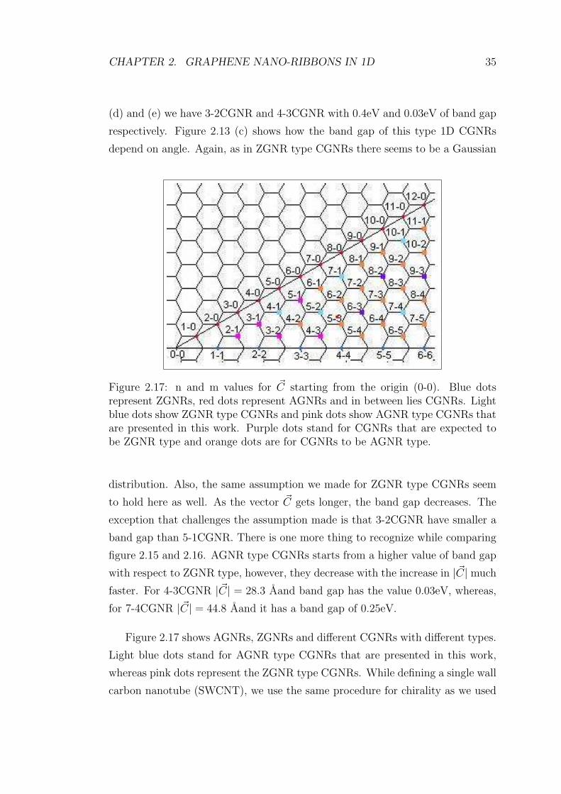
2.17 n and m values for ~C starting from the origin (0-0). Blue dots
represent ZGNRs, red dots represent AGNRs and in between lies
CGNRs. Light blue dots show ZGNR type CGNRs and pink dots
show AGNR type CGNRs that are presented in this work. Purple
dots stand for CGNRs that are expected to be ZGNR type and
orange dots are for CGNRs to be AGNR type. . . . . . . . . . . 35
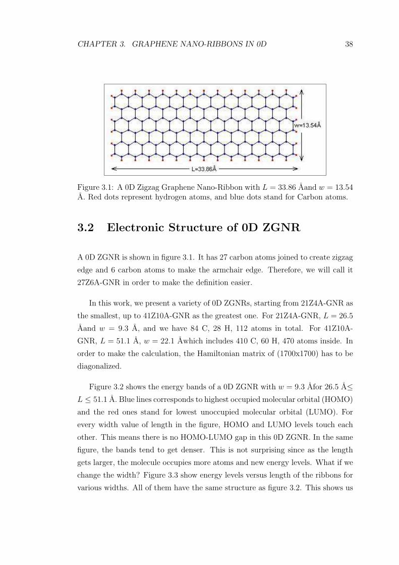
3.1 A 0D Zigzag Graphene Nano-Ribbon with L = 33.86 Aand w =
13.54 A. Red dots represent hydrogen atoms, and blue dots stand
for Carbon atoms. . . . . . . . . . . . . . . . . . . . . . . . . . . 38
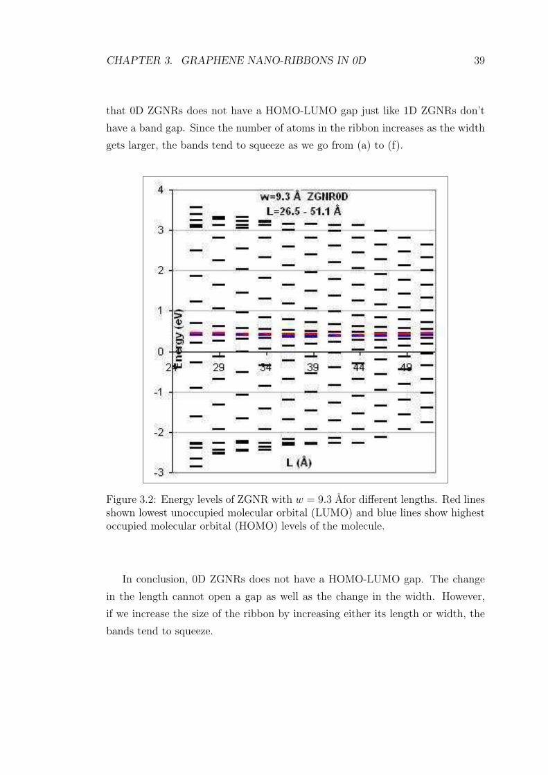
3.2 Energy levels of ZGNR with w = 9.3 Afor different lengths. Red
lines shown lowest unoccupied molecular orbital (LUMO) and blue
lines show highest occupied molecular orbital (HOMO) levels of the
molecule. . . . . . . . . . . . . . . . . . . . . . . . . . . . . . . . 39
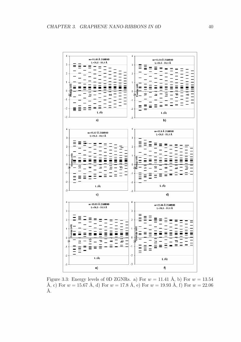
3.3 Energy levels of 0D ZGNRs. a) For w = 11.41 A, b) For w = 13.54
A, c) For w = 15.67 A, d) For w = 17.8 A, e) For w = 19.93 A, f)
For w = 22.06 A. . . . . . . . . . . . . . . . . . . . . . . . . . . . 40

LIST OF FIGURES xiii
3.4 Energy levels of 0D AGNR with width 4.33 Aversus length. Blue
lines represent HOMO levels and the red ones stand for LUMO
levels. . . . . . . . . . . . . . . . . . . . . . . . . . . . . . . . . . 41
3.5 Energy levels of various 0D AGNRs. a) For w = 6.79 A, b) For
w = 9.25 A, c) For w = 11.71 A, d) For w = 14.17 A, e) For
w = 16.63 A, f) For w = 19.09 A. . . . . . . . . . . . . . . . . . . 42
3.6 The HOMO-LUMO gap of AGNRs versus width w. L = 22.06
Afor all widths. . . . . . . . . . . . . . . . . . . . . . . . . . . . 43
3.7 (a) Energy levels versus angle α. Blue lines represent HOMO levels
and the red lines are for LUMO levels. (b) HOMO-LUMO gap
versus angle α. . . . . . . . . . . . . . . . . . . . . . . . . . . . . 45
3.8 (a) HOMO-LUMO gap of ZGNR type 0D CGNRs versus angle.
(b) HOMO-LUMO gap of AGNR type 0D CGNRs versus angle. 46
3.9 (a) Energy levels versus length of chiral vector for all 0D CGNRs.
Green energy levels represent n − m 6= 3p, whereas, black lines
stand for n − m = 3p, p being integer. (b) Energy levels versus
length of ~C for ribbons having the property that n−m is a multiple
of three. (c) Energy levels versus length of ~C for the ribbons for
which n−m is not a multiple of three. In all graphs blue lines are
HOMO and red lines are LUMO levels for that. . . . . . . . . . . 47

List of Tables
1.1 Tight binding coupling parameters for carbon (Adapted from D.
Tomanek, S. G. Louie, Phys. Rev B 37, 8327 (1988)) . . . . . . . 12
xiv

Chapter 1
Introduction
Carbon is one of the basic element which is extremely important for life on earth.
Only by looking at the role in organic chemistry, carbon can be declared as the
most important element on earth. Since it has flexibility in bonding like sp,
sp2 or sp3; many compounds including carbon show very different geometrical
and electronic structures and properties. For a physicist dealing with nano-sized
structures, geometry of the structure is greatly important, since it determines the
dimensionality [1]. (See the figure 1.1)
Graphene, for instance, is only made up of carbon atoms which is two dimen-
sional (2D), whereas carbon nanotube is a one dimensional (1D) material. The
dimensions, of course, affect most of the physical properties of the material. In
graphene, carbon atoms create a honeycomb structure with hexagons on a plane.
In carbon nanotubes these hexagons are not planar but they are rolled to create a
cylinder. In fullerenes, however, the structure is just a sphere, which makes them
zero dimensional (0D) molecules with discrete energy states. Graphite, is a three
dimensional (3D) allotrope of carbon, which is known for centuries. They are
made out of stacks of graphene layers which are weakly bound by van der Waals
forces. Therefore, graphite can be expected to have closer physical properties to
graphene. Theoretical works enlighten these expectations, however, experimental
works can recently be done since graphene could not be obtained as a single layer
until 2004 [2]. After this date, the importance of graphene once more realized
1

CHAPTER 1. INTRODUCTION 2
and many researchers started to examine it again.
Figure 1.1: Structures of Carbon with different dimensions. a) Graphene consistsof honeycomb lattice of carbon atoms in 2D, b) Graphite is a stack of graphenelayers creating a 3D structure, c) Carbon Nanotubes are rolled-up cylinders ofgraphene in 1D and d) Fullerenes (C60) are molecules consisting of wrappedgraphene by introduction of pentagons on honeycomb lattice in 0D. Grapheneis mother of them all.
Graphene nano-ribbons are structures with a rectangular shape which are cut
from graphene sheet. Since they have finite width and length, in nano scale, they
are considered to be 0D structures. They can have different physical properties
depending on their width, length and chirality. If we consider the length to be
CHAPTER 1. INTRODUCTION 3
infinite, they become 1D structure [3,4]. There are theoretical works in the liter-
ature on both 1D and 0D graphene nano-ribbons, however, they mostly consider
either very small width and length to have a small number of carbon atoms in-
cluded, which cannot be created experimentally for quite long time, or ribbons
with large width but infinitely long length which is not what is aimed. There is
even no work in the literature that deals with chirality of the ribbons. This work
presents the electronic structure of graphene nano-ribbons with large width and
finite length. Also, the chiral nano ribbons are also included. The calculations
are made by using tight binding method. The reason to use tight binding method
is that it is fast and reliable for this calculation, and it can deal with many atoms
at once, which other methods cannot.
1.1 Tight Binding Method
The tight-binding (TB) model is a kind of counterpart of the nearly-free elec-
tron approximation. The approximation of the TB method assumes that the
restricted Hilbert space, spanned by atomic-like orbitals is sufficient to describe
the wave functions solution of the Schrodinger equation (at least in restricted
energy range). Such an atomic-like basis provides a natural, physically moti-
vated description of electronic states in matter [5]. In tight binding calculations,
due to the translational symmetry, any wave function should satisfy the Bloch’s
Theorem [5]
T~aiΨ = ei~k·~aiΨ (1.1)
where Taiis a translational operation along the lattice vector ~ai (i = 1, 2, 3), and
~k is the wave vector. For the purpose, we define Φ(~k, ~r) as a Tight Binding Bloch
function which is given by [5]
Φj(~k, ~r) =1√N
N∑
~R
ei~k·~Rψj(~r − ~R), (j = 1, ..., n). (1.2)
~R is the position of the atom and ψj denotes the atomic wave function in state
j, N is the number of unit cells, n is the number of Bloch functions in the solid
for a given ~k. From equation 1.2, it is clear that Φj(~k, ~r + ~a) = ei~k·~a Φj(~k, ~r) so

CHAPTER 1. INTRODUCTION 4
TMai= 1 which also expresses eikMai = 1 [5]. Then the wave number k is equal to
2pπ/Mai where p = 0, 1, 2, ..., M − 1, i = 1, 2, 3. The eigenfunctions in the solid
Ψj(~k, ~r) are expressed by a linear combination of Bloch functions as follows;
Ψj(~k, ~r) =n∑
j′=1
Cjj′(~k)Φj′(~k, ~r). (1.3)
Here, Cjj′ are coefficients to be determined. The j’th eigenvalue as a function of
~k is given by;
Ej(~k) =〈Ψj|H|Ψj〉〈Ψj|Ψj〉 (1.4)
where H is the hamiltonian of the solid. Substituting equation 1.3 into equation
1.4, we obtain;
Ei(~k) =
∑nj,j′=1 Hjj′(~k)C∗
ijCij′∑n
j,j′=1 Sjj′(~k)C∗ijCij′
(1.5)
where the integrals over the Bloch orbitals, Hjj′(~k) = 〈Φj|H|Φj′〉 and Sjj′(~k) =
〈Φj|Φj′〉 (j, j′ = 1, ..., n) are called transfer integral matrices and overlap integral
matrices respectively. If we minimize the eigenvalue by taking derivative with
respect to C∗ij and use it in equation 1.5, we have the generalized eigenvalue
equation
HCi = Ei(~k)SCi, (1.6)
where Ci is defined as a column vector with elements Ci1, ..., CiN . By trans-
porting the right hand side to the left we have either Ci = 0, which represents
the null vector, or secular equation as follows;
det|H − ES| = 0. (1.7)
By solving the secular equation, one can have the eigenvalues which are energy
values Ei(~k), (i = 1, ..., n) for a given ~k [5].
1.2 Electronic Properties of Graphene
Graphene can be defined as single layer of graphite. Although it is a 2D material
the electronic structure does not differ much from graphite. This is because

CHAPTER 1. INTRODUCTION 5
Figure 1.2: Carbon atoms are located at the corners of the hexagons. Blue dotshows A type and black dots show three nearest B type atoms. Red arrows arelattice vectors ~a1 and ~a2
even for graphite, interactions between the layers are very weak since layer to
layer distance is 3.35 A, which is more than twice the interatomic bond distance
between carbon atoms in the single layer. Graphite has been known by human
kind since 1564, the invention of pencil. Although it is known for 444 years,
the experimentalists have recently been able to investigate one atom thick flakes
among the pencil debris [1]. Therefore, single layer of graphite could be isolated
in 2004.
In graphene, carbon makes sp2 hybridization. One s orbital (one 2s orbital)
combines with two p orbitals (two 2p) which leads a trigonal planar structure.
Carbons make σ bonds with each other. They are separated with a distance
of 1.42 A. If we put graphene layers one above another there occurs a π bond
between them leading to the formation of graphite. Last remaining electron in
2p orbital is responsible for this π bond which is not related to sp2 hybridization.
Since in graphene there is an unaffected p orbital perpendicular to the planar
structure, each carbon has one extra electron and π band is half filled.
CHAPTER 1. INTRODUCTION 6
With tight binding approach, electronic structure of graphene can be exam-
ined and explained very easily. Since carbon atoms make hexagonal structure,
it can be seen as a triangular lattice. If we choose the distance between carbon
atoms as a, the lattice vectors can be written as [1];
~a1 =a
2(3,√
3) (1.8)
~a2 =a
2(3,−
√3). (1.9)
If one generates a lattice with these lattice vectors to make a graphene, there
are two atoms inside the unit cell, atom A and atom B. Both of these atoms are
carbon atoms of course and there is no difference between them except for the
definition of positions.
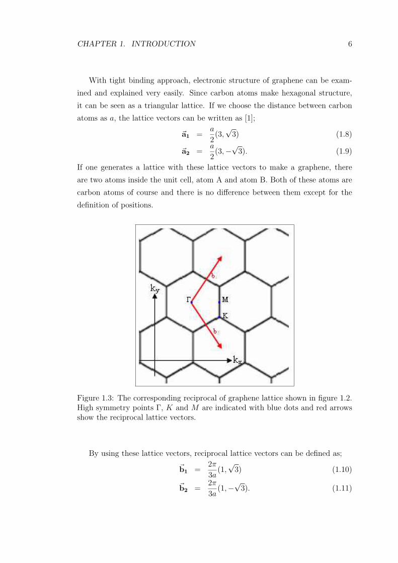
Figure 1.3: The corresponding reciprocal of graphene lattice shown in figure 1.2.High symmetry points Γ, K and M are indicated with blue dots and red arrowsshow the reciprocal lattice vectors.
By using these lattice vectors, reciprocal lattice vectors can be defined as;
~b1 =2π
3a(1,√
3) (1.10)
~b2 =2π
3a(1,−
√3). (1.11)
CHAPTER 1. INTRODUCTION 7
In the Brillouin zone of graphene, there are three special points, that ease
the problem of determining the electronic structure. These points are so called
high symmetry points which are Γ, K and M . The positions of these points in
momentum space can be defined as (see figure 1.3);
Γ = (0, 0) (1.12)
K = (2π
3a,± 2π
3√
3a) (1.13)
M = (2π
3a, 0). (1.14)
Putting atom A at the origin in real space the three nearest neighbours are located
at;
δ1 =a
2(1,√
3) (1.15)
δ2 =a
2(1,−
√3) (1.16)
δ3 = a(−1, 0). (1.17)
δs are the positions of B atoms, since they are the nearest neighbours of atom A.
The six second nearest neighbours for the atom A are positioned at;
δ′1 =a
2(3,√
3) (1.18)
δ′2 =a
2(3,−
√3) (1.19)
δ′3 = a(0,−√
3) (1.20)
δ′4 =a
2(−3,−
√3) (1.21)
δ′5 =a
2(−3,
√3) (1.22)
δ′6 = a(0,√
3). (1.23)
To calculate the band structure of graphene by using tight binding method we
have to construct the hamiltonian matrix H. For simplicity of explanation, first
nearest neighbour approach can be used. Then, to calculate π bands there is only
an integration over a single atom in HAA and HBB. Thus, HAA=HBB=ε2p for
the diagonal elements of 2x2 Hamiltonian matrix. For off diagonal elements, we

CHAPTER 1. INTRODUCTION 8
have to use first nearest neighbour positions as follows [5];
HAB = t(ei~k·~δ1 + ei~k·~δ2 + ei~k·~δ3) = tf(k) (1.24)
where t is the transfer integral between p orbitals of atom A and atom B, ~k is
the wave vector that we consider and f(k) is a function of the sum of the phase
factors of ei~k·δj (j=1,2,3). Using x and y coordinates in figure 1.2, f(k) is given
by;
f(k) = e−ikxa + 2eikxa/2 cos(kya√
3/2). (1.25)
Since f(k) is a complex function and hamiltonian matrix should be hermitian, we
write HAB = H∗AB, where ∗ denotes complex conjugate. Then, the Hamiltonian
matrix can be written in matrix form as;
H =
ε2p tf(k)
tf(k)∗ ε2p
. (1.26)
To solve the secular equation det(H − ES) = 0 we need the overlap matrix S.
For this problem overlap matrix is the following;
S =
1 sf(k)
sf(k)∗ 1
(1.27)
where s is the overlap integral that tells us about the quantity of the overlapping.
Then, the eigenvalues of E(~k) can be obtained as a function of ~k, t and s as
shown in equation 1.28.
E(~k) =ε2p ± t
√|f(~k)|2
1± s√|f(~k)|2
(1.28)
where + signs in both numerator and denominator go together to obtain bonding
π energy band, whereas minus signs indicate the anti-bonding π band. Using
ε2p = 0, t = −3.033eV, s = 0.129eV in equation 1.28, we can obtain the following
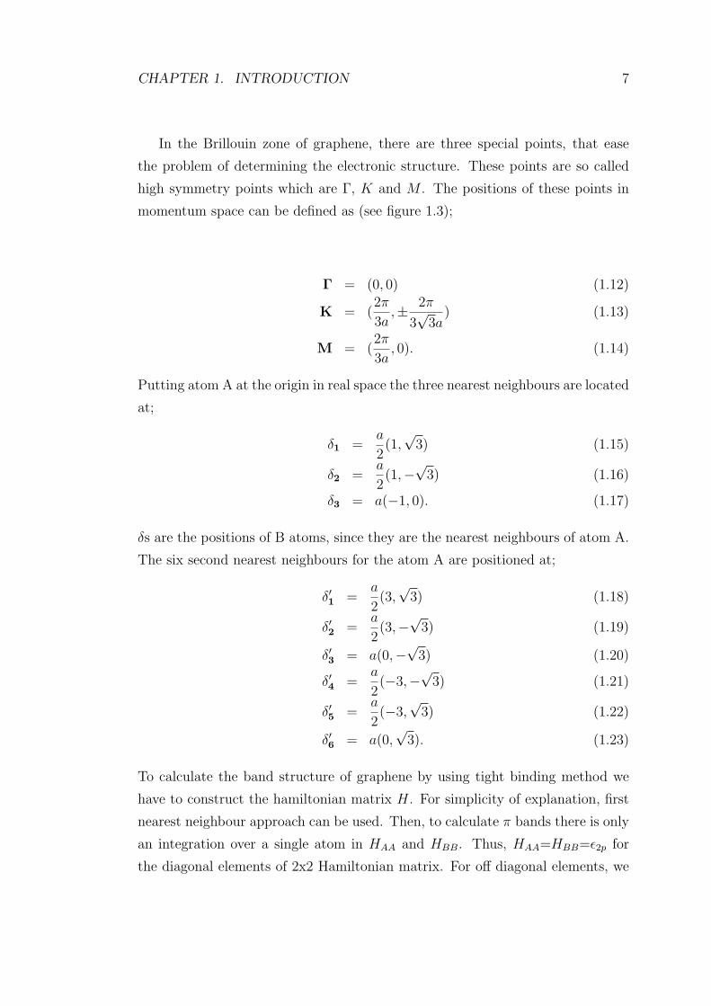
energy dispersion relation graph, figure 1.4 [5]. When the overlap integral s
becomes zero, the π and π∗ bands become symmetric around E = ε2p.
E(~k) = ±t{1 + 4 cos(3kxa
2) cos(
kya√
3
2) + 4 cos2(
kya√
3
2)}1/2 (1.29)
In this case the energies at Γ, K and M are ±3t, 0 and ±t respectively.
CHAPTER 1. INTRODUCTION 9
Figure 1.4: (a) The energy dispersion relations for graphene shown throughoutthe whole region of Brillouin zone. (b) The energy dispersion along the highsymmetry directions of the triangle ΓMK. (Reproduced from G. Dresselhaus, M.S. Dresselhaus, and R. Saito, Physical Properties of Carbon Nanotubes, ImperialCollege Press, London, 1998.)
In order to calculate σ bonds of graphene we have to consider a 6x6 Hamilto-
nian matrix. This is because, now we have to deal with 3 hybrid sp2 bonds. In
fact, for the first nearest neighbour approximation many elements in the matrix
are zero. New hamiltonian can be shown in the matrix form as;
H =
ε2s 0 0 〈2sA|2sB〉 〈2sA|2pxB〉 〈2sA|2pyB〉0 ε2p 0 〈2pxA|2sB〉 〈2pxA|2pxB〉 〈2pxA|2pyB〉0 0 ε2p 〈2pyA|2sB〉 〈2pyA|2pxB〉 〈2pyA|2pyB〉
〈2sB|2sA〉 〈2sB|2pxA〉 〈2sB|2pyA〉 ε2s 0 0
〈2pxB|2sA〉 〈2pxB|2pxA〉 〈2pxB|2pyA〉 0 ε2p 0
〈2pyB|2sA〉 〈2pyB|2pxA〉 〈2pyB|2pyA〉 0 0 ε2p
.
(1.30)
Since it is a hermitian matrix, the eigenvalues, which are energy values, are real as
it should be. To calculate the overlapping of the orbitals, we have to decompose
the wavefunctions into its σ and π components along the relevant bond. For
|2s〉 there is no such decomposition, however, |2px〉 has. As an example, we can
calculate two elements [(1,5) and (3,5)] of the hamiltonian matrix. To calculate

CHAPTER 1. INTRODUCTION 10
(1,5), we need 〈2sA| and three |2pxB〉 from three nearest neighbours. Three bonds
of atom A with B atoms have different directions, so we have to decompose |2pxB〉to σ and π components along the relevant bond. If we consider the atoms in figure
1.2, we can see that atom A makes bonds with B1 and B2 not along x direction,
but is has an angle of π/3. We can decompose |2pxB1〉 as follows;
|2px〉 = cos(π
3)|2pπ〉+ sin(
π
3)|2pσ〉. (1.31)
For B2 the same procedure is applied and it has the same decomposition for |2px〉.Then, we can calculate the value of (1,5) by the following equation;
〈2sA|2pxB〉 = 〈2s|{Hspσ(−eikxa + eikxa/2eikya√
3/2 sin(π/3) + eikxa/2e−ikya√
3/2 sin(π/3))|2pσ〉
+Hspπ(eikxa/2eikya√
3/2 cos(π/3) + eikxa/2e−ikya√
3/2 cos(π/3))|2pσ〉}. (1.32)
Here, Hspσ is the coupling parameter between 2s and 2pσ of atom A and B.
Similarly Hspπ is the coupling parameter for 2s and 2pπ and it is equal to zero.
Therefore, the last term in the equation above drops and we have only Hspσ
which we call Hsp here after. For the calculation of the value of the element
(3,5) in hamiltonian matrix, we need to decompose 〈2pyA| just like we did for
|2pxB〉. In the direction of the bond to both B1 and B2, it can be decomposed as;
〈2px| = sin(π/3)〈2pσ| + cos(π/3)〈2pπ|. In the direction of the bond to B3 we do
not have to decompose it, since the bond is in the x direction and wavefunctions
are perpendicular to each other resulting in zero overlapping. Then, the value of
(3,5) can be calculated as;
〈2pyA|2pxB〉 = {sin(π/3)〈2pσ|+ cos(π/3)〈2pπ|}
{Hppσ(−eikxa/2eikya√
3/2 cos(π/3) + eikxa/2e−ikya√
3/2 cos(π/3))|2pσ〉
+Hppπ(−eikxa/2eikya√
3/2 sin(π/3) + eikxa/2e−ikya√
3/2 sin(π/3))|2pσ〉}
= −√
3
2(Hppσ + Hppπ)eikxa/2 cos(kya
√3/2) (1.33)

CHAPTER 1. INTRODUCTION 11
Figure 1.5: Graphene electronic band structure and the parameters used in calcu-lation in Dresselhaus (ε2p = 0). (Adapted from G. Dresselhaus, M. S. Dresselhaus,and R. Saito, Physical Properties of Carbon Nanotubes, Imperial College Press,London, 1998.)
where Hppσ and Hppπ are coupling parameters. After determining all of the el-
ements of the Hamiltonian matrix, and choosing s=0 in overlap matrix, we can
solve the secular equation and find out the energy values for all ~k.
Energy bands of graphene is shown in figure 1.5 [5] by using the parameters of
Dresselhaus. Although this graph is drawn by using nonzero s values in overlap
matrix, it only uses first nearest neighbour approximation and does not deal with
second nearest A type atoms. In our calculation, we used the parameters shown
in table 1.1 [6] and included the second nearest neighbours. However, we assumed
that overlap matrix is an identity matrix.
Using these parameters, the calculated band structure is shown in figure 1.6.
Valance bands in figure 1.6 almost match with the valance bands given in figure
1.5 except for the two lowest σ bands in between M and K points. However, they
do not effect the electronic structure much. In conduction band, however, the
highest σ∗ band seem to differ mostly. This is due to the approximation made for
overlap matrix to be an identity matrix. The most important part of the band

CHAPTER 1. INTRODUCTION 12
Table 1.1: Tight binding coupling parameters for carbon (Adapted from D.Tomanek, S. G. Louie, Phys. Rev B 37, 8327 (1988))
First nearest Value(eV) Second nearest Value(eV)neighbour parameter neighbour parameter
εs -7.3 Hss2 -0.18εp 0 Hsp2 0
Hss -4.30 Hppσ2 0.35Hsp 4.98 Hppπ2 -0.10Hppσ 6.38Hppπ -2.66
Figure 1.6: Graphene electronic band structure calculated by using tight bindingparameters shown in table 1.1 and drawn between Γ, K and M points to comparewith figure 1.5.

CHAPTER 1. INTRODUCTION 13
structure is π and π∗ bands and they seem to match quite well. In both figures
for band structure of graphene, the valance and the conduction bands touch at
K points creating zero energy gap. This makes graphene a semi-metal. At these
Dirac points, the dispersion is conical. Near these crossing points, the electron
energy is linearly dependent on the wave vector and it is given by;
E±(q) ∼= ±vF |q|+ Θ(q2) (1.34)
where q is the momentum measured relatively to the Dirac points and vF is the
Fermi velocity [1]. According to Wallace [8], the value of this velocity is around
106 m/s, which is around c/300, c being the speed of light.
The energy spectrum of graphene resembles the energy of ultra-relativistic
particles which are quantum mechanically described by the Dirac equation. A
result of this Dirac like spectrum is, cyclotron mass. The cyclotron mass is defined
as
m∗ =1
2π
∂A(E)
∂E, (1.35)
where A(E) is the area enclosed by orbit in momentum space. A(E) is given by;
A(E) = πq2 = πE2
v2F
. (1.36)
Using 1.36 in 1.35, one can obtain
m∗ =E
v2F
=q
vF
. (1.37)
The electronic density is related to the Fermi momentum as n = k2F /π leading to
the following equation;
m∗ =
√π
vF
√n. (1.38)
Therefore, cyclotron mass depends on the square root of electronic density.
The experimental data fits very well to the calculated results providing an esti-
mation Fermi velocity around 106 m/s [1]. The experimental observation for the
dependence of cyclotron mass to√
n, provides an evidence for the existence of
massless Dirac quasi-particles in graphene.
According to Castro [1] the density of states is shown in figure 1.7 both for
first and second nearest neighbour approximation. In both cases graphene shows

CHAPTER 1. INTRODUCTION 14
semi-metallic behaviour. According to the figures that zoom to Fermi level, the
density of states changes linearly with energy, ρ(ε) ∝ |ε| [1].
Figure 1.7: Density of states of graphene computed with second nearest neighbour(top) and first nearest neighbour approximation (bottom). Also shown on theright hand side is zoom in of the density of states close to the neutrality ofone electron per site. (Taken from A. H. C. Neto, F. Guinea, N. M. R. Peres,K. S. Novoselov and A. K. Geim, arXiv:0709.1163, Rev. Mod. Phys. (to bepublished).)
1.3 Organization of the Thesis
The thesis consists of 4 chapters. First chapter is an introductory chapter which
includes the motivation of this study and a brief information about graphene. The
second chapter continues with the information, calculation, and the theoretical
results about the band structure of graphene nano-ribbons (GNRs) with various
kinds such as zigzag, armchair and chiral GNRs in 1D. These ribbons include
hydrogen atoms (hydrogens are crucial for the calculations) at the edges, which
CHAPTER 1. INTRODUCTION 15
is more realistic, to saturate the dangling bonds of carbons. The third chapter
explores the electronic structure of graphene nano-ribbons with finite length and
width for all types of ribbons (0D). This time, Hydrogens are added to both
width and length of the ribbon. In both chapter two and three various widths
are explored. Finally, the fourth chapter concludes the thesis.

Chapter 2
Graphene Nano-Ribbons in 1D
2.1 Geometry of Graphene Nano-ribbons in 1D
Graphene nano-ribbons are graphene sheets with finite size. In this section, we
will describe the ribbons of 1D which is infinitely long in one of the dimensions,
while the width is finite along the other direction. For generating a ribbon of 1D,
we have to cut 2D graphene sheet such that one side is infinitely long (uncut),
which we will define as length (L) and the other side is finite (cut in nano-scale),
which will be called as width (w) to have an infinitely long rectangular shaped
structure. The geometry of graphene nano-ribbons can be described with two
positive integers (n,m) (n > m defines all) just like defining a nanotube. These
numbers show the chirality of the ribbon. If we define the lattice shown in figure
1.2, and put the coordinate system such that atom A sits at the origin and at the
lattice point, ~C = n~a1 +m~a2 brings us to another A type atom, so another lattice
point. If we cut the graphene sheet perpendicular to the line joining these two A
type atoms (including half of both atoms), we have the lengths of the rectangle.
The width is the equal to |~C|. In figure 2.1 a zigzag type graphene nano-ribbon is
shown at the top and an armchair type is shown at the bottom side. To generate
an armchair graphene nano-ribbon (AGNR), we have n = c, c being any positive
integer and m = 0. To generate zigzag graphene nano-ribbon (ZGNR) we have
16

CHAPTER 2. GRAPHENE NANO-RIBBONS IN 1D 17
n = m = c. For any other combination of n and m (n > m), we will have a chiral
graphene nano-ribbon (CGNR). The names zigzag and armchair comes from the
shape of the length side of the ribbon. In figure 2.1, the length can be defined
Figure 2.1: a) A zigzag graphene nano-ribbon (N = 8) and b) an armchairgraphene nano-ribbon (N = 14). Red rectangles are illustrations of the unit cellsused in calculations.
from left to right and the width can be defined from bottom to the top of the
ribbon. In ZGNR, it can be seen that the length side has a zigzag arrangement
of carbon atoms, and in AGNR, the carbon atoms make an armchair shape. In
CGNR there is no specific type of arrangement. The numbers 1,2,3,...N at the
right hand side of each ribbon in figure 2.1 is a definition of the width of the
ribbon. If one talks about 10ZGNR, it means that in the top picture of figure
2.1, N = 10, so we have 10 carbon atoms along the width. The same is also true
for AGNR.
CHAPTER 2. GRAPHENE NANO-RIBBONS IN 1D 18
In the calculation of the band structure of 1D ribbons, we take a unit cell
(black rectangles in figure 2.1). Since the ribbon is infinitely long, the cell is re-
peated infinitely both in the right and left hand side of the rectangles. Therefore,
all carbon atoms except for the ones in the first and N’th rows have three carbon
atoms around. The ones at the edges (at the first and N’th row), have two carbon
atoms nearby and the third sp2 bond does not occur creating a dangling bond
and making the calculation of the electronic structure difficult and misleading.
Therefore, for the saturation of the dangling bonds we had to add some atoms
or molecules. The easiest and mostly used atom was hydrogen [10,11,12,13,14] ,
so we added hydrogen atoms instead of the third carbon atom at the edges. We
took the distance between carbon atom and the hydrogen atom that bounded to
it to be 1.09 A. In the calculation of 1D CGNR, we again need a unit cell that
repeats itself infinitely long. In order to find how the unit cell can be formed,
we have a simple operation. This operation requires the definition of chirality,
the numbers n and m. The vector ~C joins one lattice point to another. To have
a unit cell we need another vector that starts from the same lattice point as ~C,
goes perpendicular to it and ends up in another lattice point. Such a vector can
be defined as ~T = p~a1 + q ~a2, where p and q are integers that will be defined with
the help of n and m. To find p and q we define a number d which is the greatest
common divisor of 2n+m and 2m+n. Now that we defined d, we can have p and
q as follows [15];
p =2m + n
d(2.1)
q = −2n + m
d. (2.2)
Figure 2.2 shows the unit cell of a 1D CGNR where n = 4 and m = 1. Here,
greatest common divisor of 2n + m = 9 and 2m + n = 6 is d = 3. Therefore,
p = 6/3 = 2 and q = −9/3 = 3. So ~T = 2~a1 − 3~a2. With the reputation of unit
cell along ~T infinitely many times, we have 1D 4-1 CGNR.
For the tight binding calculation, we need some more parameters as we added
hydrogen atoms in the system. These parameters should include hydrogen-carbon
interaction and hydrogen self energy. We do not need hydrogen-hydrogen in-
teraction since they will be too far away from each other to have a noticeable

CHAPTER 2. GRAPHENE NANO-RIBBONS IN 1D 19
Figure 2.2: A Chiral Graphene Nano-Ribbon. a1 and a2 are unit vectors, red lineshows ~C = 4~a1 +1~a2, and dark blue line represents ~T = 2~a1−3~a2, these two lineswith light blue ones enclose the unit cell of 4-1 CGNR. α is the chiral angle.
contribution. Also, these new parameters should be consistent with the ones
we use for carbon atoms. We need three new parameters showing hydrogen self
energy, the interaction between s orbital of hydrogen and s orbital of carbon
and the interaction between s orbital of hydrogen and p orbital of carbon. To
calculate these parameters we made a fitting program for three molecules CH,
CH4 and C2H4 all of which include only hydrogens and carbons [16,17,18,19,20].
This fitting program generated the necessary three parameters including the ones
shown in table 1.1. These new parameters are; εH = 6.85eV , HHs−Cs = 7.66eV ,
HHs−Cp = −9.92eV for a distance of 1.09A between hydrogen and carbon atoms.
The generated band structures of hydrogen added graphene nano-ribbons have a
good agreement with the ones in the literature. Band structures of 1D GNRs is
discussed in the following sections.
2.2 Electronic Structure of 1D ZGNR
For ZGNR, the length side has zigzag shape and the width side has armchair
shape. The hydrogens are added to the first and N’th row carbon atoms as

CHAPTER 2. GRAPHENE NANO-RIBBONS IN 1D 20
shown in figure 2.3.
Figure 2.3: A hydrogenated zigzag graphene nano-ribbon. Red dots representsthe hydrogen atoms.
In this work we calculated the band structure of 1D ZGNRs up to N=150.
There is not much work in the literature with such a huge width up to now. At
this width, the calculation includes 302 atoms, two of which are hydrogen atoms.
To calculate the band structure of such a ribbon we have to find the eigenvalues
of the hamiltonian matrix (see Section 1.3) of size (1202x1202) at each ~k point.
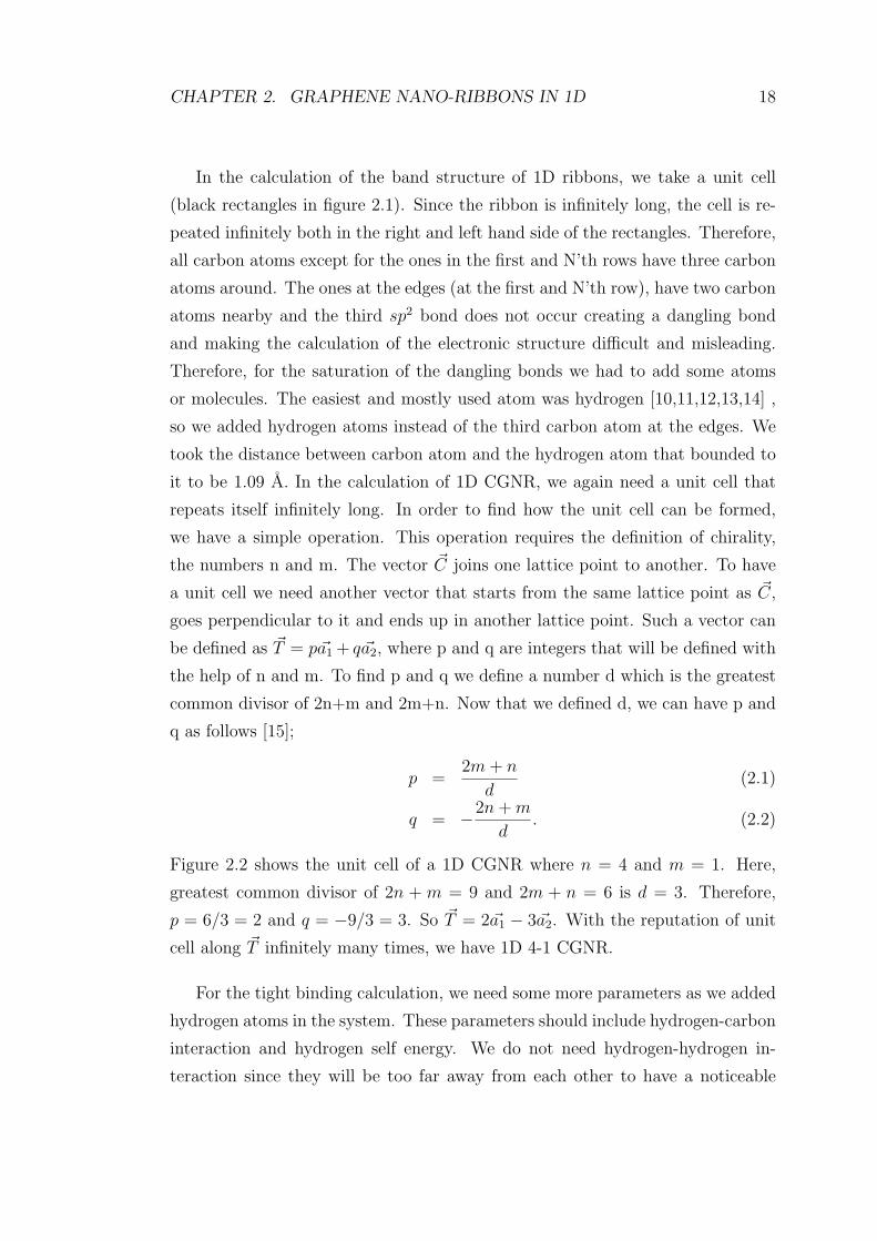
Figure 2.4 [10] shows a comparison of calculated band structure 1D 10ZGNR
with the one in the literature. Although everything related to the calculation
of the bands is different, the similarities in band structure are obvious. Red
lines represent the valance bands, whereas blue ones stand for conduction bands.
Valance and conduction bands touch each other after K point and the two states
become degenerate up to M point. Other conduction bands become degenerate
at M point just like the valance bands. At Γ point we have a band gap around 7
eV in both graphs. Also some bands, marked with green dots, does not obey the
general trend. Some of these bands in conduction band could not be observed,
however, in valance band we have more or less the same behaviour of the bands.
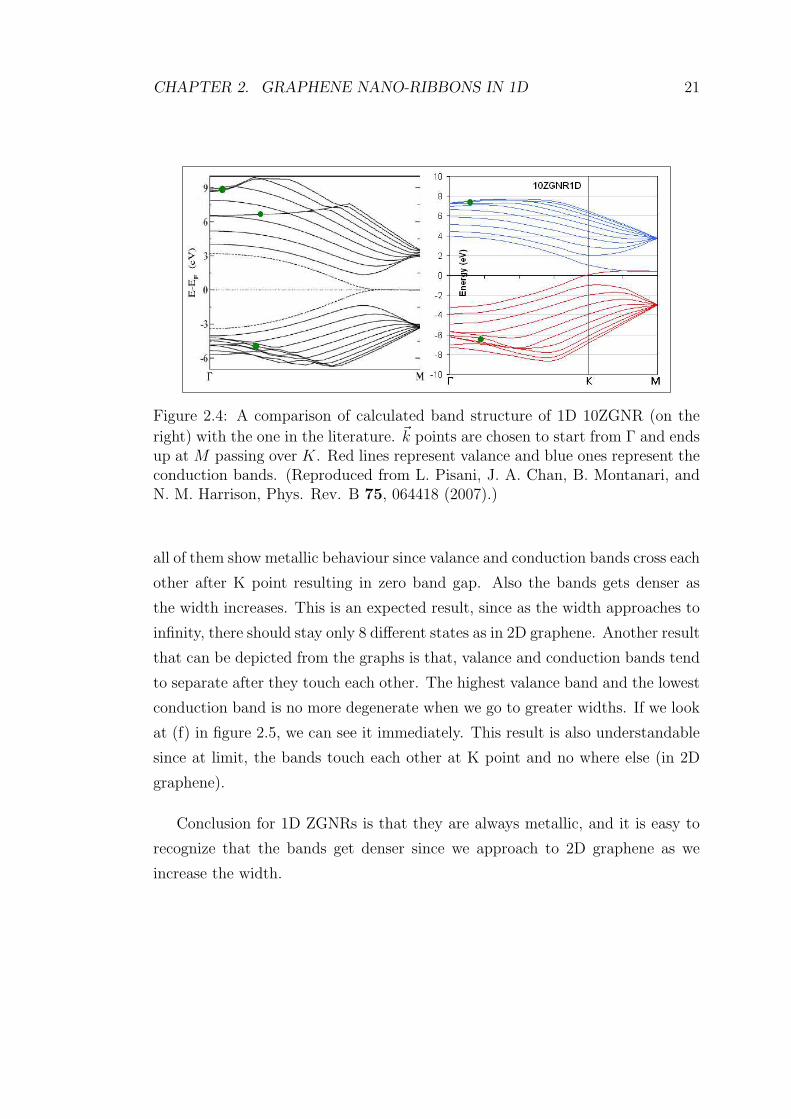
In figure 2.5, band structures of various ZGNRs in 1D is shown. 30ZGNR has a
width of 6.32 nm and 150ZGNR has 31.9 nm as a width. The easiest to recognize,
CHAPTER 2. GRAPHENE NANO-RIBBONS IN 1D 21
Figure 2.4: A comparison of calculated band structure of 1D 10ZGNR (on the
right) with the one in the literature. ~k points are chosen to start from Γ and endsup at M passing over K. Red lines represent valance and blue ones represent theconduction bands. (Reproduced from L. Pisani, J. A. Chan, B. Montanari, andN. M. Harrison, Phys. Rev. B 75, 064418 (2007).)
all of them show metallic behaviour since valance and conduction bands cross each
other after K point resulting in zero band gap. Also the bands gets denser as
the width increases. This is an expected result, since as the width approaches to
infinity, there should stay only 8 different states as in 2D graphene. Another result
that can be depicted from the graphs is that, valance and conduction bands tend
to separate after they touch each other. The highest valance band and the lowest
conduction band is no more degenerate when we go to greater widths. If we look
at (f) in figure 2.5, we can see it immediately. This result is also understandable
since at limit, the bands touch each other at K point and no where else (in 2D
graphene).
Conclusion for 1D ZGNRs is that they are always metallic, and it is easy to
recognize that the bands get denser since we approach to 2D graphene as we
increase the width.
CHAPTER 2. GRAPHENE NANO-RIBBONS IN 1D 22
Figure 2.5: Calculated band structures starting from 30ZGNR up to 150 ZGNR in1D. a) Band structure of 30ZGNR b) Band structure of 60ZGNR c) Band struc-ture of 90ZGNR d) Band structure of 120ZGNR e) Band structure of 150ZGNRf) A zoomed piece of (e) showing the portion between K and M points.

CHAPTER 2. GRAPHENE NANO-RIBBONS IN 1D 23
2.3 Electronic Structure of 1D AGNR
For AGNR, the length side has armchair shape and the width side has zigzag
shape. The hydrogens are added to the first and N’th row carbon atoms as
shown in figure 2.6.
Figure 2.6: A hydrogenated armchair graphene nano-ribbon. Red dots representsthe hydrogen atoms.
In this work we calculated the band structures of 1D AGNRs up to N = 151.
At such a huge width for a graphene nano-ribbon (GNR), we have 306 atoms in
the unit cell 4 of which are hydrogen atoms. Figure 2.7 shows a comparison of
the bands structures that we calculated with the ones in the literature [11] for
12AGNR, 13AGNR and 14AGNR. There are 3 different groups to compare. The
reason for three different groups will be explained later. Looking at figure 2.7
(a), and compare it with (b), we can say that band structures are pretty similar
to each other. Band gaps are around 0.7eV around Γ point in both graphs. The
behaviour of bands are almost the same, and also the crossings of the bands shown
as green dots occur more or less in the same way. When we compare 13AGNRs,
although band gap is around 0.8eV in both graphs (c) and (d), and the bands

CHAPTER 2. GRAPHENE NANO-RIBBONS IN 1D 24
Figure 2.7: Band structures of N = 12,13 and 14 AGNRs. Band structures ofa)N = 12, c)N = 13, e)N = 14 AGNRs from the literature. Calculated bandstructures of b)N = 12, d)N = 13, f)N = 14 AGNRs. (Reproduced and adaptedfrom [Young-Woo Son, et.al. PRL 97, 216803 (2006)])
CHAPTER 2. GRAPHENE NANO-RIBBONS IN 1D 25
behave the same way, there is a problem with some of the crossings of the bands
shown as green dots. But the general structure is generated. When we come to
N = 14 AGNRs, we see that the structure is almost perfectly generated except
for one of the green dots. At (e) it seems there is a tiny band gap, however, band
gap should be zero in a tight binding calculation as the author of the same paper
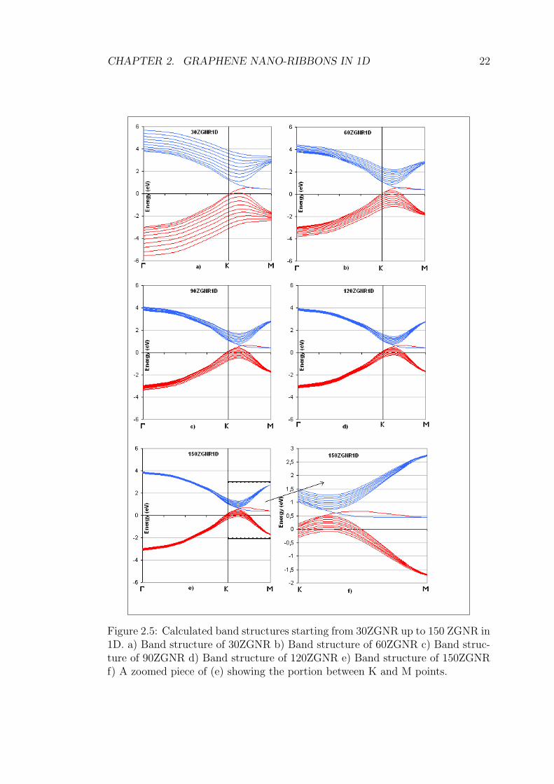
suggests in figure 2.8 [11].
Figure 2.8: Comparison of band gap of 1D AGNRs versus width calculated, withthe one in the literature. There are 3 main groups, 3N , 3N +1 and 3N +2 shownas blue dots, red squares and pink triangles respectively. (Adapted from Y.-WSon, M. L. Cohen, and S. G. Louie, Phys. Rev. Lett. 97, 216803 (2006).)
Figure 2.8 shows three groups for the width two of which behave the same
way. If we have pAGNR and p is equal to 3N or 3N + 1, N being an integer; we
have an AGNR with a band gap. Since 12 = 3 ∗ 4 and 13 = 3 ∗ 4 + 1 (p = 4), we
have a ribbon with a band gap as indicated in figure 2.7 (b) and (d). However,
since 14 = 3 ∗ 4 + 2, we have zero band gap in figure 2.7 (f). The two graphs in
figure 2.8 are in pretty good agreement. For AGNRs with a band gap, when the
width is greater than 10 A, the band gap decreases below 1eV. When the width
reaches to 25 A, the band gap decreases to 0.5eV. When the width becomes 40
A, the band gap is around 0.3eV in both graphs. The main idea of the figures is
that 1D AGNRs have zero band gap if we have a width such that p = 3N + 2,
and have a finite band gap if p 6= 3N + 2 [11,21]. Another result that can be
depicted from the figures is that the band gap decreases as the width increases.

CHAPTER 2. GRAPHENE NANO-RIBBONS IN 1D 26
Figure 2.9: Band structure of 1D AGNRs with various widths. All of them havea width of type 3N + 2.
CHAPTER 2. GRAPHENE NANO-RIBBONS IN 1D 27
What happens if we have much greater 1D AGNRs? Figure 2.9 show greater
1D AGNRs of type 3N + 2. As it can be seen all of them have zero band gap.
They all obey the 3N + 2 type behaviour. Also, the bands tend to get denser
as the width increases. This is an expected result since at limit, we will end up
with 8 different bands as in 2D graphene. However, in 2D graphene valance and
conduction bands does not touch at Γ point. Instead, they become degenerate
at K point as shown in figure 1.6. Therefore, somehow, at limit the valance
and conduction bands have to separate at Γ point to satisfy the condition for
2D graphene. Since our periodicity is in one direction, we cannot see this effect
whatever the width is.
Figure 2.10 shows the band structures of 3NAGNRs (on the left) and 3N +
1AGNRs (on the right) as a function of width. All of the band structures (a-h)
have a band gap which decreases as the width increases. Also, as the width gets
larger, the bands become denser just like the previous band structures did. In
fact, there is no satisfactory reason to make a distinction between 3NAGNRs and
3N +1AGNRs. Therefore, we have two distinct groups as 3N +2AGNRs and the
remaining ones, for 1D AGNRs. It will be clearer if we look at figure 2.11 that
we cannot separate 3N type and 3N + 1 type AGNRs. In this figure, almost all
of the red squares are on top of blue dots showing the same band gap for 3N and
3N + 1 AGNRs.
In figure 2.11 the width starts from 50AGNR (60.26 A) and goes up to
151AGNR (184.5 A). These AGNRs are much more greater than we presented
previously. It is not so easy to obtain even 2D graphene experimentally. There-
fore, it will be too difficult to cut it as small as 10-20AGNR (around 20 A). That’s
why 50-150AGNRs are much more realistic and important than smaller ones for
now. Although they are important, they have a band gap smaller than 0.25eV
decreasing their capability to be used as semiconductor devices for applications.
After w > 100 A, we have a band gap less than 0.15eV and even smaller than
0.1eV for w > 150 A. It gets smaller and smaller as the width gets larger.
In conclusion, 1D AGNRs can be classified in two different groups. One of
the groups is 3N + 2 group in which all ribbons are semi-metal having zero band

CHAPTER 2. GRAPHENE NANO-RIBBONS IN 1D 28
Figure 2.10: Band structure of 1D AGNRs with various widths. Graphs on theleft hand side have a width of type 3N , and graphs on the right hand side havea width of type 3N + 1.

CHAPTER 2. GRAPHENE NANO-RIBBONS IN 1D 29
gap since valance and conduction bands touch each other at Γ point. The second
Figure 2.11: Band gaps of 1D AGNRs of three types as a function of width. 3N ,3N +1 and 3N +2 shown as blue dots, red squares and pink triangles respectively.
group is the rest of AGNRs (3N and 3N + 1) in which all ribbons have a finite
band gap showing semiconducting behaviour. The band gaps of this second group
members tend to decrease as the width increases. Calculations show that they
get below 0.1eV as the width gets above 150 A.
2.4 Electronic Structure of 1D CGNR
CGNRs are graphene nano-ribbons that do not have an edge in zigzag or armchair
shape. In fact they can have various shapes depending on the chirality. CGNRs
can be defined with two positive integers n and m (n > m). When m equal to n
we have a ZGNR in which vector ~C = n~a1 + m~a2 is parallel to x axis, and when
m equal to zero we have an AGNR in which vector ~C makes an angle of π6
with

CHAPTER 2. GRAPHENE NANO-RIBBONS IN 1D 30
x axis. Therefore, in all CGNRs, ~C makes an angle 0 < α < π/6 with the x axis
as shown in figure 2.2. The region π/6 < α < π/3 is the reputation of the same
CGNRs in reverse order (from ZGNR to AGNR).
CGNRs are important because there is no work about them in the literature.
Calculations related to CGNRs will be one of the most important contributions
that we will make to the literature. Figure 2.12 shows the unit cell of 10-1CGNR.
Since n = 10 and m = 1, d, p and q can be calculated as d = 3, p = 4 and
q = −7 by using equations 2.1 and 2.2. This can also be checked by looking at
the figure. Vector ~C makes an angle with x axis α = 25.28o. Since we have 148
Figure 2.12: Unit cell of 1D 10-1CGNR is shown. Blue dots represents 148 Carbonatoms, and red dots represents 14 Hydrogen atoms. The unit cell repeats itselfalong non-hydrogenated carbon atoms.
carbon and 14 hydrogen atoms inside the unit cell, the calculation includes 162
atoms, which is not the greatest one that we calculated. The smallest CGNR is
4-1 CGNR (shown in figure 2.2) which has 28 carbon and 6 hydrogen atoms in
its unit cell.
If we think of the angle although 10-1CGNR is close to be an AGNR, it has

CHAPTER 2. GRAPHENE NANO-RIBBONS IN 1D 31
a very different band structure. Figure 2.14 shows the band structure of 1D 10-
1CGNR. It is quite different from any figure of AGNRs such as the ones in figure
2.10. Valance and conduction bands are farthest at Γ point and closest at ~k = π
|~T |opposing to the band structure of AGNRs. In fact, the structure much more looks
like the band structure of ZGNRs. However, for 10-1CGNR, there is a band gap
of 0.3eV, which does not occur in a ZGNR. Therefore, the angle α seem not to
have a major effect on the band structure. May be, it can have an effect on the
value of band gap. Figure 2.13 (a) shows how band gap of 1D CGNRs change
with angle α. There are oscillations in the value of band gap as the angle changes
from zero to 30o. However, there is no straight forward dependence.
Figure 2.13: (a) Band gap versus Angle 1DCGNR for all CGNRs. (b) Band gapversus Angle for ZGNR type 1DCGNRs. (c) Band gap versus Angle for AGNRtype 1DCGNRs.
There are two types of different band structures for CGNRs. One of them can
be called ZGNR type just like the band structure of 10-1CGNR and AGNR type

CHAPTER 2. GRAPHENE NANO-RIBBONS IN 1D 32
which we will deal later. The CGNRs shown in figure 2.15 are the ones that are
ZGNR type. In the figure, 4-1CGNR, 7-4CGNR, 5-2CGNR and 7-1CGNR are
shown in (a),(b),(c) and (d) respectively. They have similar band structures but
also they have different band gaps. 4-1CGNR has a band gap of 0.6eV, while 5-
2CGNR has the second greatest with 0.45eV among this type CGNRs. 7-1CGNR
has 0.4eV, 10-1CGNR has 0.3eV and 7-4CGNR has 0.25eV of band gap.
For 4-1CGNR α = 19.1o, 5-2CGNR α = 13.9o, 7-1CGNR α = 23.4o, 10-
1CGNR α = 25.3o and 7-4CGNR α = 8.9o as shown in figure 2.13 (b). The
figure show it clearly that ZGNR type CGNRs can have a dependence on angle.
Figure 2.14: Band structure of 1D 10-1CGNR. Energy eigenvalues versus ~k points.
As we go from zero to 30o, the band gap increases at first, makes a peak and then
slowly decreases making a Gaussian like distribution. The sum of n and m, seems
to have a proportionality with band gap. For 4-1CGNR, 5-2CGNR, 7-1CGNR,
10-1CGNR, 7-4CGNR n + m = 5, 7, 8, 11, 11 respectively. By looking at this
result it can be depicted as the sum n + m increases, the band gap decreases.

CHAPTER 2. GRAPHENE NANO-RIBBONS IN 1D 33
Since the length of the vector ~C is almost proportional to the sum of n and m,
the same idea can be applied for the length of ~C. As the length of ~C increases,
the band gap decreases for ZGNR type CGNRs.
Figure 2.15: Band structures of various ZGNR type CGNRs. a)4-1CGNR, b)7-4CGNR, c)5-2CGNR, d)7-1CGNR
The second type of CGNRs were said to be AGNR type which are shown
in figure 2.16. When we look at the band structures, we can recognize that
they are much more like the band structure of 1D AGNRs as shown in figure
2.7. Here, as we go from (a) to (e), the band gap decreases. In figure 2.16 (a),
2-1CGNR is shown with a band gap of 1.3eV. In (b), we have 3-1CGNR with
1.1eV of band gap and in (c) 5-1CGNR with a band gap of 0.65eV. Finally in

CHAPTER 2. GRAPHENE NANO-RIBBONS IN 1D 34
Figure 2.16: Band structures of various AGNR type CGNRs. a)2-1CGNR, b)3-1CGNR, c)5-1CGNR, d)3-2CGNR, e)4-3CGNR
CHAPTER 2. GRAPHENE NANO-RIBBONS IN 1D 35
(d) and (e) we have 3-2CGNR and 4-3CGNR with 0.4eV and 0.03eV of band gap
respectively. Figure 2.13 (c) shows how the band gap of this type 1D CGNRs
depend on angle. Again, as in ZGNR type CGNRs there seems to be a Gaussian
Figure 2.17: n and m values for ~C starting from the origin (0-0). Blue dotsrepresent ZGNRs, red dots represent AGNRs and in between lies CGNRs. Lightblue dots show ZGNR type CGNRs and pink dots show AGNR type CGNRs thatare presented in this work. Purple dots stand for CGNRs that are expected tobe ZGNR type and orange dots are for CGNRs to be AGNR type.
distribution. Also, the same assumption we made for ZGNR type CGNRs seem
to hold here as well. As the vector ~C gets longer, the band gap decreases. The
exception that challenges the assumption made is that 3-2CGNR have smaller a
band gap than 5-1CGNR. There is one more thing to recognize while comparing
figure 2.15 and 2.16. AGNR type CGNRs starts from a higher value of band gap
with respect to ZGNR type, however, they decrease with the increase in |~C| much
faster. For 4-3CGNR |~C| = 28.3 Aand band gap has the value 0.03eV, whereas,
for 7-4CGNR |~C| = 44.8 Aand it has a band gap of 0.25eV.
Figure 2.17 shows AGNRs, ZGNRs and different CGNRs with different types.
Light blue dots stand for AGNR type CGNRs that are presented in this work,
whereas pink dots represent the ZGNR type CGNRs. While defining a single wall
carbon nanotube (SWCNT), we use the same procedure for chirality as we used

CHAPTER 2. GRAPHENE NANO-RIBBONS IN 1D 36
for GNR [5]. The main difference between SWCNT and GNR is that nanotubes
are the rolled up version of nano-ribbons. Therefore, for SWCNT, we have the
same n and m for the definition of chiral vector ~C. There is also a simple way
of determining whether SWCNT is metal or semi-conductor depending on these
numbers n and m. If n−m is a multiple of three, the nanotube becomes metallic,
semiconducting otherwise [22,23,24]. For CGNRs, there is a similar relationship
between the numbers n and m, and the type of band structure. If we inspect
carefully, all ZGNR type CGNRs we had presented, have the same property for
n and m that metallic SWCNTs have. In all ZGNR type CGNRs, n − m is a
multiple of three. However, in none of AGNR type CGNRs n−m is a multiple of
three. In figure 2.17 purple dots represent CGNRs that we expect to be ZGNR
type. If the expectation is true, one third of all CGNRs should be ZGNR type.
In the same figure, orange dots represent CGNRs that are expected to be AGNR
type for the same reason explained above. Two third of all CGNRs should be
AGNR type then. Another interesting similarity between SWCNTs and GNRs is
about the band gap. For a nanotube with a band gap, band gap value decreases
with the increase in radius. Since nanotubes are rolled up version of GNRs, the
radius depends on the chiral vector ~C by the following equation;
|~C| = 2πR. (2.3)
Therefore, the radius of nanotube is directly proportional to the chiral vector
with a proportionality constant (2π)−1. This fact lets us to state that as the
chiral vector in nanotube increases, the band gap decreases. This statement is
the same as the one we made for CGNRs.
In conclusion for 1D CGNRs, CGNRs can be categorized in two distinct fam-
ilies. One of them is ZGNR type and the other one is AGNR type CGNRs both
getting its name from the band structures. The band structure of ZGNR (AGNR)
type 1D CGNRs look like the band structure of ZGNRs (AGNRs). In ZGNR type
CGNRs, n−m is a multiple of three whereas for AGNR type CGNRs there is no
such relationship. CGNRs in both types have noticeable band gaps (maximum
1.3eV) decreasing with the increase in the length of chiral vector ~C. We also have
a Gaussian distribution for the band gap as a function of angle in both types.
The angle changes between 0 and 30o.
Chapter 3
Graphene Nano-Ribbons in 0D
3.1 Geometry of Graphene Nano-Ribbons in 0D
In this section, we will describe GNRs with finite width and length. Since both
sides are finite, we have to cut the graphene in both dimensions to have a rectangle
differing from 1D GNRs.
This time, since we have a 0D GNR, we have to consider it as a molecule
in a tight binding calculation and look for discrete energy eigenvalues at only Γ
point. In order to be able to make such a calculation we consider a unit cell much
greater than the size of the molecule. Then, repeating molecules have enough
empty space in between in order not to have an effect on each other. One other
important difference in the calculation of 0D GNRs is that we have a finite length,
so we have to put hydrogens in both dimensions of the rectangle. Figure 3.1 shows
a ZGNR with hydrogens on each side of the rectangle. The ribbon is called a
ZGNR since the length side has a zigzag shape. For this ribbon, L = 33.86 Aand
w = 13.86 Aincluding 162 carbon atoms shown as blue dots and 38 hydrogen
atoms represented by red dots thereby 200 atoms in total.
Bands for 0D ZGNR, 0D AGNR and 0D CGNR are presented in the following
sections.
37
CHAPTER 3. GRAPHENE NANO-RIBBONS IN 0D 38
Figure 3.1: A 0D Zigzag Graphene Nano-Ribbon with L = 33.86 Aand w = 13.54A. Red dots represent hydrogen atoms, and blue dots stand for Carbon atoms.
3.2 Electronic Structure of 0D ZGNR
A 0D ZGNR is shown in figure 3.1. It has 27 carbon atoms joined to create zigzag
edge and 6 carbon atoms to make the armchair edge. Therefore, we will call it
27Z6A-GNR in order to make the definition easier.
In this work, we present a variety of 0D ZGNRs, starting from 21Z4A-GNR as
the smallest, up to 41Z10A-GNR as the greatest one. For 21Z4A-GNR, L = 26.5
Aand w = 9.3 A, and we have 84 C, 28 H, 112 atoms in total. For 41Z10A-
GNR, L = 51.1 A, w = 22.1 Awhich includes 410 C, 60 H, 470 atoms inside. In
order to make the calculation, the Hamiltonian matrix of (1700x1700) has to be
diagonalized.
Figure 3.2 shows the energy bands of a 0D ZGNR with w = 9.3 Afor 26.5 A≤L ≤ 51.1 A. Blue lines corresponds to highest occupied molecular orbital (HOMO)
and the red ones stand for lowest unoccupied molecular orbital (LUMO). For
every width value of length in the figure, HOMO and LUMO levels touch each
other. This means there is no HOMO-LUMO gap in this 0D ZGNR. In the same
figure, the bands tend to get denser. This is not surprising since as the length
gets larger, the molecule occupies more atoms and new energy levels. What if we
change the width? Figure 3.3 show energy levels versus length of the ribbons for
various widths. All of them have the same structure as figure 3.2. This shows us
CHAPTER 3. GRAPHENE NANO-RIBBONS IN 0D 39
that 0D ZGNRs does not have a HOMO-LUMO gap just like 1D ZGNRs don’t
have a band gap. Since the number of atoms in the ribbon increases as the width
gets larger, the bands tend to squeeze as we go from (a) to (f).
Figure 3.2: Energy levels of ZGNR with w = 9.3 Afor different lengths. Red linesshown lowest unoccupied molecular orbital (LUMO) and blue lines show highestoccupied molecular orbital (HOMO) levels of the molecule.
In conclusion, 0D ZGNRs does not have a HOMO-LUMO gap. The change
in the length cannot open a gap as well as the change in the width. However,
if we increase the size of the ribbon by increasing either its length or width, the
bands tend to squeeze.
CHAPTER 3. GRAPHENE NANO-RIBBONS IN 0D 40
Figure 3.3: Energy levels of 0D ZGNRs. a) For w = 11.41 A, b) For w = 13.54A, c) For w = 15.67 A, d) For w = 17.8 A, e) For w = 19.93 A, f) For w = 22.06A.

CHAPTER 3. GRAPHENE NANO-RIBBONS IN 0D 41
3.3 Electronic Structure of 0D AGNR
A 0D AGNR has the length in an armchair and the width in zigzag shape. In
this work, we present various 0D AGNRs that have different widths and lengths.
10A3Z-GNR is the smallest AGNR that we work with in which the length side
has 10 carbon atoms and the width side has 3. It has 30 carbon and 22 hydrogen
atoms, 52 atoms in total. The greatest AGNR we present is 30A15Z-GNR which
has 450 carbon and 74 hydrogen atoms, 524 atoms in total. 10A3Z-GNR has
edges of w = 4.33 Aand L = 22.06 A, whereas 30A15Z-GNR has w = 19.09
Aand L = 64.66 Aas dimensions. In figure 3.4 energy levels of GNRs from
Figure 3.4: Energy levels of 0D AGNR with width 4.33 Aversus length. Bluelines represent HOMO levels and the red ones stand for LUMO levels.
10A3Z-GNR to 30A3Z-GNR is shown.
The width is the same for all energy levels as w = 4.33 A, however, the length
of the ribbon changes (22.06 A≤ L ≤ 64.66 A). In all cases, the ribbons have

CHAPTER 3. GRAPHENE NANO-RIBBONS IN 0D 42
Figure 3.5: Energy levels of various 0D AGNRs. a) For w = 6.79 A, b) Forw = 9.25 A, c) For w = 11.71 A, d) For w = 14.17 A, e) For w = 16.63 A, f) Forw = 19.09 A.

CHAPTER 3. GRAPHENE NANO-RIBBONS IN 0D 43
a noticeable HOMO-LUMO gap. For the smallest ribbon, the value of HOMO-
LUMO gap is 3.4eV. It drops slowly as the width increases and for the largest
ribbon of this width we have a gap of 2.9eV.
Figure 3.6: The HOMO-LUMO gap of AGNRs versus width w. L = 22.06 Aforall widths.
In figure 3.5, various AGNRs are shown with different widths. They are drawn
in the same length scale. The width increases as we go from (a) to (f). Notice
how HOMO and LUMO levels to approach each other as we increase the width.
After w = 11.71 A, we do not have a gap at all. Therefore, the gap of AGNRs
are both effected from the length and the width of the ribbon. As the size of the
ribbon gets larger, the HOMO-LUMO gap decreases. Figure 3.6 shows how the
HOMO-LUMO gap depends on width for the smallest length. It is obvious that
we do not have a gap after the width gets larger than 11.71 A. There is another

CHAPTER 3. GRAPHENE NANO-RIBBONS IN 0D 44
important result that can be depicted from the same graph. 3N + 2 rule that
1D AGNRs obey do not hold here. Although N = 5 in figure 3.5 (a), it has a
noticeable HOMO-LUMO gap and N = 9 for (c), which has almost zero gap.
As a conclusion, 0D AGNRs have HOMO-LUMO gaps depending on both
width and length. However, after width becomes larger than 11.7 A, we do not
have a gap even for the smallest length. Therefore, the width has a greater impact
on the electronic structure. Also, 3N + 2 rule that 1D AGNRs obey does not
hold in 0D AGNRs.
3.4 Electronic Structure of 0D CGNR
In this section, we present 0D chiral graphene nano-ribbons. These ribbons have
great importance in this work because no one has done anything about them
yet. We present 10 different 0D CGNRs as we did for 1D CGNRs. These are
2-1CGNR, 3-1CGNR, 4-1CGNR 5-1CGNR 7-1CGNR, 10-1CGNR, 3-2CGNR, 5-
2CGNR, 4-3CGNR and 7-4CGNR. We have 46 atoms, 18 of which are hydrogens
in the smallest CGNR (4-1CGNR), whereas 192 atoms, 42 of which are hydrogens,
in the greatest one, namely 4-3CGNR.
We discussed in section 2.4 that for 1D CGNR, we observed an angle depen-
dent behaviour if we separate them as ZGNR and AGNR type CGNRs. What
about CGNRs in 0D? Figure 3.7 (a) shows how energy levels of 0D CGNRs change
with angle α. Figure 3.7 (b) shows how the HOMO-LUMO gap of 0D CGNRs
changes with angle α for ten CGNRs we studied. By looking at these graphs, we
can say that there can be a relationship between chiral angle α and the HOMO-
LUMO gap of 0D CGNRs. If we include 0D ZGNRs as α = 0CGNRs, the gap
starts from 0eV, increases as alpha gets larger, and makes a peak around 12o as
2.14eV, after which it drops slowly and goes below 0.16eV for α > 25o. The trend
has a problem around 14o. It occurs because the ribbon that is responsible for
this point on the graph has a very long chiral vector ~C when it is compared with
other ones around that angle. If we separate CGNRs into two different types

CHAPTER 3. GRAPHENE NANO-RIBBONS IN 0D 45
Figure 3.7: (a) Energy levels versus angle α. Blue lines represent HOMO levelsand the red lines are for LUMO levels. (b) HOMO-LUMO gap versus angle α.
CHAPTER 3. GRAPHENE NANO-RIBBONS IN 0D 46
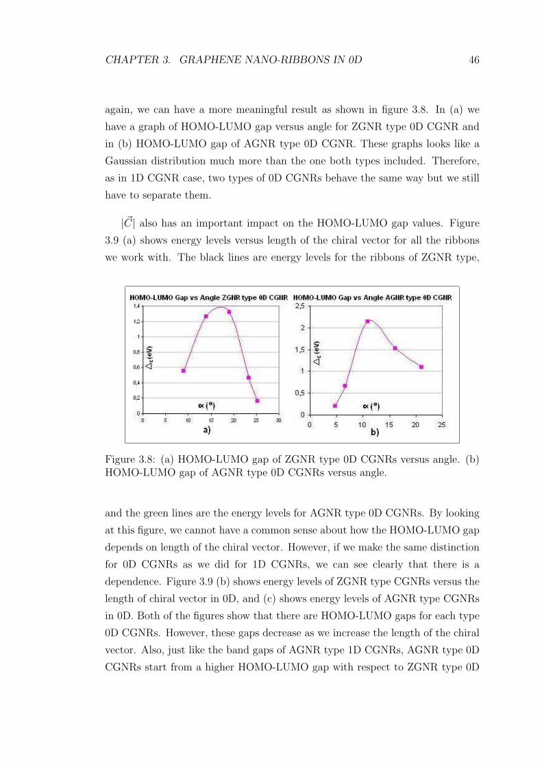
again, we can have a more meaningful result as shown in figure 3.8. In (a) we
have a graph of HOMO-LUMO gap versus angle for ZGNR type 0D CGNR and
in (b) HOMO-LUMO gap of AGNR type 0D CGNR. These graphs looks like a
Gaussian distribution much more than the one both types included. Therefore,
as in 1D CGNR case, two types of 0D CGNRs behave the same way but we still
have to separate them.
|~C| also has an important impact on the HOMO-LUMO gap values. Figure
3.9 (a) shows energy levels versus length of the chiral vector for all the ribbons
we work with. The black lines are energy levels for the ribbons of ZGNR type,
Figure 3.8: (a) HOMO-LUMO gap of ZGNR type 0D CGNRs versus angle. (b)HOMO-LUMO gap of AGNR type 0D CGNRs versus angle.
and the green lines are the energy levels for AGNR type 0D CGNRs. By looking
at this figure, we cannot have a common sense about how the HOMO-LUMO gap
depends on length of the chiral vector. However, if we make the same distinction
for 0D CGNRs as we did for 1D CGNRs, we can see clearly that there is a
dependence. Figure 3.9 (b) shows energy levels of ZGNR type CGNRs versus the
length of chiral vector in 0D, and (c) shows energy levels of AGNR type CGNRs
in 0D. Both of the figures show that there are HOMO-LUMO gaps for each type
0D CGNRs. However, these gaps decrease as we increase the length of the chiral
vector. Also, just like the band gaps of AGNR type 1D CGNRs, AGNR type 0D
CGNRs start from a higher HOMO-LUMO gap with respect to ZGNR type 0D

CHAPTER 3. GRAPHENE NANO-RIBBONS IN 0D 47
CGNRs, but drops much more quicker as we increase the length of ~C. Therefore,
Figure 3.9: (a) Energy levels versus length of chiral vector for all 0D CGNRs.Green energy levels represent n−m 6= 3p, whereas, black lines stand for n−m =3p, p being integer. (b) Energy levels versus length of ~C for ribbons having the
property that n −m is a multiple of three. (c) Energy levels versus length of ~Cfor the ribbons for which n−m is not a multiple of three. In all graphs blue linesare HOMO and red lines are LUMO levels for that.
ZGNR type 0D CGNRs have noticeable HOMO-LUMO gaps even for |~C| = 45
A(∆E = 0.55eV ), whereas, AGNR type 0D CGNRs drops to 0.2eV for |~C| = 28.3
A.
In conclusion, the electronic structure of 0D CGNRs has similarities to 1D
CGNRs. 0D CGNRs can be divided into two families as ZGNR type and AGNR
type 0D CGNRs. Both of the families have noticeable HOMO-LUMO gaps,

CHAPTER 3. GRAPHENE NANO-RIBBONS IN 0D 48
decreasing with the increase in the length of chiral vector ~C. Both of the families
show a Gaussian like distribution for the HOMO-LUMO gap as we increase the
angle of chirality. 1D CGNRs have all these properties as well.

Chapter 4
Conclusions
In this work we presented the electronic band structures of one dimensional and
zero dimensional graphene nano-ribbons. In 1D, zigzag graphene nano-ribbons
show metallic behaviour, as the valance and conduction bands touch each other
between K and M points. For 1D armchair graphene nano-ribbons however,
there are two main groups. First one is 3N + 2 group, in which all members
show a metallic behaviour as we have zero band gap at Γ point. However, in
the other group, all members show semiconducting behaviour. The band gap
for this group members decreases as the width of the ribbon increases. For 1D
chiral graphene nano-ribbons we see two distinct band structures which lets us
call the ribbons as AGNR type CGNRs and ZGNR type CGNRs depending on
the structure. In both of the families, there is band gap decreasing with the
increase in width. These two families show the same behaviour independently as
we change the chiral angle. The band gap starts from small values, reaches to
a maximum and then, goes down to small values again as we change the angle
between 0 and 30o. In 0D, ZGNRs continue to show metallic behaviour whatever
the length and width is. For 0D AGNRs, however, the width and length play a
crucial role. For small AGNRs, we have noticeable band gaps. As we increase the
width or the length, the band gap diminishes. In 0D AGNRs however, the two
distinct groups cannot be observed as in 1D case. 0D CGNRs continue to show
the same properties as if they are one dimensional. We still have two families
49

CHAPTER 4. CONCLUSIONS 50
showing the same behaviour independently. As the length of the chiral vector
increases, band gaps in both families decreases. Also, they seem to have similar
band gap distribution with the change in angle just like they had in 1D case.
This work enables us to declare that AGNRs and (especially) CGNRs in
both one and zero dimensions, can be used as semiconductors in applications.
The calculations show that the smaller the ribbon is, the larger the band gap.
Therefore, it is a strong candidate to replace silicon based transistors having a
larger band gap as it’s size gets smaller. The type, and size of the ribbon can be
arranged by considering the band gaps and conditions that are presented.
There is still much work to be done in order to improve the quality of the
calculations. The bond lengths that we assumed to be solid will not stay the same
at the edges for both carbons and hydrogens [25]. Also there can be deformation
in the structures for chiral graphene nano-ribbons due to the disordered shapes at
the edges. Next thing to do is to examine how we can get rid of these problems. If
we are able to do that, we can look forward to the changes in the band structures
when we introduce impurities or defects [26].

Bibliography
[1] A. H. C. Neto, F. Guinea, N. M. R. Peres, K. S. Novoselov and A. K.
Geim, arXiv:0709.1163, Rev. Mod. Phys. (to be published).
[2] K. S. Novoselov, A. K. Geim, S. V. Morozov, D. Jiang, Y. Zhang,
S. V. Dubonos, I. V. Gregorieva, and A. A. Firsov, Science 306, 666 (2004).
[3] Z. Chen, Y.-M. Lin, M. J. Rooks and P. Avouris, Physica E 40/2,
228-232 (2007).
[4] M. Y. Han, B. Ozyilmaz, Y. Zhang, and P. Kim, Phys Rev. Lett.
98, 206805 (2007)
[5] G. Dresselhaus, M. S. Dresselhaus, and R. Saito, Physical Properties
of Carbon Nanotubes, Imperial College Press, London, 1998.
[6] D. Tomanek, S. G. Louie, Phys. Rev B 37, 8327 (1988).
[7] M. I. Katsnelson, Materials Today 10, 1-2 (Jan-Feb 2007).
[8] P. R. Wallace, Phys. Rev. 71, 622 (1947).
[9] A. N. Andriotis, E. Richter, and M. Menon, Appl. Phys. Lett. 91,
152105 (2007).
51
BIBLIOGRAPHY 52
[10] L. Pisani, J. A. Chan, B. Montanari, and N. M. Harrison, Phys.
Rev. B 75, 064418 (2007).
[11] Y.-W Son, M. L. Cohen, and S. G. Louie, Phys. Rev. Lett. 97,
216803 (2006).
[12] E.-J Kan, Z. Li, J. Yang, and J. G. Hou, Appl. Phys. Lett. 91,
243116 (2007).
[13] L. A. Agapito, and H.-P Cheng, J.Phys.Chem. C 111, 14266-14273
(2007).
[14] H. Zheng, Z. F. Wang, T. Luo, Q. W. Shi, and J. Chen, Phys.
Rev. B 75, 165414 (2007).
[15] J. X. Cao, X. H. Yan, J. W. Ding, D. L. Wang, and D. Lu, J.
Phys. Soc. Jpn. 71, 5 (May 2002).
[16] L. Laaksonen, F. Muller-Plathe, and G. H. F. Diercksen, J. Chem.
Phys 89, 8 (15 October 1988).
[17] A. Rauk, Orbital Interaction Theory of Organic Chemistry, Pg.42,
John Wiley and Sons, Inc. Canada, 1994.
[18] Brian Webster, Chemical Bonding Theory, Pg.178, Blackwell Scien-
tific Publications, London, 1990.
[19] N.W. Alcock, Bonding and Structure Structural Principles in Inor-
ganic and Organic Chemistry, Pg.112, Ellis Horwood Limited, England, 1990.
[20] R. V. Kasowski, Phys. Rev. Lett. 37, 4, (26 July 1976).
[21] D. Finkenstadt, G. Pennington, and M. J. Mehl, Phys. Rev. B 76,

BIBLIOGRAPHY 53
121405(R) (2007).
[22] K. Tanaka, T. Sato, and T. Yamabe, Chem. Phys. Lett. 223, 1-2,
10 Jun. 1994.
[23] Teri Wang Odom, Jin-Lin Huang, Philip Kim and Charles M. Lieber,
J.Phys.Chem B 104, 2794-2809 (2000).
[24] K. Grove-Rasmussen, and T. Jorgensen, Electrical Properties of Carbon
Nanotubes, Bachelor thesis, Niels Bohr Institute (2000).
[25] S. Okada, Phys. Rev. B 77, 041408(R) (2008).
[26] R. N. C. Filho, G. A. Farias, and F. M. Peeters, Phys. Rev. B 76,
193409 (2007). [27] P. Shemella, Y. Zhang, M. Mailman, P. M. Ajayan, and S.
K. Nayak, Appl. Phys. Lett. 91, 042101 (2007).
[28] O. Hod, J. E. Peralta, and G. E. Scuseria, Phys. Rev. B 76, 233401 (2007).
[29] V. I. Fal’ko and A. K. Geim, Eur. Phys. J. Special Topics 148, 1-4
(2007).
[30] K. Nomura, and A. H. MacDonald, Phys. Rev. Lett. 98, 076602
(2007).
[31] J.-C. Charlier, P. C. Eklund, J. Zhu, A. C. Ferrari, Topics Appl.
Phys. 111, 673-709 (2008).
[32] K. S. Novoselov, A. K. Geim, S. V. Morozov, D. Jiang, M. I. Kat-
snelson, I. V. Grigorieva, S. V. Dubonos, and A. A. Firsov, Nature 438, 04233,
(10 November 2005).
[33] A. K. Geim, and K. S. Novoselov, The Rise of Graphene, Nature

BIBLIOGRAPHY 54
Mater. 6, March 2007.
[34] J.-C. Charlier, Ph. Lambin, T. W. Ebbesen, Phys. Rev. B 54, R8377
(1996).