electronic properties of ultimate nanowiresuw.physics.wisc.edu/~himpsel/atomicwires.pdf• ultimate...
TRANSCRIPT

Electronic Properties of Ultimate Nanowires
F. J. Himpsel, S. C. Erwin, I. Barke, …

• Nanostructures with Atomic Precision
• Single Atom Wire, Single Wave Function
• Ultimate Limits of Electronics
The Goal
• Combine spectroscopic methodsSpatial vs. momentum resolution, filled vs. empty states, spin
-
Angle-resolved photoemission-
Two-photon photoemission-
Scanning tunneling spectroscopy

Conductance per Channel:
G = G0·T
G0
=
2e2/h
Energy to switch one bit:
E = kBT · ln2
Time to switch one bit:
t = h / E
Energy to transport a bit:
E = kBT · /c · d
Limits of Electronics from Information Theory
Transmission T1

Still 106 Atoms/BitMagnetic Data Storage
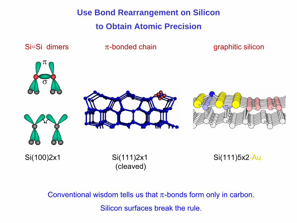
Use Bond Rearrangement on Silicon to Obtain Atomic Precision
Conventional wisdom tells us that -bonds
form only in carbon.
Silicon surfaces break the rule.
Si(100)2x1
Si(111)2x1
Si(111)5x2-Au(cleaved)
Si=Si
dimers
-bonded chain
graphitic silicon

Adatoms
convert three
broken bonds into one.
Holes
eat broken bonds.
Bumps and holes
Si(111)7x7
Most stable silicon surface.
Perfect rearrangement of >100 atoms.

Si(111)7x7 as 2D Template
Aluminum sticks to one of the two 7x7 triangles.
Can put Mn
atoms on top of the aluminum.
Jia
et al.

Straight steps because of the large 7x7 cell.
Wide kinks cost energy.
1 kink in 20 000 atoms
15 nm
Stepped Si(111)7x7as 1D Template

Atomic Perfection by Self-AssemblySmaller is easier (“bottom up”)
One 7x7 cell per terrace
5.731
592
8 nm

Metal atoms that produce 1D
chains on vicinal Si(111) :
I: Li, Na,…
II: Ca, Ba,…
III: In IV: Pb
NM: Ag,
Au TM: Pt RE: Gd, Dy,…
on Si(100):III: BiTM: Ir
on Ge(100):NM: Au TM: Pt

1/3rd-order pattern … was joined by a 1/5th-order pattern
Si(111)5x2-Au structure: found in 1969, still getting refined.

Three Au chains on Si(111)5x2-Au

Au chain
Graphitichoneycomb
chain
Si(557) – Au
Simpler: Single chain

Graphitichoneycomb
chain
Why are these surfaces 1D (not 2D) ?
Perfect lattice match along the chain,
but complete mismatch perpendicular to it
.

Geim
and MacDonald,Physics Today, August 2007
Futuristic molecular switch, made of graphene
ribbons
Maybe silicene
instead?

Graphiticribbon
Si(557)-Au
Single chain of orbitals
The ultimate nanowire
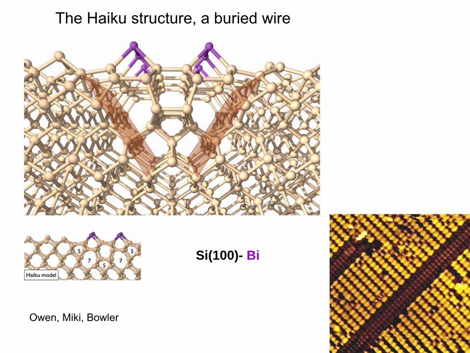
The Haiku structure, a buried wire
Si(100)- Bi
Owen, Miki, Bowler

Physics in One Dimension
• Elegant and simple
• Lowest dimension with translational motion
• Electrons cannot avoid each other
• No such thing as a single electron
• Spinons
and holons
instead
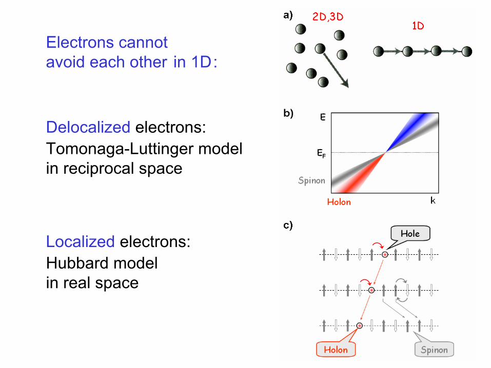
Electrons cannot avoid each other in 1D:
Delocalized electrons:Tomonaga-Luttinger
model
in reciprocal space
Localized electrons:Hubbard modelin real space
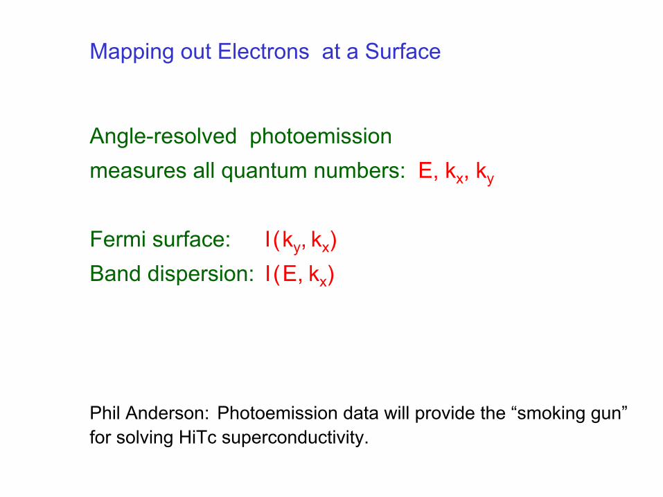
Mapping out Electrons at a Surface
Angle-resolved photoemissionmeasures all quantum numbers:
E, kx
, ky
Fermi surface: I (ky, kx
)Band dispersion:
I (E,
kx
)
Phil Anderson: Photoemission data will provide the “smoking gun”
for solving HiTc
superconductivity.

2D
Fermi Surfaces from 2D to 1D
2D + super-
lattice
1D

Single Chain Double Chain
Si(557)
-Au Si(553) –Au
S = Single Chain Db = Double chain bondingDa = Double chain antibonding
S
A2 A1 A2
E
k
EDb Da
A2 A1 A2
k
E
A2 A1 A2 k
Db S Da
Si(111)
-Au
Three Chains

0 k ZB1x1
EF
Spin-split band similar to that in photoemission
Sanchez-Portal et al. 2004
0
What about the splitting? Prediction: It is magnetic!

Evidence for spin polarization
Spin-polarized, angle-resolved photoemission
Okuda et al. 2010

Non-magnetic Exchange Splitting Rashba SplittingE k
vertical shift horizontal shift“
W”
shape
Various spin splittings
Rashba
(spin-orbit) Hamiltonian:
H
(k
V)
s
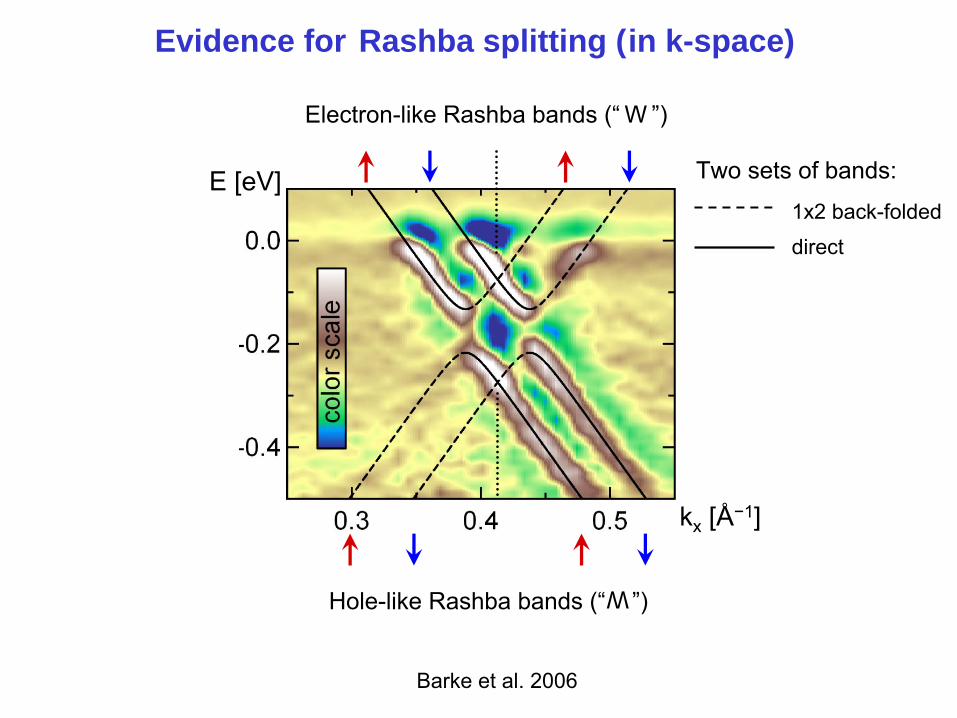
Evidence for Rashba splitting (in k-space)
Barke
et al. 2006
E [eV]
kx
[Å−1]
1x2 back-foldeddirect
Two sets of bands:
Electron-like Rashba
bands (“
W ”)
Hole-like Rashba
bands (“
”)
W

Spin-polarization of broken bonds in real space?
3D: No Spin-paired electrons in -bonds
2D: No Spin-paired electrons in -bonds
1D: ??
0D: Yes Isolated broken bond electron: Pb -center at Si/SiO2 , seen by ESR

GraphiticribbonFocus on the step edge
Look for isolated broken bonds

Si
SiSiSi
Au Au
Au Au
Au Au
Prediction: Magnetism triggers superlattice, couples atoms – electrons – spins
Erwin and Himpsel, Nature Comm. (2010)

Empty minority spin state is the hallmark of the magnetic splitting Eex
Eex
E
EF
Magnetic Non-Magnetic

Calculated magnetic band structure
Two-photon photoemission results
Biedermann
et al., PRB (2012)
A

Two-photon photoemission in k-space
High-resolution technique for unoccupied states. 25 fsec time resolution.
EFermiIR
UV
A
Pho
toel
ectro
n In
tens
ity a
t k |
|=0
A

Snijders
et al., New Journal of Physics (2012)
Scanning tunneling spectroscopy in real space
Spin-polarized edge atoms appear bright. Dangling bond sticks out !
V [V]
dI/dVI/V
D(E)

Wiesendanger, Rev. Mod. Phys. 81, 1495 (2009)
Spin-polarized scanning tunneling spectroscopy
Spin swapped
Large current Small current

Loth
et al., Science 335, 196 (2012)
12 spins/bit, antiferromagnetic,color = spin polarization
Europhysics
News 39, 31 (2008)

Backups

Total filling of 5/3
e- per chain atom
• 5 electrons get distributed over 3 chain atoms (tripling of the unit cell).• Analogous to 1 electron being shared by
3 flux quanta
in the FQHE.
Band Dispersion
Fermi SurfaceFractional Band Filling

Spin-Charge Separation via Tunneling between two Quantum Wires
Auslaender
et al., Science 308, 88 (2005)
Use B-field to transfer momentum: p (p + eA)
E
p

Increase spinon-holon splitting by Coulomb U
TTF-TCNQ
Claessen
et al., PRL 88, 096402 (2002), PRB 68, 125111 (2003)

End atoms disappear at certain bias voltages
Zero-dimensional “surface state” at the end of a one-dimensional chain
Crain and Pierce, Science 307, 703 (2005)
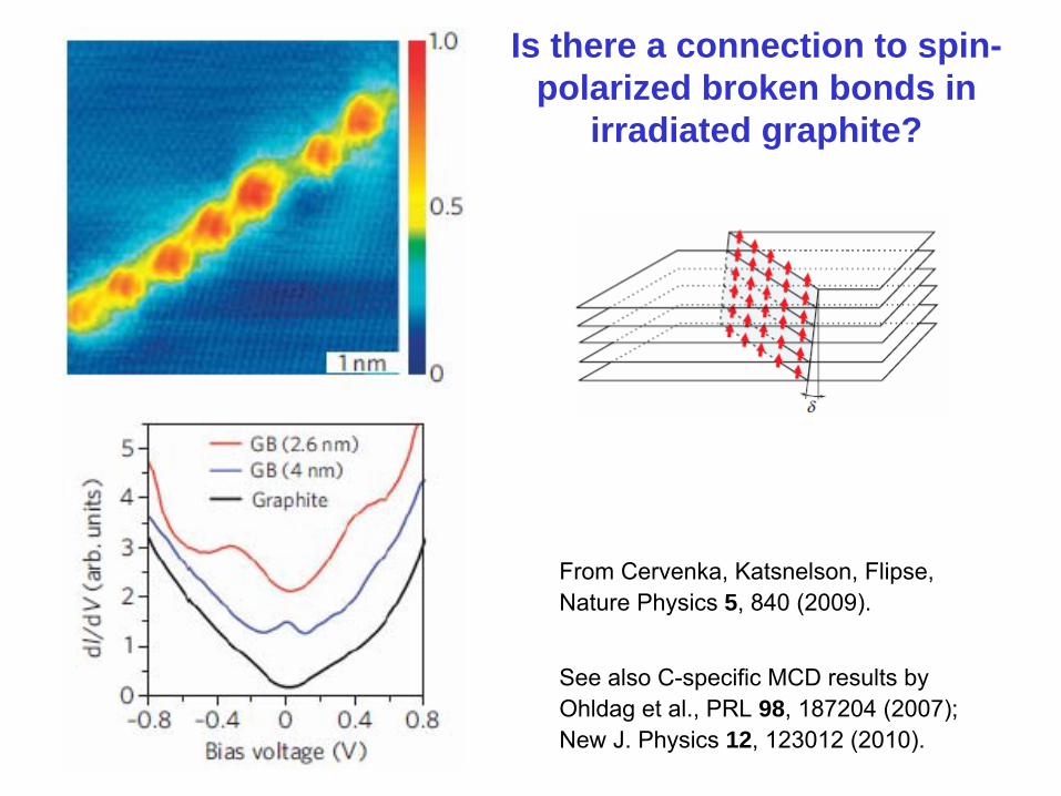
Is there a connection to spin- polarized broken bonds in
irradiated graphite?
See also C-specific MCD results by Ohldag
et al., PRL 98, 187204 (2007); New J. Physics 12, 123012 (2010).
From Cervenka, Katsnelson, Flipse, Nature Physics 5, 840 (2009).

1x3 superlattice formation at the step edge
What are these distortions ?Atoms?
(Reconstruction) Electrons?
(Charge density wave)Magnetic?
(Spin density wave)

Empty StatesTwo-Photon
Photoemission
Rügheimer
et al., PRB 75, 121401(R) (2007)
0 ZB2x1
Predicted step edge band not seen at EF
. Would be rather unstable. How does the surface avoid such high density of states at EF
?
Magnetic splitting shifts minority spin states up
!

Two-photon photoemission processes

Low-lying magnetic states