electronic properties of the residual donor in unintentionally doped...
TRANSCRIPT

Electronic properties of the residual donor in unintentionally doped beta-Ga2O3
Son Tien Nguyen, K. Goto, K. Nomura, Q. T. Thieu, R. Togashi, H. Murakami, Y. Kumagai, A. Kuramata, M. Higashiwaki, A. Koukitu, S. Yamakoshi, Bo Monemar and Erik Janzén
Journal Article
N.B.: When citing this work, cite the original article.
Original Publication:
Son Tien Nguyen, K. Goto, K. Nomura, Q. T. Thieu, R. Togashi, H. Murakami, Y. Kumagai, A. Kuramata, M. Higashiwaki, A. Koukitu, S. Yamakoshi, Bo Monemar and Erik Janzén, Electronic properties of the residual donor in unintentionally doped beta-Ga2O3, Journal of Applied Physics, 2016. 120(23), pp.. http://dx.doi.org/10.1063/1.4972040 Copyright: AIP Publishing
http://www.aip.org/
Postprint available at: Linköping University Electronic Press
http://urn.kb.se/resolve?urn=urn:nbn:se:liu:diva-134498
1
Electronic properties of the residual donor in unintentionally doped β-Ga2O3
N.T. Son1, K. Goto2,3, K. Nomura2, Q. T. Thieu2, R. Togashi2, H. Murakami2, Y. Kumagai2, A. Kuramata3, M. Higashiwaki4, A. Koukitu2, S. Yamakoshi3, B. Monemar1,2 and E. Janzén1 1Department of Physics, Chemistry and Biology, Linköping University, SE-58183 Linköping, Sweden 2Tokyo University of Agriculture and Technology, Koganei, Tokyo 184-8588, Japan 3Tamura Corporation, Sayama, Saitama 350-1328, Japan 4National Institute of Information and Communications Technology, Koganei, Tokyo 184-8795, Japan
Abstract
Electron paramagnetic resonance (EPR) was used to study the donor that is responsible for the
n-type conductivity in unintentionally doped (UID) β-Ga2O3 substrates. We show that in as-
grown material, the donor requires high temperature annealing to be activated. In partly
activated material with the donor concentration in the 1016 cm-3 range or lower, the donor is
found to behave as a negative-U center (often called a DX center) with the negative charge
state DX− lying ~ 16-20 meV below the neutral charge state d0 (or Ed), which is estimated to
be ~ 28-29 meV below the conduction band minimum. This corresponds to a donor activation
energy of Ea ~ 44-49 meV. In fully activated material with the donor spin density close to ~
1×1018 cm-3, donor electrons become delocalized, leading to the formation of impurity bands,
which reduces the donor activation energy to Ea ~15-17 meV. The results clarify the
electronic structure of the dominant donor in UID β-Ga2O3 and explain the large variation in
the previously reported donor activation energy.
PASC number(s): 71.55.Ht, 76.30.Da, 76.30.Pk

2
I. INTRODUCTION
With a very large bandgap (4.8-4.9 eV) and the possibility of high n-type doping, gallium
oxide, β-Ga2O3, is a great transparent conducting material to be used in optical devices
operating in the deep ultraviolet spectral region.1-3 Its material properties are especially suited
for high-voltage and high-power device applications and then even expected to be better than
SiC and GaN.4 The availability of native low-cost substrates is also an advantage of β-Ga2O3
over other wide bandgap semiconductors. The metal-semiconductor field-effect transistors
(MESFETs),4,5 metal-oxide-semiconductor FETs (MOSFETs)6 and Schottky barrier diodes
(SBDs) have recently been demonstrated.5,7,8
Theoretical calculations predicted that substitutional Si, Ge, Sn, F, and Cl impurities
and H (in both substitutional and interstitial sites) have low formation energies and act as
shallow donors in β-Ga2O3.9 Successful n-doping studies have so far been reported for
Sn7,10,11 and Si12,13 where electron densities in the range of 1016-1019 cm–3 can be achieved.
However, little is known on the electronic structure of shallow donors in the material. The
near band-edge photoluminescence (PL) from donor-bound excitons, that can provide detailed
information on the electronic structure of the involved donor in a semiconductor, has so far
not been detected in β-Ga2O3.
Unintentionally doped (UID) β-Ga2O3 substrates can be highly resistive or conductive
with the n-type conductivity. In conductive β-Ga2O3, Binet and co-workers14 observed a
narrow EPR line with slightly anisotropic g-values and attributed it to the resonance of
conduction electrons originating from the O vacancy (VO). Using highly conducting materials
with the unpaired spin concentration of 1018-1019 cm–3 this EPR signal could be detected at
temperatures in the range from 4 K to room temperature.15,16 Mayer and co-workers17
observed that in resistive materials, the EPR signal can only be detected at elevated

3
temperatures with the corresponding concentration being increased with increasing
temperature. They, therefore, assigned this signal to the resonance of conduction electrons and
the broad EPR signal observed at low temperatures in conducting samples to the shallow
donor. Later EPR studies suggested that this donor is related to the O vacancy18 or the Frenkel
pair of VO and the O interstitial, VO-Oi.19 Hall-effect measurements gave an estimated donor
ionization energy in the range of 16-30 meV for conducting β-Ga2O3.20,21 However, hybrid
functional calculations suggested VO to be deep donors and, therefore, cannot be responsible
for the n-type conductivity in UID materials.9 Studies of UID β-Ga2O3 with the conductivity
varying in a large range suggested that the Si impurity in the source material (β-Ga2O3
powder) can account for the observed conductivity.21 The origin of the residual donor in UID
material can have a strong impact on n-type doping of β-Ga2O3, since VO-related donors are
expected to be less thermally stable than substitutional impurity donors and it can be more
difficult to control the conductivity using an intrinsic donor. Understanding the electronic
structure and clarifying the origin of the residual donor in UID β-Ga2O3 is of technological
importance and also of interest from fundamental defect physics.
In this study, we use EPR to study UID β-Ga2O3 substrates before and after high-
temperature annealing for activation of the donor. We show that in partly activated materials
with the spin density in the mid 1016 cm–3 ranges or below, the donor behaves as a negative-U
(or DX) center, similar to the Si donor in high-Al-content AlGaN,22 while in fully activated
samples, donor electrons become delocalized and the transformation from isolated donor
states to corresponding impurity bands occurs, reducing the donor activation energy. In
Section III. A, the DX behaviors and the activation energy of the donor is described. The
delocalization of donor electrons and the decrease of the donor activation energy caused by
the formation of impurity bands are presented in Section III. B, while the origin of the donor
is discussed in Section III. C.

4
II. EXPERIMENTAL DETAILS
The material used in this study is UID β-Ga2O3 (001) substrates grown by the “edge-defined
film-fed growth (EFG)” technique using Ga2O3 powder of 5N grade purity (99.999%) with
the main contaminant being Si. The melted material is pulled by a seed crystal through a
capillary die made of iridium with a growth rate of 15 mm/h. The ambient of the growth
reactor is a mixed gas of nitrogen (98%) and oxygen (2%). Details of the EFG growth are
described elsewhere.23 The typical substrate size is 20 mm × 10 mm × 0.65 mm. The
concentration of different impurities was measured by secondary ion mass spectrometry
(SIMS) at the center and near the edge (8 mm from the center) of the sample and the data for
four impurities with high concentrations or known to act as compensating centers (Fe, Mg) or
donors (Si, Sn) are given in Table I. According to SIMS data, the atomic concentration of Si
is at least one order of magnitude higher than that of other measured impurities. The UID
samples used in this study were cleaved from (001) substrates, close to the edge. Si-doped β-
Ga2O3 (-201) samples with the Si concentration of ~3-4×1018 cm−3, as determined from
capacitance-versus-voltage (CV) measurements, were also used to study the formation of the
impurity band. For partly and fully activation of the donor, the samples were annealed in N2
gas flow at 1000-1110 °C and 1150 °C, respectively.
EPR measurements were performed on an X-band (~9.4 GHz) E500 Bruker
spectrometer equipped with a continuous He-flow cryostat, allowing the regulation of the
sample temperature from 4 K to room temperature. The concentration of the donor at the
neutral charge state or the number of spins was determined from double integration of the
EPR signal and measurement conditions using the spin counting application provided and
calibrated by Bruker. In photo-excitation EPR (photo-EPR) experiments, a 250 W halogen
lamp or a 150 W xenon lamp (for above band gap excitation) were used as excitation sources.
III. RESULTS AND DISCUSSION

5
A. Negative-U behavior of the donor
As-grown UID β-Ga2O3 substrates are of high resistivity judging from the high Q-factors
(~10000 -10200 for a sample with a size of ~10 mm × 2.85 mm × 0.65 mm) at room
temperature. The EPR spectra measured in such a sample at 297 K for the magnetic field B
parallel to the <001> direction in darkness and under illumination of a xenon lamp are shown
in Figs. 1(a) and 1(b), respectively. As can be seen in the figure, only weak EPR signals of the
Fe3+ center and an unidentified line at ~3765 G were observed. No other signals appear at
lower temperatures.
Annealing at below 1000 °C for 10 minutes did not show any change in the Q-factor at
room temperature. After annealing at 1100 °C for 20 minutes, the Q-factor at 293 K was
reduced to ~8800 and a very narrow EPR line with a linewidth of slightly below 0.3 G (the
magnetic field distance between the maximum and minimum of the first derivative EPR line)
appeared [Fig. 1(c)]. From the angular dependence study at room temperature the g-values
were determined as: gxx=1.9606, gyy=1.9577, gzz=1.9630 with the principal gz-axis parallel to
the b-axis of the crystal and the gx-axis is at an angle α~23° from the <001> direction. Within
the experimental errors, the g-tensor of this EPR signal is identical to that of the signal
previously attributed to the resonance of conduction electrons14 and assigned later to the
shallow donor related to VO (gxx=1.960, gyy=1.958, gzz=1.962 and α~24° from the <001>
direction).18 However, the signal can only be detected at elevated temperatures (T>60 K). The
spin density at the donor estimated from EPR at room temperature is ~1×1015 cm–3. In such a
resistive material and a low donor concentration, it is unlikely that the resonance is related to
delocalized electrons.
We have noticed that the Q-factor was hardly improved when the temperature was
lowered to ~50 K when the donor signal has already completely disappeared. This suggests
that the resonance may be not related to conduction electrons, otherwise the Q-factor should

6
increase at low temperatures when the density of conduction electrons is reduced. Mayer and
co-workers17 also reported that in samples with high resistivity, the donor signal could only be
detected at elevated temperatures. They observed that the EPR intensity increases with
increasing temperature and therefore assigned again this donor signal to the resonance of
conduction electrons. However, the linewidth of 2 G at room temperature (~ 9 times larger
than its real linewidth) in their experiments17, indicates a huge line broadening probably due
to using too high field modulations. This will lead to an overestimation of the EPR intensity at
temperature ranges close to room temperature and, hence, an artificial increase of the
estimated donor concentration. (In our experiments, the linewidth is ~ 1 G at 130 K, ~ 0.7 G
at 170 K, ~ 0.4 G at 240 K and ~0.22 G at 297 K.)
EPR spectra in this sample measured at different temperatures are shown in Fig. 2(a).
As can be seen in the figure, the signal gets broader gradually when reducing the temperature
and disappears at temperatures T<60 K. The line broadening was previously attributed to a
superhyperfine interaction between the electron spin and nuclear spins of nearby Ga ions.15,24
We checked the integrated intensity of the signal measured at the same temperature with
different microwave powers (0.1-0.6 mW) and field modulation (0.2-0.7 G) and find out that
using a field modulation larger than 0.4 G at high temperature range will over modulate the
signal, which distorts and broadens the EPR line. In the temperature dependence study, the
field modulation is therefore kept at 0.4 G and the microwave power of ~0.1 mW at high
temperatures in order to avoid signal overloaded, and at ~0.6 mW when measuring at low
temperatures in order to improve the signal-to-noise ratio when the EPR signal becomes
weaker.
The temperature dependence of the donor spin density (or the concentration of donors
in the neutral charge state), n(T), estimated from EPR using the spin-counting application is
shown in Fig. 2(b). The maximum donor concentration in the neutral charge state does not

7
occur at the lowest temperature as expected for a normal shallow donor but appears at an
elevated temperature. Such a temperature dependence of n(T) is typical for a negative-U
donor, often called a DX center, similar to the behavior of the Si donor in high-Al-content
AlGaN.22 In a DX center, the donor in the neutral charge state Ed prefers to capture a second
electron to pair off the spins and undergoes a large lattice relaxation to reduce its energy.25 At
low temperatures, the donors are mainly in the negative charge state DX−, which lies below
Ed and is EPR inactive with the electron spin S=0. Depending on the energy separation
between Ed and DX− (or EDX), the signal can be measured at elevated temperatures when the
thermally induced population on Ed becomes detectable by EPR. With increasing
temperature, the spin density at Ed, n(T), keeps increasing until the temperature is high
enough to excite electrons from Ed to the first effective-mass excited state 2p [see the energy
scheme in the inset of Fig. 2(b)]. Due to competition between these two processes, n(T) will
reach a maximum and then reduces with increasing temperature when the process of
removing electrons from Ed to E2p becomes dominating. With considering only EDX, Ed and
the first effective-mass excited state 2p, the donor spin density n(T) can be described as22
Tk)/ E(ET)/kE(E Bd2pBFd Cee1
Nn(T) −−− ++∝ . (1)
Here N is the total donor concentration, kB is the Boltzmann constant, EF is the Fermi level
with the energy reference at the conduction band minimum (CBM), EC=0, and C is a factor
taking into account the degeneracy of higher-lying excited states within kBT from the 2p state.
From the best fit to n(T) we observed Ed-EF = 10 meV and E2p-Ed = 22 meV. Assuming that
the neutral charge state Ed and excited states of the donor follow the effective mass theory,
i.e. the Ed/i2 rule (i = 1, 2, .., n) or E2p ~ Ed/4 and |E2p – Ed| = |(Ed/4) – Ed| = 3|Ed|/4, we can
estimate |Ed| = 4|E2p-Ed|/3 ~ 29 meV. For a negative-U center, the Fermi level lies at the
middle between the ground state occupied state.26 In the case of a DX donor, EF lies close to
the middle between Ed and EDX levels and |EDX| ~ |Ed| + 2|Ed-EF| ~29 + 20 ~ 49 meV. Thus,

8
in resistive substrates with the donor concentration in the mid 1015 cm–3 range, the activation
energy of the donor is expected to be Ea = EDX ~ 49 meV.
After annealing further the same sample at 1110 °C in N2 gas flow for 180 minutes,
we observe that the Q-factor at 293 K is reduced to ~5400, indicating a more conducting, but
still rather resistive condition. We performed again the temperature dependence study of n(T)
in this sample and the result is shown in Fig. 3. Now the EPR signal can be detected down to
temperatures of ~40 K and we observe a similar temperature dependence of n(T), with its
maximum slightly shifted to lower temperatures. The fit using Eq. (1) gives Ed-EF = 8 meV,
E2p-Ed = 21 meV and, hence, Ed = 28 meV. These values are slightly smaller than that in the
sample before the second annealing at 1110 °C, but the deviations are within the errors of the
method. The donor activation energy is then determined as: Ea = Ed + 2|Ed-EF| = 28 +16 = 44
meV. Thus, with the concentration of low 1016 cm–3 range as estimated by EPR at ~70 K, the
donor also shows clear DX behavior.
Due to different electronic structure, a normal shallow donor and a DX donor can
show different responses to illumination. Under illumination, electrons being trapped at deep
levels, such as the Ga vacancies and other compensated impurities, e.g. Fe and Mg, can be
excited to the neutral charge state d0 via the conduction band. This usually leads to an increase
of the EPR signal of a shallow donor. However, this is not always the case for a DX donor
since electrons on d0 can relax down to the negative charge state DX− if they can get enough
thermal energy to overcome the barrier between the two charge states. The increase of the
donor signal may be observed only at low temperatures, depending on the barrier height. An
example is the Si DX donor in AlN, which shows an enhancement of the EPR signal under
illumination only at temperatures below 60 K.27,28 We performed photo-EPR using both
below and above band gap excitations and found that illumination has no noticeable effect on
the EPR signal of the donor at all studied temperatures. Fig. 4 shows no changes in the

9
intensity of the donor signal measured at 80 K in darkness and under above-band-gap
excitation. At temperatures below 30 K, the donor signal is not observable, neither in darkness
nor under illumination. This suggests that the energy barrier between the neutral and negative
charge states is very low and electrons on the d0 state can relax to the DX− state even at low
temperatures.
B. Delocalized donor electrons and formation of impurity bands
In the sample where the donor has been activated by annealing at 1150 °C, the conductivity is
higher and the coupling of the microwave can be possible only at low temperatures with much
smaller Q-factors (~500-700 at below 60 K). The EPR signal can now be detected down to 4
K, indicating that the Fermi level in this sample locates at Ed or slightly above similar to the
case of an effective mass shallow donor. The donor concentration estimated at 10 K is
~9×1017 cm–3, which is close to the SIMS concentration of Si near the edge of UID substrates
(~7×1017 cm–3). The temperature dependence of n(T) in this sample in the temperature range
below 60 K is shown in Fig. 5.
It is possible that at such a high donor concentration, a slightly overlap of the wave
function between donors may occur and an electron in a DX− state can tunnel to a nearby
ionized donor state, d+, even at low temperatures. Unlike a normal shallow donor, whose
ionized states are available in equilibrium only if compensated deep levels are present in the
material,29 a DX center has an equal number of negatively charged donors and ionized donors.
The tunneling of an electron from a negatively charged donor to a nearby ionized donor is
therefore possible, following the process25: DX− + d+ → 2d0, which creates two neutral
donors. As the result, electrons on DX donors become delocalized and their isolated donor
states transform to impurity bands. This process makes it possible to observe the EPR signal
of the neutral donor at low temperatures. The formation of the d0 band also effectively
reduces the energy required to excite unpaired electrons to the first excited state E2p. The

10
concentration n(T) of the donor in the d0 band follows the thermal distribution as the case of a
shallow effective mass donor30,31
T)/kE(E-T)/kE(E Bd2pBFd Cee5.01
Nn(T)−− ++
∝ . (2)
The best fit of n(T) using Eq. (2) gives Ed-EF = -2 meV and E2p – Ed ~10 meV, which is
about a half of the expected value (21-22 meV) for the case of a single d0 state when the
impurity bands have not been formed. Taking into account the above obtained energy from
the 2p state to the CBM of (EC-E2p) = (E2p – Ed)/3 ~21/3 ~7 meV, the donor activation
energy is expected to be Ea ~10 +7 =17 meV for UID β-Ga2O3 after full activation of the
donor.
The formation of impurity bands with delocalized electrons causes the skin effect,
which hinders the penetration of the microwaves, resulting in the typical asymmetric
Dysonian line shape32,33 of the EPR signal as seen in the case of highly Si-doped GaN.34 In a
normal shallow donor, the negatively charged donor band D− lies above the d0 band, just
below the CBM,29 while in a DX donor as in our case, the highest occupied band is the d0
band. Thus, electrons, that give rise to the observed EPR signal, are still related to the donor
although they can tunnel from a donor to another donor. Therefore, the g-values of the EPR
spectrum should represent the properties of the donor and not electrons in the conduction
band.
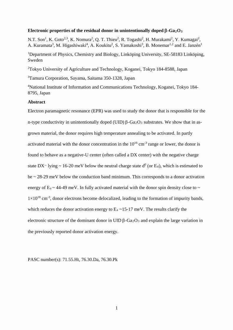
We measured again the angular dependences of the g-value in the partly activated
sample (after annealing at 1110 °C) at two different temperatures: 80 K and 292 K. Their
corresponding g-values versus the angle of the magnetic field in the (010) plane are shown in
Fig. 6(a). The angular dependence measured at 80 K shows the same principal g-values
(except the gyy-component being 0.0002 smaller) and the angles of principal axes and as
compared to that measured at 292 K. These g-values are also the same as the g-values of the

11
donor in the sample annealing at 1100 °C. Figure 6(b) shows the angular dependence of the g-
value in the fully activated sample (after annealing and 1150 °C) measured at 15 K with the
magnetic field rotating from the <010> direction to the <001> direction. The obtained g-
tensor is the same as that in the partly activate sample.
In a previous study18, the g-values were found to be unchanged (within the
experimental errors of ∆g=0.0007) in the temperature range of 5-300 K. Our observed
increase of the g-value with increasing temperature is similar to the observation in Ref. 17.
Such a g-value shift is not expected for a normal shallow donor, whose g-values are usually
decreases with increasing temperature. The g-value shift in this case mainly occurs for the gyy
and gzz components, i.e. the g-value at the direction close to the normal of the cleavage plane
(100) and in the <010> direction of the b-axis. It is possible that this shift of the g-value with
temperature is related to the changes in the local environment of the donor induced by the
anisotropic thermal expansion of the crystal with increasing temperature, which was observed
in the study of the lattice expansion by Víllora and co-workers.35 Thus, all the EPR studies so
far show that the donor in either resistive or highly conducting β-Ga2O3 has the same
anisotropic g-tensor. The anisotropic g-values in the range 1.958-1.963 are typical for a
shallow donor. Delocalized electrons in the D− band of a normal shallow donor, which lies
just below the conduction band, are actually free electrons in the conduction band. Binet and
co-workers14 suggested that the anisotropy of the g-values of the resonance of conduction
electrons is caused by the anisotropy of the conduction band structure of β-Ga2O3. In the
frame of the DX model, both the delocalization of electrons and the anisotropy of the g-value
can be well explained since the delocalized electrons are confined in the d0 band, not in the
conduction band.
In the UID sample annealed at 1150 °C with a donor activation energy Ea ~ 17 meV,
the EPR line is symmetric, showing no Dysonian line shape (see the inset of Fig. 5). This

12
means that the delocalization of electrons may occur locally and the conductivity is not high
enough to induce the skin effect that causes the asymmetric resonance line shape.32,33 In
another UID sample with a slightly higher donor concentration (~1.5×1018 cm–3 as estimated
by EPR), the transition from a normal line shape to the Dysonian line shape can be detected in
the temperature range ~20-30 K [see Fig. 7(a)]. As can be seen in the figure, the EPR line
measured at 20 K is symmetric with equal amplitude of the positive and negative parts of the
line (A/B ~1). At ~30 K and higher temperatures, this ratio increases to A/B~ 1.8-1.9 and the
line shows a clear Dysonian shape. A similar transition from Lorentzian to Dysonian line
shape was also seen in the study by Mayer and co-workers at the temperature range 50-100 K
[see Fig. 2(b) in Ref. 17]. In an intentionally Si-doped substrate with the donor concentration
of ~3-4×1018 cm–3, the Dysonian line shape is already observed at 6.5 K [see Fig. 7(b)]. The
ratio A/B ~ 1.9 is smaller than that of conduction electrons (the A/B ratio varies between 2.7
and 19),32,33 suggesting that the level of electron delocalization in our study is moderate.
The linewidth narrowing with increasing temperature was previously observed and
explained as due to quenching of the hyperfine interaction between the donor electron spin
and the nuclear spins of surrounding nuclei caused by the motion of delocalized electrons
between donor sites.15,17,24 The linewidth narrowing observed in our partly activated, high-
resistance samples [see Fig. 2(a)] cannot be due to the motion of delocalized electrons, but
may be mainly caused by the enhancement of the average lifetime of electrons on the neutral
charge state with increasing temperature since d0 is actually the excited state, not the ground
state of this DX donor. The linewidth narrowing with increasing temperature due to the
motion of delocalized electrons is expected in high conducting samples as can be seen in Figs.
7(a) and 7(b). In addition to the effect of temperature, linewidth narrowing is also enhanced
with increasing the concentration of delocalized electrons. In the UID sample with the donor
concentration of ~1.5×1018 cm–3, the linewidth at 20 K is ~3 G [Fig. 7(a)], while in the sample

13
doped with Si to a concentration of ~3-4×1018 cm–3, the linewidth is only ~1.1 G at 18.5 K
and ~1.5 G at 6.5 K.
The temperature dependence of n(T) in the UID sample with the donor concentration
~1.5×1018 cm–3 is shown in Fig. 8. The best fit using Eq. (2) gives Ed-EF = -2 meV and E2p-
Ed = 8 meV. This energy threshold is close to the value of 7.5 meV reported by Mayer and
co-workers17 in conducting β-Ga2O3 and of ~7 meV reported by Víllora et al35 in UID β-
Ga2O3 samples grown by floating zone technique using less pure source materials (99.99%)
with the carrier concentration in the low 1018 cm−3 range. Adding the energy distance EC-E2p
~ 7 meV, the donor activation energy is expected to be Ea ~ 15 meV for β-Ga2O3 with the
donor concentration in the low 1018 cm–3 range.
C. Origin of the donor
Recent ab initio calculations9 suggest that VO is a deep donor with the (2+|0) level located at
more than 1 eV below the CBM, and for all Fermi levels positions, +OV can be observable by
EPR only under illumination. The VO center in ZnO also shows similar properties, i.e. being a
deep donor with +OV only detectable by EPR under illumination.36,37 The donor in UID β-
Ga2O3, with an activation energy being much smaller than that predicted for VO and with its
signal detectable in darkness, is unlikely to be related to the O vacancy. In a recent EPR
study, Yamaga and co-workers19 noticed that in β-Ga2O3 doped with Si, Zr, and Hf, an EPR
line with the same g-values was observed. They suggested a defect model, in which the excess
electron from the substitutional impurity being trapped at the O vacancy-O interstitial Frenkel
pair, VO-Oi, to explain the EPR observation. However, our annealing studies show that the
donor is very thermally stable and may not be explained by the model of the VO-Oi Frenkel
pair, which is expected to be dissociated at high temperatures. It is known that Si substituting
for Ga and O at the N site are shallow donors in GaN and their EPR spectra are not

14
distinguishable in the g-values. Therefore, it is possible that Si, Sn, Zr and Hf donors in β-
Ga2O3 give rise to EPR signals with similar g-values.
The donor in UID β-Ga2O3 was previously suggested to be related to Si based on its
presence in the source material with the concentration similar to the free carrier concentration
determined from Hall-effect measurements21 or from the Si-doping studies.12,13 A recent study
also shows that the free carriers activated by annealing in N2 gas are similar to the doped Si
concentration.23 In Si-doped β-Ga2O3 to a concentration of 1×1019 cm–3, the free carrier
concentration was found to increase sharply with annealing at 800-1000 °C and reaches an
electrically activated level of more than 80%.12 In Si-doping of β-Ga2O3 epitaxial layers
grown by halide vapor phase epitaxy, a controlled n-type conductivity with the carrier
concentration from 1015 to 1018 cm−3 could be achieved and post annealing in N2 gas at ~1000
°C for activation of the Si donor is a part of the doping procedure.38 A recent study of Si-
doping in β-Ga2O3 epitaxial layers grown by metal organic vapor phase epitaxy reported that
with the Si concentration up to 4×1018 cm–3, the layer is still semi-insulating after annealing at
800-850 °C in O2 gas for one hour.39 Kuramata and co-workers23 also showed that in the same
set of β-Ga2O3 samples doped with Si to the concentration in the range of 1018-1019 cm–3,
annealing in O2 gas at 1150 °C did not activate the donors, but annealing at 800-1000 °C in
N2 gas gave rise to the free carrier concentration in the same Si doping range. While it is still
unclear why annealing in O2 prevents Si-doped β-Ga2O3 becoming conductive, the reported
doping studies all suggest that Si is the source of free electrons.
At room temperature, with the DX− state lying only ~16-20 meV below the neutral
state of the effective mass donor, Si will provide free electrons as a shallow donor. As shown
from SIMS, Si is the dominant impurity with the concentration comparable to the donor
concentration estimated by EPR. Thus, Si should have the dominant contribution to the EPR
signal of the donor in UID and activated β-Ga2O3. Considering the requirement of high

15
temperature annealing for donor activation and the fair correlation between the concentration
of donor determined by EPR and the concentration of Si obtained from SIMS, Si appears to
be the best candidate for the donor that is responsible for the residual n-type conductivity in
UID β-Ga2O3. The requirement of high-temperature annealing for donor activation may
suggest that Si after the growth is passivated by other impurities or intrinsic defects, similar to
the case of Mg acceptors in GaN.40 Unfortunately, the DX structure with the neutral state d0
lying above the ground state DX− makes it impossible to saturate the EPR transition even
using the maximum available microwave power of 200 mW. Therefore, electron nuclear
double resonance experiments cannot be performed for chemical identification of the donor.
IV. SUMMARY
In summary, using EPR we study UID β-Ga2O3 substrates before and after annealing in N2
gas ambient for activation of the donor at different levels corresponding to different donor
concentrations and conductivities. We show that as-grown material is highly resistive,
showing no EPR signal of the donor. After annealing at ~1100-1110 °C the donor is partly
activated with the donor spin density in the range of mid 1015- low 1016 cm–3 and shown to
behaves as a negative-U center with the negative charge state DX− locating at ~16-20 meV
below the neutral charge state Ed, which lies at ~28-29 meV below the CBM. The
corresponding donor activation energy is estimated to be Ea~44-49 meV. After annealing at
1150 °C, the donor is fully activated with the concentration ~ 9×1017 cm–3 and donor electrons
become partly delocalized, forming impurity bands, which reduces the donor activation
energy to Ea ~17 meV. In UID samples with the donor concentration reaching ~1×1018 cm–3
or in Si-doped samples with the concentration of ~3-4×1018 cm–3, the EPR signal shows a
clear Dysonian line shape, which is typical for the resonance of delocalized electrons, and a
donor activation energy of ~ 15 meV is determined. The DX properties of the donor and the
formation of impurity bands explain the large variation of the donor activation energies

16
previously reported by transport measurements. Based on the correlation between the donor
concentration estimated by EPR and the Si concentration determined by SIMS as well as their
annealing behaviors, the donor responsible for the n-type conductivity in UID β-Ga2O3 is
assigned to Si. Due to a small energy distance between the DX− state and the neutral state d0
of ~20 meV, Si will behave as a shallow donor at the operating temperature of devices.
Acknowledgments
Support from the Linköping Linnaeus Initiative for Novel Functional Materials (LiLi-NFM),
the Council for Science, Technology and Innovation (CSTI), Cross-ministerial Strategic
Innovation Promotion Program (SIP), “Next-generation power electronics” (funding agency:
NEDO, Japan) is acknowledged.
References 1K. Shimamura, E. G. Víllora, K. Domen, K. Yui, K. Aoki, and N. Ichinose, Jpn. J. Appl. Phys. 44, L7 (2005). 2Y. Kokubun, K. Miura, F. Endo, and S. Nakagomi, Appl. Phys. Lett. 90, 031912 (2007). 3T. Oshima, T. Okuno, N. Arai, N. Suzuki, S. Ohira, and S. Fujita, Appl. Phys. Express 1, 011202 (2008). 4M. Higashiwaki, K. Sasaki, A. Kuramata, T. Masui, and S. Yamakoshi, Appl. Phys. Lett. 100, 013504 (2012). 5M. Higashiwaki, K. Sasaki, A. Kuramata, T. Masui, and S. Yamakoshi, Phys. Status Solidi A 211, 21 (2014). 6M. Higashiwaki, K. Sasaki, T. Kamimura, M. H. Wong, D. Krishnamurthy, A. Kuramata, T. Masui, and S. Yamakoshi, Appl. Phys. Lett. 103, 123511 (2013). 7K. Sasaki, A. Kuramata, T. Masui, E. G. Víllora, K. Shimamura, and S. Yamakoshi, Appl. Phys. Express 5, 035502 (2012). 8H. Murakami, K. Nomura, K. Goto, K. Sasaki, K. Kawara, Q. T. Thieu, R. Togashi, Y. Kumagai, M. Higashiwaki, A. Kuramata, S. Yamakoshi, B. Monemar, and A. Koukitu, Appl. Phys. Express 8, 015503 (2015). 9J. B. Varley, J. R. Weber, A. Janotti, and C. G. Van de Walle, Appl. Phys. Lett. 97, 142106 (2010). 10N. Ueda, H. Hosono, R. Waseda, and H. Kawazoe, Appl. Phys. Lett. 70, 3561 (1997). 11N. Suzuki, S. Ohira, M. Tanaka, T. Sugawara, K. Nakajima, and T. Shishido, Phys. Status

17
Solidi C 4, 2310 (2007). 12E. G. Víllora, K. Shimamura, Y. Yoshikawa, T. Ujiie, and K. Aoki, Appl. Phys. Lett. 92, 202120 (2008). 13K. Sasaki, M. Higashiwaki, A. Kuramata, T. Masui, and S. Yamakoshi, Appl. Phys. Express 6, 086502 (2013). 14L. Binet, D. Gourier and C. Minot, Journal of Solid State Chemistry 113, 420 (1994). 15E. Aubay and D. Gourier, Phys. Rev. B 47, 15023 (1993). 16D. Gourier, E. Aubay and J. Guglielmi, Phys. Rev. B 50, 2941 (1994). 17B. K. Meyer, U. Leib, A. Hofstaetter, C. Krummel, and D. Kohl, Mater. Sci. Forum 258-263, 1473 (1997). 18M. Yamaga, E.G. Villora, K. Shimamura, N. Ichinose, M. Honda, Phys. Rev. B 68, 155207 (2003). 19M. Yamaga, H. Tsuzuki, S. Takano, E. G. Villora, K. Shimamura, J. Non-Cryst. Solids 358, 2458 (2012). 20M.R. Lorenz, J.F. Woods and R.J. Gambino, J. Phys. Chem. Solids 28, 403 (1967). 21K. Irmscher, Z. Galazka, M. Pietsch, R. Uecker, and R. Fornari, J. Appl. Phys. 110, 063720 (2011). 22X.T. Trinh, D. Nilsson, I.G. Ivanov, E. Janzén, A. Kakanakova-Georgieva, and N.T. Son, Appl. Phys. Lett. 105, 162106 (2014). 23A. Kuramata, K. Koshi , S. Watanabe, Yu Yamaoka, T. Masui, and S. Yamakoshi, J. J. Appl. Phys. 55, 1202A2 (2016). 24L. Binet and D. Gourier, J. Phys. Chem. Solids 59, 1241 (1998). 25D. J. Chadi and K. J. Chang, Phys. Rev. Lett. 61, 873 (1988). Phys. Rev. B 39, 10 063 (1989). 26D. Adler and E. J. Yoffa, Phys. Rev. Lett 36, 1197 (1976). 27M. W. Bayerl, M. S. Brandt, T. Graf, O. Ambacher, J. A. Majewski, M. Stutzmann, D. J. As, and K. Lischka, Phys. Rev. B 63, 165204 (2001). 28N. T. Son, M. Bickermann, and E. Janzén, Appl. Phys. Lett. 98, 092104 (2011). 29B.I. Shklovskii and A.L. Efros, in Electronic properties of doped semiconductors (Springer-Verlag Berlin Heidelberg 1984), p. 52. 30N.W. Ashcroft and N.D. Mermin, Solid State Physics (Books/Cole, Bermont, 1976), p. 581. 31N.T. Son, Y.-S. Kim, and E. Janzén, Phys. Status Solidi RRL 9, 707 (2015), Supporting Information.

18
32G. Feher and A.F. Kip, Phys. Rev. 98, 337 (1955). 33F.J. Dyson, Phys. Rev. 98, 349 (1955). 34A. Wolos, Z. Wilamowski, M. Piersa, W. Strupinski, B. Lucznik, I. Grzegory, and S. Porowski, Phys. Rev. B 83, 165206 (2011). 35E.G. Víllora, K. Shimamura, T. Ujiie, and K. Aoki, Appl. Phys. Lett. 92, 202118 (2008). 36J. M. Smith, V.H. Vehse, Phys. Lett. A 31, 147 (1970). 37C. Gonzales, D. Galland, and A. Hervé, Phys. Stat. Sol. (b) 72, 309 (1975). 38K. Goto, K. Nomura, H. Murakami, Q. T. Thieu, R. Togashi, Y. Kumagai, A. Kuramata, B. Monemar, A. Koukitu, and S. Yamakoshi, Abstract G4, International Workshop on Gallium Oxide and Related Materials, Kyoto, 2015. 39D. Gogova, G. Wagner, M. Baldini, M. Schmidbauer, K. Irmscher, R. Schewski, Z. Galazka, M. Albrecht, and R. Fornari, J. Crys. Growth 401, 665 (2014). 40S. Nakamura, T. Mukai, M. Senoh and N. Iwasa, J. J. Appl. Phys. 31, L139 (1992).

19
Table I: Concentration, given in the unit of 1017 cm−3, of Si, Sn, Fe and Mg measured by SIMS at the center and near the edge (~8 mm from the center) of the UID β-Ga2O3 substrate with the size of 10 mm × 20 mm,. The samples used in this study are cleaved from the region closed to the edge of the substrate.
Position Si Fe Sn Mg Center Edge
1.1 7.1
0.1 0.4
0.05 0.2
0.03 0.8

20
FIG1: (Color online) EPR spectra measured in an as-grown UID β-Ga2O3 substrate for
B||<001> (a) in darkness, and (b) under illumination by a xenon lamp, showing only weak
signals of Fe3+ and an unidentified center (the line at the magnetic field ~3765 G). (c) EPR
spectrum in the same sample after annealing at 1100 °C in N2 gas flow for 20 minutes
measured in darkness showing a narrow signal of the shallow donor.

21
FIG. 2: (Color online) (a) EPR spectra of the residual shallow donor measured for B||[001] at
different temperatures in an UID β-Ga2O3 substrate annealed at 1100 °C in N2 gas flow for
20 minutes to partly activate the donor. All the spectra were measured with a field modulation
of 0.4 G and a microwave power of 0.6325 mW. (b) The temperature dependence of the
concentration of the donor in the neutral charge state determined from EPR. The solid curve
represents the fit to the experimental data using Eq. (1). The inset shows the energy level
scheme of a DX center.

22
FIG. 3: (Color online) Temperature dependence of the concentration of the donor in the
neutral charge state in the β-Ga2O3 sample mentioned in Fig. 2 after another anneal at 1110
°C for 180 minutes to further activate the residual donor. The solid curve represents the fit to
the experimental data using Eq. (1).
FIG. 4: (Color online) EPR spectra of the donor in the β-Ga2O3 sample mentioned in Fig. 3
measured for B⊥<001> (along the a-axis) at 80 K in darkness (thick grey line) and under
illumination by a xenon lamp (thin red line), showing no effect of illumination on the donor
signal.

23
FIG. 5: (Color online) Temperature dependence of the unpaired spin density in an UID β-
Ga2O3 sample fully activated of the residual donor by annealing at 1150 °C in N2 gas flow.
The solid curve represents the fit to the experimental data using Eq. (2). The inset shows the
EPR spectrum of the donor with a symmetric line shape.
24
FIG. 6: (Color online) Angular dependence of the g-value of the donor spectra in UID β-
Ga2O3: (a) in the sample after annealing at and 1110 °C measured at 80 K (o) and at 292 K
(∆) with the magnetic field B rotating in the (010) plane; and (b) in a fully activated sample
after annealing and 1150 °C measured at 15 K with B rotating from the <010> direction to the
<001> direction. The solid curves represent the fitting of the experimental data. The inset in
(a) shows narrow (~0.22 G) and broad (~3.7 G) EPR lines measured at 292 K and 80 K,
respectively.

25
FIG. 7: (Color online) (a) EPR spectra in an UID, fully activated β-Ga2O3 sample with a spin
density of ~1.5×1018 cm−3 showing the transition from Lorentzian line shape to Dysonian line
shape caused by delocalized electrons at ~30 K. (b) In a (-201) Si-doped β-Ga2O3 sample
with a higher donor concentration of ~3-4×1018 cm−3, the Dysonian line shape is already
observed at 6.5 K. With the same magnetic field scale of 52 G in both (a) and (b), the
linewidth of these spectra can be compared with each other directly.

26
FIG. 8: (Color online) Temperature dependence of the unpaired spin density in the UID β-
Ga2O3 sample mentioned in Fig. 7(a). The solid curve represents the fit to the experimental
data using Eq. (2).