electronic devices and circuits ppt_0.pdf · electronic devices and circuits prepared by: mr. v....
TRANSCRIPT

ELECTRONIC DEVICES AND CIRCUITS
Prepared By: Mr. V. R.Seshagiri Rao,Professor Mr. M. Ramesh Babu, Professor, Mr. D. Khalandar Basha, Associate Professor, Ms. C. Deepthi, Associate Professor

Unit-1 PN Junction Diode & Special Function
Electronic Devices

Atomic Structure
An atom is composed of : • Nucleus ( which contains positively charged protons
and neutral neutrons)
• Electrons (which are négative charged and that orbit
the nucleus)

Valence Electrons
• Electrons are distributed in various shells at different distances from nucleus • Electron energy increases as shell radius increases. • Electrons in the outer most Shell are called as valence electrons • Elements in the period table are grouped according to the number of valence electrons.

Valence Electrons
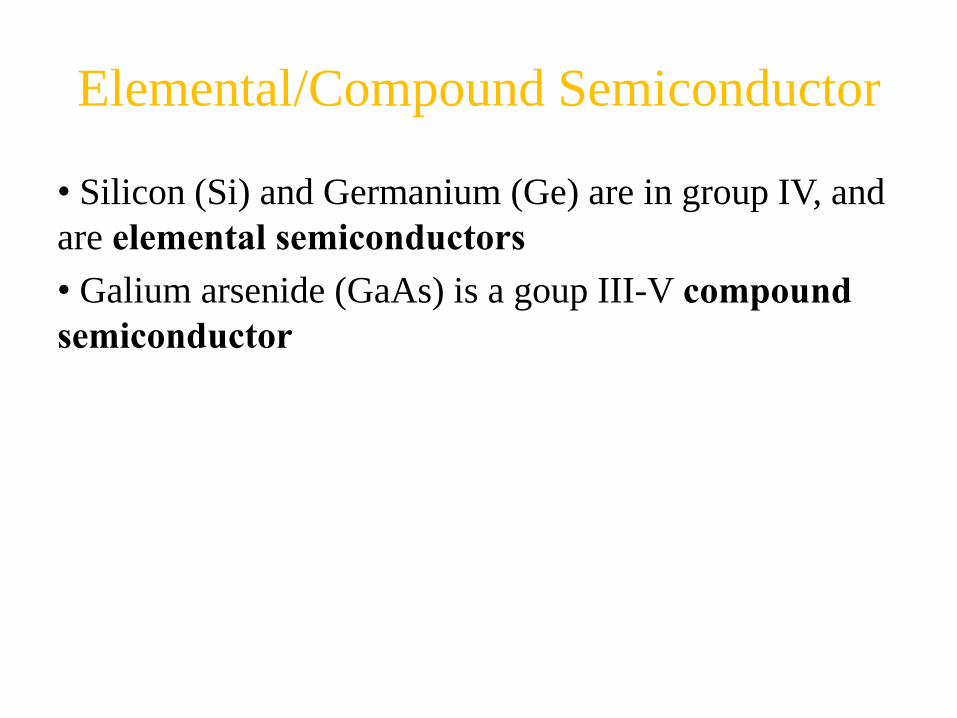
Elemental/Compound Semiconductor
• Silicon (Si) and Germanium (Ge) are in group IV, and
are elemental semiconductors
• Galium arsenide (GaAs) is a goup III-V compound
semiconductor

Silicon Crystal
• → At 0°K, each electron is in its lowest possible energy state, and each covalent bounding position is
filled.
• →If a small electric field is applied, the electrons will
not move → silicon is an insulator

Silicon Atom Diagram at 0°K

Intrinsic Silicon
• → If the temperature increases, the valence electrons
will gain some thermal energy, and breaks free from the covalent bond → It leaves a positively charged
hole
• → In order to break from the covalent bond, a valence electron must gain a minimun energy Eg:
Bandgap energy

Silicon Atom Diagram at Ambiant Temp

Insulators/Conductors
• Materials that have large bandgap energies (in the
range of 3 to 6 electron-volts (eV)) are insulators,
because at room temperature, essentially no free
electron exists in the material • Materials that contain very large number of free
electrons at room temperature are conductors

Semiconductors
• → In a semiconductor, the bandgap energy is in the
order of 1 eV. The net flow of free electrons causes a
current. • → In a semiconductor, two types of charged particles
contribute to the current: the negatively charged
electrons and the positively charged holes

Movement of Holes Movement of Holes

Semiconductor Constants
• The concentration of electrons and holes directly
influence the magnitde of the current
• In an intrinsic semiconductor (a single crystal semiconductor) the densities of holes and electrons
are equal.

ni: intrinsic carrier concentration for free
electrons (same for holes)
B: constant related to specific semiconductor material Eg: Bandgap energy (eV) T: Temperature (°K) K: Boltzman Constant (86 E-06 eV/°K)

Semiconductor Constants

Extrinsic Semiconductor / Doping
• The electron or hole concentration can be greatly
increased by adding controlled amounts of certain
impurities • For silicon, it is desirable to use impurities from the
group III and V.
• An N-type semiconductor can be created by adding
phosphorus or arsenic

Extrinsic Semiconductor / Doping
• The phosphorus (group V) atom is called donor impurity because it donates an electron that is free to
move
• The boron (group III) has accepted a valence electron
(or donated a hole), it is therefore called acceptor
impurity

N-Type Semiconductor

P-Type Semiconductor

Introduction to Semiconductor Devices Semiconductor p-n junction diodes

p-n junction formation
p-type material
Semiconductor material
doped with acceptors.
Material has high hole concentration Concentration of free electrons in p-type material is very low.
n-type material
Semiconductor material
doped with donors.
Material has high concentration of free
electrons.
Concentration of holes in
n-type material is very low.

p-n junction formation
p-type material
Contains
NEGATIVELY
charged acceptors
(immovable) and
POSITIVELY charged
holes (free).
Total charge = 0
n-type material
Contains POSITIVELY
charged donors
(immovable) and
NEGATIVELY
charged free electrons.
Total charge = 0

Diffusion
A substance, the purple dots, in
solution. A membrane prevents
movement of the water and the
molecules from crossing from
one side of the beaker to the other.
Now that the gates have been
opened, the random movements of
the molecules have caused, overtime, the number of molecules to be equal on the two sides of the barrier.

Diffusion
As a result of diffusion, the molecules or other free
particles distribute uniformly over the entire volume

p- n junction formation
What happens if n- and p-type materials are in close contact?
Being free particles, electrons start diffusing from n-type material into p-material
Being free particles, holes, too, start diffusing from p-type material into n-material
Have they been NEUTRAL particles, eventually all the free electrons
and holes had uniformly distributed over the entire compound crystal.
However, every electrons transfers a negative charge (-q) onto the p- side and also leaves an uncompensated (+q) charge of the donor on the n-side. Every hole creates one positive charge (q) on the n-side and (-q) on the p-side

p- n junction formation What happens if n- and p-type materials are in close contact?
p-type
n-type
Electrons and holes remain staying close to the p-n junction because negative and positive charges attract each other. Negative charge stops electrons from further diffusion
Positive charge stops holes from further diffusion
The diffusion forms a dipole charge layer at the p-n junction interface.
There is a “built-in” VOLTAGE at the p-n junction interface that prevents
penetration of electrons into the p-side and holes into the n-side.

p- n junction current - voltage characteristics
What happens when the voltage is applied to a p-n junction?
p-type
n-type
The polarity shown, attracts holes to the left and electrons to the right.
According to the current continuity law, the current can only flow if all
the charged particles move forming a closed loop
However, there are very few holes in n-type material and there are very few electrons in the p-type material. There are very few carriers available to support the current through the junction plane For the voltage polarity shown, the current is nearly zero

p- n junction current - voltage characteristics
What happens if voltage of opposite polarity is applied to a p-n junction?
p-type
n-type
The polarity shown, attracts electrons to the left and holes to the right.
There are plenty of electrons in the n-type material and plenty of holes in
the p-type material.
There are a lot of carriers available to cross the junction. When the voltage applied is lower than the built-in voltage,
the current is still nearly zero When the voltage exceeds the built-in voltage, the current can flow through
the p-n junction

Diode current - voltage (I-V) characteristics
Semiconductor diode consists of a p-n junction with two contacts attached to the p- and n- sides
p
n V
0
qV
I
I
S
exp
1
kT
IS is usually a very small current, IS ≈ 10-17 …10-13 A
When the voltage V is negative (“reverse” polarity) the exponential term ≈ -1;
The diode current is ≈ IS ( very small).
When the voltage V is positive (“forward” polarity) the exponential term
increases rapidly with V and the current is high.

Graphing the I-V characteristics of electronic components.
The I-V plot represents is the dependence of the current I through the component on the voltage V across it.
1
Resistor
V I R; I
I
I = V / R;
R = V/I
R
a DI
DV
V R
tg(a) = 1/R
V
The I-V characteristic of the resistor

The I-V characteristic of the diode
I I
S
qV
exp
1
kT
IS

The experimental I-V characteristic of a Si

p- n diode circuit notation
When “plus” is applied to the p-side,
the current is high. This voltage
polarity is called FORWARD. When “plus” is applied to the n-side,
I
I ex
S
IS
the current is nearly zero. This voltage
polarity is called REVERSE.

p- n diode applications
Light emitters
+
-
p-type
P-n junction can emit the light when forward biased
n-type
Electrons drift into p-material and find plenty of holes there. They “RECOMBINE” by filling up the “empty” positions. Holes drift into n-material and find plenty of electrons there. They also “RECOMBINE” by filling up the “empty” positions. The energy released in the process of “annihilation” produces PHOTONS - the particles of light
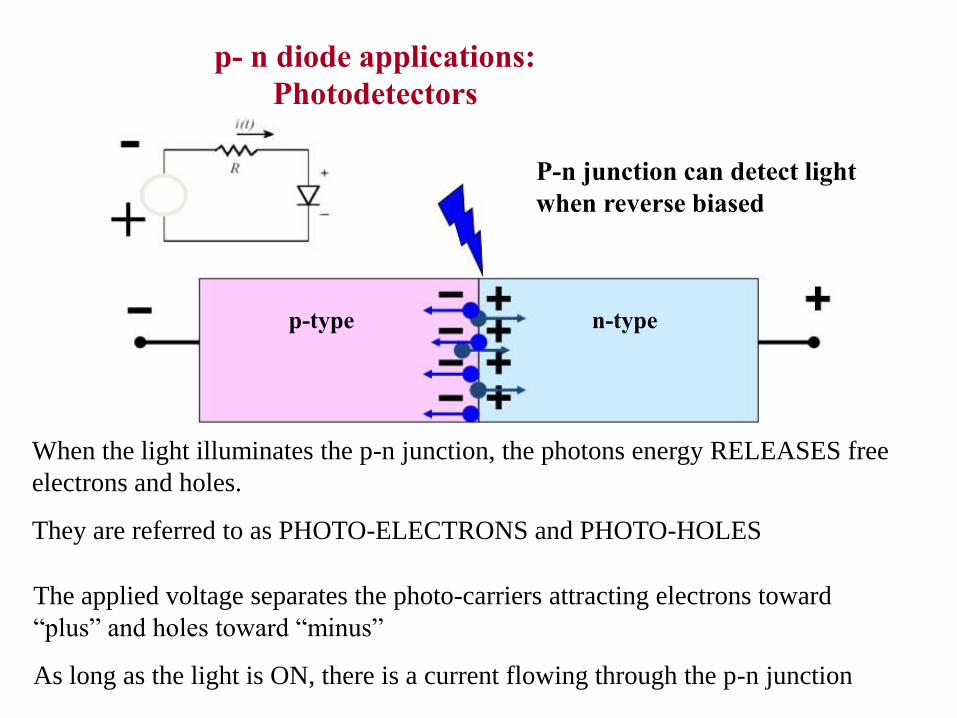
p- n diode applications:
Photodetectors
P-n junction can detect light when reverse biased
p-type
n-type
When the light illuminates the p-n junction, the photons energy RELEASES free electrons and holes. They are referred to as PHOTO-ELECTRONS and PHOTO-HOLES
The applied voltage separates the photo-carriers attracting electrons toward “plus” and holes toward “minus” As long as the light is ON, there is a current flowing through the p-n junction

NEGATIVE RESISTANCE DEVICE
• It is a device which exhibits a negative incremental resistance over a limited range of V-I characteristic. • It is of two types :- 1. Current controllable type : V-I curve is a
multi valued function of voltage and single valued function of current .eg:- UJT, p-n-p-n diode 2. Voltage controllable type : V-I curve is a
multi valued function of current and single valued function of voltage. eg:- SCS, Tunnel diode
-

TUNNEL DIODE (Esaki Diode)
• It was introduced by Leo Esaki in 1958. • Heavily-doped p-n junction
EV
- Impurity concentration is 1 part in 10^3 as compared to 1
part in 10^8 in p-n junction diode
• Width of the depletion layer is very small
(about 100 A).
• It is generally made up of Ge and GaAs. • It shows tunneling phenomenon. • Circuit symbol of tunnel diode is :

WHAT IS TUNNELING • Classically, carrier must have energy at least equal to
potential-barrier height to cross the junction .
• But according to Quantum mechanics there is finite probability that it can penetrate through the barrier for a
thin width.
• This phenomenon is
called tunneling and
hence the Esaki Diode
is know as Tunnel Diode.

CHARACTERISTIC OF TUNNEL DIODE
Ip
Ip:- Peak Current
Iv :- Valley Current
Vp:- Peak Voltage - Ve Resistance Region
Vv:- Valley Voltage
Vf:- Peak Forward
Voltage
Reverse voltage
Iv
Vp Vv Vf Forward Voltage

ENERGY BAND DIAGRAM
Energy-band diagram of pn junction in thermal equilibrium in which both the n and p region are degenerately doped.

AT ZERO BIAS
Simplified energy-band diagram and I-V characteristics of the tunnel diode at zero bias. -Zero current on the I-V diagram;
-All energy states are filled below EF on both sides of the junction;

AT SMALL FORWARD VOLTAGE
Simplified energy-band diagram and I-V characteristics of the tunnel diode at a slight forward bias. -Electrons in the conduction band of the n region are directly opposite to
the empty states in the valence band of the p region.
-So a finite probability that some electrons tunnel directly into the empty
states resulting in forward-bias tunneling current.

AT MAXIMUM TUNNELING CURENT
Simplified energy-band diagraam and I-V characteristics of the tunnel diode at a forward bias
producing maximum tunneling current.
-The maximum number of electrons in the n region are opposite to the
maximum number of empty states in the p region.
- Hence tunneling current is maximum.

AT DECREASING CURRENT REGION
Simplified energy-band diagram and I-V characteristics of the tunnel diode at a higher forward
bias producing less tunneling current.
-The forward-bias voltage increases so the number of electrons on the n side,
directly opposite empty states on the p side decreases.
- Hence the tunneling current decreases.

AT HIGHER FORWARD VOLTAGE
Simplified energy-band diagram and I-V characteristics of the tunnel diode at a forward bias for which the diffusion current dominates.
-No electrons on the n side are directly opposite to the empty
states on the p side.
- The tunneling current is zero. -The normal ideal diffusion current exists in the device.

AT REVERSE BIAS VOLTAGE
- Electrons in the valence band on the p side are directly opposite to
empty states in the conduction band on the n side.
-Electrons tunnel directly from the p region into the n region.
- The reverse-bias current increases monotonically and rapidly with
reverse-bias voltage.

TUNNEL DIODE EQUIVALENT CIRCUIT •This is the equivalent circuit of tunnel diode when biased in negative
resistance region. •At higher frequencies the
series R and L can be ignored.
rs
Cj -R
Ls
•Hence equivalent circuit can be reduced to parallel
combination of junction capacitance and negative
resistance.

Zener Diode
• A Zener is a diode operated in reverse
bias at the Peak Inverse Voltage (PIV)
called the Zener Voltage (VZ).
• Common Zener Voltages: 1.8V to
200V
48

Zener Region
The diode is in the reverse bias condition. At some point the reverse bias voltage is so large the diode breaks down. The reverse current increases dramatically. This maximum voltage is called avalanche breakdown voltage and the current
is called avalanche current.
49

Resistance Levels
Semiconductors act differently to DC and AC currents. There are 3 types of resistances.
• DC or Static Resistance • AC or Dynamic Resistance • Average AC Resistance
50

• DC or Static Resistance
• The resistance of a diode at a particular operating
point is called the dc or static resistance diode. It
can be determined using equation (1.1):
RD = VD/ID
(1.1)
51

Example : DC or Static Resistance - refer Figure 1.1
Ideal diode
Si diode I(A)
D
VD(V)
RD( ) ID(A)
VD(V)
RD( )
20m
0
0
20m
0.8
40
2m
0
0
2m
0.5
250
dc resistance of forward-bias region decrease when
higher currents and voltage.
52

Ideal diode
Si diode I(A)
D
VD(V)
RD( ) ID(A)
VD(V)
RD( )
0
-10
-2
-10
5M
• dc resistance of reverse-bias region, its open-circuit
equivalent.
53

• AC or Dynamic Resistance
• Static resistance is using dc input. If the input is
sinusoidal the scenario will be change.
• The varying input will move instantaneous
operating point UP and DOWN of a region.
• Thus the specific changes in current and voltage is
obtained. It can be determined using equation (1.2)
rd = ∆VD/ ∆ID
(1.2)
54

•Average AC Resistance
rav
Vd Id
(point to point)
AC resistance can be determined by picking 2 points on the characteristic curve developed for a particular circuit. 55
UNIT-2 RECTIFIERS, FILTERS AND REGULATORS

Introduction
A rectifier is an electrical device that converts alternating
current (AC), which periodically reverses direction, to direct
current (DC), which is in only one direction, a process known
as rectification.

Power Supply Circuits
• To achieve its purpose a power supply must: - Step down the voltage supplied;
- Convert ac to dc by rectifying the ac. • A transformer is used to step down the magnitude of
the voltages from the wall receptacle.

Transformer
• A transformer consists of two coils of wire on a common iron core. The voltages on these two coils
are related by the turns ratio, which is the ratio of the number of turns of wire in the secondary coil to that in the primary coil.

RMS Values
• Note that the 110-120 volts and 220-240 volts are
RMS values.
• The actual amplitude of that sinusoidal signal is a
factor of √2 larger.

Types of Rectifiers
Half wave Rectifier
Full wave Rectifier
Bridge Rectifier

Half wave rectifier
• In half wave rectification, either the positive or negative
half of the AC wave is passed, while the other half is
blocked.
• Because only one half of the input waveform reaches
the output, it is very inefficient if used for power
transfer.

Half-wave Rectification
• Simplest process used to convert ac to dc.
• A diode is used to clip
the input signal
excursions of one
polarity to zero.

Half wave rectification

Output dc voltage calculation
• The output DC voltage of a half wave rectifier can be
calculated with the following two ideal equations

Full wave rectifier
A full-wave rectifier converts the whole of the input waveform
to one of constant polarity (positive or negative) at its output.
Full-wave rectification converts both polarities of the input
waveform to DC (direct current), and is more efficient.0

Full-wave Rectification
• The output of a full- wave rectifier is driven
by both the positive and negative cycles of the
sinusoidal input, unlike
the half-wave rectifier which uses only one
cycle.

Full wave rectifier
• A full-wave rectifier converts the whole of the input waveform to
one of constant polarity (positive or negative) at its output.
• Full-wave rectification converts both polarities of the input
waveform to DC (direct current), and is more efficient.0

Full wave rectifier working animation

Full wave rectification
In a circuit with a non - center tapped transformer, four
diodes are required instead of the one needed for half-
wave rectification.
For single-phase AC, if the transformer is center-tapped,
then two diodes back-to-back(i.e. anodes-to-anode or
cathode-to-cathode) can form a full-wave rectifier.

Full wave rectifier using 4 diodes

Full wave rectifier using transformer and 2 diodes

The average and root-mean-square output voltages of an ideal single phase full wave rectifier can be calculated as:

Output voltage of the full wave rectifier Animation

Bridge rectifier
A bridge rectifier makes use of four diodes in a bridge
arrangement to achieve full-wave rectification.

Bridge rectifier circuit

Bridge rectifier working animation

Filtering
• Process used to smooth
out the output of the
rectifier circuit. • One of the most
common filter is the RC network.

Full-wave centre-tap rectifier and capacitor filter with load connected

Capacitor filter output waveforms with load connected

Effect of load on the output of a
capacitor filter circuit
8 1

Inductor filter

Inductor filter output voltage
waveforms
8 3

Choke input filter (L-section
filter)
8 4

Choke input filter load voltage waveforms
8 5

π-type filter
8 6

π-type filter output voltage
waveforms
8 7

Load characteristics for circuits with and without voltage regulators
8 8

Zener Diode
• Analyzing a diode operating in the reverse bias region will show that the current through it remains essentially constant until the breakdown voltage, also called the avalanche or zener breakdown voltage, is reached. At this point the current will increase very rapidly for a small voltage change.

Zener diode symbol
9 0

Zener diode terminal identification
9 1

Zener diode V-I
characteristics
9 2

Zener diode reverse-characteristic
working range of currents
9 3

Zener diode shunt regulator
9 4

Voltage Regulation
• This characteristic of the zener diode is very useful
for voltage regulation circuits. The zener diode
provides an effective way to clamp or limit the voltage at a relatively constant value thus creating a
voltage regulation capability.

Three-terminal integrated circuit
regulator—basic circuit
9 6

Three-terminal regulator case styles
9 7

Three-terminal regulator connections—
positive and negative regulators
9 8

Unit-3 TRANSISTOR CHARACTERISTICS

Introduction
• The basic of electronic system nowadays is
semiconductor device.
• The famous and commonly use of this device is BJTs
(Bipolar Junction Transistors).
• It can be use as amplifier and logic switches. • BJT consists of three terminal: collector : C
base
: B
emitter : E
• Two types of BJT : pnp and npn

Transistor Construction
• 3 layer semiconductor device consisting: - 2 n- and 1 p-type layers of material npn transistor
- 2 p- and 1 n-type layers of material pnp transistor
• The term bipolar reflects the fact that holes and electrons
participate in the injection process into the oppositely
polarized material
• A single pn junction has two different types of bias: - forward bias
- reverse bias • Thus, a two-pn-junction device has four types of bias.

Position of the terminals and symbol of BJT.
• Base is located at the middle
and more thin from the level of collector and emitter • The emitter and collector
terminals are made of the same type of semiconductor
material, while the base of the other type of material

Transistor currents
-The arrow is always drawn
on the emitter
-The arrow always point
toward the n-type
-The arrow indicates the
direction of the emitter
current:
IC=the collector current
IB= the base current
IE= the emitter current
pnp:E B
npn: B E

• By imaging the analogy of diode, transistor can be
construct like two diodes that connetecd together.
• It can be conclude that the work of transistor is base on
work of diode.

Transistor Operation
• The basic operation will be described using the pnp transistor. The
operation of the pnp transistor is exactly the same if the roles played
by the electron and hole are interchanged. • One p-n junction of a transistor is reverse-biased, whereas the other is
forward-biased.
Forward-biased junction of a pnp transistor
Reverse-biased junction of a pnp transistor

• Both biasing potentials have been applied to a pnp transistor and
resulting majority and minority carrier flows indicated.
• Majority carriers (+) will diffuse across the forward-biased p-n
junction into the n-type material.
• A very small number of carriers (+) will through n-type material to the
base terminal. Resulting IB is typically in order of microamperes.
• The large number of majority carriers will diffuse across the reverse-
biased junction into the p-type material connected to the collector
terminal.

• Majority carriers can cross the reverse-biased junction because
the injected majority carriers will appear as minority carriers in
the n-type material. • Applying KCL to the transistor :
IE = IC + IB
• The comprises of two components - the majority and minority
carriers
IC = ICmajority + ICOminority
• ICO - IC current with emitter terminal open and is called leakage
current.

Common-Base Configuration
• Common-base terminology is derived from the fact that the :-
base is common to both input and output of the
configuration.
- base is usually the terminal closest to or at
ground potential.
• All current directions will refer to conventional (hole) flow and
the arrows in all electronic symbols have a direction defined by
this convention.
• Note that the applied biasing (voltage sources) are such as to
establish current in the direction indicated for each branch.


• To describe the behavior of common-base amplifiers requires two set
of characteristics:
- Input or driving point characteristics. - Output or collector characteristics • The output characteristics has 3 basic regions:
- Active region -defined by the biasing arrangements - Cutoff region - region where the collector current is 0A - Saturation region- region of the characteristics to the left of VCB = 0V


• The curves (output characteristics) clearly indicate that a first approximation to the relationship between IE and IC in the active
region is given by
IC ≈IE • Once a transistor is in the ‘on’ state, the base-emitter voltage will be
assumed to be
VBE = 0.7V

• In the dc mode the level of IC and IE due to the majority carriers are
related by a quantity called alpha
a=
I
C I
E IC = aIE + ICBO
• It can then be summarize to IC = aIE (ignore ICBO due to small
value)
• For ac situations where the point of operation moves on the
characteristics curve, an ac alpha defined by
a
DIC
DIE
• Alpha a common base current gain factor that shows the efficiency
by calculating the current percent from current flow from emitter to
collector.The value of a is typical from 0.9 ~ 0.998.

Biasing • Proper biasing CB configuration in active region by
approximation IC IE (IB 0 uA)

Transistor as an amplifier

Common-Emitter Configuration
• It is called common-emitter configuration since : - emitter is common or reference to both input and output terminals.
- emitter is usually the terminal closest to or at ground potential. • Almost amplifier design is using connection of CE due to the high
gain for current and voltage.
• Two set of characteristics are necessary to describe the behavior for
CE ;input (base terminal) and output (collector terminal) parameters.

Proper Biasing common-emitter configuration in active region

• IB is microamperes compared to
miliamperes of IC.
•
IB will flow when VBE > 0.7V for silicon and 0.3V for germanium
• Before this value IB is very small and no IB.
• •
Input characteristics for a common-emitter NPN transistor
Base-emitter junction is forward bias
Increasing VCE will reduce IB
for different values.

Output characteristics for a
common-emitter npn transistor
• For small VCE (VCE < VCESAT, IC increase linearly with increasing of VCE
•
VCE > VCESAT IC not totally depends on VCE constant IC
•
IB(uA) is very small compare to IC (mA). Small increase in IB cause big
increase in IC
•
IB=0 A ICEO occur.
• Noticing the value when IC=0A. There is still some value of current flows.


Beta (E) or amplification factor
• The ratio of dc collector current (IC) to the dc base current (IB) is dc beta
(Edc ) which is dc current gain where IC and IB are determined at a
particular operating point, Q-point (quiescent point).
• It’s define by the following equation:
30 < Edc < 300 2N3904
• On data sheet, Edc=hfe with h is derived from ac hybrid equivalent cct. FE
are derived from forward-current amplification and common-emitter
configuration respectively.

• For ac conditions an ac beta has been defined as the changes of collector current (IC) compared to the changes of base current (IB)
where IC and IB are determined at operating point.
• On data sheet, Eac=hfe • It can defined by the following equation:

Example
From output characteristics of common
emitter configuration, find Eac and Edc with an
Operating point at IB=25 A and VCE =7.5V.

Solution:


Relationship analysis between α and β

Common - Collector Configuration • Also called emitter-follower (EF).
• It is called common-emitter configuration since both the
signal source and the load share the collector terminal as a common connection point.
• The output voltage is obtained at emitter terminal. • The input characteristic of common-collector configuration is similar
with common-emitter. configuration.
• Common-collector circuit configuration is provided with the load
resistor connected from emitter to ground.
• It is used primarily for impedance-matching purpose since it has high
input impedance and low output impedance.

Notation and symbols used with the common-collector configuration: (a) pnp transistor ; (b) npn transistor.

• For the common-collector configuration, the output characteristics are a plot of
IE vs VCE for a range of values of IB.

Limits of Operation • Many BJT transistor used as an amplifier. Thus it is
important to notice the limits of operations.
• At least 3 maximum values is mentioned in data sheet. • There are: a) Maximum power dissipation at collector: PCmax
or PD
b) Maximum collector-emitter voltage: VCEmax
sometimes named as VBR(CEO) or VCEO.
c) Maximum collector current: ICmax • There are few rules that need to be followed for BJT
transistor used as an amplifier. The rules are:
i) transistor need to be operate in active region! ii) IC < ICmax
ii) PC < PCmax

Note:
VCE is at maximum and IC is at minimum (ICMAX=ICEO) in the
cutoff region. IC is at maximum and VCE is at minimum
(VCE max = Vcesat = VCEO) in the saturation region. The transistor operates in the
active region between saturation and cutoff.

Refer to the fig. Step1: The maximum collector
power dissipation, PD=ICMAX x VCEmax (1) = 18m x 20 = 360 mW
Step 2: At any point on the characteristics the product of and must be equal to 360 mW.
Ex. 1. If choose ICmax= 5 mA, substitute
into the (1), we get
VCEmaxICmax= 360 mW VCEmax(5 m)=360/5=7.2 V Ex.2. If choose VCEmax=18 V, substitute
into (1), we get
VCEmaxICmax= 360 mW (10) ICMAX=360m/18=20 mA

Derating PDmax
• PDMAX is usually specified at 25°C. • The higher temperature goes, the less is PDMAX
• Example;
- A derating factor of 2mW/°C indicates the power dissipation is
reduced 2mW each degree centigrade increase of temperature.

UNIT 4
Transistor Biasing and Stabilization
134

Transistor Biasing
The basic function of transistor is amplification. The process of raising the
strength of weak signal without any change in its general shape is referred as faithful amplification. For faithful amplification it is essential that:-
1.
Emitter-Base junction is forward biased 2.
Collector- Base junction is reversed biased 3.
Proper zero signal collector current
The proper flow of zero signal collector current and the maintenance of proper collector emitter voltage during the passage of signal is called transistor biasing.
135

WHY BIASING? If the transistor is not biased properly, it would work inefficiently and
produce distortion in output signal.
HOW A TRANSISTOR CAN BE BIASED?
A transistor is biased either with the help of battery or associating a circuit with the transistor. The later method is more efficient and is frequently used. The circuit used for transistor biasing is called the biasing circuit.
136

BIAS STABILITY
Through proper biasing, a desired quiescent operating point of the transistor
amplifier in the active region (linear region) of the characteristics is obtained. It is
desired that once selected the operating point should remain stable. The
maintenance of operating point stable is called Stabilisation.
The selection of a proper quiescent point generally depends on the following
factors:
(a) The amplitude of the signal to be handled by the amplifier and distortion
level in signal (b) The load to which the amplifier is to work for a corresponding supply
voltage
The operating point of a transistor amplifier shifts mainly with changes in
temperature, since the transistor parameters— β, ICO and VBE (where the
symbols carry their usual meaning)—are functions of temperature.
137

The DC Operating Point For a transistor circuit to amplify it must be properly biased with dc
voltages. The dc operating point between saturation and cutoff is
called the Q-point. The goal is to set the Q-point such that that it does not go into saturation or cutoff when an a ac signal is applied.
138

Requirements of biasing network • Ensuring proper zero signal collector current. • Ensuring VcE not falling below 0.5V for Ge transistor and 1V for Silicon transistor at any instant. • Ensuring Stabilization of operating point. (zero signal IC and VcE)
139

The Thermal Stability of Operating Point (SIco)
Stability Factor S:- The stability factor S, as the change of collector
current with respect to the reverse saturation current, keeping β and
VBE constant. This can be written as:
The Thermal Stability Factor : SIco
SIco = ∂Ic
∂Ico
Vbe, β
This equation signifies that Ic Changes SIco times as fast as Ico
Differentiating the equation of Collector Current IC = (1+β)Ico+ βIb & rearranging the terms we can write SIco ═
1+β 1- β (∂Ib/∂IC)
It may be noted that Lower is the value of SIco better is the stability
140

Various Biasing Circuits
• Fixed Bias Circuit • Fixed Bias with Emitter Resistor • Collector to Base Bias Circuit • Potential Divider Bias Circuit
141

The Fixed Bias Circuit The Thermal Stability Factor : SIco
15 V 15 V
k RC 1 k
Rb
C RC
B
Ib
E
SIco = ∂Ic
∂Ico Vbe, β
General Equation of SIco Comes out to be
SIco ═ 1 + β 1- β (∂Ib/∂IC)
Applying KVL through Base Circuit we can write, Ib Rb+ Vbe= Vcc
Diff w. r. t. IC, we get (∂Ib / ∂Ic) = 0
SIco= (1+β) is very large Indicating high un-stability
142

Merits: • It is simple to shift the operating point anywhere in the active region by
merely changing the base resistor (RB).
• A very small number of components are required.
Demerits: • The collector current does not remain constant with variation in temperature or power supply voltage. Therefore the operating point is
unstable. • When the transistor is replaced with another one, considerable change in
the value of β can be expected. Due to this change the operating point will
shift. • For small-signal transistors (e.g., not power transistors) with relatively high
values of β (i.e., between 100 and 200), this configuration will be prone to thermal runaway. In particular, the stability factor, which is a measure of
the change in collector current with changes in reverse saturation current,
is approximately β+1. To ensure absolute stability of the amplifier, a
stability factor of less than 25 is preferred, and so small-signal transistors
have large stability factors.
143

Usage: • Due to the above inherent drawbacks, fixed bias is rarely used in linear circuits
(i.e., those circuits which use the transistor as a current source). Instead, it is often used in circuits where transistor is used as a switch. However, one application of
fixed bias is to achieve crude automatic gain control in the transistor by feeding the base resistor from a DC signal derived from the AC output of a later stage.
144

Fixed bias with emitter resistor
The fixed bias circuit is modified by attaching an external resistor
to the emitter. This resistor
introduces negative feedback
that stabilizes the Q-point.
145

Merits: • The circuit has the tendency to stabilize operating point against changes in temperature and β-value. Demerits: • As β-value is fixed for a given transistor, this relation can be satisfied
either by keeping RE very large, or making RB very low.
If RE is of large value, high VCC is necessary. This increases cost
as well as precautions necessary while handling.
If RB is low, a separate low voltage supply should be
used in the base circuit. Using two supplies of different
voltages is impractical.
• In addition to the above, RE causes ac feedback which reduces the
voltage gain of the amplifier.
Usage: The feedback also increases the input impedance of the amplifier when seen from the base, which can be advantageous. Due to the above
disadvantages, this type of biasing circuit is used only with careful
consideration of the trade-offs involved.
146

The Collector to Base Bias Circuit
RF
Ib
+
B -
VC C
RC
Ic
C
IE
This configuration employs negative feedback to prevent thermal runaway and stabilize the operating point. In this form of biasing, the base resistor RF is connected to
the collector instead of connecting it to the
DC source Vcc. So any thermal runaway will induce a voltage drop across the Rc resistor
that will throttle the transistor's base current.
147

Applying KVL through base circuit
we can write (Ib+ IC) RC + Ib Rf+ Vbe= Vcc
Diff. w. r. t. IC we get
(∂Ib / ∂Ic) = - RC / (Rf + RC) Therefore, SIco ═
(1+ β)
1+ [βRC/(RC+ Rf)]
Which is less than (1+β), signifying better thermal stability
148

Merits: • Circuit stabilizes the operating point against variations in temperature
and β (i.e. replacement of transistor)
Demerits: • As β -value is fixed (and generally unknown) for a given transistor, this relation can be satisfied either by keeping Rc fairly large or making Rf very
low.
If Rc is large, a high Vcc is necessary, which increases
cost as well as
precautions necessary while handling. If Rf is low, the reverse bias of the collector-base region is
small, which limits the range of collector voltage swing that
leaves the transistor in active mode. •The resistor Rf causes an AC feedback, reducing the voltage
gain of the amplifier. This undesirable effect is a trade-off for
greater Q-point stability.
Usage: The feedback also decreases the input impedance of the amplifier
as seen from the base, which can be advantageous. Due to the gain
reduction from feedback, this biasing form is used only when the trade-off
for stability is warranted.
149

The Potential Divider Bias Circuit
This is the most commonly used arrangement for biasing as it provide good bias
stability. In this arrangement the emitter resistance ‘RE’ provides stabilization. The
resistance ‘RE’ cause a voltage drop in a direction so as to reverse bias the emitter junction. Since the emitter-base junction is to be forward biased, the base voltage
is obtained from R1-R2 network. The net forward bias across the emitter base
junction is equal to VB- dc voltage drop across ‘RE’. The base voltage is set by Vcc
and R1 and R2. The dc bias circuit is independent of transistor current gain. In case
of amplifier, to avoid the loss of ac signal, a capacitor of large capacitance is
connected across RE. The capacitor offers a very small reactance to ac signal and so
it passes through the condensor.
150

The Potential Divider Bias Circuit
VCC VCC
R1 RC
C B
E
R2 RE
To find the stability of this circuit we have to
convert this circuit into its Thevenin’s
Equivalent circuit
Rth = R1*R2 & Vth = Vcc R2
R1+R2 R1+R2
151

The Potential Divider Bias Circuit Applying KVL through input base circuit
Thevenin Equivalent Ckt
IC
VCC
RC
C
we can write IbRTh + IE RE+ Vbe= VTh
Therefore, IbRTh + (IC+ Ib) RE+ VBE= VTh
Diff. w. r. t. IC & rearranging we get
(∂Ib / ∂Ic) = - RE / (RTh + RE)
Therefore, 1 E
Ib SIco B
RE
1 RTh
E
+ _ VTh
E
IE
RE
RE RTh
This shows that SIco is inversely proportional to RE
and It is less than (1+β), signifying better thermal stability
Self-bias Resistor Thevenin
Equivalent Voltage
152

Merits: • Operating point is almost independent of β variation. • Operating point stabilized against shift in temperature. Demerits: • As β-value is fixed for a given transistor, this relation can be satisfied either
by keeping RE fairly large, or making R1||R2 very low. If RE is of large value, high VCC is necessary. This increases
cost as well
as precautions necessary while handling. If R1 || R2 is low, either R1 is low, or R2 is low, or both are
low. A low R1 raises VB closer to VC, reducing the available
swing in collector voltage, and limiting how large RC can be
made without driving the transistor out of active mode. A low
R2 lowers Vbe, reducing the allowed collector current. Lowering both resistor values draws more current from the power supply and lowers the input resistance of the amplifier as seen from the base. AC as well as DC feedback is caused by RE, which reduces
the AC voltage gain of the amplifier. A method to avoid AC feedback while retaining DC feedback is discussed below. Usage:
The circuit's stability and merits as above make it widely used for linear 153
circuits.

Summary • The Q-point is the best point for operation of a
transistor for a given collector current.
• The purpose of biasing is to establish a stable
operating point (Q-point).
• The linear region of a transistor is the region of
operation within saturation and cutoff.
• Out of all the biasing circuits, potential divider bias
circuit provides highest stability to operating point.
154

Summary of Biasing Techniques

UNIT V Field Effect Transistor and FET
Amplifiers

The Field Effect Transistor (FET)
• In 1945, Shockley had an idea for making a solid state device out of semiconductors. • He reasoned that a strong electrical field could cause the flow of electricity within a nearby semiconductor. • He tried to build one, but it didn't work. • Three years later, Brattain & Bardeen built the first working transistor, the germanium point-contact transistor, which was designed as the junction (sandwich) transistor.
• In 1960 Bell scientist John Atalla developed a new design based on Shockley's original field-effect theories.
• By the late 1960s, manufacturers converted from junction type integrated circuits to field effect devices.

The Field Effect Transistor
(FET)
• Field effect devices are those in which current is controlled by the action of an electron field, rather than carrier injection. • Field-effect transistors are so named because a weak electrical signal coming in through one electrode creates an electrical field through the rest of the transistor.
• The FET was known as a “unipolar” transistor. • The term refers to the fact that current is transported by carriers of one polarity (majority), whereas in the conventional bipolar transistor carriers of both polarities (majority and minority) are
involved.

The Field Effect Transistor (FET)
The family of FET devices may be divided into : • Junction FET • Depletion Mode MOSFET • Enhancement Mode MOSFET

Junction FETs (JFETs)
• JFETs consists of a piece of high-resistivity semiconductor material (usually Si) which constitutes
a channel for the majority carrier flow. • Conducting semiconductor channel between two
ohmic contacts - source & drain

Junction FETs
• JFET is a high-input resistance device, while the BJT is comparatively low. • If the channel is doped with a donor impurity, n-type material is formed and the channel current will consist of electrons. • If the channel is doped with an acceptor impurity, p-type material will be formed and the channel current will consist of holes.
• N-channel devices have greater conductivity than p- channel types, since electrons have higher mobility than do holes; thus n-channel JFETs are approximately twice
as efficient conductors compared to their p-channel counterparts.

Junction FETs (JFETs
• The magnitude of this current is controlled by a voltage
applied to a gate, which is a reverse-biased.
• The fundamental difference between JFET and BJT
devices: when the JFET junction is reverse-biased the
gate current is practically zero, whereas the base current
of the BJT is always some value greater than zero.

Basic structure of JFE
• In addition to the channel, a JFET
contains two ohmic contacts: the source and the drain. • The JFET will conduct
current equally well in either direction and the source and drain leads
are usually interchangeable.

Gate
Basic structure
Source
S n
Cross section
n
S
Channel
thickness
p+ G
n-channel
p+
Depletion
region
p+ G
n
n-channel
p+
(a)
Circuit symbol
for n-channel FET
Drain
D
Depletion regions n-channel
D
G
S D
S G D +
p
n
p
(b)
Metal electrode
Insulation
(SiO
2)

N-channel JFET
•
This transistor is made by forming a channel of N-type material in a P-type substrate. •
Three wires are then connected to the device. •
One at each end of the channel. •
One connected to the substrate. •
In a sense, the device is a bit like a PN- junction diode, except that there are two wires connected to the N-type side.

How JFET Function •
The gate is connected to the source. •
Since the pn junction is reverse-biased, little current will flow in the gate connection. •
The potential gradient established will form a depletion layer, where almost all the electrons present in the n-type channel will be swept away. • The most depleted portion
is in the high field between the G and the D, and the least-depleted area is between the G and the S.

How JFET Function • Because the flow of
•
•
current along the channel from the (+ve) drain to the (-ve) source is really a flow of free electrons from S to D in the n-type Si, the magnitude of this current will fall as more Si becomes depleted of free electrons. There is a limit to the drain current (ID) which increased VDS can drive through the channel. This limiting current is known as IDSS (Drain- to-Source current with the gate shorted to the source).

• The output characteristics of an n-channel JFET with the gate short-circuited to the source.
• The initial rise in ID is related to the buildup of the depletion layer as VDS increases. • The curve approaches the level of the limiting current IDSS when ID begins to be
pinched off. • The physical meaning of this term leads to
one definition of pinch-off voltage, VP , which is the value of VDS at which the maximum IDSS flows.

• With a steady gate-source voltage of 1 V there is always
1 V across the wall of the channel at the source end. • A drain-source voltage of 1 V
means that there will be 2 V across the wall at the drain
end. (The drain is ‘up’ 1V from the source potential and the gate is 1V ‘down’, hence the total difference is 2V.) • The higher voltage difference
at the drain end means that the electron channel is
squeezed down a bit more at this end.

• When the drain-source voltage is increased to 10V
the voltage across the channel walls at the drain end increases to 11V, but remains just 1V at the source end. • The field across the walls
near the drain end is now a lot larger than at the source
end. • As a result the channel
near the drain is squeezed down quite a lot.

• Increasing the source-drain
•
•
•
•
voltage to 20V squeezes down this end of the channel still more. As we increase this voltage we increase the electric field which drives electrons along the open part of the channel. However, also squeezes down the channel near the drain end. This reduction in the open channel width makes it harder for electrons to pass. As a result the drain- source current tends to remain constant when we increase the drain-source voltage.


• Increasing VDS increases the widths of depletion layers, which penetrate more into
channel and hence result in more channel narrowing toward the drain. •
• • •
•
The resistance of the n-channel, RAB therefore increases with VDS. The drain current: IDS = VDS/RAB
ID versus VDS exhibits a sub linear behavior, see figure for VDS < 5V. The pinch-off voltage, VP is the magnitude of reverse bias needed across the p+n junction to make them just touch at the drain end. Since actual bias voltage across p+n junction at drain end is VGD, the pinch-off occur whenever: VGD = -VP.


• Beyond VDS = VP,
there is a short pinch- off channel of length, ℓpo. • As VDS increases, most
of additional voltage simply drops across as this region is depleted
of carriers and hence highly resistive. • Voltage drop across
channel length, Lch
remain as VP. • Beyond pinch-off then ID = VP/RAP
(VDS>VP).

•
What happen
when negative voltage, says VGS
= -2V, is applied to gate with respect to source (with VDS=0). •
The p+n junction
are now reverse biased from the start, the channel is narrower, and channel resistance is now larger than in the VGS = 0 case.

• The drain current that flows when a small VDS applied (Fig b) is now smaller than in VGS= 0 case. • Applied VDS= 3 V to pinch-off the channel (Fig c). • When VDS= 3V, VGD across p+n junction at drain end is -5V, which is -VP, so channel becomes pinch-off. • Beyond pinch-off, ID is nearly saturated just as in the VGS=0 case. • Pinch-off occurs at VDS= VDS(sat), VDS(sat)= VP+VGS, where VGS is -ve voltage (reducing VP). • For VDS>VD(SAT), ID becomes nearly saturated at value as IDS.

• Beyond pinch-of, with -ve VGS, IDS is
• Where RAP(VGS) is the effective resistance of the conducting n-channel
from A to P, which depends on channel thickness and hence VGS. • When VGS= -VP= -5V with VDS= 0, the
two depletion layers touch over the entire channel length and the whole
channel is closed. • The channel said to be off.


• There is a convenient relationship between IDS and VGS.
• Beyond pinch-off
2
ID
S
I
DSS
V
1
GS
S(off)
VG
•
Where IDSS is drain current when VGS= 0
and VGS(off) is defined as -VP, that is gate-source voltage that just pinches off the channel. • The pinch off voltage VP here is a +ve
quantity because it was introduced
through VDS(sat). • VGS(off) however is negative, -VP.


I-V characteristics
I-V characteristics

JFET: I-V characteristics

The transconductance curve
• The process for plotting transconductance curve for a
given JFET: • Plot a point that corresponds to
value of VGS(off). • Plot that corresponds to value of IDSS. • Select 3 or more values of VGS
between 0 V and VGS(off). For value of VGS, determine the corresponding value of ID from
• Plot the point from (3) and connect all the plotted point with a smooth curve.


MOSFETs and Their Characteristics • The metal-oxide semiconductor field effect transistor has a gate, source, and drain just like the JFET. • The drain current in a MOSFET is controlled by the gate- source voltage VGS. • There are two basic types of MOSFETS: the enhancement- type and the depletion-type. • The enhancement-type MOSFET is usually referred to as an E- MOSFET, and the depletion-type, a D-MOSFET. • The MOSFET is also referred to as an IGFET because the gate is insulated from the channel.

MOSFETs and Their Characteristics

MOSFETs and Their Characteristics

MOSFETs and Their Characteristics
Fig. 30-20 (a) shows the construction of an n-channel,
enhancement-type MOSFET. The p-type substrate makes contact with the SiO2 insulator. Because of this, there is no channel for conduction between
the drain and source terminals.

Unijunction Transistor (UJT)
• Simple two layer transistor • Operates using the principle of avalanche breakdown
producing a saw tooth output
• Used to trigger an SCR or TRIAC • Also used within pulse circuitry • Output from photocells, thermistors, and other
transducers can be used to trigger

Unijunction Transistor (UJT)

Silicon Controlled Rectifier (SCR)

SCR - Continued
Three terminals
anode - P-layer
cathode - N-layer (opposite
end)
gate - P-layer near the
cathode
Three junctions - four layers
Connect power such that the
anode is positive with respect to
the cathode - no current will flow
NOTE: Blocked by the reverse
bias of junction 2

SCR - Continued
• Positive potential applied to the gate • Current will flow - TURNED-ON
• Once turned on, gate potential can be removed and the SCR still conducts
CALLED LATCHING • Holding current maintains latch

Silicon Controlled Rectifier