electron delocalization and charge mobility as a function...
TRANSCRIPT
Articleshttps://doi.org/10.1038/s41563-018-0098-1
1Department of Chemistry, University of California, Berkeley, CA, USA. 2Department of Molecular Engineering, Kyoto University, Kyoto, Japan. 3Molecular Foundry, Lawrence Berkeley National Laboratory, Berkeley, CA, USA. 4Department of Physics, University of California, Berkeley, CA, USA. 5Departamento de Ciencias Fisicas, Universidad Andres Bello, Santiago, Chile. 6Kavli Energy NanoSciences Institute at Berkeley, Berkeley, CA, USA. 7Division of Green Chemistry and Engineering Research, Korea Research Institute of Chemical Technology, Daejeon, Republic of Korea. 8Department of Chemistry, Missouri University of Science and Technology, University of Missouri, Rolla, MO, USA. 9Materials Sciences Division, Lawrence Berkeley National Laboratory, Berkeley, CA, USA. 10Department of Materials Science and Engineering, University of California, Berkeley, CA, USA. 11Department of Chemical and Biomolecular Engineering, University of California, Berkeley, CA, USA. 12Present address: Corporate Research & Development, Qualcomm Technology Inc, San Diego, CA, USA. 13These author contributed equally: Michael L. Aubrey, Brian M. Wiers and Sean C. Andrews. *e-mail: [email protected]; [email protected]; [email protected]
Electronically conductive porous materials are essential for a broad range of applications, including batteries, supercapaci-tors and fuel cells, although to date most are amorphous or
lacking in long-range atomic order1,2. With the introduction of crys-tallinity lies the prospect of controlling electron flow, pore structure, surface chemistry and host–guest interactions, all intimately linked to device performance. Unsurprisingly, however, members of the porous crystal taxon are almost exclusively electronic insulators3,4; indeed, their inherent structural stability originates from network-type lattices, built of strong bonds between closed-shell metals and hybridized polyanions (for example, silicates and organocarbox-ylates) to buttress open pore structures; these hard donor–accep-tor interactions are not conducive to long-range charge transport. Thus, for crystalline materials that can exhibit > 60% void space, engineering efficient conductivity while maintaining structural stability presents a significant challenge. Among porous materi-als, metal–organic frameworks (MOFs) offer a particularly diverse range of structures, composed of inorganic building units con-nected by organic linkers to create porous, three-dimensional archi-tectures5. Over the last decade, MOFs have been heavily studied for gas adsorption, owing to their record surface areas and diverse surface chemistry6–8. However, the underlying coordination chem-istry and tailorable network topologies offered with MOFs may also
introduce new design principles for creating electronically conduc-tive phases.
A number of methods exist for synthesizing conductive MOFs and non-porous coordination solids9,10; one particularly successful strategy for two-dimensional metal–organic solids is the formation of planar π–d conjugated sheets, which has yielded record conduc-tivities approaching 1,600 S cm–1—comparable to that of graphite11. A translation of this strategy to three-dimensional networks has not yet emerged, but an alternative approach is to engineer long-range delocalization through installation of closely spaced, mixed-valence functionalities that promote intervalence charge transfer12. Along these lines, some of us have demonstrated electronic conductivity resulting from organic linker-based mixed valence in an essentially non-porous ferric-semiquinoid framework13. While the direct syn-thesis of mixed-valence MOFs remains a challenge14,15, a mixed-valence state can also be installed in a stable, valence-pure phase via post-synthetic redox insertion16–18. Reductive insertion has been used ubiquitously in non-porous materials and allows for precise manipulation of properties such as carrier density, Fermi level and thermopower19. This method could also potentially transform a stable but insulating MOF into a conductive phase and, excitingly, some recent efforts have begun to realize the power of precise redox doping in MOFs by both chemical and electrochemical means13,20–22.
Electron delocalization and charge mobility as a function of reduction in a metal–organic frameworkMichael L. Aubrey1,13, Brian M. Wiers1,13, Sean C. Andrews1,12,13, Tsuneaki Sakurai2, Sebastian E. Reyes-Lillo3,4,5, Samia M. Hamed1,3,4,6, Chung-Jui Yu1, Lucy E. Darago1, Jarad A. Mason1, Jin-Ook Baeg7, Fernande Grandjean 8, Gary J. Long8*, Shu Seki 2, Jeffrey B. Neaton3,4,6, Peidong Yang1,6,9,10* and Jeffrey R. Long 1,9,11*
Conductive metal–organic frameworks are an emerging class of three-dimensional architectures with degrees of modular-ity, synthetic flexibility and structural predictability that are unprecedented in other porous materials. However, engender-ing long-range charge delocalization and establishing synthetic strategies that are broadly applicable to the diverse range of structures encountered for this class of materials remain challenging. Here, we report the synthesis of KxFe2(BDP)3 (0 ≤ x ≤ 2; BDP2− = 1,4-benzenedipyrazolate), which exhibits full charge delocalization within the parent framework and charge mobili-ties comparable to technologically relevant polymers and ceramics. Through a battery of spectroscopic methods, computa-tional techniques and single-microcrystal field-effect transistor measurements, we demonstrate that fractional reduction of Fe2(BDP)3 results in a metal–organic framework that displays a nearly 10,000-fold enhancement in conductivity along a single crystallographic axis. The attainment of such properties in a KxFe2(BDP)3 field-effect transistor represents the realization of a general synthetic strategy for the creation of new porous conductor-based devices.
© 2018 Macmillan Publishers Limited, part of Springer Nature. All rights reserved.
NATuRE MATERiALS | VOL 17 | JULY 2018 | 625–632 | www.nature.com/naturematerials 625

Articles Nature Materials
Seeking to design a mixed-valence MOF with a minimal bar-rier to intervalence charge transfer, we took inspiration from well-established, mixed-valence bimetallic complexes consisting of octahedral d5/6 transition metals bridged by nitrogen-donor, π-acid ligands, which have shown utility in promoting valence delocal-ization. Importantly, this coordination environment maximizes metal–ligand π-orbital overlap, helping to minimize reorganiza-tion energy on electron transfer, and improve electronic coupling between neighbouring metal centres23.
With these considerations in mind, we chose to study the robust framework Fe2(BDP)3 (BDP2− = 1,4-benzenedipyrazolate)24 com-prised of one-dimensional chains of μ 2-pyrazolate-bridged iron(III) octahedra oriented parallel to the (001) direction. Together with the BDP2− linkers, these one-dimensional iron chains—rare in MOFs25–27 —form a three-dimensional structure with triangular channels and a Brunauer–Emmett–Teller (BET) surface area of 1,230 m2 g−1 (Fig. 1a,b). We envisioned that partial reduction of iron(III) to iron(II) could yield a conductive, mixed-valence MOF, wherein chains of pyrazolate-bridged iron centres would provide a pathway
for electron transfer, while the large pores would accommo-date stoichiometric intercalation of charge-balancing cations. Herein, we report the controlled reductive insertion of potassium into Fe2(BDP)3 to access KxFe2(BDP)3, which exhibits a mixed- valence state for a range of x, together with broad-band charge delo-calization and some of the highest charge mobilities yet observed for a MOF.
Synthesis and spectroscopic properties of KxFe2(BDP)3Solid Fe2(BDP)3 can be reduced with potassium naphthalenide in tetrahydrofuran (THF) to obtain KxFe2(BDP)3 (0 < x ≤ 2.0) (Fig. 1c), and powder X-ray diffraction (PXRD) data revealed that the reac-tion is topotactic for all levels of reduction (Fig. 2a). Partial fill-ing of the pores with solvated potassium ions results in a decrease in framework surface area with successive reduction, although K0.9Fe2(BDP)3 and K1.1Fe2(BDP)3 still exhibit permanent porosity (BET surface areas of 610 and 430 m2 g−1, respectively, Fig. 2b).
The ultraviolet–visible–near-infrared diffuse reflectance spec-trum of Fe2(BDP)3 exhibits a broad absorption band (Fig. 2c) that is
10 µm
10 µm
(001)
(100)
(100)
(110)(110)
(110) (110)
xK(C10H8)
Fe2(BDP)3
(001)
KxFe2(BDP)3
a b
c
d
e
THF
Fig. 1 | Structural properties of KxFe2(BDP)3. a, Structure of a portion of the MOF Fe2(BDP)3, as viewed down the (001) direction. The orange, blue and grey spheres represent Fe, N and C ions or atoms, respectively; H atoms are omitted for clarity. b, An alternative projection of a portion of the structure of Fe2(BDP)3 illustrating the chains of μ 2-pyrazolate-bridged iron(III) ions. c, Schematic of the reduction of Fe2(BDP)3 with potassium naphthalenide to obtain KxFe2(BDP)3, 0 < x ≤ 2. The green spheres represent partially occupied K+ ion sites. d, Scanning electron microscopy (SEM) micrograph of Fe2(BDP)3 microcrystallites showing the polydispersity and growth habit of the microcrystals (scale bar, 10 μ m). e, SEM micrograph of a Fe2(BDP)3 single-crystal four-point device bonded to a platinum interdigitated microelectrode array. The double-headed arrow indicates the (001) direction aligned with the long axis of the crystal.
© 2018 Macmillan Publishers Limited, part of Springer Nature. All rights reserved.
NATuRE MATERiALS | VOL 17 | JULY 2018 | 625–632 | www.nature.com/naturematerials626

ArticlesNature Materials
maintained through reduction to K0.8Fe2(BDP)3. In the case of K0.9Fe2(BDP)3, the absorption band above 1.2 eV appears strongly diminished (Fig. 2c). A band edge returns for 1.1 ≤ x ≤ 2.0, with band gaps between 1.40 and 1.49 eV. At approximately half reduction, KFe2(BDP)3, we might expect the greatest degree of valence delocaliza-tion, and indeed a strong, sharp absorption band is observed between 0.5 and 1.0 eV for K0.8Fe2(BDP)3. This feature is most prominent on reduction to K0.9Fe2(BDP)3, with a peak energy of 0.52 eV, and dimin-ishes as x approaches 2.0. As this feature emerges only at intermediate levels of reduction, it was assigned as an intervalence charge-transfer band—suggesting the formation of mid-gap polarons and possibly enhanced charge transport properties. Notably, absorption bands of similar energies have been assigned to intervalence charge-transfer transitions in conductive, mixed-valence charge transfer salts and metal complexes28,29. With exposure to air, KxFe2(BDP)3 gradually oxidizes to yield an absorption spectrum very similar to that of Fe2(BDP)3.
On initial reduction, mid-infrared spectroscopy revealed the emergence of a broad absorption band from 2,500–450 cm−1. The intensity and width of this feature increase until K0.9Fe2(BDP)3, and then decrease on further reduction (Fig. 2d). Similar mid-infrared bands have been observed for conductive mixed-valence poly-mers of pyrazine-bridged iron(II), ruthenium(II) and osmium(II) porphyrinates30, mixed-valence charge transfer salts31 and doped polyacetylene32, and have been attributed to low-energy transitions between delocalized states.
Electron localization can also be investigated by iron-57 Mössbauer spectroscopy that can provide information on iron spin and oxidation state. The 290 K Mössbauer spectrum of Fe2(BDP)3 (Fig. 3a) exhibits a low-spin, S = ½, iron(III) absorption, which is slightly broadened
by a distribution of ligand environments arising from defect sites, nearby THF molecules or perhaps both. As a consequence, this spec-trum was fitted with a distribution of quadrupole splittings, ΔEQ, with the same isomer shift and linewidth (see Supplementary Table 1). Magnetic measurements also support a low-spin iron(III) assignment (Supplementary Figs. 1 and 2). A plot of the magnetic susceptibil-ity times temperature (χMΤ) versus temperature exhibits substantial temperature-independent paramagnetism—ascribed to contributions from low-lying spin excited states—that decreases with increasing field strength. For instance, at 7 T and 300 K, χΜΤ = 1.81 emu K mol–1, significantly higher than the value of 0.75 emu K mol−1 expected for two S = ½ centres, yet incommensurate with a higher spin assignment. At 3 K and 7 T, the magnetization value is 0.50 Nβ , lower than the 2 Nβ expected for two isolated S = ½ centres and consistent with antiferro-magnetic coupling between low-spin iron(III) neighbours.
On increasing the potassium content from x = 0.0 to 0.8, the 290 K Mössbauer spectra remain essentially unchanged (Supplementary Fig. 3), although an increase in area of the minor components of the quadrupole doublet distribution occurs, presumably a result of additional K+ ions in the channels of KxFe2(BDP)3. Significantly, no high-spin iron(II) absorption is observed. Thus, for x = 0.2–0.8, the added electrons must be thermally delocalized along the iron–pyrazolate chains on the iron-57 Mössbauer timescale (10−8 s). In contrast, an additional doublet or doublets are observed for x = 0.9–2.0 that result from the presence of high-spin S = 2 iron(II) sites, indicating the onset of partial electron localization (Supplementary Figs. 3 and 4). In the more reduced compounds, a bimodal dis-tribution of iron(III) quadrupole doublets arises probably as a result of the increasing number of nearby K+ ions. The number of
5 10 15 20
Inte
nsity
(a.
u.)
2θ (degrees)
x = 0
x = 2.0
x = 1.4
x = 1.3
x = 1.1
x = 0.9
x = 0.8
x = 0.4
x = 0.2
0 0.2 0.4 0.6 0.80
2
4
6
8
10
12
14
16
18
N2
adso
rbed
(m
mol
g–1
)
P/P0
x = 0
x = 0.9
x = 1.1
0.5 1.0 1.5 2.0 2.5 3.0 3.5 4.0
x = 2.0x = 1.4x = 1.3x = 1.1
x = 0.9
x = 0.4x = 0.8
x = 0.2x = 0F
(R
) (a
.u.)
Photon energy (eV)
500 1,000 1,500 2,000 2,500 3,000 3,500 4,0000
25Rel
ativ
e ab
sorb
ance
(%
)
Wavenumber (1 cm–1)
0
25
50
x = 1.4
x = 1.3
x = 1.1
x = 2.0
x = 0.9
x = 0.4
x = 0.8
x = 0.2
x = 0
a b
c d
Fig. 2 | Experimental characterization of potassium insertion into Fe2(BDP)3. a, PXRD patterns of K0≤x≤2.0Fe2(BDP)3 showing the preservation of the crystal structure after reaction with potassium naphthalenide (λ = 0.72959 Å). b, N2 adsorption isotherms collected at 77 K for Fe2(BDP)3, K0.9Fe2(BDP)3 and K1.1Fe2(BDP)3. c,d, Diffuse reflectance ultraviolet–visible–near-infrared spectra (c) and mid-infrared spectra (d) of K0≤x≤2.0Fe2(BDP)3.
© 2018 Macmillan Publishers Limited, part of Springer Nature. All rights reserved.
NATuRE MATERiALS | VOL 17 | JULY 2018 | 625–632 | www.nature.com/naturematerials 627

Articles Nature Materials
delocalized electrons increases almost linearly with x (Supplementary Fig. 5), and even between 0.9 and 2.0 there are 0.62(4) delocalized electrons per potassium added. Mössbauer spectra of Fe2(BDP)3 and K1.1Fe2(BDP)3 collected from 290–5 K were fitted with the same model as above, and the resulting data are fully consistent with the exclusive presence of low-spin iron(III) at x = 0 and the presence of low-spin iron(III) and high-spin iron(II) at x = 1.1 (Supplementary Figs. 6 and 7 and Supplementary Tables 1 and 2; additional fit details are given in the Supplementary Information).
Electrochemical properties of KxFe2(BDP)3Slow-scan cyclic voltammetry provided further insight into the behaviour of Fe2(BDP)3 on reduction and the degree of electronic
delocalization in KxFe2(BDP)3 (Fig. 3b). Two reductive waves are apparent, and the oxidative sweep confirmed that this two-elec-tron reduction of Fe2(BDP)3 is reversible. Peak integration enabled assignment of the first peak and its diffusive tail as the transforma-tion from Fe2(BDP)3 to K0.9Fe2(BDP)3, while the second wave cor-responds to the formation of K1.9Fe2(BDP)3. Integration of the cyclic voltammogram (Supplementary Fig. 8) revealed a voltage compo-sition profile consistent with two distinct phase changes. The first transition displays a linear decrease in potential with potassium ion insertion up to x ≈ 1.1, followed by a plateau from x = 1.1 to 1.9. We attribute this behaviour to a reconstitution reaction resulting from the partial localization of electrons at iron sites in the host lattice following the insertion of potassium beyond x ≈ 1, in agreement with the observation of high-spin iron(II) sites in the Mössbauer spectra. Using the 0.80 V separation between the first two reductive peaks, a comproportionation constant of Kc = 2 × 10¹⁴ was estimated for the charge delocalized state of KxFe2(BDP)3 (x ≈ 1).
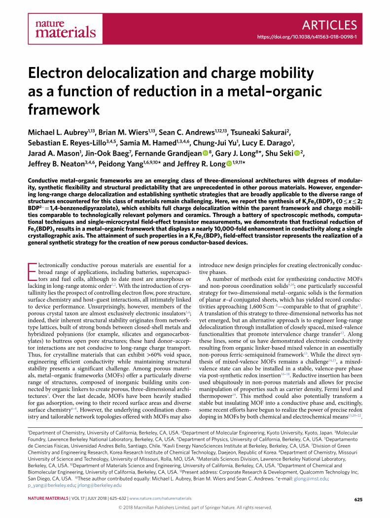
Electronic structure of the model system KxFe(pyrazolate)3Insight into the transport properties of KxFe2(BDP)3 was gained from density functional theory (DFT) calculations on a single one-dimensional chain with the formula Fe(pz)3, pz = pyrazo-late anion33, the electronic structure of which was found to well approximate that of the bulk framework near the Fermi level (Supplementary Tables 3 and 4 and Supplementary Fig. 9). Our calculations suggest that at low temperatures the iron ions cou-ple ferromagnetically along the chain (Supplementary Figs. 10 and 11); however, to agree with the room temperature measure-ments on the paramagnetic phase, all calculations of Fe(pz)3 were performed with an antiferromagnetic spin configuration (see Supplementary Information for an extended explanation). The band structure and projected density of states for the charge-neutral antiferromagnetic Fe(pz)3 revealed that orbitals centred on both the iron and pyrazolates contribute to the valence band maximum, as shown in Fig. 4a and Supplementary Figs. 12–14. Notably, the many weakly dispersive bands indicate a particularly localized electronic structure, with the exception of a single set of bands with a maximum at the Γ − point characteristic of a d–π symmetric state running down to the Η -point with a bandwidth of ~1 eV. Relaxation of the atomic coordinates after the addition of one extra electron to a six-iron supercell [Fe(pz)3]6—mimicking framework reduction on potassium insertion—leads to the forma-tion of an electron polaron, a localized quasiparticle composed of the electron and its self-induced lattice distortion34–36 (Fig. 4b). Closer examination of this polaronic charge density distribution indicates significant hybridization between iron-dπ and pyrazo-late π-states. This hybridization matches nicely with that expected for an octahedral low-spin d6 metal complex bonded to a π-acidic azolate, and small polaron formation is consistent with a mobil-ity-limited charge hopping mechanism for conduction along the iron–pyrazolate chains. The relatively small computed polaron acti-vation energy further supports the possibility of electron itineracy near room temperature, as corroborated experimentally by near- infrared/mid-infrared and Mössbauer absorption spectroscopy.
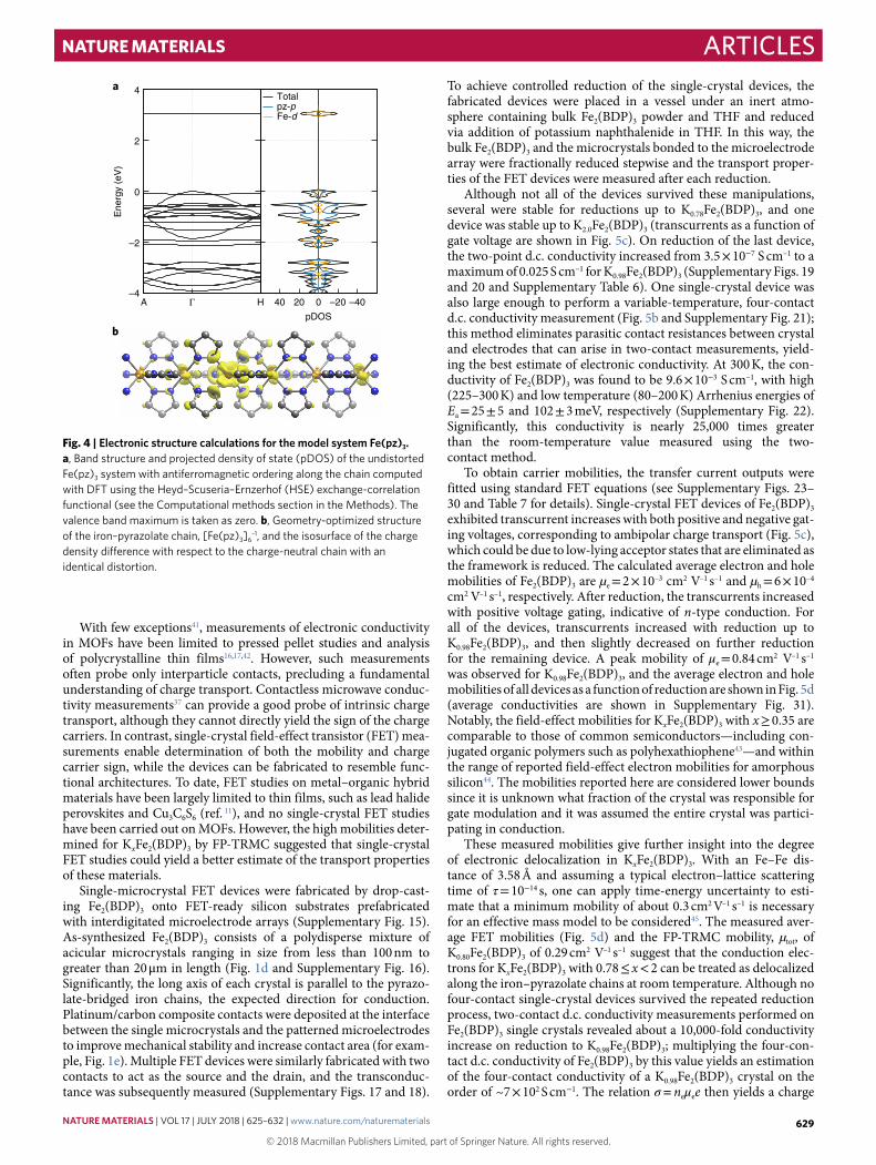
Conductivity and charge mobility in bulk KxFe2(BDP)3Flash photolysis time-resolved microwave conductivity (FP-TRMC)37,38 measurements were used to gain insight into the intrinsic charge transport characteristics of KxFe2(BDP)3. The phase Fe2(BDP)3 itself is intrinsically conductive, with a charge mobility (µtot) of 0.02 cm2 V–1 s–1, and on reduction the charge mobility increases to a maximum value of 0.29 cm2 V–1 s–1 for K0.8Fe2(BDP)3. The conductivity transients and calculated charge mobilities for KxFe2(BDP)3 (x = 0, 0.2, 0.4, and 0.8) are shown in Fig. 5a, and all measured mobility values are comparable to those of common organic conductors such as rubrene (0.05 cm2 V–1 s–1)39 and poly(p-phenylene vinylene) (0.1 cm2 V–1 s–1)40.
1.5 2.0 2.5 3.0
–15
–10
–5
0
5
I (m
A g
–1)
Potential versus K/K+ (V)
Reduction
Oxidation
x = 0
x = 2.02
99
100
−6 −5 −4 −3 −2 −1 0 2 6
Velocity (mm s–1)
93949596979899
100
98
99
100
Per
cent
tran
smis
sion
Per
cent
tran
smis
sion
Per
cent
tran
smis
sion
Per
cent
tran
smis
sion
97
98
99
100
x = 1.1
x = 0.0
x = 0.4
x = 2.0
a
b
5431
Fig. 3 | Mössbauer spectra and cyclic voltammogram of KxFe2(BDP)3. a, The 290 K Mössbauer spectra for KxFe2(BDP)3 for the x values shown. The red and green doublet fits correspond to low-spin iron(III) and high-spin iron(II) spectral components, respectively. b, Slow-scan cyclic voltammograms of Fe2(BDP)3 at 10 µ V s−1 with a 0.1 M K(TFSI), TFSI = bis(trifluoromethanesulfonyl)imide, in propylene carbonate electrolyte.
© 2018 Macmillan Publishers Limited, part of Springer Nature. All rights reserved.
NATuRE MATERiALS | VOL 17 | JULY 2018 | 625–632 | www.nature.com/naturematerials628
ArticlesNature Materials
With few exceptions41, measurements of electronic conductivity in MOFs have been limited to pressed pellet studies and analysis of polycrystalline thin films16,17,42. However, such measurements often probe only interparticle contacts, precluding a fundamental understanding of charge transport. Contactless microwave conduc-tivity measurements37 can provide a good probe of intrinsic charge transport, although they cannot directly yield the sign of the charge carriers. In contrast, single-crystal field-effect transistor (FET) mea-surements enable determination of both the mobility and charge carrier sign, while the devices can be fabricated to resemble func-tional architectures. To date, FET studies on metal–organic hybrid materials have been largely limited to thin films, such as lead halide perovskites and Cu3C6S6 (ref. 11), and no single-crystal FET studies have been carried out on MOFs. However, the high mobilities deter-mined for KxFe2(BDP)3 by FP-TRMC suggested that single-crystal FET studies could yield a better estimate of the transport properties of these materials.
Single-microcrystal FET devices were fabricated by drop-cast-ing Fe2(BDP)3 onto FET-ready silicon substrates prefabricated with interdigitated microelectrode arrays (Supplementary Fig. 15). As-synthesized Fe2(BDP)3 consists of a polydisperse mixture of acicular microcrystals ranging in size from less than 100 nm to greater than 20 μ m in length (Fig. 1d and Supplementary Fig. 16). Significantly, the long axis of each crystal is parallel to the pyrazo-late-bridged iron chains, the expected direction for conduction. Platinum/carbon composite contacts were deposited at the interface between the single microcrystals and the patterned microelectrodes to improve mechanical stability and increase contact area (for exam-ple, Fig. 1e). Multiple FET devices were similarly fabricated with two contacts to act as the source and the drain, and the transconduc-tance was subsequently measured (Supplementary Figs. 17 and 18).
To achieve controlled reduction of the single-crystal devices, the fabricated devices were placed in a vessel under an inert atmo-sphere containing bulk Fe2(BDP)3 powder and THF and reduced via addition of potassium naphthalenide in THF. In this way, the bulk Fe2(BDP)3 and the microcrystals bonded to the microelectrode array were fractionally reduced stepwise and the transport proper-ties of the FET devices were measured after each reduction.
Although not all of the devices survived these manipulations, several were stable for reductions up to K0.78Fe2(BDP)3, and one device was stable up to K2.0Fe2(BDP)3 (transcurrents as a function of gate voltage are shown in Fig. 5c). On reduction of the last device, the two-point d.c. conductivity increased from 3.5 × 10⁻⁷ S cm–1 to a maximum of 0.025 S cm–1 for K0.98Fe2(BDP)3 (Supplementary Figs. 19 and 20 and Supplementary Table 6). One single-crystal device was also large enough to perform a variable-temperature, four-contact d.c. conductivity measurement (Fig. 5b and Supplementary Fig. 21); this method eliminates parasitic contact resistances between crystal and electrodes that can arise in two-contact measurements, yield-ing the best estimate of electronic conductivity. At 300 K, the con-ductivity of Fe2(BDP)3 was found to be 9.6 × 10⁻³ S cm–1, with high (225–300 K) and low temperature (80–200 K) Arrhenius energies of Ea = 25 ± 5 and 102 ± 3 meV, respectively (Supplementary Fig. 22). Significantly, this conductivity is nearly 25,000 times greater than the room-temperature value measured using the two- contact method.
To obtain carrier mobilities, the transfer current outputs were fitted using standard FET equations (see Supplementary Figs. 23–30 and Table 7 for details). Single-crystal FET devices of Fe2(BDP)3 exhibited transcurrent increases with both positive and negative gat-ing voltages, corresponding to ambipolar charge transport (Fig. 5c), which could be due to low-lying acceptor states that are eliminated as the framework is reduced. The calculated average electron and hole mobilities of Fe2(BDP)3 are µe = 2 × 10⁻³ cm2 V–1 s–1 and µh = 6 × 10⁻⁴ cm2 V–1 s–1, respectively. After reduction, the transcurrents increased with positive voltage gating, indicative of n-type conduction. For all of the devices, transcurrents increased with reduction up to K0.98Fe2(BDP)3, and then slightly decreased on further reduction for the remaining device. A peak mobility of μe = 0.84 cm2 V–1 s–1 was observed for K0.98Fe2(BDP)3, and the average electron and hole mobilities of all devices as a function of reduction are shown in Fig. 5d (average conductivities are shown in Supplementary Fig. 31). Notably, the field-effect mobilities for KxFe2(BDP)3 with x ≥ 0.35 are comparable to those of common semiconductors—including con-jugated organic polymers such as polyhexathiophene43—and within the range of reported field-effect electron mobilities for amorphous silicon44. The mobilities reported here are considered lower bounds since it is unknown what fraction of the crystal was responsible for gate modulation and it was assumed the entire crystal was partici-pating in conduction.
These measured mobilities give further insight into the degree of electronic delocalization in KxFe2(BDP)3. With an Fe–Fe dis-tance of 3.58 Å and assuming a typical electron–lattice scattering time of τ = 10−14 s, one can apply time-energy uncertainty to esti-mate that a minimum mobility of about 0.3 cm2 V–1 s–1 is necessary for an effective mass model to be considered45. The measured aver-age FET mobilities (Fig. 5d) and the FP-TRMC mobility, µtot, of K0.80Fe2(BDP)3 of 0.29 cm2 V–1 s–1 suggest that the conduction elec-trons for KxFe2(BDP)3 with 0.78 ≤ x < 2 can be treated as delocalized along the iron–pyrazolate chains at room temperature. Although no four-contact single-crystal devices survived the repeated reduction process, two-contact d.c. conductivity measurements performed on Fe2(BDP)3 single crystals revealed about a 10,000-fold conductivity increase on reduction to K0.98Fe2(BDP)3; multiplying the four-con-tact d.c. conductivity of Fe2(BDP)3 by this value yields an estimation of the four-contact conductivity of a K0.98Fe2(BDP)3 crystal on the order of ~7 × 10² S cm−1. The relation σ = neμee then yields a charge
–4
–2
0
2
4a
b
A Γ H
Ene
rgy
(eV
)
40 20 0 –20 –40
Total
pDOS
pz-pFe-d
Fig. 4 | Electronic structure calculations for the model system Fe(pz)3. a, Band structure and projected density of state (pDOS) of the undistorted Fe(pz)3 system with antiferromagnetic ordering along the chain computed with DFT using the Heyd–Scuseria–Ernzerhof (HSE) exchange-correlation functional (see the Computational methods section in the Methods). The valence band maximum is taken as zero. b, Geometry-optimized structure of the iron–pyrazolate chain, [Fe(pz)3]6
–1, and the isosurface of the charge density difference with respect to the charge-neutral chain with an identical distortion.
© 2018 Macmillan Publishers Limited, part of Springer Nature. All rights reserved.
NATuRE MATERiALS | VOL 17 | JULY 2018 | 625–632 | www.nature.com/naturematerials 629

Articles Nature Materials
carrier density ne ~ 7 × 10²¹ e cm−3, a value comparable to the value of 9.2 × 10²⁰ e cm−3 that is estimated by dividing the potassium con-tent per unit cell by the unit-cell volume. This estimation indicates that at near half-reduction, the added electrons are delocalized over the framework as conduction electrons. In addition, two-contact, pressed pellet measurements of K0.98Fe2(BDP)3 (Supplementary Figs. 32 and 33) gave conductivities at least a million times lower than comparable two-contact single-crystal measurements, exem-plifying the extreme anisotropy of transport in these materials and suggesting that KxFe2(BDP)3 is a one-dimensional conductor.
OutlookThe path towards engendering long-range charge delocalization through the atomically thin pore walls of MOFs remains a chal-lenging endeavor. However, the control and precision that can be achieved through quantitative redox doping and single-crystal FET measurements prove these tools to be invaluable for maxi-mizing conductivity and understanding the underlying electronic structures of this relatively new class of materials. Here we found, by considering the structural motif [Fe(pz)3]∞ as an ideal precur-sor to a conductive mixed-valence material, that sub-stoichiomet-ric reduction of Fe2(BDP)3 yielded both high charge mobilities for a porous conductor and the onset of carrier itineracy at ambient temperatures. Further, the modular [Fe(pz)3]∞ building unit may be more easily incorporated into new frameworks of differing topology and surface chemistry than the subunits of some of the most con-ductive MOF structure types reported46. Indeed, only MOFs such as KxFe2(BDP)3 with open, three-dimensional networks can fully
realize the synthetic control and diversity of properties that conduc-tive coordination solids have to offer. More broadly, the installation of a repeat mixed-valence substructure is an intuitive and viable mode for building tunable, porous conductor-based devices from well-established models of charge delocalization in coordination chemistry12. By extending the frontier states across multiple repeat units along at least one framework dimension through metal–ligand hybridization, band dispersion can be increased significantly. In doing so, porous crystals may approach the interface between localized—molecule-like—interactions and the broad band disper-sion found in classical conductors, all while retaining the poros-ity, surface chemistry and host–guest chemistry for which MOFs are unique.
MethodsMethods, including statements of data availability and any asso-ciated accession codes and references, are available at https://doi.org/10.1038/s41563-018-0098-1.
Received: 14 August 2017; Accepted: 30 April 2018; Published online: 4 June 2018
References 1. Tian, Z.-R. et al. Manganese oxide mesoporous structures: mixed-valent
semiconducting catalysts. Science 276, 926–930 (1997). 2. Pandolfo, A. G. & Hollenkamp, A. F. Carbon properties and their role in
supercapacitors. J. Power Sources 157, 11–27 (2006). 3. Davis, M. E. Ordered porous materials for emerging applications. Nature 417,
813–821 (2002).
0 5 10
0
2
4
6
8
10
a b
c d
Time (μs)
x = 0.8 – 0.29 cm2 V–1 s–1
�Σμ
(×10
–5 c
m2 V
–1 s
–1) x = 0.4 – 0.09 cm2 V–1 s–1
x = 0.2 – 0.04 cm2 V–1 s–1
x = 0.0 – 0.02 cm2 V–1 s–1
50 100 150 200 250 300
10–6
10–5
10–4
10–3
10–2
T (K)
x = 0
σ (S
cm
–1)
–30 –20 –10 20 30
10–10
10–9
10–8
10–7
10–6
10–5
10–4
10–3
I SD (
A)
VG (V)
x = 0 x = 0.98x = 0.19 x = 1.35x = 0.35 x = 1.64x = 0.78 x = 1.96
0 10 0.0 0.5 1.0 1.5 2.010–4
10–3
10–2
10–1
100
Electron mobilityHole mobility
x in KxFe2 (BDP)3
μ (c
m2 V
–1 s
–1)
Fig. 5 | Characterization of charge transport in KxFe2(BDP)3. a, Conductivity transients observed by flash photolysis time-resolved microwave spectroscopy on excitation at 355 nm with 6.5 × 10¹⁵ photons cm−2 per pulse for KxFe2(BDP)3 (x = 0, 0.2, 0.4 and 0.8). b, Four-point d.c variable-temperature single-crystal conductivity measurements of Fe2(BDP)3. c, Voltage-gated transcurrents of KxFe2(BDP)3 (x = 0, 0.19, 0.35, 0.78, 0.98, 1.35, 1.64 and 1.96) for a single-crystal FET device. VSD = 1 V. d, Average FET hole and electron mobilities of single-crystal KxFe2(BDP)3 devices as a function of x. The mobility error bars are given as the standard deviation of the set of unique devices measured at each stoichiometry; the x error bars are given as the standard deviation in stoichiometry across multiple locations on the devices measured.
© 2018 Macmillan Publishers Limited, part of Springer Nature. All rights reserved.
NATuRE MATERiALS | VOL 17 | JULY 2018 | 625–632 | www.nature.com/naturematerials630

ArticlesNature Materials
4. Usman, M., Mendirata, S. & Lu, K.-L. Metal–organic frameworks: new interlayer dielectric materials. ChemElectroChem 2, 786–788 (2015).
5. Long, J. R. & Yaghi, O. M. The pervasive chemistry of metal–organic frameworks. Chem. Soc. Rev. 38, 1213–1214 (2009).
6. Sculley, J., Yang, D. & Zhou, H.-C. The current status of hydrogen storage in metal–organic frameworks, updated. Energy Environ. Sci. 4, 2721–2735 (2011).
7. Eddaoudi, M. et al. Systematic design of pore size and functionality in isoreticular MOFs and their application in methane storage. Science 295, 469–472 (2002).
8. Matsuda, R. et al. Highly controlled acetylene accommodation in a metal–organic microporous material. Nature 436, 238–241 (2005).
9. Sun, L., Campbell, M. G. & Dincă, M. Electrically conductive porous metal–organic frameworks. Angew. Chem. Int. Ed. 55, 3566–3579 (2016).
10. Givaja, G., Amo-Ochoa, P., Gómez-García, C. J. & Zamora, F. Electrical conductive coordination polymers. Chem. Soc. Rev. 41, 115–147 (2012).
11. Huang, X. et al. A two-dimensional π–d conjugated coordination polymer with extremely high electrical conductivity and ambipolar transport behaviour. Nat. Commun. 6, 7480 (2015).
12. D’Alessandro, D. M., Kanga, J. R. R. & Caddy, J. S. Towards conducting metal–organic frameworks. Aust. J. Chem. 64, 718–722 (2011).
13. Darago, L. E., Aubrey, M. L., Yu, C. J., Gonzalez, M. I. & Long, J. R. Electronic conductivity, ferrimagnetic ordering, and reductive insertion mediated by organic mixed-valence in a ferric semiquinoid metal–organic framework. J. Am. Chem. Soc. 137, 15703–15711 (2015).
14. D’Alessandro, D. M. Exploiting redox activity in metal–organic frameworks: concepts, trends and perspectives. Chem. Commun. 52, 8957–8971 (2016).
15. Horike, S. et al. Fe2+-based layered porous coordination polymers and soft encapsulation of guests via redox activity. J. Mater. Chem. A 1, 3675–3679 (2013).
16. Kobayashi, Y., Jacobs, B., Allendorf, M. D. & Long, J. R. Conductivity, doping, and redox chemistry of a microporous dithiolene-based metal–organic framework. Chem. Mater. 22, 4120–4122 (2010).
17. Gándara, F. et al. Porous, conductive metal-triazolates and their structural elucidation by the charge-flipping method. Chem. Eur. J. 18, 10595–10601 (2012).
18. Meilikhov, M. et al. Reduction of a metal–organic framework by an organometallic complex: magnetic properties and structure of the inclusion compound [(η 5-C5H5)2Co]0.5@MIL-47(V). Angew. Chem. Int. Ed. 49, 6212–6215 (2010).
19. Jacobson, A. J. & Nazar, L. F. in Encyclopedia of Inorganic and Bioinorganic Chemistry https://doi.org/10.1002/9781119951438.eibc0093 (Wiley, Medford, MA, 2006).
20. Férey, G. et al. Mixed-valence Li/Fe-based metal–organic frameworks with both reversible redox and sorption properties. Angew. Chem. Int. Ed. 46, 3259–3263 (2007).
21. Aubrey, M. L. & Long, J. R. A dual-ion battery cathode via oxidative insertion of anions in metal–organic framework. J. Am. Chem. Soc. 137, 13594–13602 (2015).
22. Kung, C.-W. et al. Metal–organic framework thin films composed of free-standing acicular nanorods exhibiting reversible electrochromism. Chem. Mater. 25, 5012–5017 (2013).
23. Creutz, C. Mixed valence complexes of d5–d6 metal centers. Prog. Inorg. Chem. 30, 1–73 (1983).
24. Herm, Z. R. et al. Separation of hexane isomers in a metal–organic framework with triangular channels. Science 340, 960–964 (2013).
25. Feller, R. K. & Cheetham, A. K. Fe(III), Mn(II), Co(II), and Ni(II) 3,4,5-trihydroxybenzoate (gallate) dihydrates; a new family of hybrid framework materials. Solid State Sci. 8, 1121–1125 (2006).
26. Sun, L., Hendon, C. H., Minier, M. A., Walsh, A. & Dincă, M. Million-fold electrical conductivity enhancement in Fe2(DEBDC) versus Mn2(DEBDC) (E = S, O). J. Am. Chem. Soc. 137, 6164–6167 (2015).
27. Mason, J. A. et al. Methane storage in flexible metal–organic frameworks with intrinsic thermal management. Nature 527, 357–361 (2015).
28. Torrance, J. B., Scott, B. A., Welber, B., Kauffman, F. B. & Seiden, P. E. Optical properties of the radical cation tetrathiafulvalenium (TTF+) in its mixed valence and monovalence halide salts. Phys. Rev. B 19, 730–741 (1979).
29. Parthey, M. & Kaupp, M. Quantum-chemical insight into mixed-valence systems within and beyond the Robin-Day scheme. Chem. Soc. Rev. 43, 5067–5088 (2014).
30. Collman, J. P. et al. Synthetic, electrochemical, optical, and conductivity studies of coordination polymers of iron, ruthenium, and osmium octaethylporphyrin. J. Am. Chem. Soc. 109, 4606–4614 (1987).
31. Tanner, D. B., Jacobsen, C. S., Garito, A. F. & Heeger, A. J. Infrared studies of the energy gap in tetrathiofulvalene-tetracyanoquinodimethane (TTF-TCNQ). Phys. Rev. B 13, 3381–3404 (1976).
32. Fincher, C. R. Jr., Ozaki, M., Heeger, A. J. & MacDiarmid, A. G. Donor and acceptor states in lightly doped polyacetylene, (CH)x. Phys. Rev. B 19, 4140–4148 (1979).
33. Masciocchi, N. et al. One-dimensional polymers containing strictly collinear metal ions: synthesis and XRPD characterization of homoleptic binary metal pyrazolates. Inorg. Chem. 41, 6080–6089 (2002).
34. Maxisch, T., Zhou, F. & Ceder, G. Ab initio study of the migration of small polarons in olivine LixFePO4 and their association with lithium ions and vacancies. Phys. Rev. B 73, 104301 (2006).
35. Alexandrov, V., Neumann, A., Scherer, M. M. & Rosso, K. M. Electron exchange and conduction in nontronite from first-principles. J. Phys. Chem. C 117, 2032–2040 (2013).
36. Adelstein, N., Neaton, J. B., Asta, M. & De Jonghe, L. C. Density functional theory based calculation of small-polaron mobility in hematite. Phys. Rev. B 89, 245115-1 (2014).
37. Narayan, T. C., Miyaki, T., Seki, S. & Dincă, M. High charge mobility in a tetrathiafulvalene-based metal–organic framework. J. Am. Chem. Soc. 134, 12933–12935 (2012).
38. Saeki, A., Koizumi, Y., Aida, T. & Seki, S. Comprehensive approach to intrinsic charge carrier mobility in conjugated organic molecules, macromolecules, and supramolecular architectures. Acc. Chem. Res. 45, 1193–1202 (2012).
39. Saeki, A., Seki, S., Takenobu, T., Iwasa, Y. & Tagawa, S. Mobility and dynamics of charge carriers in rubrene single crystals studied by flash-photolysis microwave conductivity and optical spectroscopy. Adv. Mater. 20, 920–923 (2008).
40. Krebs, F. C. & Jørgensen, M. High carrier mobility in a series of new semiconducting PPV-type polymers. Macromolecules 36, 4379–4384 (2003).
41. Park, S. S. et al. Cation-dependent intrinsic electrical conductivity in isostructural tetrathiafulvalene-based microporous metal–organic frameworks. J. Am. Chem. Soc. 137, 1774–1777 (2015).
42. Talin, A. A. et al. Tunable electrical conductivity in metal–organic framework thin-film devices. Science 343, 66–69 (2014).
43. Sirringhaus, H. et al. Two-dimensional charge transport in self-organized, high-mobility conjugated polymers. Nature 401, 685–688 (1999).
44. Kanicki, J., Libsch, F. R., Griffith, J. & Polastre, R. Performance of thin hydrogenated amorphous silicon thin-film transistors. J. Appl. Phys. 69, 2339–2345 (1991).
45. Bright, A., Chaikin, P. M. & McGhie, A. R. Photoconductivity and small-polaron effects in tetracyanoquinodimethane. Phys. Rev. B 10, 3560–3568 (1974).
46. Sheberla, D. et al. High electrical conductivity in Ni3(2,3,6,7,10,11-hexaminotriphenylene)2, a semiconducting metal–organic graphene analogue. J. Am. Chem. Soc. 136, 8859–8862 (2014).
AcknowledgementsSynthesis and characterization of the bulk materials was supported by the National Science Foundation through grant DMR-1611525. Additional efforts to synthesize the materials in nanocrystalline form were funded by a grant from the Go KRICT Project for Future Technology of the Korea Research Institute of Chemical Technology (KRICT). We thank G. Halder for assisting with powder diffraction experiments, which were collected at Beamline 17-BM-B at the Advanced Photon Source, a DoE Office of Science User Facility operated by Argonne National Laboratory under contract no. DE-AC02-06CH11357. S.E.R.-L. and S.M.H. thank R. F. Berger and K. Lee for valuable discussions. Theory and computation were supported by the US Department of Energy, Office of Science, Office of Basic Energy Sciences (Theory FWP) Materials Sciences and Engineering Division (DE-AC02-05CH11231). Work at the Molecular Foundry was supported by the Office of Science, Office of Basic Energy Sciences, of the US Department of Energy under contract no. DE-AC02-05CH11231. Portions of the computation work were performed at the Molecular Graphics Facility at the Department of Chemistry of UC Berkeley. Support for FP-TRMC measurements conducted by S.S. and T.S. was funded by Japan Society for the Promotion of Science (JSPS) grant no. 15K21721. The FET part was supported by the US Department of Energy, Office of Science, Basic Energy Sciences, Materials Sciences and Engineering Division under contract no. DE-AC02-05CH11231 (PChem KC3103). We further thank Arkema for fellowship support of M.L.A., the NSF GRFP for fellowship support of L.E.D and J.A.M., and K. R. Meihaus for editing assistance.
Author contributionsM.L.A. developed the electrochemical experiments, helped to determine the electronic structure and transport mechanism, coordinated the collaboration and wrote the manuscript. B.M.W., S.C.A., P.Y. and J.R.L. conceived of the idea and designed the study, B.M.W. synthesized and collected spectroscopic measurements, determined surface areas and coordinated the collaboration. S.C.A. fabricated and measured the FET devices, T.S. and S.S. conducted the FP-TRMC measurements, S.E.R.-L., S.M.H. and J.B.N. completed the theoretical computations, C.-J.Y conducted the electrochemical measurements, L.E.D. conducted the magnetic susceptibility measurements and helped determined the magnetic structure of the material, J.A.M. conducted the X-ray
© 2018 Macmillan Publishers Limited, part of Springer Nature. All rights reserved.
NATuRE MATERiALS | VOL 17 | JULY 2018 | 625–632 | www.nature.com/naturematerials 631

Articles Nature Materials
diffraction measurements, J.-O.B. helped conceive of the idea, and elucidate the transport mechanism, F.G. and G.J.L modelled the Mössbauer spectra, and determined the magnetic and electronic structure of the material. G.J.L, P.Y. and J.R.L. supervised and guided the project. All authors helped write the manuscript.
Competing interestsThe authors declare no competing interests.
Additional informationSupplementary information is available for this paper at https://doi.org/10.1038/s41563-018-0098-1.
Reprints and permissions information is available at www.nature.com/reprints.
Correspondence and requests for materials should be addressed to G.J.L. or P.Y. or J.R.L.
Publisher’s note: Springer Nature remains neutral with regard to jurisdictional claims in published maps and institutional affiliations.
© 2018 Macmillan Publishers Limited, part of Springer Nature. All rights reserved.
NATuRE MATERiALS | VOL 17 | JULY 2018 | 625–632 | www.nature.com/naturematerials632

ArticlesNature Materials
MethodsGeneral considerations. Bulk reduction of the MOF, structural characterization, gas adsorption uptake, magnetic characterization, electrochemical measurements, electrical conductivity, and FET fabrication and analysis have been performed as described in our previous report47. The detailed method is reproduced here for completeness. Unless otherwise specified, all manipulations were performed with rigorous exclusion of air and water by use of inert atmosphere (Ar/N2) gloveboxes and Schlenk techniques. Reagents were purchased from commercial vendors and used without further purification. N,N-dimethylformamide (DMF), methanol and THF were deoxygenated by purging with argon for 1 h and dried using a commercial solvent purification system designed by JC Meyer Solvent Systems. Inductively coupled plasma optical emission spectroscopy (ICP-OES) was performed on a Perkin Elmer Optima 7000 DV ICP-OES in the Department of Chemistry at the University of California, Berkeley on samples of KxFe2(BDP)3 digested by treatment with 40 wt% H2O2 in H2O followed by addition of 37 wt% HCl in H2O. Energy-dispersive spectroscopy (EDS) spectra were taken using a JEOL JSM-6340F field-emission scanning electron microscope equipped with an EDAX Falcon detector. Fe2(BDP)3 was prepared as previously reported24.
Bulk reduction of Fe2(BDP)3. A 0.1 M solution of potassium naphthalenide, with a 10% molar excess of naphthalene in THF was prepared immediately before use. Weighed aliquots of activated Fe2(BDP)3 were suspended in 10 ml of THF with magnetic stirring. Measured amounts of potassium naphthalenide solution were then added to the Fe2(BDP)3 suspensions to target desired stoichiometries. The potassium naphthalenide was not added all at once, but rather in three to four portions over the course of 1–2 h as the suspensions were stirred. The suspensions with the added potassium naphthalenide solutions were stirred overnight. The solid was then collected and repeatedly washed with THF until the THF washes showed no more presence of naphthalene. PXRD measurements showed the preservation of crystallinity, and potassium to iron ratios were confirmed by ICP-OES and EDS.
PXRD. Synchrotron PXRD measurements were carried out on Beamline 17-BM-B (λ = 0.72959 Å) at the Advanced Photon Source at Argonne National Laboratory. Samples of solvated KxFe2(BDP)3 at different levels of reduction were loaded into 1.0 mm borosilicate capillaries inside a nitrogen glovebox and flame-sealed before all PXRD measurements. A standard peak search, followed by indexing via the single-value decomposition approach48,49, as implemented in TOPAS-Academic50, allowed the determination of approximate unit-cell dimensions. Precise unit-cell dimensions were determined by performing a structureless Le Bail refinement in TOPAS-Academic. Note that a single weak anomalous peak is observed at ~8.5° in several of the PXRD patterns (x = 0.9, 1.3, 1.4, 2.0). This peak can probably be attributed to poorly ordered solvated K+ cations in the framework pores or a slight distortion (and corresponding reduction in symmetry) of the partially solvated framework structure, and as such, it is not expected to affect any spectroscopic, electrochemical or electron-transport results.
Low-pressure gas adsorption measurements. For all gas adsorption measurements, 200–225 mg of KxFe2(BDP)3 was transferred to a pre-weighed glass sample tube under an atmosphere of nitrogen and the tube was capped with a Transeal. Samples were then transferred to a Micromeritics ASAP 2020 gas adsorption analyser and heated at a rate of 1 °C min−1 from room temperature to a final temperature of 180 °C. Samples were considered activated when the outgas rate at 150 °C was less than 2 μ bar min−1, which occurred nearly 48 h after the start of evacuation. Evacuated tubes containing degassed samples were then transferred to a balance and weighed to determine the mass of sample. The tube was transferred to the analysis port of the instrument where the outgas rate was again determined to be less than 2 μ bar min−1 at 180 °C. 99.999% purity gas was used for nitrogen adsorption.
Ultraviolet−visible−near-infrared diffuse reflectance spectra. Ultraviolet− visible− near-infrared diffuse reflectance spectra were collected using a CARY 5000 spectrophotometer interfaced with Varian Win UV software. The samples were held in a Praying Mantis air-free diffuse reflectance cell. On exposure to atmosphere, the potassium-reduced KxFe2(BDP)3 was gradually oxidized and the originally observed absorption edge for Fe2(BDP)3 returned (Supplementary Fig. 34). Polyvinylidene fluoride powder was used as a non-absorbing matrix. The Kubelka–Munk conversion, F(R) versus wavenumber, of the raw diffuse reflectance spectrum (R versus wavenumber) was obtained by applying the formula F(R) = (1 − R)2/2 R. This transform creates a linear relationship for the spectral intensity relative to sample concentration and assumes that the sample is infinitely diluted in the non-absorbing matrix, that the sample layer is ‘infinitely thick’ and that the sample has a constant scattering coefficient.
Fourier-transform infrared spectra. Infrared spectra were recorded on a Perkin Elmer Spectrum 400 FTIR spectrophotometer equipped with an attenuated total reflectance accessory. A dinitrogen-purged glove bag was attached to the attenuated total reflectance accessory to allow air- and water-free measurements of spectra.
Magnetic measurements. The sample was prepared by adding crystalline powder of the parent framework Fe2(BDP)3 (12.1 mg) to a quartz tube (of 5 mm inner diameter) containing a raised quartz platform. A compressed plug of glass wool was added to cover the sample to prevent crystallite torquing. The tube was fitted with a Teflon sealable adapter, evacuated on a Schlenk line, and flame-sealed under static vacuum. Magnetic susceptibility measurements were performed using a Quantum Design MPMS2 SQUID magnetometer. d.c. magnetic susceptibility measurements were collected in the temperature range 2–300 K under applied magnetic fields of 0.1 T, 1 T and 7 T. Magnetic hysteresis measurements were performed at a field sweep rate of 0.27 mT s−1. Diamagnetic corrections were applied to the data using Pascal's constants to give χD = − 0.00036164 emu mol−1 (Fe2(BDP)3).
Mössbauer spectral measurements and analysis. The Mössbauer spectra of KxFe2(BDP)3 were obtained at 290 K with a SEE Mössbauer spectrometer equipped with a Co-57 in Rh source over the velocity range of ± 12 mm s−1. This large velocity range was used to detect the presence of any magnetically ordered spectral components—none was observed at 290 K. The pertinent spectral components are all found between ± 6 mm s−1. The isomer shifts are given relative to α -iron at 290 K.
The spectral absorbers were prepared in an argon-atmosphere glovebox by intimately grinding a mixture of the sample and boron nitride powder and packing the mixture into a 2.54-cm-diameter polypropylene washer that was sealed with three layers of packing tape before transfer to the spectrometer where the absorber was always maintained in a helium atmosphere to prevent oxidation or decomposition.
The resulting Mössbauer spectra were fitted with the minimum number of quadrupole doublets needed to fit the observed spectral profile within a model compatible with the crystallographic structure and the electronic configuration of the iron ions; constraints have been applied to minimize the number of variable parameters (that is, a single linewidth was used for all iron(II) or iron(III) doublets and, for 0.2 ≤ x ≤ 0.8, the iron(III) doublets all had the same isomer shift). All of the doublets are symmetric, except for 0.2 ≤ x ≤ 0.8, for which an area ratio of the left to the right line of 0.87, resulting from texture, was introduced into the fits. Such texture is consistent with the morphology of the sample crystals as is indicated in Fig. 1d.
The observed hyperfine parameters are all consistent with the presence of S = ½ low-spin iron(III) and S = 2 high-spin iron(II) ions but the fits do not exclude the unexpected presence of S = 0 low-spin iron(II) ions.
The compositional dependence of the weighted average low-spin iron(III) isomer shift (see Supplementary Fig. 4) exhibits a small increase with increasing x from 0.065 to 0.165 mm s−1, an increase that indicates a decrease in the s-electron density at the iron-57 nucleus. The average high-spin iron(II) isomer shifts for 0.9 ≤ x ≤ 2.0 are, within their uncertainties, essentially independent of x. The compositional dependence of the weighted average low-spin iron(III) quadrupole splitting (see Supplementary Fig. 4) shows a clear decrease at x = 0.9, a potassium content for which a reconstitution reaction is observed in the cyclic voltammetry measurements (see Fig. 3b). Then the spectra for 0.9 ≤ x ≤ 1.7 remain essentially unchanged with x in agreement with the plateau observed in the current integration for the slow-scan cyclic voltammogram shown in Supplementary Fig. 8.
Electrochemical measurements. In an argon glovebox, cyclic voltammetry was conducted in a custom-built perfluoroalkoxy ethane T-cell with titanium current collectors. Potassium metal, polished to a mirror finish, was used as the reference and counter electrodes. The working electrode was prepared by drop casting a slurry of 60 wt% Fe2(BDP)3, 30 wt% Super P (Fischer) and 10 wt% polyvinylidene fluoride (Aldrich) suspended in THF onto carbon cloth (Fuel Cell Earth). The electrode was desolvated at 180 °C for approximately 2 h, and then loaded into the T-cell. Electrodes were separated by a quartz fibre separator saturated with a 0.1 M solution of K(TFSI) (STREM) in anhydrous propylene carbonate (Aldrich). Cells were set to relax at open-circuit potential to a limiting condition of 0.1 mV h−1 before measurement. Slow-scan cyclic voltammetry was performed using a Bio-Logic VMP-3 multipotentiostat. Cyclic voltammograms were collected with an IR drop correction determined by single-point potentiostatic a.c. impedance measurement at 10 mV a.c. and 0 V versus open circuit. Near-equilibrium conditions were observed for sweep rates of 0.1 mV s−1 and slower for the material KxFe2(BDP)3 for the range 0 ≤ x ≤ 1.95.
Computational methods. To investigate the transport properties of the KxFe2(BDP)3 system, spin-polarized DFT calculations are performed on Fe2(BDP)3 and the smaller model system Fe(pz)3 (ref. 33). Fe(pz)3 corresponds to an experimentally realizable one-dimensional chain structure with Fe–Fe distances and Fe coordination environments similar to Fe2(BDP)3. The structures of the extended Fe2(BDP)3 and chain Fe(pz)3 systems are shown in Supplementary Fig. 9.
DFT calculations for the periodic Fe2(BDP)3 and Fe(pz)3 systems are performed with VASP51. Our DFT calculations use the generalized gradient approximation (GGA)52 plus Hubbard U approach (GGA + U)53 with the rotationally invariant method of ref. 54. Hybrid functionals partially mitigate the inherent self-interaction error of standard semilocal functionals such as GGA + U and can
© 2018 Macmillan Publishers Limited, part of Springer Nature. All rights reserved.
NATuRE MATERiALS | www.nature.com/naturematerials

Articles Nature Materials
significantly improve the description of charge localization in transition metal oxides. Therefore, excess charge simulations are performed with the HSE hybrid functional55, where 25% of the GGA is replaced with exact Hartree–Fock exchange, and the long-range interaction is screened with a range separation parameter of 0.2 Å–1. An extended discussion of the DFT results can be found in the Supplementary Information. Supplementary Figs. 10 and 11 report GGA + U total energy calculations for different magnetic configurations of Fe2(BDP)3 and Fe(pz)3, respectively. Supplementary Fig. 12 shows projected density of states for Fe2(BDP)3 and Fe(pz)3 using GGA + U and HSE, respectively. Supplementary Figs. 13 and 14 gives band structure calculations for pristine and doped Fe(pz)3, respectively, obtained by using HSE.
FP-TRMC measurements. FP-TRMC measurements were conducted at 25 °C under a N2 atmosphere, using Fe2(BDP)3/poly(methylmethacrylate) (PMMA) films (50/50 in wt%). The films were cast onto quartz substrates. The microwave power and frequency were set at 3 mW and ~9.1 GHz, respectively. Charge carriers were generated in the films by direct excitation of MOFs using third-harmonic generation (λ = 355 nm) light pulses from a Nd:YAG laser (Spectra Physics, INDI-HG). The excitation density was tuned at 6.5 × 10¹⁵ photons cm–2 pulse–1. The TRMC signal from a diode was recorded on a digital oscilloscope (Tektronix, TDS 3032B). To determine the quantum efficiency of charge carrier generation, the Fe2(BDP)3/PMMA films were deposited on gold interdigitated electrodes (electrode separation = 5 μ m) and the photocurrent was measured on irradiation with a 355 nm pulse. Comparison of the integrated photocurrents with the polymer standard (poly)9,9′ -dioctylfluorene, ϕ ~ 2.3 × 10⁻⁴) allowed determination of the quantum efficiency of charge carrier generation for the KxFe2(BDP)3 samples. The local-scale charge carrier mobility μtot was estimated by the quotient of (ϕΣ μ)max by ϕ.
Sequential reduction and measurement of single-crystal Fe2(BDP)3 FETs. After initial measurements were performed on unreduced single-crystal devices, the FETs on microelectrode arrays were brought into a dinitrogen glovebox and placed into a 100-ml borosilicate glass jar with 50 ml of THF and 300 mg of Fe2(BDP)3. The chip was surrounded with pierced aluminium foil, taking care not to contact the foil with the chips. The foil housing the microelectrode arrays served to prevent mechanical abrasion of the chips while allowing access to the reductant solution. About 20 ml of a freshly prepared 0.07 M potassium naphthalenide solution was added to the jar. The jar was capped and agitated by hand for 1 h and then allowed to sit overnight. The chips were then removed and rinsed five times with THF. An aliquot of the bulk Fe2(BDP)3 sample was then removed and analysed by EDS. EDS data were collected from the K K and the Fe K peaks of a 40 μ m × 40 μ m area for each sample at 20 kV and analysed using the software's true standardless-quantification mode. The ratios determined from the bulk aliquots were used to estimate the degree of reduction of single-crystal devices. To protect the devices from oxidation while transferring to the probe station, two drops of a polystyrene in toluene solution were added to the chips and allowed to dry in the dinitrogen-filled glovebox. This coating procedure was repeated twice and the sample was removed from the glovebox and transferred to the probe station. In the probe station, the probes pierced through the polystyrene coating through to the contact pads of the microelectrode array. After measurement, the chips were brought back into the dinitrogen glovebox and soaked in toluene for 20 min to dissolve the protective polystyrene coating. The chips were then rinsed gently two times with
toluene and two times with THF and then set to dry. They were again placed in a pierced aluminium foil protective covering and into the jar with excess Fe2(BDP)3 sample, and the procedure for stepwise reduction, protection and measurement of the devices was repeated.
Single-crystal FET and four-point device fabrication and measurements. Fe2(BDP)3 microcrystals were suspended in a 0.1 wt% dispersion in acetonitrile. Microcrystals were micro-manipulated between prefabricated electrodes on FET substrates (200 nm silicon dioxide). Loaded devices were placed into a FEI Strata 235 dual-beam focused ion beam and examined via the SEM in the system. To increase the electrical contact area and physical stability of the crystal on the device, electron-beam-induced deposition was used to place Pt/C pads at the interface of the crystal and the electrode on each side. Note that while this process was conducted within a FIB, only the SEM capabilities were used to avoid any potential ion beam damage. We note that no visible damage or changes were observed after 5 min of continuous 5.0 kV electron beam irradiation (Supplementary Fig. 18). The exposure times were limited to a maximum of 60 s at a time to limit potential migration of the deposited Pt away from the intended area. Once several bonds were created, many devices were robust enough for solution-based reduction and subsequent electrical measurements were performed on a 2636A Dual Channel Keithley SourceMeter in a home-built probe station. Variable-temperature conductivity data were fitted to an Arrhenius temperature dependence. An extended discussion describing the charge mobility calculation is included in the Supplementary Information.
Data availability. The experimental and computational data that support the findings of this study are available from the corresponding author upon request.
References 47. Wiers, B. M. Charge Transport in Metal-Organic Frameworks. PhD thesis,
Univ. California Berkeley (2015). 48. Coelho, A. Indexing of powder diffraction patterns by iterative use of singular
value decomposition. Appl. Cryst. 36, 86–95 (2003). 49. Cheary, R. W. & Coelho, A. A. Axial divergence in a conventional X-ray
powder diffractometer. I. Theoretical foundations. J. Appl. Crystallogr. 31, 851–861 (1998).
50. Coelho, A. TOPAS-Academic, v.4.1 (Coelho Software 2007). 51. Kresse, G. & Furthmüller, J. Efficient iterative schemes for ab initio
total-energy calculations using a plane-wave basis set. Phys. Rev. B 54, 11169–11186 (1996).
52. Perdew, J. P., Burke, K. & Ernzerhof, M. Generalized gradient approximation made simple. Phys. Rev. Lett. 77, 3865–3868 (1996).
53. Anisimov, V. I., Aryasetiawan, F. & Lichtenstein, A. I. First-principles calculations of the electronic structure and spectra of strongly correlated systems: the LDA + U method. J. Phys. Condens. Matter 9, 767–808 (1997).
54. Dudarev, S. L., Botton, G. A., Savrasov, S. Y., Humphreys, C. J. & Sutton, A. P. Electron-energy-loss spectra and the structural stability of nickel oxide: an LSDA + U study. Phys. Rev. B 57, 1505–1509 (1998).
55. Krukau, A. V., Vydrov, O. A., Izmaylov, A. F. & Scuseria, G. E. Influence of the exchange screening parameter on the performance of screened hybrid functionals. J. Chem. Phys. 125, 224106 (2006).
© 2018 Macmillan Publishers Limited, part of Springer Nature. All rights reserved.
NATuRE MATERiALS | www.nature.com/naturematerials