electro-thermal modelling of infrared microemitters using pspice
TRANSCRIPT

Ž .Sensors and Actuators A72 1999 110–114
Electro-thermal modelling of infrared microemitters using PSPICE
S. Ravi Kiran, G. Karunasiri )
Department of Electrical Engineering, Centre for Optoelectronics, National UniÕersity of Singapore, Singapore 119260, Singapore
Received 16 March 1998; revised 4 August 1998; accepted 7 August 1998
Abstract
The technology to simulate dynamic infrared scenes using an array of resistively heated microbridges has progressed rapidly in recentyears. This paper presents a technique to model the thermal and electrical properties of microemitters using PSPICE. The model providesan insight and understanding of many physical and dynamic properties of the pixel and is cost effective as both electrical and thermalsimulations can be performed in the same design environment. The various fabrication process parameters and operating conditions canbe fed to the model as user defined inputs and the application of this model can thus be extended to simulate variety of emitters.Theoretical and experimental data have been compared with simulation results and its excellent agreement verifies the validity of thePSPICE model. q 1999 Elsevier Science S.A. All rights reserved.
Keywords: Infrared; Microemitters; Scene generators; Thermal modelling; Bolometers; Micromachining
1. Introduction
The recent advances in micromachining technology haveenabled the fabrication of large arrays of resistor micro-bridges which offer much needed flexibility for dynamic
w xinfrared scene simulations 1–5 . These scene generatorsare essential for testing of real time performance of in-
w xfrared cameras 6,7 . The advantages of resistor arrays areevident as they are capable of producing high emittance
w xstructures with low electrical power consumption 5 . Eachpixel of the resistor array is essentially composed of asuspended resistor which is monolithically integrated with
w xCMOS control electronics 1 . The pixel control electronicsgoverns the current through the emitter resistor which inturn causes increase in emitter temperature due to Joule
Ž .heating or self-heating . A sharp increase of emitter tem-perature can be achieved using milliwatts of power bythermally isolating the emitter by silicon micromachiningw x1 . High optical emissivity can be achieved by incorporat-ing tuned cavity and deliberate selection of emitter mate-
w xrial and thin film membrane for suspension 1 . The pixelsin the resistor array can be selectively turned onroff witha digital control circuitry to project high resolution images.Thermal behaviour of emitters is often understood by
w xnumerically solving complex heat transfer equations 8 .
) Corresponding author. Tel.: q65-874-2162; Fax: q65-779-1103;E-mail: [email protected]
The analysis becomes even more complicated when theresponse of the emitter along with its control electronics isrequired. In this paper, we present a technique to simulateelectro-thermal behaviour of an infrared emitter usingPSPICE. The physical operation of the emitter is repre-sented by both linear and non-linear circuit elements andits thermal behaviour is simulated using equivalent electri-cal parameters. The simulation model is very versatile andwith the knowledge of process parameters and operatingconditions, various emitter characteristics can be under-stood and optimized. It was found that the simulatedresults are in close agreement with that of the experimental
w xfindings of Cole and Han 1 .
2. Electro-thermal modelling of emitter pixels
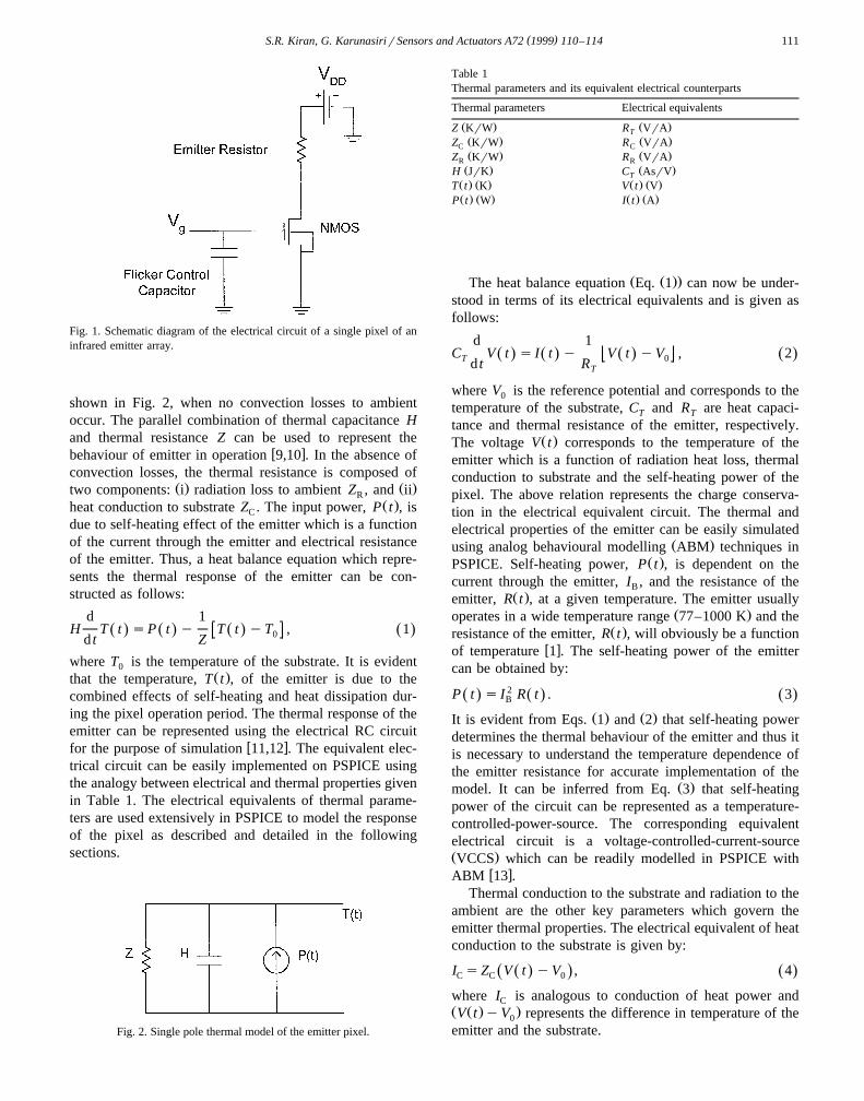
The pixel of an infrared scene generator array is typi-cally composed of an emitter connected in series to a drive
Ž .n-MOSFET NMOS as illustrated in Fig. 1. An analogsignal voltage containing temperature information is kepton the gate of the drive transistor with a pixel hold
w xcapacitor to reduce the flicker 4 . The emitter, which ismicromachined over CMOS control electronics, achievessharp temperature rise due to self-heating. This heat isdissipated via conduction to the substrate and radiation tothe ambient. The thermal response of the emitter in vac-uum can thus be approximated with a single pole model as
0924-4247r99r$ - see front matter q 1999 Elsevier Science S.A. All rights reserved.Ž .PII: S0924-4247 98 00215-5
( )S.R. Kiran, G. KarunasirirSensors and Actuators A72 1999 110–114 111
Fig. 1. Schematic diagram of the electrical circuit of a single pixel of aninfrared emitter array.
shown in Fig. 2, when no convection losses to ambientoccur. The parallel combination of thermal capacitance Hand thermal resistance Z can be used to represent the
w xbehaviour of emitter in operation 9,10 . In the absence ofconvection losses, the thermal resistance is composed of
Ž . Ž .two components: i radiation loss to ambient Z , and iiRŽ .heat conduction to substrate Z . The input power, P t , isC
due to self-heating effect of the emitter which is a functionof the current through the emitter and electrical resistanceof the emitter. Thus, a heat balance equation which repre-sents the thermal response of the emitter can be con-structed as follows:
d 1H T t sP t y T t yT , 1Ž . Ž . Ž . Ž .0d t Z
where T is the temperature of the substrate. It is evident0Ž .that the temperature, T t , of the emitter is due to the
combined effects of self-heating and heat dissipation dur-ing the pixel operation period. The thermal response of theemitter can be represented using the electrical RC circuit
w xfor the purpose of simulation 11,12 . The equivalent elec-trical circuit can be easily implemented on PSPICE usingthe analogy between electrical and thermal properties givenin Table 1. The electrical equivalents of thermal parame-ters are used extensively in PSPICE to model the responseof the pixel as described and detailed in the followingsections.
Fig. 2. Single pole thermal model of the emitter pixel.
Table 1Thermal parameters and its equivalent electrical counterparts
Thermal parameters Electrical equivalents
Ž . Ž .Z KrW R VrATŽ . Ž .Z KrW R VrAC CŽ . Ž .Z KrW R VrAR RŽ . Ž .H JrK C AsrVTŽ . Ž . Ž . Ž .T t K V t VŽ . Ž . Ž . Ž .P t W I t A
Ž Ž ..The heat balance equation Eq. 1 can now be under-stood in terms of its electrical equivalents and is given asfollows:
d 1C V t s I t y V t yV , 2Ž . Ž . Ž . Ž .T 0d t RT
where V is the reference potential and corresponds to the0
temperature of the substrate, C and R are heat capaci-T T
tance and thermal resistance of the emitter, respectively.Ž .The voltage V t corresponds to the temperature of the
emitter which is a function of radiation heat loss, thermalconduction to substrate and the self-heating power of thepixel. The above relation represents the charge conserva-tion in the electrical equivalent circuit. The thermal andelectrical properties of the emitter can be easily simulated
Ž .using analog behavioural modelling ABM techniques inŽ .PSPICE. Self-heating power, P t , is dependent on the
current through the emitter, I , and the resistance of theBŽ .emitter, R t , at a given temperature. The emitter usually
Ž .operates in a wide temperature range 77–1000 K and theŽ .resistance of the emitter, R t , will obviously be a function
w xof temperature 1 . The self-heating power of the emittercan be obtained by:
P t s I 2 R t . 3Ž . Ž . Ž .B
Ž . Ž .It is evident from Eqs. 1 and 2 that self-heating powerdetermines the thermal behaviour of the emitter and thus itis necessary to understand the temperature dependence ofthe emitter resistance for accurate implementation of the
Ž .model. It can be inferred from Eq. 3 that self-heatingpower of the circuit can be represented as a temperature-controlled-power-source. The corresponding equivalentelectrical circuit is a voltage-controlled-current-sourceŽ .VCCS which can be readily modelled in PSPICE with
w xABM 13 .Thermal conduction to the substrate and radiation to the
ambient are the other key parameters which govern theemitter thermal properties. The electrical equivalent of heatconduction to the substrate is given by:
I sZ V t yV , 4Ž . Ž .Ž .C C 0
where I is analogous to conduction of heat power andCŽ Ž . .V t yV represents the difference in temperature of the0
emitter and the substrate.
( )S.R. Kiran, G. KarunasirirSensors and Actuators A72 1999 110–114112
Radiation to the ambient can be obtained by theStefan–Boltzmann law, which for a gray surface is given
w xas 11 :
Z s´sA T 4 t yT 4 , 5Ž . Ž .Ž .R 0
where ´ is the surface emissivity, s is the Stefan–Boltz-Ž .mann constant, A is the area of the radiating surface, T t
is the emitter temperature and T is the ambient tempera-0
ture. The PSPICE implementation of heat loss via radiationŽ .is aided by ABM of the electrical equivalent of Eq. 5
which is given as follows:
I s´sA V 4 t yV 4 . 6Ž . Ž .Ž .R 0
Thus, the equilibrium temperature of the emitter is deter-mined when the self-heating power equals to the powerlosses due to radiation and conduction. Combining Eqs.Ž . Ž . Ž .3 , 4 and 6 , the self-heating power can be written as:
I 2 R t sZ V t yV q´sA V 4 t yV 4 . 7Ž . Ž . Ž . Ž .Ž . Ž .B C 0 0
The simulation model for thermal behaviour can now beŽ . Ž .implemented in PSPICE using Eqs. 2 and 7 and is
schematically represented by the circuit within the dashedarea of Fig. 3. Simulation model for electrical character-
Fig. 3. The electro-thermal simulation model of the emitter pixel.
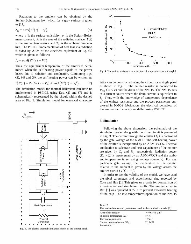
Ž .Fig. 4. The emitter resistance as a function of temperature solid triangle .
istics can be constructed using the circuit for a single pixelas shown in Fig. 1. The emitter resistor is connected to
Ž .V s5 V and the drain of the NMOS. The NMOS actsDD
as a current source where the drain current is equivalent toI . Thus, with the knowledge of temperature dependenceB
of the emitter resistance and the process parameters em-ployed in NMOS fabrication, the electrical behaviour ofthe emitter can be easily modelled using PSPICE.
3. Simulation
Following the above discussion, the schematic of thesimulation model along with the drive circuit is presented
Ž .in Fig. 3. The current through the emitter I is controlledB
by the gate voltage of the NMOS. The self-heating powerof the emitter is incorporated by an ABM-VCCS. Thermalconduction to substrate and heat capacitance of the emitterare given by C and R , respectively. Radiation powerT CŽ Ž ..Eq. 6 is represented by an ABM-VCCS and the ambi-ent temperature is set using voltage source V . For any0
particular gate voltage, the temperature of the emitterrelative to the ambient is given by the voltage across the
Ž Ž . .emitter circuit V t yV .o
In order to test the validity of the model, we have usedthe pixel parameters and experimental data reported by
w xCole and Han 1 . This gives us a basis for comparison ofexperimental and simulation results. The emitter array in
w xRef. 1 was operated at 77 K to prevent excessive heatingof the chip. The low temperatures operation of the NMOS
Table 2w xThermal resistance and parameters used in the simulation model 1
2Area of the emitter ;40=40 mmŽ .Substrate temperature T 77 K0
Thermal capacitance 1.7 nFŽ .Conduction to substrate R 2.1 MVC
Emissivity 1

( )S.R. Kiran, G. KarunasirirSensors and Actuators A72 1999 110–114 113
Fig. 5. Plot of emitter temperature as a function of gate voltage. TheŽ . Ž .simulation results solid curve and experimental data solid triangles are
plotted for comparison.
Ž .77 K results in higher threshold voltage and largerw xmobility of carriers 14,15 . The parameters of the NMOS
in our model were selected to match the I–V character-w xistics given in Ref. 1 . The temperature dependence of the
emitter resistance was extracted from the load line given inw xRef. 1 . Fig. 4 shows the experimental data of resistance
as a function of temperature along with a fitted curve usinga second order exponential decay. The temperature depen-dence of resistance is incorporated in Fig. 3 using an ABMvoltage controlled voltage source denoted by ‘emitter resis-tor’. The emitter parameters used in the simulation modelare summarized in Table 2.
Fig. 5 shows the simulated temperature of the emitterfor different gate voltages together with the experimental
w xdata 1 for comparison. It can be seen that at higher gatevoltages the temperature tend to saturate for two reasons:Ž .i at higher current, the voltage drop across the emitterresistance is high enough to the drive the NMOS from
Ž .saturation to the linear region, and ii the exponentialdecay of the emitter resistance as a function of temperatureindicates that at higher temperatures, the change in resis-tance is small. The close agreement of the simulated andexperimental results indicates the accuracy of the model.
Fig. 6. The transient behaviour of the emitter temperature at two gatevoltages.
Fig. 7. Self-heating power, corresponding radiation, and substrate conduc-tion losses as a function of gate voltage.
In addition, we have simulated the transient behaviourŽ .see Fig. 6 of the emitter pixel for various gate voltages tounderstand the speed performance which depends on thethermal time constant. The thermal time constant t , of theemitter pixel is defined as:
CTts . 8Ž .1 1
qR RC R
Typically, t is of the order of a few milliseconds for highefficiency and high frame rate operation of the resistor
w xarray 2 . It is evident from Fig. 6 that the thermal timeconstant of the emitter is about a few milliseconds andwith increasing gate voltage, the time constant is found to
Ž .decrease. Such a behaviour is expected from Eq. 8 due tothe fact that the thermal conductance increases as a resultof higher radiation heat loss. The predicted time constantagrees well with the experimental value of about 5 ms
w xwhen V yV s1.3 V 1 . This implies that the simulationg T
model can also be used to predict the dynamic behaviourof the array. We have also estimated how the input poweris distributed between the radiative and the non-radiativelosses. The increase in emitter temperature is accompaniedby increase in substrate conduction and radiation powerlosses as illustrated in Fig. 7. In the 100–800 K tempera-ture range, the power loss is dominated by the heat con-ductance through the legs of the emitter.
4. Conclusion
A technique to model the electro-thermal behaviour ofmicroemitters in an array is described using analog be-havioural models in PSPICE. We have shown that thismodel can be used to study both electrical and thermalperformance of the emitter at various operating conditions.The simulated behaviour of the emitter is in good agree-

( )S.R. Kiran, G. KarunasirirSensors and Actuators A72 1999 110–114114
ment with the experimental observations. In addition, thetransient behaviour of the emitter can be used to optimisethe speed of operation. The same model is also used toestimate the dissipation of input power through substrateconduction and radiation. The estimated power distributionresults can be used to design optimized emitter resistorsand its thermal interface with the substrate. The versatilityof this simple simulation model is demonstrated by itscapability to predict many pixel properties in the samedesign environment. The possibility of extracting widevariety of parameters with the help of simulation mayresult in better design of emitter configurations to optimizethe performance.
Acknowledgements
The authors would like to thank J. Yu, Y.H. Chee andM.V.S. Ramakrishna for their helpful discussions. Specialthanks to PSPICE customer support for fast and helpfulsuggestions regarding the use of the simulator software.This work is supported in part by NSTB grant GR 6471.
References
w x1 B.E. Cole, C.J. Han, Low Power Infrared Scene Projector Array andMethod of Manufacture, US Patent a5,600,148, 1997.
w x2 B.E. Cole, C.J. Han, R.E. Higashi, J. Ridley, J. Holmen, Monolithic512=512 CMOS microbridge arrays for infrared scene projection,
The 8th International Conference on Solid State Sensors and Actua-tors, and Eurosensors IX, Sweden, 1995, pp. 628–631.
w x3 D.R. Stauffer, B.E. Cole, Thermal scene projectors using microemit-Ž .ters, Optical Engineering 30 1991 1664–1667.
w x4 M. Parameswaran, R. Chung, M. Gaitan, R.B. Johnson, M. Syrzcki,Commercial CMOS Fabricated Integrated Dynamic Thermal SceneSimulator, International Electron Devices Meeting, Washington, DC,Dec. 8–11, 1991, pp. 753–756.
w x5 R.G. Diggers, K. Barnard, E.E. Burroughs, R.G. Deep, O. Williams,Review of infrared scene projector technology—1993, Optical Engi-
Ž .neering 33 1994 2408–2416.w x6 R.A. Wood, Uncooled thermal imaging with monolithic silicon focal
Ž .planes, Proc. SPIE 20 1993 322–329.w x7 A. Tanaka, S. Matsumoto, N. Tsukamoto, S. Itoh, A. Nakazato, Y.
Kumazawa, M. Hijikawa, H. Gotoh, T. Tanaka, N. Teranishi, In-frared focal plane array incorporating silicon IC process compatible
Ž .bolometer, IEEE Trans. Electron Devices 43 1996 1844–1860.w x8 A.A. Samarskii, P.N. Vabishchevich, Computational Heat Transfer,
Wiley, London, 1991.w x9 C. Jansson, U. Ringh, K. Liddiard, Theoretical analysis of pulse bias
heating of resistance bolometer infrared detectors and effectivenessŽ .of bias compensation, SPIE Proc. 2552 1995 644–652.
w x10 J.S. Shie, Y.M. Chen, M. Ou-Yang, C.S. Chou, Characterization andmodelling of metal film microbolometer, Journal of Microelectrome-
Ž .chanical Systems 5 1996 298–306.w x11 N.R. Swart, A. Nathan, Flow-rate micro-sensor modeling and opti-
Ž .mization using SPICE, Sensors and Actuators A 34 1992 109–122.w x12 F.J. Auerbach, G. Meiendres, R. Muller, G.J.E. Scheller, Simulation
of thermal behaviour flow sensors by equivalent electrical circuits,Ž .Sensors and Actuators A 41–42 1994 275–278.
w x13 Microsim, Microsim PSPICE ArD and BasicsqUsers Guide, Mi-crosim, Irvine, CA, 1993.
w x14 H.C. Nathanson, C. Jund, J. Grosvalet, Temperature dependence onapparent threshold voltage of silicon MOS transistors at cryogenic
Ž .temperatures, IEEE Trans. Electron Devices 15 1968 362–368.w x15 C.G. Rogers, MOST’s at cryogenic temperatures, Solid State Elec-
Ž .tronics 11 1968 1079–1091.