electrònica digital temperature measurement...
TRANSCRIPT
Electrònica Digital
Temperature Measurement System
Grup de classe: 1BT5 Grup de treball Nº: 3 Autors: Andreas Eder, Mario Faschang, Christoph Hangweirer and Franz Peter Musil Data: 09.06.2009
Electrònica Digital
Temperature Measurement System
Andreas Eder, Mario Faschang, Christoph Hangweirer and Franz Peter Musil
Temperature Measurement System
Andreas Eder, Mario Faschang, Christoph Hangweirer and Franz Peter Musil

Temperature Measurement System
2
Abstract:
Many methods have been developed for measuring temperature. Most of these rely on measuring some
physical properties of a working material that varies with temperature. So this change has to be
transformed to an electrical signal and afterwards processed to visualize at a 7 segment display.
Table of contents:
1 Introduction and Specification............................................................................ 3
1.1 Introduction ................................................................................................................................ 3
1.2 Specification and bloc diagrams ................................................................................................. 3
2 System design ..................................................................................................... 4
2.1 The Converter / Input Circuit ..................................................................................................... 4
2.2 ADC – Analog Digital Converter ............................................................................................... 6
2.3 Sequential System to Control AD Conversion ........................................................................... 7
2.4 12 bit D-Latch ............................................................................................................................ 9
2.5 Converter Block.......................................................................................................................... 9
2.6 BIN to BCD Converter ............................................................................................................. 10
2.7 Quadruple BCD to 7 Segment Converter ................................................................................. 11
3 Conclusions and Bibliography.......................................................................... 13
3.1 Conclusions .............................................................................................................................. 13
3.2 Bibliography ............................................................................................................................. 13

3
1 Introduction and Specification
1.1 Introduction
We use a PT100 to measure the temperature. Our PT100 has a temperature range from 0°C to 100°C. The
PT100 changes his resistance from 100Ω to 138.5 Ω. For each 1°C the resistance changes his value by 0.4
Ω. This resistance will be changed by the transducer into a voltage range of 0 V to 10 V. Then this
Voltage is converted into Binary values by an AD-Converter. Afterwards the Binary values are
transformed into BCD Code. Then this code is converted to control the 7 segment displays. We use four 7
segment displays to show the temperature with one decimal place.
1.2 Specification and bloc diagrams
The main part of our project is shown above and the inner part you can see in the circuit below.
The detailed description you can read in the following points.
Temperature Measurement System
4
2 System design
2.1 The Converter / Input Circuit
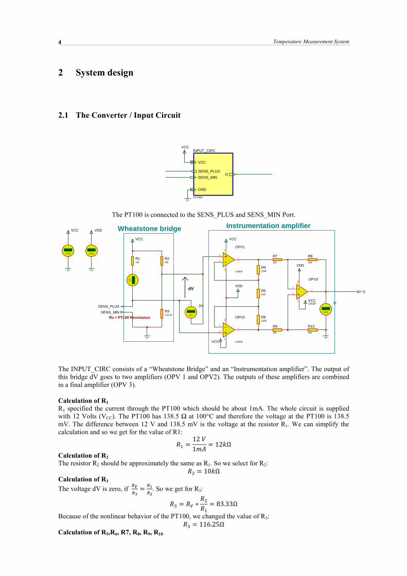
The PT100 is connected to the SENS_PLUS and SENS_MIN Port.
The INPUT_CIRC consists of a “Wheatstone Bridge” and an “Instrumentation amplifier”. The output of
this bridge dV goes to two amplifiers (OPV 1 and OPV2). The outputs of these amplifiers are combined
in a final amplifier (OPV 3).
Calculation of R1
R1 specified the current through the PT100 which should be about 1mA. The whole circuit is supplied
with 12 Volts (VCC). The PT100 has 138.5 Ω at 100°C and therefore the voltage at the PT100 is 138.5
mV. The difference between 12 V and 138.5 mV is the voltage at the resistor R1. We can simplify the
calculation and so we get for the value of R1:
12 1 12Ω
Calculation of R2
The resistor R2 should be approximately the same as R1. So we select for R2:
10Ω
Calculation of R3
The voltage dV is zero, if
. So we get for R3:
83.33Ω
Because of the nonlinear behavior of the PT100, we changed the value of R3:
116.25Ω
Calculation of R5,R6, R7, R8, R9, R10
INPUT_CIRC
CCT006
OSENS_MIN
VCC
GND
SENS_PLUS
VCC
VCC
R112k
R210k
R4220k
R5616
R6220k
R7
10k
R9
10k
R8
10k
R10
10k
+88.8Volts
O
VCC
VCC
VCC
3
21
411
OPV1
LM324
3
21
411
OPV2
LM324
3
21
411
OPV3
LM324
VDD
+88.8
Volts
VCC
+88.8
Volts
VDD
VDD
R3116.25
+88.8
mA
SENS_PLUS
SENS_MIN
O
+88.8
mV
DV
Wheatstone bridge Instrumentation amplifier
dV
Rv = PT100 Resistance
5
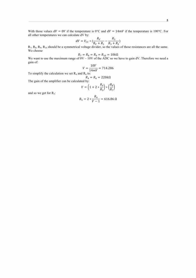
With those values 0 if the temperature is 0°C and 14 if the temperature is 100°C. For
all other temperatures we can calculate dV by:
! R7, R8, R9, R10 should be a symmetrical voltage divider, so the values of those resistances are all the same.
We choose
" # $ % 10Ω
We want to use the maximum range of 0V – 10V of the ADC so we have to gain dV. Therefore we need a
gain of:
1014 714.286
To simplify the calculation we set R4 and R6 to:
' ( 220Ω
The gain of the amplifier can be calculated by:
)1 2 '*
+ )#"
+ and so we get for R5:
* 2 ' 1 616.86 Ω

Temperature Measurement System
6
2.2 ADC – Analog Digital Converter
We use a 12 Bit parallel AD converter AD1674. You can choose between a unipolar and a bipolar input
range. We used the unipolar input range from 0V – 10V.
ADC
CCT007
VIN D[11..0]
CLK
D15
D14
D13
D12
D11
D10
D9
D8
D7
D6
D5
D4
D3
D2
D1
D0
D0
D1
D2
D3
D4
D5
D6
D7
D8
D9
D10
D11
CLK
? ? ? ? ? ? ? ? ? ? ? ? ? ? ? ?
D[11..0]
+88.8Volts
?
12/8 2
CS 3
A0 4
CE 6
R/C 5
REFOUT8
REFIN10
20VIN14
10VIN13
AGND9
STS 28
DB11 27DB10 26
DB9 25DB8 24DB7 23DB6 22DB5 21DB4 20DB3 19DB2
18DB1 17DB0 16VAS
7
VEE
11
BIPOFF12
U1
AD1674
? ? ? ? ? ? ? ? ? ? ? ?VCC
VDD
?
CLK
VIN
?

7
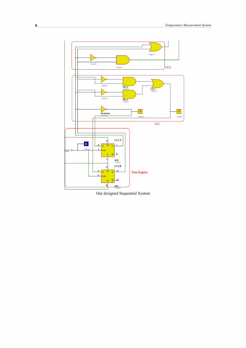
2.3 Sequential System to Control AD Conversion
We designed a sequential system to control the AD Conversion.
When AD is “1” the AD Converter is stared to convert, when DLatch is “1” the D-Latch is set to store the
Data.
The sequential system is controlled by the clock and we use the following truth table for creating the CC1
circuit.
S1 S0 S1
+ S0
+
0 0 0 1
0 1 1 0
1 0 1 1
1 1 0 0
From this we get the expressions: S0+ = S0’
S1+ = S1’ S0 + S1 S0’
For creating CC2 we got the truth table below.
S1 S0 AD DLatch
0 0 0 0
0 1 1 0
1 0 1 1
1 1 1 0
With the expressions: AD = S0 + S1
DLatch = S1 S0’
AD = 0
DLatch = 0
S3
AD = 1
DLatch = 0
AD = 1
DLatch = 1
AD = 1
DLatch = 0
S2
S1
S0
Temperature Measurement System
8
Our designed Sequential System
9
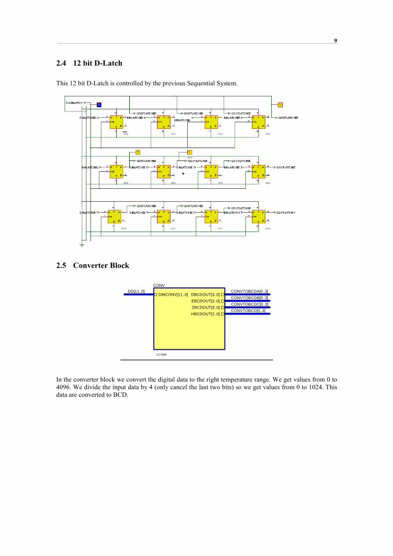
2.4 12 bit D-Latch
This 12 bit D-Latch is controlled by the previous Sequential System.
2.5 Converter Block
In the converter block we convert the digital data to the right temperature range. We get values from 0 to
4096. We divide the input data by 4 (only cancel the last two bits) so we get values from 0 to 1024. This
data are converted to BCD.
CONVTOBCD[0..3]
CONVTOBCDC[0..3]
CONVTOBCDB[0..3]
CONVTOBCDA[0..3]DD[11..0]
CONV
CCT008
DINCONV[11..0]
HBCDOUT[3..0]
ZBCDOUT[3..0]
EBCDOUT[3..0]
DBCDOUT[3..0]

Temperature Measurement System
10
2.6 BIN to BCD Converter
We use this block to convert the binary number to a BCD number. We used the combinational circuit
from the class 2 years before (Exercise 4) http://epsc.upc.edu/projectes/ed/ED/grups_classe/07-08-
q2/1BM2/07-08-Q2-1BM2.htm . Here is also the link to the Proteus file:
http://epsc.upc.edu/projectes/ed/ED/grups_classe/07-08-
q2/1BM2/EX/EX4/est/G7_EX4_Conversor%2016%20bits.DSN
HB
CD
OU
T[3
..0]
EB
CD
OU
T[3
..0]
ZB
CD
OU
T[3
..0] DBCDOUT[3..0]
RE
SIN
BIN
[13.
.0]
RESINBIN9
RESINBIN8
RESINBIN7
RESINBIN6
RESINBIN5
RESINBIN4
RESINBIN3
RESINBIN2
RESINBIN1
RESINBIN10
RESINBIN13
RESINBIN12
RESINBIN11
RESINBIN0
DB
CD
OU
T3
DB
CD
OU
T2
DB
CD
OU
T1
DB
CD
OU
T0
ZB
CD
OU
T0
ZB
CD
OU
T1
ZB
CD
OU
T2
ZB
CD
OU
T3
EB
CD
OU
T3
EB
CD
OU
T2
EB
CD
OU
T1
EB
CD
OU
T0
HB
CD
OU
T0
HB
CD
OU
T1
HB
CD
OU
T2
HB
CD
OU
T3
DINCONV2
DINCONV3
DINCONV4
DINCONV5
DINCONV6
DINCONV7
DINCONV8
DINCONV9
DINCONV10
DINCONV11
DINCONV1
DINCONV0
DBCDOUT[3..0]
EBCDOUT[3..0]
ZBCDOUT[3..0]
HBCDOUT[0..3]
BIN-BCD
BIN-BCD
RES[13..0]
RESTH[3..0]RESH[3..0]
REST[3..0]RESU[3..0]
0 1 1 1 1 0XCVGFHZGNJZUMK
10 0 0
0010
0001
0
00
1
0000
BIN-BCD
BIN-BCD
RES[13..0]
RESTH[3..0]RESH[3..0]
REST[3..0]RESU[3..0]

11
2.7 Quadruple BCD to 7 Segment Converter
The four inputs(BCDINA[0..3], BCDINB[0..3], BCDINC[0..3], BCDIND[0..3]) are each 4-Bit BCD
coded Buses. Each input is for controlling the corresponding “7 segment” display. For this the four
outputs (7segA[0..7], 7segB[0..7], 7segC[0..7], 7segC[0..7]) are used. Each output is a Bus with 8 lines (7
for the segment and one for the dot). The whole display for the temperature consists of four red, 1 digit,
Common Cathode, 7 segment displays.
The inner part of the 4BCD-7SEG is shown below.
RE
ST
H[3
..0]
B[1
3..0
]
RESU1
RESU2
RESU3
REST3
REST0REST1
REST2
RESH3
RESH0
RESH2
RESH1
RESTH0
RESTH2
RESTH3
B0
B1
B2
B3
B4
B5
B6
B7
B8
B9
B10
B11
B12
B13
B14
B15
RESTH1
RESU0
DM74185
CCT003
E
D
C
B
A
Y8
Y7
Y6
Y5
Y4
Y3
Y2
Y1
RES[13..0]
DM74185/2
CCT003
E
D
C
B
A
Y8
Y7
Y6
Y5
Y4
Y3
Y2
Y1
DM74185/4
CCT003
E
D
C
B
A
Y8
Y7
Y6
Y5
Y4
Y3
Y2
Y1
DM74185/3
CCT003
E
D
C
B
A
Y8
Y7
Y6
Y5
Y4
Y3
Y2
Y1
DM74185/6
CCT003
E
D
C
B
A
Y8
Y7
Y6
Y5
Y4
Y3
Y2
Y1
DM74185/5
CCT003
E
D
C
B
A
Y8
Y7
Y6
Y5
Y4
Y3
Y2
Y1
DM74185/9
CCT003
E
D
C
B
A
Y8
Y7
Y6
Y5
Y4
Y3
Y2
Y1
DM74185/8
CCT003
E
D
C
B
A
Y8
Y7
Y6
Y5
Y4
Y3
Y2
Y1
DM74185/7
CCT003
E
D
C
B
A
Y8
Y7
Y6
Y5
Y4
Y3
Y2
Y1
DM74185/12
CCT003
E
D
C
B
A
Y8
Y7
Y6
Y5
Y4
Y3
Y2
Y1
DM74185/11
CCT003
E
D
C
B
A
Y8
Y7
Y6
Y5
Y4
Y3
Y2
Y1
DM74185/10
CCT003
E
D
C
B
A
Y8
Y7
Y6
Y5
Y4
Y3
Y2
Y1
DM74185/15
CCT003
E
D
C
B
A
Y8
Y7
Y6
Y5
Y4
Y3
Y2
Y1
DM74185/14
CCT003
E
D
C
B
A
Y8
Y7
Y6
Y5
Y4
Y3
Y2
Y1
DM74185/13
CCT003
E
D
C
B
A
Y8
Y7
Y6
Y5
Y4
Y3
Y2
Y1
DM74185/16
CCT003
E
D
C
B
A
Y8
Y7
Y6
Y5
Y4
Y3
Y2
Y1
RESU[3..0]
REST[3..0]
RESH[3..0]
RESTH[3..0]
U20
BUFFER
? ? ? ?? ? ? ? ? ? ? ? ? ? ? ?
?

Temperature Measurement System
12
We used the Binary to 7 Segment Circuit from the Electronica Digital Homepage:
http://epsc.upc.edu/projectes/ed/ED/unitats/unitat_2_11/Unitat_2_11.htm
In this circuit a memory is used to control the 7 Segment Display. More Information can be found in the
Web.
The outputs 7SEGA7, 7SEGB7, 7SEGC7, 7SEGD7 are used for displaying the dot in the “7 segments”.
Only the B display needs a dot and so the value of 7SEGB7 is “1”.

13
3 Conclusions and Bibliography
3.1 Conclusions
The Converter / Input circuit has some weak points. If R4, R5, R6 are heated, the resistance will change
and so the gain of the amplifiers will change too and a little error occurs at the output.
To minimize this error, the resistance should be of the same material.
It is really difficult to simulate the whole circuit in Proteus. Often we had a problem with the timing. So
we added a canonical system, which controls the whole conversation process.
3.2 Bibliography
[1] Tietze, Ulrich, “Electronic circuits: handbook for design and application” 2nd ed., Springer
Verlag, 2007
[2] Pàgina web d’Electrònica Digital, Binary to 7 Segment Circuit
http://epsc.upc.edu/projectes/ed/ED/unitats/unitat_2_11/Unitat_2_11.htm
[3] Pàgina web d’Electrònica Digital, BIN to BCD Converter
http://epsc.upc.edu/projectes/ed/ED/grups_classe/07-08-q2/1BM2/07-08-Q2-1BM2.htm