electrical and temperature stress effects on power …
TRANSCRIPT

The Pennsylvania State University
The Graduate School
College of Engineering
ELECTRICAL AND TEMPERATURE STRESS
EFFECTS ON POWER MOSFETS
A Thesis in
Engineering Science and Mechanics
by
Chen Mo
© 2015 Chen Mo
Submitted in Partial Fulfillment
of the Requirements
for the Degree of
Master of Science
May 2015

ii
The thesis of Chen Mo was reviewed and approved* by the following:
Osama O. Awadelkarim
Professor of Engineering Science and Mechanics
Thesis Adviser
Jian Xu
Associate Professor of Engineering Science and Mechanics
Samia A. Suliman
Assistant Professor of Engineering Science and Mechanics
Judith A. Todd
Professor of Engineering Science and Mechanics
Head of the Department of Engineering Science and Mechanics
*Signatures are on file in the Graduate School.

iii
Abstract
High electrical field and high temperature stresses are the two main factors that are critical in
determining power metal-oxide-Si field effect transistor’s (MOSFET’s) reliability and
lifetime. The work reported in this thesis uses planar power n-channel MOSFETs and vertical
U-shaped gated n-channel MOSFETs (UMOSFETs). Electrical stress studies were made on
the planar MOSFETs, whereas the temperature stress studies were performed on the
UMOSFETs. The electrical stress protocols used are those of high voltage application to the
gate at the two opposite polarities as well as hot electron stress. Before and after stress
transistor parameters, including threshold voltage, transconductance, and subthreshold swing
were measured and used to study the stress effects.. The N-channel UMOSFETs were used to
study temperature effects and current stability. A p-n junction of a body diode in the
UMOSFET is utilized and the current-voltage characteristics of the diode are used to provide
data on the temperature of the active region of the UMOSFET. For a constant source-to-drain
current in the UMOSFET the drain-to-source voltage needed to be slightly increased for low
current levels (≤ 500 mA) and decreased for higher current levels.

iv
Table of Contents
List of Figures ....................................................................................................................................... vii
List of Tables .......................................................................................................................................... x
List of Symbols ...................................................................................................................................... xi
ACKNOWLEDGMENT ...................................................................................................................... xiv
Chapter 1 Introduction ............................................................................................................................ 1
1.1 Power Rectifiers ............................................................................................................................ 1
1.2 Power Switches ............................................................................................................................. 2
1.3 Failure Mechanisms of Power Semiconductor Devices ................................................................ 3
Chapter 2 Literature Review ................................................................................................................... 5
2.1 Introduction of MOS Capacitor .................................................................................................... 5
2.2 Operation of MOS Capacitor ........................................................................................................ 6
2.2.1 Flat Band ................................................................................................................................ 7
2.2.2 Depletion ................................................................................................................................ 8
2.2.3 Accumulation ......................................................................................................................... 8
2.2.4 Inversion ................................................................................................................................ 9
2.3 The MOSFET Structure ................................................................................................................ 9
2.3.1 The Planar Structure of MOSFET ....................................................................................... 10
2.3.2 The Vertical Trench MOSFET Structure ............................................................................. 11

v
2.4 Operation of the MOSFET .......................................................................................................... 12
2.4.1 Drain Current versus Gate-to-Source Voltage (ID versus VGS) ............................................ 12
2.4.2 Drain Current versus Drain-Source Voltage (ID versus VDS) ............................................... 15
2.4.3 Threshold Voltage, Transcondance and Subthreshold Slope ............................................... 16
2.5 High Field Transport in Thin Insulators ..................................................................................... 17
2.5.1 Theory of Barrier Tunneling ................................................................................................ 17
Chapter 3 Device Fabrication, Stressing and Characterization ............................................................. 24
3.1 Device Fabrication Process for the UMOSFET .......................................................................... 24
3.2 Device Fabrication Process for Laterally Diffused MOSFETs (LDMOSFET) .......................... 25
3.3 Characterization and Stress Equipment ...................................................................................... 27
Chapter 4 Oxide Stress and Hot Carrier Injection Induced Degradations ............................................ 32
4.1 High Voltage Stress .................................................................................................................... 32
4.1.1 Positive Stress – Negative Stress Sequence ......................................................................... 32
4.1.2 Negative Stress – Positive Stress Sequence ......................................................................... 37
4.2 Hot Carrier Injection ................................................................................................................... 41
4.2.1 Introduction .......................................................................................................................... 41
4.2.2 Types of Hot Carrier Injection ............................................................................................. 41
4.2.3. Experiments and Results ..................................................................................................... 43
4.2.4 Concluding Remarks ............................................................................................................ 50

vi
Chapter 5 Impact of Elevated Temperatures Operation on UMOSFET’s ............................................ 51
5.1 Introduction of Measurement ...................................................................................................... 51
5.2 Temperature Dependence of Body Diode Current Voltage Output ............................................ 52
5.2.1 Circuit Design and Equipment ............................................................................................. 52
5.2.2 Body Diode Forward Bias Output Measurement ................................................................. 53
5.2.3 Discussion of Body Diode IVs ............................................................................................. 54
5.3 Drain Current Stability in the UMOSFET .................................................................................. 56
5.3.1 Experimental Procedure and Results ................................................................................... 57
5.3.2 Discussion ............................................................................................................................ 58
Chapter 6 Conclusion ............................................................................................................................ 68
References ............................................................................................................................................. 71

vii
List of Figures
Figure 1.1: Applications for Power Electronics
Figure 2.1: Schematic of p type substrate MOS capacitor
Figure 2.2: Flat band diagram of aluminum-silicon dioxide-silicon system
Figure 2.3: Cross section of nMOSFET
Figure 2.4: Cross section of n type UMOSFET’s structure
Figure 2.5: Drain Current and Gate-Source Voltage characteristics of an n-type MOSFET
Figure 2.6: Drain Current and Drain-Source Voltage characteristics of an n-type MOSFET
Figure 2.7: Schematic of direct tunneling
Figure 2.8: Schematic of Fowler Nordheim tunneling
Figure 2.9: Numerical analysis of Fowler Nordheim tunneling at t=50nm
Figure 2.10: Numerical analysis of transmission coefficient with respect to oxide thickness
Figure 3.1: SEM micrograph showing the gate oxide on the trench sidewalls and bottom
Figure 3.2: Cross section of laterally diffused MOSFET
Figure 3.3: Model 6000 Test Station
Figure 3.4: A photograph of the two Keithley 238 Source Measurement Units
Figure 3.5: A picture of Keithley 2361 Trigger Controller

viii
Figure 4.1: Cumulative plot of threshold voltage on C2.1
Figure 4.2: Cumulative plot of maximum transconductance on C2.1
Figure 4.3: Cumulative plot of subthreshold slope on C2.1
Figure 4.4: Cumulative plot of threshold voltage on C2.2
Figure 4.5: Cumulative plot of maximum transconductance on C2.2
Figure 4.6: Cumulative plot of subthreshold slope on C2.2
Figure 4.7: Cumulative plot of threshold voltage on C7
Figure 4.8: Cumulative plot of maximum transconductance on C7
Figure 4.9: Cumulative plot of subthreshold slope on C7
Figure 4.10: Cumulative plot of threshold voltage on C8
Figure 4.11: Cumulative plot of maximum transconductance on C8
Figure 4.12: Cumulative plot of subthreshold slope on C8
Figure 5.1: Cross section of n type UMOSFET’s structure
Figure 5.2: Characteristics of forward bias voltage and current in the parasitic body diode,
under specific temperatures ranging from -45 °C to 150 °C (228K to 423K)
Figure 5.3: ln(IDiode) versus forward bias voltage under specific temperature ranging from
-45 °C to 150 °C (228K to 423K)

ix
Figure 5.4: Drain to source voltage versus time, under specific constant drain currents
ranging from 100mA to 2500mA
Figure 5.5: Drain to source voltage versus time with constant current at 100mA
Figure 5.6: Drain to source voltage versus time with constant current at 200mA
Figure 5.7: Drain to source voltage versus time with constant current at 500mA
Figure 5.8: Drain to source voltage versus time with constant current at 1000mA
Figure 5.9: Drain to source voltage versus time with constant current at 1200mA
Figure 5.10: Drain to source voltage versus time with constant current at 1500mA
Figure 5.11: Drain to source voltage versus time with constant current at 2000mA
Figure 5.12: Drain to source voltage versus time with constant current at 2500mA

x
List of Tables
Table 4.1: Device Description on C2.1 and C2.2 (C2.1 is the module of C2 with cellname
NI01, and C2.2 is the module of C2 with cellname NI02)
Table 4.2: Device description on C7
Table 4.3: Device description on C8

xi
List of Symbols
q: Electronic charge
χ: Electronic affinity of silicon
χoxide: Electron affinity of silicon dioxide
Eg: Band gap energy
EC: edge of the conduction energy and of silicon
EV: Edge of the valence energy band of silicon
EF: Fermi energy of silicon
EFM: Fermi energy of the metal
Ee: Electron energy
Eb: Potential energy of the barrier
VFB: Flat band voltage
VGS: Gate-to-source voltage
VDS: Drain-to-source voltage
VDS sat: Drain-to-source saturation voltage
VD: voltage across the diode
VT: Thermal voltage

xii
Vth :Threshold voltage
ΦM: Electric potential of metal
Φox: Silicon-silicon dioxide interface potential barrier for electrons
qΦ: Energy barrier height
εox: Electrical field in the oxide
ID: Drain current
IDiode: Diode current
IB: Reverse bias saturation current
Cox: Oxide capacitance per unit area
CD: Depletion layer capacitance per unit area
CIT: Interface trap capacitance per unit area
g: Transconductance
gm: Maximum transconductance
μn: Electron mobility
μeff
: Effective electron mobility
λ: Channel length modulation parameter
S: Subthreshold swing
KB: Boltzmann constant

xiii
Dit: Interface trap density
JFN: Fowler Nordheim tunneling current density
Jmos : Electron diffusion current density
Jc: Collector current density of the parasitic n-p-n bipolar transistor
h: Planck constant
ħ: Reduced Planck constant
T: Temperature in Kelvin
W: Gate width
L: Gate length
l: Length of the barrier
m*: Effective mass of electron
n: Ideality factor

xiv
ACKNOWLEDGMENT
The accomplishments in this thesis would not have been possible without the support
of many individuals. First, I would like to thank my advisor Dr. Osama Awadelkarim, for his
valuable suggestions and guidance. I would also like to thank Dr Samia Suliman and Dr. Jifa
Hao for many helpful discussions during the course of this work. I am grateful to Fairchild
Semiconductor, Inc. for providing the samples studied in this work and for the provision of
financial support for my summer 2012 internship at Fairchild Semiconductor Inc. laboratories
in Portland, ME.

1
Chapter 1
Introduction
Compared with digital devices in microprocessors, power semiconductor devices are
operated in high power applications, and play an important role in power management [1].
More than 60 percent of all power systems in the USA use at least one set of power
semiconductor devices [1], which helps to use electricity more efficiently. Fig 1 [1] shows a
more detail picture about the applications of power electronics in different blocking voltage
ranges:
Fig 1.1: Applications for Power Electronics

2
The range of operational current is from 0.01 amperes to more than 100 amperes, and the
blocking voltage can span the range from 10 volts to more than 10000 volts. In Fig 1, display
drives are shown to be low current and low voltage applications, whereas devices used in
power supplies and automotive are operated at low voltage but relatively high current. Within
the intermediate current and voltage ranges, 0.1 amperes < Device Current < 100 amperes
and 100 V< Blocking Voltage < 1000V, the applications are telecommunication circuits,
factory automation, motor control and lamp ballasts. The high-end power application shown
in Fig 1 is high voltage direct current electric power transmission system.
Based on their functions, power discrete devices can be categorized into power rectifiers and
power switches [2].
1.1 Power Rectifiers
In low voltage applications, for which blocking voltage is less than 100V, power rectifiers are
either Schottky barrier diodes or p-i-n diodes [2]. A Schottky barrier comprises a
metal-semiconductor junction. In the forward bias mode of operation of a metal-on-n-type
semiconductor Schottky diode the metal acts as the anode side and n-type semiconductor is
the cathode. Compared with schottky diode, p-i-n diode is derived from the traditional p-n
diode, in which an intrinsic semiconductor layer is sandwiched between two oppositely
doped regions. This intrinsic layer is very effective in minimizing the damaging effects of
high electric fields applied to the diode [3]. In high voltage applications with blocking

3
voltages exceeding 100V, p-i-n diodes are most often used [2].
1.2 Power Switches
In low blocking voltage, which is less than 100 volts, and high switching speed with
frequencies larger than 100 kHz [2], power metal oxide silicon field effect transistors
(MOSFETs) are commonly used. In this thesis, U-shape power MOSFETs (UMOSFETs) are
discussed in detail and more discussion of these devices is given in chapter 2. Unfortunately,
when actual stress voltage is high, the power dissipation of power MOSFET is very high [1].
When operating at voltages exceeding 300V, insulated gate bipolar transistors (IGBT) replace
MOSFETs as the main power switches [2]. Insulator gate bipolar transistor has high input
impedance [2], so the bipolar current can be controlled by insulated gate terminal [1].
Another option for high voltage power switches is metal-oxide-semiconductor-gate
controlled thyristor. The structure of a thyristor consists of four layers with alternating P and
N-type materials. Similar to insulated gate bipolar transistors and power metal oxide
semiconductor transistors, gate terminal controls the thryistor’s turn-on and turn-off actions
[2].
1.3 Failure Mechanisms of Power Semiconductor Devices
Stress-induced and thermal induced degradations are two main mechanisms of damage to the
reliability of metal–oxide–semiconductor field-effect transistors. When a large voltage is
applied to a MOSFET, a high electric field develops across the gate dielectric layer causing

4
tunneling problems. Also, high electric field across the channel of the MOSFET causes hot
carrier injection. In addition, a portion of the power consumed by transistors is transformed
into heat, which is stored inside device causing the junction temperature to rise. The
self-heating of power devices causes junction temperature to increase rapidly with respect to
time, and eventually damage the device.
In this thesis, electrical stress-induced degradation mechanisms in power MOSFETs will be
presented and discussed. The thesis will, also, address self-heating in power MOSFETs and
their impact in device performance and reliability.

5
Chapter 2
Literature Review
This chapter provides a background material in the devices fabricated and measured in this
work are power field effect transistors. In the first three sections we will discuss the structure
of a capacitor component of the transistor followed by the discussion of the transistor’s
structure and operation. A major focus of the research presented in this thesis is in the high
electric-field stress of the power transistors. Because of this focus we will also include in this
chapter a discussion of tunneling in thin insulators induced by high electric fields across the
insulator.
2.1 Introduction of MOS Capacitor
The structure of a metal-insulator-semiconductor (MIS) capacitor consists of three layers.
The top layer is metal followed by a dielectric layer in the middle and a semiconductor
substrate at the bottom. The metal part of the MIS is called the gate and the MIS is a two-
terminal, gate and substrate, device structure. The special and most common type of MIS
capacitor is the one in which the metal part may be a highly n-type doped (n+) polycrystalline
silicon, the insulator part is a silicon oxide (oxide), and the semiconductor substrate is silicon.
This capacitor is abbreviated MOS capacitor for metal-oxide-Si. If n type dopants, such as
phosphorus, are added to the Si substrate, the concentration of electrons is larger than that of
holes and the Si is, hence, an n-type Si. In contrast, if p type dopants, such as boron, are

6
added to the Si substrate, holes concentration is larger than the electron concentration and the
Si is p-type Si. Fig 2.1 shows a schematic of MOS capacitor on a p-type substrate [4]:
Fig 2.1 Schematic of p type substrate MOS capacitor
2.2 Operation of MOS Capacitor
There are three operation modes of MOS capacitor: accumulation, depletion and inversion. It
is noted that he discussion of the three operation modes below pertains to a p-type Si

7
substrate. Before we get into the modes of operation we first describe the “flat-band”
condition.
2.2.1 Flat Band
Flat band means that the energy band diagram of semiconductor is flat. Fig 2.2 shows a flat
band diagram of aluminum-silicon dioxide-silicon system [4]:
Fig 2.2: Flat band diagram of aluminum-silicon dioxide-silicon system
In Fig 2.2, EFM is the Fermi energy of the metal, qΦM is the work function of metal, and q is
8
the electronic charge. EF represents the Fermi energy of silicon, and EC and EV are the edges
of the conduction and valence energy bands in silicon. Eg is the band gap energy of silicon.
The electron affinity of the oxide is oxide, and that of silicon is If the oxide and
oxide-silicon interface are ideal, the flat band voltage, which is VFB, equals to the difference
of work function between metal and semiconductor. In reality, however, there are layers of
positive charge in oxide and oxide-semiconductor interface, and it should be removed from
the flat band voltage.
2.2.2 Depletion
It happens when the applied voltage is greater than the flab band voltage but smaller than the
threshold voltage. The majority carriers, which are holes, are diffused to the bulk of
semiconductor away from the oxide/semiconductor interface, and there is a region depleted
from or without any free carriers (holes) inside. This region is called the depletion region. As
larger voltage applied to the gate, the width of depletion region is larger.
2.2.3 Accumulation
Accumulation occurs when the gate voltage is smaller than the flat band voltage, which is
negative in most cases, and holes are attracted from the bulk to the surface of semiconductor.
In this mode, no depletion region is presented.

9
2.2.4 Inversion
Inversion occurs when the applied voltage is greater than a certain value of the gate voltage
called the threshold voltage. Beyond this applied gate voltage the width of the depletion layer
does not increase anymore. At the same time, a layer of electrons is formed near the
oxide-semiconductor interface, and that layer is called the inversion layer.
2.3 The MOSFET Structure
The structure of the metal-oxide-semiconductor (Si) field-effect transistor (MOSFET) is
derived from the MOS capacitor, but there are two more regions that are engineered in the
substrate and integrated to the device. These two regions are highly doped regions with
doping type that is opposite to that of the semiconductor substrate. These regions are called
the source and the drain parts of the MOSFET. The MOSFET is, hence, a four terminals
device: gate, source, drain and substrate. In many applications the source and substrate
terminals may be connected together and as such the MOSFET is sometimes regarded as a
three terminals device. In this thesis, two structures of MOSFET are introduced: the planar
and the vertical trench structures.

10
2.3.1 The Planar Structure of MOSFET
This type of MOSFET is similar to MOS capacitors, but there are two more regions doped as
source and drain in the substrate. The planar MOSFET lies on the plane of the substrate. If p
type substrate is used, regions of source and drain are doped with n type dopants. This type of
device is called n type MOSFET. In contrast, when the source and drain are p+ doped on an
n-type semiconductor substrate the device is called a p type MOSFET. Fig 2.3 shows the
cross section of nMOSFET [4]:
Fig 2.3: Cross section of nMOSFET

11
2.3.2 The Vertical Trench MOSFET Structure
The U-shaped trench-gated MOSFET (UMOSFET) is a vertically oriented device and
constructed along the thickness of the substrate as shown in Fig. 2.4 [5]. The source and drain
of the UMOSFET are located at the top edge and bottom of a U-shaped trench, respectively
[5]. The oxide layer is grown on the sidewalls and base of the trench, whereas the rest of the
trench is filled with the metal gate. The current flow in this structure is vertical from the
source to the drain as compared to the planar MOSFET where the current flows along the
plane of the substrate.
Fig 2.4: Cross section of n type UMOSFET’s structure

12
The body terminal of the device, if it exists, is located on the topside of the device adjacent to
the source. An n type UMOSFET is usually built in a p-type well region implanted on an
epitaxially-grown n-type layer and the opposite is true for a p type UMOFET. The epitaxial
n-type layer is grown on an n+ substrate to facilitate Ohmic contact to the drain.
2.4 Operation of the MOSFET
In order to understand how MOSFET works, it is important to know the relation between
drain current and applied voltages, which are drain-source and gate-source voltages. The
following description is based on an n type enhanced MOSFET.
2.4.1 Drain Current versus Gate-to-Source Voltage (ID versus VGS)
Fig. 2.5 shows the drain current (ID) as a function of the gate-to-source voltage (VGS) at a
constant drain-to-source voltage (VDS).

13
Fig 2.5: Drain Current and Gate-to-Source Voltage characteristics of an n-type MOSFET
One of the functions of transistors is switching. At a small gate voltage the drain current is
very small and almost zero. In this the transistor is in its OFF state. However, when the
gate-source voltage reaches a certain value, called the threshold voltage (Vth) the drain
current starts to show up and increases in value as the gate voltage further increases. The
transistor is then said to be in its ON state. From Fig 2.5, it can be seen that that the threshold
voltage for the device is slightly above 1.5 V. There are three regions of interest in the
MOSFET’s characteristics.

14
Region1: When gate-to-source voltage is smaller than threshold voltage (VGS<Vth), the
MOSFET is in the cut off region. In the cut off region, there is no current in the channel and
device is in OFF state. When VGS is a few tenths of volts below the threshold voltage [3], the
transistor is said to be in the subthreshold region. In this region, the drain current increases
exponentially with the gate voltage [3].
Region 2: When VGS is greater than Vth and drain-to-source voltage is less than VGS – Vth
(VGS > Vth and VDS < ( VGS – Vth )), the MOSFET is in the triode region. In this region, the
MOSFET behavior is like a resistor, and the drain current, is given by [3]:
(2.1)
Where μn is the electron mobility, Cox is the oxide capacitance per unit area, W is the gate
width and L is the gate length.
Region 3: When VGS is greater than Vth and drain-source voltage is greater or equal to VGS –
Vth (When VGS > Vth and VDS ≥ (VGS–Vth ), the MOSFET is in the saturation region. From Fig
2.5, when the device is operated in the saturation region, the drain-to-source voltage does not
influence the drain current anymore. In this region the drain current attains a more or less
steady level. This region is called the saturation region indicating that ID saturates and VDS for
the onset of saturation is written as VDSsat. VDSsat equals to VGS–Vth. The equation of drain
current in this region is given by [3]:
(2.2)

15
λ is the channel-length modulation parameter.
2.4.2 Drain Current versus Drain-Source Voltage (ID versus VDS)
Fig 2.6 is an example of the drain current and drain-to-source voltage characteristics of
n-type MOSFET [4]. These characteristics are drawn for several gate-to-substrate voltages.
Fig 2.6: Drain Current and Drain-to-Source Voltage characteristics of an n-type MOSFET (VTN is
threshold voltage for NMOSFET)

16
The cut off region happens when drain current is zero. When drain current increases with
respect to drain voltage, device works in triode region. The saturation region is reached when
drain current saturates with respect to drain voltage.
2.4.3 Threshold Voltage, Transcondance and Subthreshold Slope
From the ID versus VGS characteristics of the transistor measured at a constant VDS several
transistor parameters can be extracted. These parameters are the threshold voltage, Vth, the
maximum transconductance, gm, and the subthreshold swing, S. Vth is determined from the
tangent to the ID vs VGS curve at the bottom of the linear region and the intersection of this
tangent with the VGS axis.
Conductance is defined as reciprocal of resistance. The transconductance, g, of the transistor
is defined as
g =ΔI𝐷
ΔV𝐺𝑆 (2.3)
The maximum value of this transconductance, gm, is of interest and it is the parameter that is
determined from the ID vs VGS curve. In the subthreshold region, the drain current increases
exponentially with respect to gate voltage. Thus, the logarithmic drain current is linearly
proportional to the gate current, and the slope is called the subthreshold slope, S. The

17
equation for subthreshold slope is [3]:
S =𝑘𝐵𝑇
𝑞𝑙𝑛 (1 +
𝐶𝐷+𝐶𝐼𝑇
𝐶𝑜𝑥) (2.4)
Where CD is depletion layer capacitance per unit area, Cox is oxide capacitance per unit area,
CIT is interface trap capacitance per unit area and 𝑘𝐵𝑇
𝑞 is the thermal voltage (T is
temperature in Kelvin and kB is the Boltzmann constant), which is written as VT.
Subthreshold slope is easy to get from the curve of logarithmic drain current vs gate voltage,
and CD and Cox are known for typical devices. The thermal voltage is 25.85mV at room
temperature. Thus, interface capacitance per can be calculated from the equation, and
interface trap density, which is written as Dit, can also be calculated.
2.5 High Field Transport in Thin Insulators
2.5.1 Theory of Barrier Tunneling
Classical mechanics tells us that an electron is able to “travel” through an energy barrier
lower than the electron energy. In contrast classical mechanics also asserts that an electron is
not able to travel across an energy barrier that is larger than the electron energy. However,
quantum mechanics shows that there is a finite probability that an electron with a lower
energy than an energy barrier is able to travel through the barrier. From quantum mechanics
there are two ways for the electron to travel through the barrier: direct tunneling and variable
range hopping. In this section, direct tunneling, especially the type of tunneling that is called
18
“Fowler-Nordheim” tunneling, will be discussed.
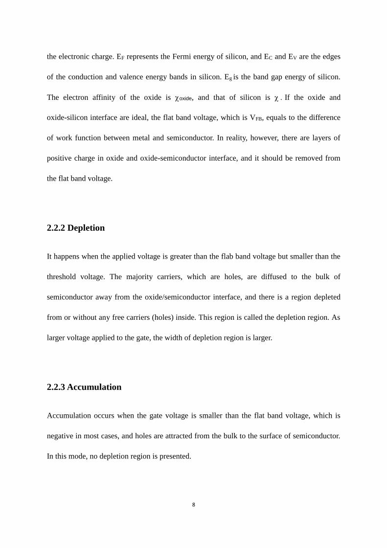
For a MOS system, Si-SiO2 interface energy barrier for electrons is 3.1eV [3]. Using
Schrodinger’s equation to analyze the MOS barrier system, the tunneling coefficient takes the
following form [6]:
Tunneling Coefficient = exp {−2 ∫ √2𝑚
ħ2 (𝐸𝑏(𝑥) − 𝐸𝑒)𝑙
0𝑑𝑥} (2.5)
Where Eb(x) is potential energy of the barrier, ħ is reduced Planck constant, l is the length of
the barrier and Ee is the electron energy. If the electron is tunneling through the whole length
of the barrier, the process is called direct tunneling, which is shown in Fig.2.7 [3].
Fig 2.7: Schematic of direct tunneling

19
For large applied voltage and thin oxide thickness, the electron tunnels only through part of
dielectric length, and this process is called Fowler Nordheim tunneling, which is shown in
Fig 2.8 [3].
Fig 2.8: Schematic of Fowler Nordheim tunneling
Tunneling may generate “defects” within the oxide and oxide/Si interface. These defects may
act as electron traps or hole traps in the bulk oxide or at the oxide/silicon interface [3]. These
defects are very detrimental because they may cause the neutral oxide layer to be charged and,
hence, alter the gate voltages at which the MOS transits between its accumulation, depletion
and inversion modes.

20
Two important parameters, which are current density induced by Fowler Nordheim tunneling
and transmission coefficient are discussed and some mathematical results are given below.
For a simple case, where we assume constant temperature and ignore image force barrier
lowering effects, the tunneling current is given by [7]:
J𝐹𝑁 =𝑞2𝜀𝑜𝑥
2
16𝜋2 ħ𝜙𝑜𝑥 exp (−
4(2𝑞𝑚∗ )0.5𝜙𝑜𝑥 1.5
3ħ𝜀𝑜𝑥2 ) (2.6)
Where JFN is Fowler Nordheim tunneling current density, εox is electric field in the oxide,
𝜙𝑜𝑥 is silicon-silicon dioxide interface potential barrier for electrons, q is electronic charge, ħ
is reduced Plank constant, which equals to Plank constant divided by 2π and m* is effective
mass of electron.
A computer simulation of equation 2.6 is shown in Fig. 2.9. The thickness of the oxide
chosen for the simulation is 50 nm, which is comparable to the gate oxide thickness used in
our devices. Given the oxide data available in the literature we use ϕox = 3.1V. The simulation
is carried out for a gate voltage swept between 0 and 80 V. The results of the simulation for
the FN current are shown in Fig. 2.9 below.

21
Fig 2.9: Numerical analysis of Fowler Nordheim tunneling at t=50nm
From Fig 2.9, the current density is negligible at gate voltages below ~ 60V. However, for
gate voltages above 60V, the current density increases very rapidly. It clearly tells us that only
electrons with enough energy can overcome potential barrier and tunnel into the oxide layer
and, given the gate oxide thickness, the critical electrical field for the onset of large tunneling
current is 1.2*108 V/m. The probability of significant numbers of electrons tunneling below
this critical field is very low and, hence, the tunneling current is almost zero.
We now recall Eq. (2.5) for the tunneling coefficient T and write
Eb(x)-Ee=q-qεx (2.8)

22
Where q is the energy barrier height, and ε is electric field. When x equals to l, the equation
on both side will be zero. Substituting (2.8) in (2.5) and performing the integration yields [3]:
Trasmission Coefficient = exp {−4(2𝑚∗)0.5
3ħ𝑞𝐸(𝑞𝛷)1.5} (2.9)
When Eq. 2.9 is plotted as a function of the insulators thickness for an applied gate voltage of
10 V and for incoming electron energy of 5 V we get the results in Fig. 2.10.
Fig 2.10: Numerical analysis of transmission coefficient with respect to oxide thickness

23
For an electron with energy 5eV to tunnel a barrier of 10 eV, the probability approaches 0
when the tunneling thickness is equal or greater than 10 nm. Thus, it is clear that tunneling
much more pronounced and serious in thin oxides as compares to thick ones. Or tunneling
can also be appreciable in thicker oxides provided the base of the triangular Fowler Nordheim
barrier is thin enough.

24
Chapter 3
Device Fabrication, Stressing and Characterization
3.1 Device Fabrication Process for the UMOSFET
The n-channel UMOSFET (n-UMOSFET) fabrication sequence starts with heavily As-doped
(>1019 cm-3) n+ Si substrate [5] on which an epitaxial layer of phosphorus doped n-type Si is
grown on top of the n+ substrate. The phosphorus doping in the epitaxial layer is ∼ 1016 cm−3
[5]. A p-well is formed in the eoitaxial n-layer using boron implantation to a concentration
of 1017 cm-3 [5]. U-shaped trenches are then reactive-ion etched (RIE) using a commercial
etching tool [5]. Following the trench etching step, a 300 Å sacrificial silicon oxide layer is
thermally grown on the trench side walls at temperatures between 900 and 1000 ºC . The
grown oxide is then wet etched using buffer HF in order to clean the trench surfaces and
eliminate the damage caused by the harsh RIE trench etching [5]. After the cleaning step,
a∼60 nm gate oxide is thermally grown with dry O2 at ~ 1000 °C on the side walls and
bottom of the trench. Poly-silicon is then deposited to fill the trench and in-situ doped with
phosphorous to form the n+ gate electrode. To complete the fabrication process phosphorous
implantation is used to form the n+ source region.
Fig. 3.1 shows a SEM micrograph of the trench in which the gate oxide over the trench
sidewall and bottom are shown [5]. The figure shows that the oxide thickness is somewhat
non-uniform and tends to be thinner at the trench corners and bottom.

25
Fig 3.1: SEM micrograph showing the gate oxide on the trench sidewalls and bottom
3.2 Device Fabrication Process for Laterally Diffused MOSFETs
(LDMOSFET)
In addition to the UMOSFETs, another type of power MOSFET is studied in this work. The
second type is the laterally diffused MOSFET (LDMOSFET), which is schematically shown
in Fig 3.2 [8]:

26
Fig 3.2: cross section of laterally diffused MOSFET
These devices are high voltage LNDMOSFET processed [8] with a 0.5μm dual-gate
bipolar-CMOS-DMOS (BCD) technology [8]. The gate oxide thickness is 60 nm [8]. The full
device processing steps are propriety of Fairchild Semiconductor, Inc., and some limited
details are given in ref. 8.
27
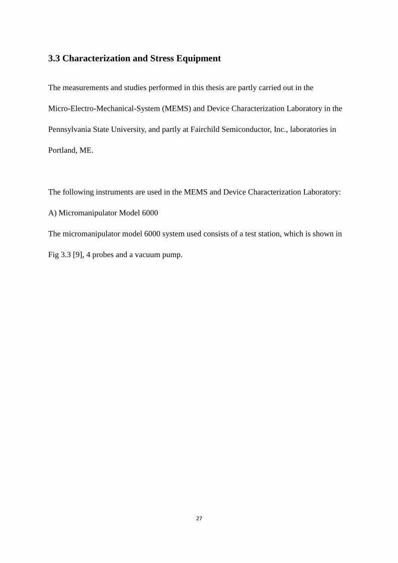
3.3 Characterization and Stress Equipment
The measurements and studies performed in this thesis are partly carried out in the
Micro-Electro-Mechanical-System (MEMS) and Device Characterization Laboratory in the
Pennsylvania State University, and partly at Fairchild Semiconductor, Inc., laboratories in
Portland, ME.
The following instruments are used in the MEMS and Device Characterization Laboratory:
A) Micromanipulator Model 6000
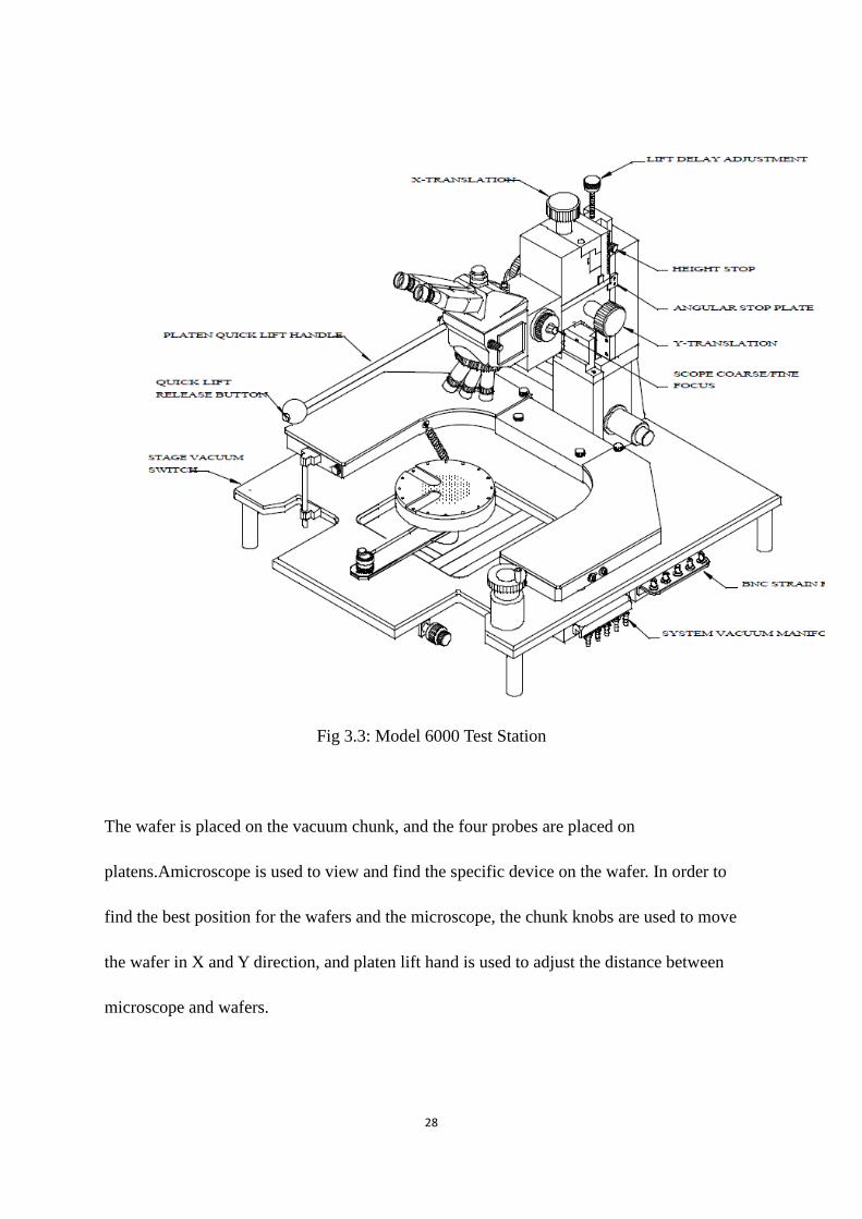
The micromanipulator model 6000 system used consists of a test station, which is shown in
Fig 3.3 [9], 4 probes and a vacuum pump.
28
Fig 3.3: Model 6000 Test Station
The wafer is placed on the vacuum chunk, and the four probes are placed on
platens.Amicroscope is used to view and find the specific device on the wafer. In order to
find the best position for the wafers and the microscope, the chunk knobs are used to move
the wafer in X and Y direction, and platen lift hand is used to adjust the distance between
microscope and wafers.
29
B) Keithley 238 Source-Measurement Units (SMUs)
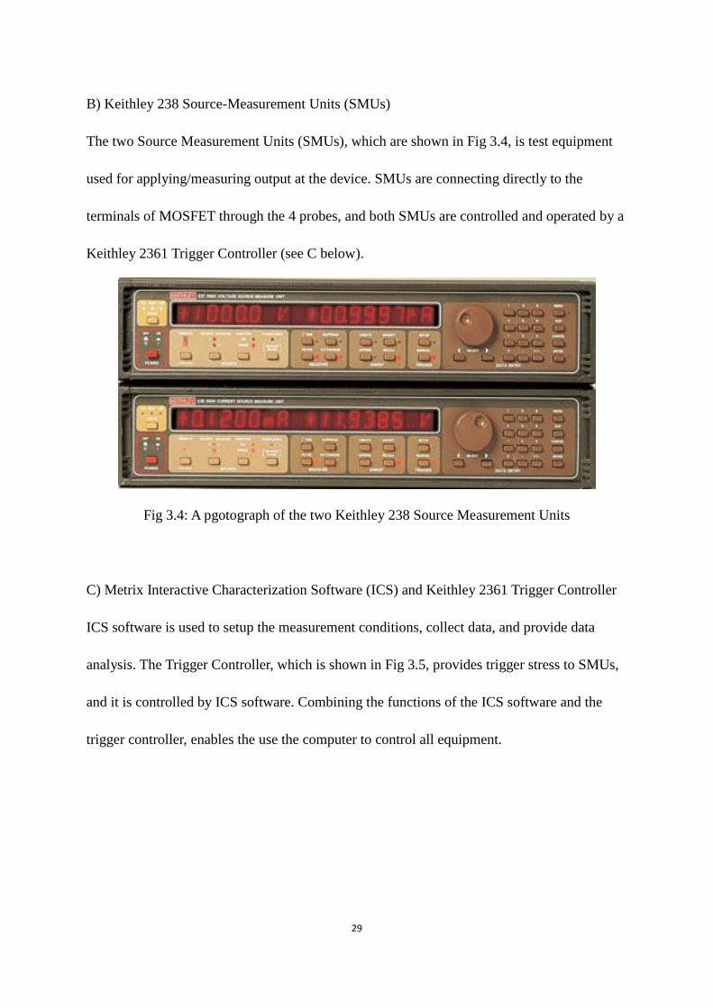
The two Source Measurement Units (SMUs), which are shown in Fig 3.4, is test equipment
used for applying/measuring output at the device. SMUs are connecting directly to the
terminals of MOSFET through the 4 probes, and both SMUs are controlled and operated by a
Keithley 2361 Trigger Controller (see C below).
Fig 3.4: A pgotograph of the two Keithley 238 Source Measurement Units
C) Metrix Interactive Characterization Software (ICS) and Keithley 2361 Trigger Controller
ICS software is used to setup the measurement conditions, collect data, and provide data
analysis. The Trigger Controller, which is shown in Fig 3.5, provides trigger stress to SMUs,
and it is controlled by ICS software. Combining the functions of the ICS software and the
trigger controller, enables the use the computer to control all equipment.

30
Fig 3.5: a picture of Keithley 2361 Trigger Controller
The following instruments are used in Fairchild Semiconductor, Inc,, laboratories at Portland,
ME:
D) KEITHLEY Source Measurement Units (SMUs)
SMUs similar to the ones in B above are used. The SMUs are directly connectied to the
terminals of the MOSFET and are controlled by a B1505A Power Device Analyzer / Curve
Tracer.
E) 34401A Digital Multimeter, 6½ Digit
The Digital Multimeter is used for measuring the output parameters of the device, such as
current, voltage and resistance. The difference of this type of multimeter from the regular
ones is that it can measure alternating current (AC) signals too. In the experimental setup it
is connected directly to the B1505A Power Device Analyzer / Curve Tracer.

31
F) B1505A Power Device Analyzer / Curve Tracer
B1505A Power Device Analyzer / Curve Tracer is the box machine with capability to
characterize high power devices and detect device faults with a curve tracer. In the work
reported in this thesis, B1505A is used for experiment’s setup and to control the SMUs,
which are connected directly to the terminals of MOSFET. In addition, B1505A is used for
collecting data for each experiment from the digital multimeter and plotting it into graphs.
G) 8114A High Power Pulse Generator, 100 V / 2 A
The 8114A High Power Pulse Generator is used for pulse stress of MOSFETs, and it is
connected to the gate terminal of the MOSFET. The 100 V in the equipment label means the
maximum value for the amplitude of the pulse voltage and 2 A refers to the maximum
allowable current.
H) Temperature Forcing Machine
The Temperature Forcing Machine is used to force the environment temperature of the device
to be at the desired value. This equipment consists of the body machine and a long tube. The
tested MOSFET is attached to a plate with tapes and a round shaped rubber with a hole in the
middle that covers the device. The long tube is placed on top of the rubber, and the thermal
couple is placed near the device. It is necessary to make sure that there is inlet to let air in.
The equipment allows for setting the desired temperature and the soak time.

32
Chapter 4
Oxide Stress and Hot Carrier Injection Induced Degradations
4.1 High Voltage Stress
High voltage stress is a condition whereby the thin gate oxide in the MOSFET is subjected to
a high voltage that causes an electric field of the order of 106 V/cm [3]. The purpose of this
measurement is to test the effects of high electrical oxide field on device performance and
predict on device lifetime. One important aspect of this study is to examine possibilities of
eliminating MOSFET’s parameter degradation using some type of a counter stress that
induces charge injection. The experiments described here involve the application of two
electrical stress protocols applied through the gate with the drain and source terminals
grounded.
4.1.1 Positive Stress – Negative Stress Sequence
The descriptions of devices used in the high voltage stress are listed in Table 4.1bellow:
Module Cellname Test device type Device Description
C2 NI01 MOSFET Nch-ISO-01 W=0.5um L=0.8um 5V ISO LVNMOS
C2 NI02 MOSFET Nch-ISO-02 W=25um L=0.8um 5V ISO LVNMOS
Table 4.1: Device Description on C2.1 and C2.2 (C2.1 is the module of C2 with cellname NI01, and
C2.2 is the module of C2 with cellname NI02)

33
These devices are planar MOSFETs with a gate oxide thickness of ~ 600 Å. During the high
voltage stress the drain, source, and substrate terminals are grounded and a +15 V is applied
to the gate for a given period of time. Following the application of this positive voltage stress
the device parameters are measured to monitor device degradation by the stress. Following
this stress another smaller stress with opposite polarity is applied for a shorter duration. The
purpose of this stress is to see whether any recovery on device parameters could be induced
by carrier injection. The results for the measurement of C2.1 are shown in Figures 4.1, 4.2
and 4.3, and the experimental conditions are written in the figure.
Figure 4.1: Cumulative plot of threshold voltage on C2.1
0
20
40
60
80
100
120
0 0.5 1 1.5 2 2.5 3 3.5
%
Vth(V)
Cumulative plot-VthC2.1
before stress
step1:after 15V for 60s
step2:after-10V for 10s
step3:after -10V for 20s

34
Figure 4.2: Cumulative plot of maximum transconductance on C2.1
0
20
40
60
80
100
120
0.00E+005.00E-06 1.00E-05 1.50E-05 2.00E-05 2.50E-05 3.00E-05 3.50E-05 4.00E-05
%
GM(S)
Cumulative plot-max gmC2.1
before stress
step1:after 15V for 60s
step2:after -10V for 10s
step3:after -10V for 20s

35
Figure 4.3: Cumulative plot of subthreshold slope on C2.1
0
20
40
60
80
100
120
0 100 200 300 400 500
%
slope(mV/decade)
Cumulative plot-subthreshold slopeC2.1
before stress
step1:after 15V for 60s
step2:after -10V for 10s
step3:after -10V for 20s

36
From Figure 4.1, the curve of threshold voltage shifts to the right side after +15 V oxide
stress and it moves back to the original position after the -10 V 10 s stress (recovery stress).
However, Fig 4.1 shows that the maximum transconductance decreases after +15V oxide
stress and it does not improve after the recovery stress. The same thing happens to the
subthresold slope.
The positive shift in Vth after the positive stress indicates that negative charge buildup takes
place in the bulk gate oxide. This negative charge buildup may result from negatively charged
defect creation by the high electric field across the oxide, or the ionization (negative charging
due to electron capture) of existing oxide traps by the electrons leaking through the oxide
from the inverted near interface Si. Upon the application of the recovery stress Vth returns
back to its pre-stress value. This is an indication of negative charge
neutralization/compensation in the bulk oxide. It is unlikely that the defects are healed by the
recovery stress but it is tentatively suggested that the negative charge in the oxide is
neutralized. Neutralization may occur due to hole injection in the oxide from the accumulated
near interface Si surface on the negative bias application to the gate.
It is seen that the maximum transconductance (gm) and subthreshold slope (S) are degraded
and remained degraded after both types of stresses. Degradation of gm and S are indicators of
damaged interface. Interface degradation is due to interface trap creation by the stress, which
appears to be unrecoverable by changing stress polarity.

37
4.1.2 Negative Stress – Positive Stress Sequence
In a separate experiment the sequence of stressing is reversed; a negative voltage of -15 V is
applied to the gate of the MOSFET for 60 s with the drain, source and substrate grounded,
followed by a +10 V stress applied at the gate for 10 s and 20 s with the drain, source and
substrate grounded. Measurements of transistor parameters were taken before and after each
stress application. The results for the measurement on C2.2 are shown in Figures 4.4, 4.5 and
4.6, and the experimental conditions are given in the figures.
Figure 4.4: Cumulative plot of threshold voltage on C2.2
0
20
40
60
80
100
120
-2 -1 0 1 2 3 4
%
Vth(V)
Cumulative plot for VthC2.2
before stress
step1:after -15V for 60s
step2:after 10V for 10s
step3:after 10V for 20s

38
Figure 4.5: Cumulative plot of maximum transconductance on C2.2
0
20
40
60
80
100
120
0.00E+00 5.00E-04 1.00E-03 1.50E-03 2.00E-03
%
GM(S)
Cumulative plot-max gmC2.2
before stress
step1:after -15V for 60s
step2:after 10V for 10s
step3:after 10V for 20s

39
Figure 4.6: Cumulative plot of subthreshold slope on C2.2
0
20
40
60
80
100
120
0 200 400 600 800 1000 1200 1400 1600
%
slope(mV/decade)
Cumulative plot-subthreshold slopeC2.2
before stress
step1:after -15V for 60s
step2:after 10V for 10s
step3:after 10V for 20s
40
From Figure 4.4, the threshold voltage shifts to lower voltages after the negative stress, and it
shifts to voltages higher than its pre-stress values. Figure 4.5 shows degradation of maximum
transconductance after first negative stress and it does not improve after the positive
following stress. The subthreshold slope after degrading with the first negative stress
improved slightly after the positive stress but has not fully recovered to the pre-stress value.
In this stress sequence the bulk gate oxide sustains a positive charge buildup after the initial
-15 V stress. With this biasing condition the Si surface near the oxide/Si interface is
accumulated and the hole injection deep into the oxide is enhanced. This hole injection
neutralizes negatively charged oxide traps as well as positively ionizes defects. In both cases
a positive charge buildup occurs giving rise to the negative Vth shift.
Upon the application of the second +10 V stress electrons are injected into the bulk gate
oxide from the inverted Si near the oxide/Si interface. This process induces negative charge
buildup and, thus, the positive shift in Vth. It is not possible to claim recovery with this
positive-voltage stress as the resulting Vth is higher than the pre-stress value. The behavior in
gm and S in this stress sequence is similar to that discussed in 4.1.1. The implication is that
the interface is damaged with the first stress and the damage is not recoverable by stress of
opposite polarity.
Injection of electrons/holes from the Si side of the bulk gate oxide seems to explain the

41
observed behavior in Vth. Also, the injection direction that is consistent with observations and
stress polarity is from the Si side of the MOSFET. It is noted that shifts in all transistor
parameters saturate after a certain stress and no further charge buildup or interface damage
occur in the device.
4.2 Hot Carrier Injection
4.2.1 Introduction
Consider a NMOSFET with gate voltage higher than threshold voltage. The carriers in the
channel, which are electrons, gain enough energy from electrical field in the space charge
region, and they become hot: this is especially the case when the drain-to-source voltage is
high [3]. The hot carriers overcome the potential barrier at the oxide/Si interface and get
injected into the bulk oxide and interface. The energetic carriers transfer energy to other
carriers, and cause them to become hot [3]. From numerous experiments and analysis, most
of the hot carrier injection happens near to drain [3], and that is where damage to the device
takes place. Compared with the majority carriers in the NMOSFET (electrons), the carriers in
the PMOSFET (holes) have heavier weights and less mobility. Thus, hot carrier injection
affects more pronounced in NMOS rather than in PMOS [14].
4.2.2 Types of Hot Carrier Injection
The classification of hot carrier injection depends on the injection mechanisms, and there are
four types of mechanisms [10][11].

42
The first type of injection is called Channel Hot-Electron Injection [10]. When gate voltage
approximately equal to drain voltage, the effect of channel hot carrier is at maximum [10]. In
this case, high gate voltage attracts electrons and causes them to overcome potential barrier
between Si and SiO2 near drain end [10]. If gate voltage is too low, the energy from electrical
field is not enough to attract electrons [10]. In contrast, when gate voltage is much higher
than drain voltage, avalanche multiplication due to impact ionization [10] happens, so gate
voltage is not the only source to cause carrier injection.
The second type of injection mechanism is called Drain Avalanche Hot-Carrier Injection [10].
It mainly happens when higher drain voltage and lower gate voltage are applied [11]. This is
the case discussed in the introduction section, and measurements in this work are focused on
this type of carrier injection.
The third type of injection mechanism is called Secondarily Generated Hot-Electron Injection
[12] [13]. This happens when high electrical field is applied in the channel, photons are
generated near drain end [10], and they induce the generation of electron-hole pairs [10]. In
addition, impact ionization also happens in this mechanism [10].
The fourth type of injection mechanism is called Substrate Hot-Electron/Hole Injection [11].
The carriers, either electrons or holes, get enough energy from high bulk voltage [10]. The
injection mechanism is similar to previous three types of injection.

43
4.2.3. Experiments and Results
The device description of the planar MOSFETs used is given in Table 4.2 and Table 4.3:
Module Cell Name Test Device Device Description
C7 NI05 MOSFET Nch-ISO-05 W=25um L=0.8um 3 stripes 5V ISO LVNMOS
Table 4.2: Device description on C7
Module Cellname Test device type Device Description
C8 NTG06 MOSFET Nch-TG-06 W=25um L=0.5um 5 stripes Thick
Gate NMOS
Table 4.3: Device description on C8
The results for the measurement of C2.7 are shown in Figures 4.7, 4.8 and 4.9, and the
experimental conditions are written in the figures.

44
Figure 4.7: Cumulative plot of threshold voltage on C7
0
20
40
60
80
100
120
0 0.5 1 1.5
%
Vth(V)
Cumulative plot of VthC7
before stress
after VG=5V,VD=3V,t=60s
after VG=5V,VD=8V,t=60s
after VG=5V,VD=12V,t=60s

45
Figure 4.8: Cumulative plot of maximum transconductance on C7
0
20
40
60
80
100
120
0 2 4 6 8 10 12 14
%
gm(10^-3)
Cumulative plot of maxmium gmC7
before stress
after VG=5V,VD=3V,t=60s
after VG=5V,VD=8V,t=60s
after VG=5V,VD=12V,t=60s

46
Figure 4.9: Cumulative plot of subthreshold slope on C7
From Fig.4.7, hot carrier injection does not affect threshold voltage, and it means that the
quality of oxide bulk does not degrade, in terms of charge buildup, after stressing. However,
maximum transconductance begins to degrade after second stress, followed by a large
decrease in gm after the last stress. This large degradation in gm after the third stress is
accompanied by a large increase subthrehold slope.
0
20
40
60
80
100
120
1 10 100 1000 10000
%
slope(mV/decade)
Cumulative plot of subthrehsold slopeC7
before stress
after VG=5V,VD=3V,t=60s
after VG=5V,VD=8V,t=60s
after VG=5V,VD=12V,t=60s

47
The results for the measurement on C2.8 devices are shown in Figures 4.10, 4.11 and 4.12,
and the experimental conditions are given in the figures.
Figure 4.10: Cumulative plot of threshold voltage on C8
0.00E+00
2.00E+01
4.00E+01
6.00E+01
8.00E+01
1.00E+02
1.20E+02
0 0.5 1 1.5 2 2.5 3
%
Vth(V)
Cumulative plot-VthC8
before stress
Step1: VG=5V,VD=8V,t=60s
Step2: VG=-10V,VD=0V,t=20s
Step3:VG=10V,VD=0V,t=20s

48
Figure 4.11: Cumulative plot of maximum transconductance on C8
0.00E+00
2.00E+01
4.00E+01
6.00E+01
8.00E+01
1.00E+02
1.20E+02
0.00E+00 1.00E-03 2.00E-03 3.00E-03 4.00E-03
%
GM(S)
Cumulative plot-max gmC8
before stress
step1: VG=5V,VD=8V,t=60s
step2: VG=-1V,VD=0V,t=20s
step3:VG=10V,VD=0V,t=20s

49
Figure 4.12: Cumulative plot of subthreshold slope on C8
This measurement tests the hot carrier effect to the devices and whether a high voltage stress
causes a recovery on device parameters following hot carrier injection. From the results, the
threshold voltage shifts to higher values after the hot carrier injection stress, and it does not
recover after the application of high voltage oxide stress, irrespective of the stress polarity.
Similar observations and conclusions are made on transconductance and subtrehsold slope.
0
20
40
60
80
100
120
1 10 100 1000 10000 100000 1000000
%
slope(mV/decade)
Cumulative plot-subthreshold slopeC8
before stress
step1:VG=5V, VD=8V,t=60s
step2: VG=-10V,VD=0V,t=20s
step3:VG=10V,VD=0V,t=20s
50
4.2.4 Concluding Remarks
From the measurement of C7, significant changes of transconductance and interface traps are
shown after hot carrier injection at drain-to-source voltages much higher than the gate voltage
(VDS ≥ VGS). High drain-to-source voltages during the injection give enough energy to the
electrons, and assist them to tunnel into the interface traps. However, both positive high
voltage stress and negative high voltage stress to the bulk oxide do not recover device
parameters to pre-stress values. It is also observed that hot-carrier injection damage saturates
after a given stress level and parameters are no further changed upon the application of more
stress.

51
Chapter 5
Impact of Elevated Temperatures Operation on UMOSFET’s
5.1 Introduction of Measurement
Elevated temperature operation and its impact on UMSOFET performance and reliability
have become a major concern. A large number of devices are damaged because of
temperature-induced degradations. It is necessary to gain more understanding on thermal
instability of devices and exert more efforts on improving it. The focus of this chapter is to
test the behavior of Power MOSFETs, especially the stability of the drain current and applied
voltage at high temperatures.
The types of measurements described in this chapter can be divided into two categories as
follows:
(1) Measurement of the forward bias current-voltage (IV) characteristics of the body diode
formed when the UMOSFET is biased as shown in Figure 5.1 [15]. The objective of this
experiment is to use the IV characteristics to extract the actual temperature of the
UMOSFET.
(2) Measurement of the drain-to-source voltage (VDS) necessary to maintain the
drain-to-source current (ID) at a constant level as a function of time. This measurement is
carried out on the UMOSFET while it is operated in the saturation region at gate-to-source
voltage (VGS) of 5 V.

52
5.2 Temperature Dependence of Body Diode Current Voltage Output
The IV output of the body diode is used to estimate the temperature of the UMOSFET. The
forward current of the p-n body junction between the body contact and the drain contact is
measured as a function of the forward bias between the body and drain. The biasing condition
on the body diode is shown in Figure 5.1 [15]. Note that the source and body contacts are
short-circuited, however no current flows in the n+-p-n or the source-well-drain structure as it
include two p-n diodes connected back to back. The voltage applied to the gate and drain of
the transistor is 0 V and, hence, the transistor is in its “off” state during this measurement. It
is reasonable to treat the transistor as a body diode, because the device is in off state with no
voltage applied to gate terminal.
5.2.1 Circuit Design and Equipment
These measurements are performed at Fairchild Semiconductor, Inc. Laboratories in
Portland, Maine. The circuit of it is relatively simple: a current is applied from the source side
to the drain side while the gate is floating and the drain is grounded. The set-up for this
measurement includes: a temperature forcing machine, a digital multimeter, a 5A source
meter, a device analyzer and a curve tracer, low resistance wires, cables and connectors. The
types of UMOSFETs used in this experiment are labeled by Fairchild Semiconductor, Inc., as
FDPF3860T and FDP047N10. Both of them are packaged n-Channel Power UMOSFETs.
FDPF3860T has a higher current rating than FDP047N10 with lower static drain to source

53
on-resistance. During measurement the body-to-drain voltage is swept between 0V and 1.2 V
and the current in the diode is measured.
The IV measurements are carried out at different temperatures applied to the packaged
UMOSFET. Before measurements one needs to determine the best temperature soak time for
the packaged UMOSFET. It is found out that the packaged device takes some time to reach
the applied temperature. From testing we made on several applied temperatures it is decided
on a temperature soak time of 20 minutes before measuring the IV characteristics of the body
diode. Clearly this stabilized temperature of the packaged device does not mean that the
actual temperature of the device is that of the packaged device. The IV measurement is
intended to find the actual UMOSFET’s temperature given the packaged device temperature,.
5.2.2 Body Diode Forward Bias Output Measurement
The purpose of this measurement is to test the behavior of voltage drop across body diode at
different temperatures. Two types of power MOSFET are tested at 10 temperatures ranging
from -45 degree to 150 degree. For sample 3 of FD3860T, a measurement of 200 degree is
added to the list. The first step is to use the temperature control machine to set the desired
temperature for 20 minutes, which is found to be suitable by other measurements. During
soak time, parameters of the measurement program, such as interval of time and voltage, are
set as designed. The next step is to process measurements and to transfer data to excel file for
curve plotting. The results of these measurements are shown in Figure 5.2.
54
From Figure 5.2 one can make the following observations:
(1) The turn-on voltage of the body diode shifts to lower applied forward bias with increasing
temperature.
(2) In the linear region of the characteristics the slopes of the IV curves appear to be the same,
i. e., the plots appear to be parallel to one another. Since the slopes of the curves are the same
in the linear region the body diode seems to maintain its on-resistance with variable
temperature.
It is important to consider possible sources of error in this measurement. The main source of
error in the experiment is the stabilization of the applied temperature to the packaged device.
The temperature application system is controlled by a thermocouple, which can sense
temperature around the packaged device and make adjustment to the current applied to the
resistor heater. This process works very well for low temperatures, but it is less reliable for
temperatures above 100 degree. The reason for this is that when the thermocouple is operated
for a long time at high temperatures the two materials from which it is made undergo a shape
change and that gives a higher temperature reading than is actually the case.
5.2.3 Discussion of Body Diode IVs
We start from the diode-voltage equation and discuss how to extract temperature
measurements from this equation. The current for an “ideal” p-n junction can be written as:
Idiode=IB(eqVD/nVT-1)≈IB(eqVD/nKBT) (5.1)

55
where Idiode is the diode current, IB is reverse bias saturation current, VD is the voltage across
the diode, VT is the thermal voltage, n is the ideality factor, q is electronic charge and KB is
Boltzmann constant. The next step is to take natural logarithm, which is ln, on both sides, and
we can get the following equation:
ln(Idiode)=qVD/nkT+ln (IB)=(q/nKBT)VD+C (5.2)
where C is ln(IB), e equals to 1 and k equals to 8.62x10⁻⁵ eV /K. Thus, from the curve of
ln(Idiode) versus VD, it should be possible to calculate the temperature T from the slope of the
curve.
However, Figure 5.3 shows the characteristic of our body diode. It can be seen that the IV
behavior of our p-n junction body diode is not ideal because the curves in each temperature
are not straight before the saturation. The reason is that current has different mechanisms in
different ranges and the ideality factor n is not unity and will take different values at different
voltage regions.
Drain current consists of two parts: recombination current and diffusion current. When p-n
junction is in forward bias condition, electrons in from n region will flow to the p area and
become the minority carriers. Similarly, holes will be the minority carriers in the n region.
However, there is a possibility that holes and electrons will flow to the space charge region
and recombine together. After recombination, the particles will be neutralized and stop to
move. Thus, more current is needed to compensate this loss in the number of carriers, and
this additional current is called “recombination current”. The minority carrier concentration
is also not distributed uniformly in the region. In the edge of the space charge region, the

56
minority carrier concentration is highest, and it will decrease as it moves into the bulk. Thus,
the holes or electrons with high concentration will move into the lower concentration and the
movement of carrier charges is called “diffusion current”.
For the p-n junction, the diode current is dominated by recombination current in the low
applied voltage range and the ideality factor is around 2. For the high applied voltage range,
the diode current is dominated by diffusion current and the ideality factor is near 1. The space
between those 2 regions is called transition region and value of ideality factor is between 1
and 2. Due to the variability of n, it is difficult to get accurate value of actual temperature in
the junction and more measurements are needed.
Even though this method is not perfect, it provides a way to detect the junction temperature
by detecting the forward bias current due to the parasitic body diode. If we can find the
accurate mean ideality factor throughout the whole voltage range, we can easily get the
junction temperature from the discussed equations.
5.3 Drain Current Stability in the UMOSFET
The experiments discussed in this section are focused on studying current stability in the
UMOSFET for different drain-to-source (ID) current levels. In these experiments the
UMOSFET is turned “on” and is operated in the saturation region. The voltage applied at the
gate during these experiments is kept constant at 5 V which is well above the threshold
voltage on the UMOSFET which is ~ 1.5 V. The assumption here is that the UMOSFET gets

57
heated and the temperature of the device increases. As the temperature increases the
drain-to-source voltage (VDS) necessary to keep steady constant ID is expected to change.
5.3.1 Experimental Procedure and Results
There are three different circuits designed for these experiments: (i) applying a constant
voltage through a resistor which is connected in series with the drain and measuring ID; ii)
connecting a current source which supplies a constant ID and measuring VDS; and (iii)
applying a constant drain-to-source voltage and measuring ID without the inclusion of a
resistor.
In the second measurement type and when applying constant ID two source meters are
needed: one of them is to apply constant voltage, which is greater than threshold voltage and
the other is to let constant current flow through the drain to the source terminal, which is
grounded.
The different types of experiments showed that to keep the same ID flowing through the
UMOSFET it is necessary to adjust VDS as time progresses. Similarly to maintain the same
VDS across the UMOSFET one has to adjust ID as time progresses.
Figure 5.4 gives the variation of VDS with time needed to maintain constant ID. It can be seen
from the figure that at low ID VDS stays constant as a function of time for the first 60 seconds.
This is not the case for high ID currents at or higher than 1.5 A. To examine the variation of

58
VDS with time, Figs. 5.5 through 5.12 show the initial short-time variation or VDS. From these
figures one can make the following observations:
(1) In all case VDS varies with time in order to maintain a constant ID in the UMOSFET.
(2) The variation of VDS with time for low currents < 500 mA is in such a way as VDS
increases with time, and the increase in VDS is very small and less than 1%.
(3) For ID levels at or higher than 1 A VDS decreases with time in order to maintain the
constant high ID. The increase is very small at ID below 1.5 A and is below 15%.
(3) At high ID values of 2A and above a very large decrease in VDS is necessary to maintain a
constant ID. The change in VDS may reach up to 75% in these cases.
(5) Changes in VDS, whether an increase or decrease occurs very fast in the first few seconds
and levels off at longer times.
5.3.2 Discussion
In Semiconductor devices, especially for power MOSFET, an increasing temperature will
cause current to be higher, which will induce the temperature to increase at a faster rate. That
is the basic mechanism for “thermal runaway”. According to Dibra etal [16] that drain
current in the saturation region of the UMOSFET results from two components: Imos and Ic.
The equation for Jmos, which is electron diffusion current density, is the following [17]:
59
(5.3)
Where α =1.74, μeff
is the effective electron mobility, K is a constant accounting for the gate
oxide capacitance per unit area, VTh
is threshold voltage and Jmos
has negative temperature
coefficient. Therefore Jmos
decreases with increasing temperature [16].
There are two main parts for Jc, which is the collector current density of the parasitic n-p-n
bipolar transistor: The first part is the electron diffusion current due to electron injected from
the emitter into the base-collector junction of the parasitic n-p-n bipolar transistors. The
second part of the current is the reverse current of the base-collector p-n junction due to the
electron-hole generation in the base-collector junction. The equation for Jc is the following
[16]:
(5.4)
Both currents have positive temperature coefficients, so collector current density increases
with temperature [16].
Combining the observation of Figs. 5.5 through 5.12 and the characteristics of currents
discussed above, it is reasonable to make a conclusion about the mechanism of drain current.
At low current level, drain current has negative temperature coefficient, and it is dominated
by Imos. At higher level of current, drain current has positive temperature coefficient, and it is
dominated by Ic.

60
Figure 5.1: Cross section of n type UMOSFET’s structure

61
Figure 5.2: Characteristics of forward bias voltage and current in the parasitic body diode,
under specific temperatures ranging from -45 °C to 150 °C (228K to 423K)
-2.00E-01
0.00E+00
2.00E-01
4.00E-01
6.00E-01
8.00E-01
1.00E+00
1.20E+00
0 0.2 0.4 0.6 0.8 1 1.2 1.4
Cu
rre
nt(
A)
Voltage(V)
fb voltage of 3860T comparision of 2 samples( sample1 &3)
Is(-45)sample 3
Is(-30)sample 3
Is(-20)sample 3
Is(0)sample 3
Is(25)sample 3
Is(50)sample 3
Is(75)sample 3
Is(100)sample 3
Is(125)sample 3
Is(150)sample 3
Is(-45)sample 1
Is(-30)sample 1
Is(-20)sample 1
Is(0)sample 1
Is(25)sample 1
Is(50)sample 1
Is(75)sample 1

62
Figure 5.3: ln(IDiode) versus forward bias voltage under specific temperature ranging from
-45 °C to 150 °C (228K to 423K)

63
Figure 5.4: Drain to source voltage versus time, under specific constant drain currents
ranging from 100mA to 2500mA
0
0.2
0.4
0.6
0.8
1
1.2
1.4
1.6
1.8
2
0 10 20 30 40 50 60 70
volt
age
(V)
time(s)
VDS vs Time for sample 2
voltage(V)-100mA
voltage(V)-200mA
voltage(V)-500mA
voltage(V)-1000mA
voltage(V)-1200mA
voltage(V)-1500mA
voltage(V)-2000mA
voltage(V)-2500mA

64
Figure 5.5: Drain to source voltage versus time with constant current at 100mA
Figure 5.6: Drain to source voltage versus time with constant current at 200mA
0.00702
0.00703
0.00704
0.00705
0.00706
0.00707
0.00708
0.00709
0.0071
0.00711
0.00712
0 10 20 30 40 50 60 70
Vo
ltag
e(V
)
time(s)
VDS vs Time-100mA
0.01442
0.01444
0.01446
0.01448
0.0145
0.01452
0.01454
0.01456
0.01458
0 10 20 30 40 50 60 70
Vo
ltag
e(V
)
time(s)
VDS vs Time-200mA

65
Figure 5.7: Drain to source voltage versus time with constant current at 500mA
Figure 5.8: Drain to source voltage versus time with constant current at 1000mA
0.03845
0.0385
0.03855
0.0386
0.03865
0.0387
0.03875
0 10 20 30 40 50 60 70
Vo
ltag
e(V
)
time(s)
VDS vs Time-500mA
0.0882
0.0884
0.0886
0.0888
0.089
0.0892
0.0894
0.0896
0.0898
0.09
0.0902
0 10 20 30 40 50 60 70
Vo
ltag
e(V
)
time(s)
VDS vs Time-1000mA

66
Figure 5.9: Drain to source voltage versus time with constant current at 1200mA
Figure 5.10: Drain to source voltage versus time with constant current at 1500mA
0.112
0.1125
0.113
0.1135
0.114
0.1145
0.115
0.1155
0.116
0.1165
0.117
0 10 20 30 40 50 60 70
Vo
ltag
e(V
)
time(s)
VDS vs Time-1200mA
0.15
0.155
0.16
0.165
0.17
0.175
0.18
0 20 40 60 80
Vo
ltag
e(V
)
time(s)
VDS vs Time-1500mA

67
Figure 5.11: Drain to source voltage versus time with constant current at 2000mA
Figure 5.12: Drain to source voltage versus time with constant current at 2500mA
0
0.1
0.2
0.3
0.4
0.5
0.6
0 10 20 30 40 50 60 70
Vo
ltag
e(V
)
time(s)
VDS vs Time-2000mA
0
0.2
0.4
0.6
0.8
1
1.2
1.4
1.6
1.8
2
0 10 20 30 40 50 60 70
Vo
ltag
e(V
)
time(s)
VDS vs Time-2500mA

68
Chapter 6
Conclusion
The first part of the work reported in this thesis focuses on studies of two types of high
electrical stresses on planar MOSFET, one of which is in high voltage oxide stress and the
other one is hot carrier injection. High oxide stress induces damage to bulk dielectric layer
(SiO2) and interface layer. There are two processes happening in the bulk oxide and its
interface with Si during high oxide stress: ionization/charging and bond breaking. Those two
degradation mechanisms result in charge buildup in the bulk oxide and in oxide/Si interface
trap generation. The impact on the MOSFET is manifested as shifts in the threshold voltage
and degradations in the transconductance and in the subthreshold swing. During high voltage
stress defect ionization and charging is observed to dominate in the bulk gate oxide. In the
event of positive voltage stress applied to the gate electrons are injected from the inverted Si
adjacent to the oxide/Si interface deep into the oxide bulk, giving rise to negative charge
buildup. In the interface, however, bonding breaking and charging of dangling bonds
degrades the interface. Positive shift in Vth and decrease and gm coupled with increase in S
are observed. Vth is observed to recover following a negative polarity high voltage stress,
which implies hole injection from the accumulated Si surface during the stress. The injected
holes charge/neutralize defects, which amounts to positive charge buildup and, hence,
recovery in Vth. The reverse polarity stress does not recover either gm or S. A similar scenario
occurs when a first negative high voltage stress is followed by a positive high voltage stress:
the injection sequence is holes from the accumulated Si followed by electrons from the

69
inverted near interface Si. The sequence of Vth shifts is reversed in this case. Changes in gm
and S in this stress sequence are very similar to those occurring the former sequence. The
hot carrier injection is observed to only affect the interface layer, and its impact on the bulk of
the dielectrics is very small. Thus, there is little change on the threshold voltage. No
recoveries in either gm or S are observed following the superposition of high voltage stress on
hot electron stress.
The second part of the work reported in this thesis covers temperature effects on
UMOSFET’s performance and reliability. The first measurement in this part of the work was
to observe the characteristics of a parasitic body diode occurring in a packaged UMOSFET
placed in different environment temperatures when the UMOSFET is OFF. The purpose of
this measurement is to find the actual junction temperature inside the UMOSFET and
compare it to the temperature of the surroundings. It is shown that the body diode
characteristics can be used to measure the actual UMOSFET temperature. However, to
determine the numerical value of the UMOSFET temperature one needs to employ a
reasonable number for the ideality factor of the diode. This can be obtained from the
literature or from the results of an appropriately designed experiment. The second
measurement was to measure the source to drain voltage that maintains a constant drain
current, while the UMOSFET is ON and operated in the saturation region. The reason for this
experiment is to test the temperature effects on the stability of drain-to-source current. Our
results suggest that the UMOSFET exhibits two different mechanisms at different levels of
current. The drain-to-source current has negative temperature coefficient at low current levels

70
and at higher currents above 500 mA, for the device geometries used in this thesis, the current
has positive temperature coefficient. The current component that has a negative temperature
coefficient is the regular MOSFET current in saturation. The current component with the
positive temperature coefficient is a parasitic n-p-n parasitic bipolar junction transistor which
tends to dominate at high current levels.

71
References:
[1] BaligaB.Jayant. (1996). Trends in Power Semiconductor Devices. IEEE Transactions on
Electron Devices,Vol. 43,No 10, 1717-1731.
[2] BaligaB.Jayant. (2001). The Future of Power Semiconductor Device Technology.
Proceedings of the IEEE, Vol. 89, No.6, 822-832.
[3] Ning, Y. T. (2009). Fundamentals of Modern VLSI Devices. Cambridge University Press.
[4] Zegbroeck, b. v. (2011). Principle of Semiconductor Devices. Prentice Hall.
[5] S A Suliman,N Gollagunta, L Trabzon, J Hao, R S Ridley,C M Knoedler, G M Dolny, O O
Awadelkarim and S J FonashN. (2001). The dependence of UMOSFET characteristics and
reliability on geometry and processing. INSTITUTE OF PHYSICS PUBLISHING, 447-454.
[6] SchwablFranz. (2007). Quantum Mechanics. Berlin: Springer.
[7] M.LenzingerE.H.Snow. (1969). Fowler-Nordheim Tunneling into Thermally Grown SiO2.
Journal of Applied Physics, 278-283.
[8] Jifa Hao, Mark Pelletier, Robert Murphy, and Thomas E. Kopley Mark. Self Heating
Effect on Hot Carrier Degradation Characteristic in High Voltage n-channel LDMOS.
[9] Model 6000 Series Test Station Manual
[10] EntnerRobert. (2007). Modeling and Simulation of Negative Bias Temperature
Instability. VDM Verlag .
[11] E.Takedaand T. HagiwaraN.Suzuki. (1983). Device Performance Degradation to
Hot-Carrier Injection at Energies Below the Si-SiO2 Energy Barrier. proc. Intl.Electron
Devices Meeting, 396-399.
72
[12] S. Kohyama, T. Furuyama, S. Mimurat, and H. IizukaT. (1980). Non-Thermal Carrier
Generation in MOS Structures. Jpn.J.Appl.Phys, Vol 19, Supp. 19.1,pp. 85-92.
[13] T.H.Ning. (1978). Hot-Electron Emission from Silicon into Silicon Dioxide. Solid-State
Electron, Vol 21,pp.273-282.
[14] Kueing-Lonb Chen (1985). Reliability Effects on MOS Transistors Due to Hot-Carrier
Injection. IEEE Journal of Solid-state Circuits, Vol. SC-20,No.1.
[15] Gate Charging Simulation Using ATLAS/MixedMode. (2005). Retrieved from
SILVACO: http://www.silvaco.com/tech_lib_TCAD/simulationstandard/2005/aug/a2/a2.html
[16] Dibra, D., Stecher, M., Decker, S., Lindemann, A., Lutz, J., & Kadow, C. (Oct. 2011).
On the Origin of Thermal Runaway in a Trench Power MOSFET. IEEE Transactions on
Electron Devices, 3477-3484.
[17] D. A. Grant and J. Gowar, Power MOSFETs: Theory and Applications. New York:
Wiley, 1989, p. 59.