eicedriver cesat 1ed020i12-bt enhanced
TRANSCRIPT

EiceDRIVER™ 1ED020I12-BT EnhancedSingle channel isolated gate driver IC with DESAT and TLTOff
Features• Single channel coreless transformer isolated gate driver IC• For 600 V/1200 V IGBTs and SiC MOSFETs• 2 A typical rail-to-rail output current• Integrated protection features, e.g.
- VCEsat-detection (DESAT)- Short circuit clamping- Active shut-down- Active Miller clamp- Two-level turn-off (TLTOff)
• 28 V absolute maximum output supply voltage• 2.0/2.0 µs maximum propagation delay• 50 kV/µs common mode transient immunity (CMTI)• 12/11 V output undervoltage lockout (UVLO)• Suitable for operation at high ambient temperature• Certified according to UL 1577 with VISO = 3750 V (rms) for 1 min• Basic insulation tested
Potential applications• AC and brushless DC motor drives• High voltage DC/DC-converter• UPS-systems• Solar inverter• EV charging• Commercial, construction and agricultural vehicles (CAV)• Commercial air conditioner (CAC)• Industrial power supply
PG-DSO-16-15
Product validationQualified for applications listed above based on the test conditions in the relevant tests of JEDEC20/22.
Device informationProduct type Typical output
currentCertification(FileE311313)
Package Evaluation board
1ED020I12-BT ± 2 A UL 1577 PG-DSO-16-15 EVAL-1ED020I12-BT
1ED020I12-BT (1ED-BT)
Datasheet Please read the Important Notice and Warnings at the end of this document v2.1www.infineon.com/gdisolated 2020-01-01

Table 1 Similar products
Product type Typical outputcurrent
Certification(FileE311313)
Package Evaluation board
1ED020I12-F2 ± 2 A – PG-DSO-16-15 2ED100E12-F2
1ED020I12-B2 ± 2 A UL 1577 PG-DSO-16-15 EVAL-1ED020I12-B2
1ED020I12-FT ± 2 A – PG-DSO-16-15 –
2ED020I12-F2 ± 2 A – PG-DSO-36-58 EVAL-2ED020I12-F2
DescriptionThe 1ED020I12-BT is a galvanic isolated single channel driver in a PG-DSO-16-15 300 mil wide body package thatprovides an output current capability of typically 2 A.All logic pins are 5 V CMOS compatible and could be directly connected to a microcontroller.The data transfer across galvanic isolation is realized by the integrated coreless transformer technology.The 1ED020I12-BT provides several protection features like IGBT two-level turn-off, desaturation protection,active Miller clamping and active shut down.
DESAT
CLAMP
TLSET
OUT
CPU
IN+, IN-, /RST
/FLT, RDY
VCC1 VCC2_H
VEE2_H
GND2
Input Side Output Side
GND1
DESAT
CLAMP
TLSET
OUT
VCC1 VCC2_L
VEE2_L
GND2
GND1
IN+, IN-, /RST
/FLT, RDY
EiceDRIVERTM
1ED020I12-BT
1ED020I12-BT
EiceDRIVERTM
Figure 1 Typical application
EiceDRIVER™ 1ED020I12-BT EnhancedSingle channel isolated gate driver IC with DESAT and TLTOff
Description
Datasheet 2 v2.12020-01-01

Table of contents
Table of contents . . . . . . . . . . . . . . . . . . . . . . . . . . . . . . . . . . . . . . . . . . . . . . . . . . . . . . . . . . . . . . . . . . . . . . . 3
1 Block diagram . . . . . . . . . . . . . . . . . . . . . . . . . . . . . . . . . . . . . . . . . . . . . . . . . . . . . . . . . . . . . . . . . . . . . . . . . . 5
2 Pin configuration and functionality . . . . . . . . . . . . . . . . . . . . . . . . . . . . . . . . . . . . . . . . . . . . . . . . . . . . . .52.1 Pin configuration . . . . . . . . . . . . . . . . . . . . . . . . . . . . . . . . . . . . . . . . . . . . . . . . . . . . . . . . . . . . . . . . . . . . . . . . 52.2 Pin functionality . . . . . . . . . . . . . . . . . . . . . . . . . . . . . . . . . . . . . . . . . . . . . . . . . . . . . . . . . . . . . . . . . . . . . . . . .6
3 Functional description . . . . . . . . . . . . . . . . . . . . . . . . . . . . . . . . . . . . . . . . . . . . . . . . . . . . . . . . . . . . . . . . . . 73.1 Supply . . . . . . . . . . . . . . . . . . . . . . . . . . . . . . . . . . . . . . . . . . . . . . . . . . . . . . . . . . . . . . . . . . . . . . . . . . . . . . . . . 83.2 Internal protection features . . . . . . . . . . . . . . . . . . . . . . . . . . . . . . . . . . . . . . . . . . . . . . . . . . . . . . . . . . . . . . 83.2.1 Undervoltage lockout (UVLO) . . . . . . . . . . . . . . . . . . . . . . . . . . . . . . . . . . . . . . . . . . . . . . . . . . . . . . . . . . . 83.2.2 RDY ready status output . . . . . . . . . . . . . . . . . . . . . . . . . . . . . . . . . . . . . . . . . . . . . . . . . . . . . . . . . . . . . . . . 93.2.3 Watchdog timer . . . . . . . . . . . . . . . . . . . . . . . . . . . . . . . . . . . . . . . . . . . . . . . . . . . . . . . . . . . . . . . . . . . . . . 103.2.4 Active shut-down . . . . . . . . . . . . . . . . . . . . . . . . . . . . . . . . . . . . . . . . . . . . . . . . . . . . . . . . . . . . . . . . . . . . . 103.3 Non-inverting and inverting inputs . . . . . . . . . . . . . . . . . . . . . . . . . . . . . . . . . . . . . . . . . . . . . . . . . . . . . . . 103.4 Driver output . . . . . . . . . . . . . . . . . . . . . . . . . . . . . . . . . . . . . . . . . . . . . . . . . . . . . . . . . . . . . . . . . . . . . . . . . . 103.5 Two-level turn-off . . . . . . . . . . . . . . . . . . . . . . . . . . . . . . . . . . . . . . . . . . . . . . . . . . . . . . . . . . . . . . . . . . . . . . 103.6 Minimal on-/off-time at two-level turn-off operation . . . . . . . . . . . . . . . . . . . . . . . . . . . . . . . . . . . . . . . 113.7 External protection features . . . . . . . . . . . . . . . . . . . . . . . . . . . . . . . . . . . . . . . . . . . . . . . . . . . . . . . . . . . . . 123.7.1 Desaturation protection . . . . . . . . . . . . . . . . . . . . . . . . . . . . . . . . . . . . . . . . . . . . . . . . . . . . . . . . . . . . . . . 123.7.2 Active Miller clamp . . . . . . . . . . . . . . . . . . . . . . . . . . . . . . . . . . . . . . . . . . . . . . . . . . . . . . . . . . . . . . . . . . . .123.7.3 Short circuit clamping . . . . . . . . . . . . . . . . . . . . . . . . . . . . . . . . . . . . . . . . . . . . . . . . . . . . . . . . . . . . . . . . .123.8 /RST reset . . . . . . . . . . . . . . . . . . . . . . . . . . . . . . . . . . . . . . . . . . . . . . . . . . . . . . . . . . . . . . . . . . . . . . . . . . . . . 13
4 Electrical parameters . . . . . . . . . . . . . . . . . . . . . . . . . . . . . . . . . . . . . . . . . . . . . . . . . . . . . . . . . . . . . . . . . . 134.1 Absolute maximum ratings . . . . . . . . . . . . . . . . . . . . . . . . . . . . . . . . . . . . . . . . . . . . . . . . . . . . . . . . . . . . . . 134.2 Operating parameters . . . . . . . . . . . . . . . . . . . . . . . . . . . . . . . . . . . . . . . . . . . . . . . . . . . . . . . . . . . . . . . . . . 144.3 Recommended operating parameters . . . . . . . . . . . . . . . . . . . . . . . . . . . . . . . . . . . . . . . . . . . . . . . . . . . . 144.4 Electrical characteristics . . . . . . . . . . . . . . . . . . . . . . . . . . . . . . . . . . . . . . . . . . . . . . . . . . . . . . . . . . . . . . . . 164.4.1 Voltage supply . . . . . . . . . . . . . . . . . . . . . . . . . . . . . . . . . . . . . . . . . . . . . . . . . . . . . . . . . . . . . . . . . . . . . . . .164.4.2 Logic input and output . . . . . . . . . . . . . . . . . . . . . . . . . . . . . . . . . . . . . . . . . . . . . . . . . . . . . . . . . . . . . . . . 174.4.3 Gate driver . . . . . . . . . . . . . . . . . . . . . . . . . . . . . . . . . . . . . . . . . . . . . . . . . . . . . . . . . . . . . . . . . . . . . . . . . . . 184.4.4 Active Miller clamp . . . . . . . . . . . . . . . . . . . . . . . . . . . . . . . . . . . . . . . . . . . . . . . . . . . . . . . . . . . . . . . . . . . .184.4.5 Short circuit clamping . . . . . . . . . . . . . . . . . . . . . . . . . . . . . . . . . . . . . . . . . . . . . . . . . . . . . . . . . . . . . . . . .194.4.6 Dynamic characteristics . . . . . . . . . . . . . . . . . . . . . . . . . . . . . . . . . . . . . . . . . . . . . . . . . . . . . . . . . . . . . . . 194.4.7 Desaturation protection . . . . . . . . . . . . . . . . . . . . . . . . . . . . . . . . . . . . . . . . . . . . . . . . . . . . . . . . . . . . . . . 204.4.8 Active shut-down . . . . . . . . . . . . . . . . . . . . . . . . . . . . . . . . . . . . . . . . . . . . . . . . . . . . . . . . . . . . . . . . . . . . . 224.4.9 Two-level turn-off . . . . . . . . . . . . . . . . . . . . . . . . . . . . . . . . . . . . . . . . . . . . . . . . . . . . . . . . . . . . . . . . . . . . .22
5 Insulation characteristics . . . . . . . . . . . . . . . . . . . . . . . . . . . . . . . . . . . . . . . . . . . . . . . . . . . . . . . . . . . . . . 235.1 Tested according to VDE 0884-10 (Standard expired on Dec. 31, 2019) . . . . . . . . . . . . . . . . . . . . . . . .235.2 Recognized under UL 1577 (File E311313) . . . . . . . . . . . . . . . . . . . . . . . . . . . . . . . . . . . . . . . . . . . . . . . . . 23
EiceDRIVER™ 1ED020I12-BT EnhancedSingle channel isolated gate driver IC with DESAT and TLTOff
Table of contents
Datasheet 3 v2.12020-01-01

6 Timing diagrams . . . . . . . . . . . . . . . . . . . . . . . . . . . . . . . . . . . . . . . . . . . . . . . . . . . . . . . . . . . . . . . . . . . . . . 24
7 Package outline . . . . . . . . . . . . . . . . . . . . . . . . . . . . . . . . . . . . . . . . . . . . . . . . . . . . . . . . . . . . . . . . . . . . . . . 26
8 Application notes . . . . . . . . . . . . . . . . . . . . . . . . . . . . . . . . . . . . . . . . . . . . . . . . . . . . . . . . . . . . . . . . . . . . . .268.1 Reference layout for thermal data . . . . . . . . . . . . . . . . . . . . . . . . . . . . . . . . . . . . . . . . . . . . . . . . . . . . . . . . 268.2 Printed circuit board guidelines . . . . . . . . . . . . . . . . . . . . . . . . . . . . . . . . . . . . . . . . . . . . . . . . . . . . . . . . . .27
Revision history . . . . . . . . . . . . . . . . . . . . . . . . . . . . . . . . . . . . . . . . . . . . . . . . . . . . . . . . . . . . . . . . . . . . . . . 27
Disclaimer . . . . . . . . . . . . . . . . . . . . . . . . . . . . . . . . . . . . . . . . . . . . . . . . . . . . . . . . . . . . . . . . . . . . . . . . . . . . 28
EiceDRIVER™ 1ED020I12-BT EnhancedSingle channel isolated gate driver IC with DESAT and TLTOff
Table of contents
Datasheet 4 v2.12020-01-01
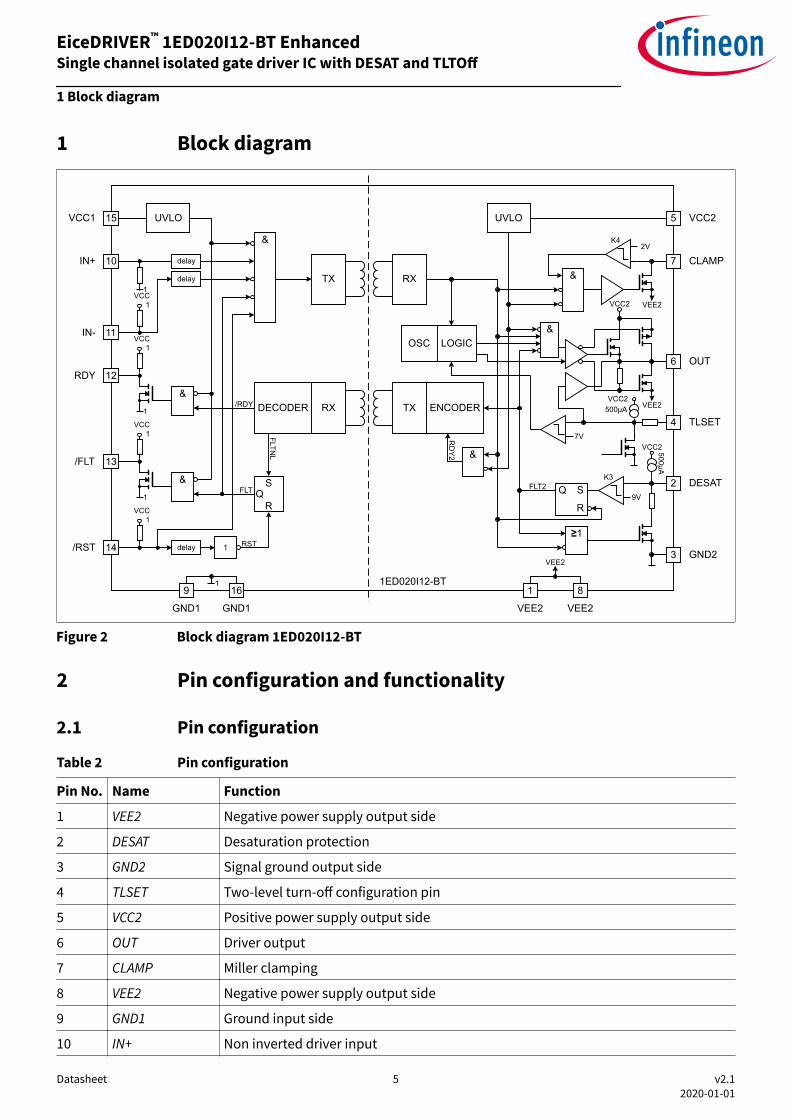
1 Block diagram
GND1
IN+
IN-
RDY
/RST
/FLT
VCC1
10
11
12
13
14
15
9
7
6
5
4
3
2
VCC2
OUT
GND2
CLAMP
DESAT
TLSET
delay
TX
RXDECODER
UVLO
TX
VEE2
2V
ENCODER
500µA
9V
K3
&
delay1
FLT
VCC1
VCC1
VCC1
VCC1
&
&
&
delay 1
QS
R
/RDY1
1
1
FLTNL
RST
UVLO
RX
&
VEE2
≥1
&VCC2
RD
Y2
FLT2
16 1 8
VEE2
GND1 VEE2
K4
VCC2
1ED020I12-BT
OSC
VCC2
7V
500µA
LOGIC
S
R
Q
VEE2
Figure 2 Block diagram 1ED020I12-BT
2 Pin configuration and functionality
2.1 Pin configuration
Table 2 Pin configuration
Pin No. Name Function
1 VEE2 Negative power supply output side
2 DESAT Desaturation protection
3 GND2 Signal ground output side
4 TLSET Two-level turn-off configuration pin
5 VCC2 Positive power supply output side
6 OUT Driver output
7 CLAMP Miller clamping
8 VEE2 Negative power supply output side
9 GND1 Ground input side
10 IN+ Non inverted driver input
EiceDRIVER™ 1ED020I12-BT EnhancedSingle channel isolated gate driver IC with DESAT and TLTOff
1 Block diagram
Datasheet 5 v2.12020-01-01

Table 2 Pin configuration (continued)
Pin No. Name Function
11 IN- Inverted driver input
12 RDY Ready output
13 /FLT Fault output, low active
14 /RST Reset input, low active
15 VCC1 Positive power supply input side
16 GND1 Ground input side
VEE2
IN+
IN-
RDY
/RST
/FLT
VCC1
GND1
VCC2
OUT
GND2
CLAMP
DESAT
TLSET
1
2
3
4
5
9
16
15
14
13
12
11
GND1
107
8
6
VEE2
Figure 3 1ED020I12-BT (top view)
2.2 Pin functionality
GND1
Ground connection of the input side.
IN+ non-inverting gate driver input
IN+ control signal for the driver output if IN- is set to low. (The IGBT is on if IN+ = high and IN- = low)A minimum pulse width is defined to make the IC robust against glitches at IN+. An internal pull-down resistorensures IGBT off-state.
IN- inverting gate driver input
IN- control signal for driver output if IN+ is set to high. (IGBT is on if IN- = low and IN+ = high)A minimum pulse width is defined to make the IC robust against glitches at IN-. An internal pull-up resistorensures IGBT off-state.
/RST reset input
Function 1: Enable/shutdown of the input chip. (The IGBT is off if /RST = low). A minimum pulse width is definedto make the IC robust against glitches at /RST.Function 2: Resets the DESAT fault-state of the chip if /RST is low for a time tRST. An internal pull-up resistor isused to ensure /FLT status output.
/FLT fault output
Open-drain output to report a desaturation error of the IGBT (/FLT is low if desaturation occurs)
EiceDRIVER™ 1ED020I12-BT EnhancedSingle channel isolated gate driver IC with DESAT and TLTOff
2 Pin configuration and functionality
Datasheet 6 v2.12020-01-01

RDY ready status
Open-drain output to report the correct operation of the device (RDY = high if both chips are above the UVLOlevel and the internal chip transmission is faultless).
VCC1
5 V power supply of the input chip
VEE2
Negative power supply pins of the output chip. If no negative supply voltage is available, all VEE2 pins have tobe connected to GND2.
DESAT desaturation detection input
Monitoring of the IGBT saturation voltage (VCE) to detect desaturation caused by short circuits. If OUT is high, VCEis above a defined value and a certain blanking time has expired, the desaturation protection is activated andthe IGBT is switched off. The blanking time is adjustable by an external capacitor.
CLAMP Miller clamping
Ties the gate voltage to ground after the IGBT has been switched off at a defined voltage to avoid a parasiticswitch-on of the IGBT.During turn-off, the gate voltage is monitored and the clamp output is activated when thegate voltage goes below 2 V (related to VEE2). The clamp is designed for a Miller current up to 2 A.
GND2 reference ground
Reference ground of the output chip.
OUT driver output
Output pin to drive an IGBT. The voltage is switched between VEE2 and VCC2. In normal operating mode VOUT iscontrolled by IN+, IN- and /RST. During error mode (UVLO, internal error or DESAT) VOUT is set to VEE2independent of the input control signals.
VCC2
Positive power supply pin of the output side.
TLSET two-level turn-off configuration
Circuitry at TLSET adjust the two-level turn-off time with an external capacitor to GND2 and the two levelvoltage with an external Zener diode to GND2.
3 Functional descriptionThe 1ED020I12-BT is an advanced IGBT gate driver that can be also used for driving power MOS devices. Controland protection functions are included to enable the design of high reliability systems.The device consists of two galvanic separated parts. The input chip can be directly connected to a standard 5 VDSP or microcontroller with CMOS in/output and the output chip is connected to the high voltage side.The rail-to-rail driver output enables the user to provide easy clamping of the IGBTs gate voltage during shortcircuit of the IGBT. So an increase of short circuit current due to the feedback via the Miller capacitance can beavoided. Further, a rail-to-rail output reduces power dissipation on a system-level.The device also includes IGBT desaturation protection with /FLT status output.A two-level turn-off feature with adjustable delay protects against excessive overvoltage at turn-off in case ofovercurrent or short circuit condition. The same delay is applied at turn-on to prevent pulse width distortion.
EiceDRIVER™ 1ED020I12-BT EnhancedSingle channel isolated gate driver IC with DESAT and TLTOff
3 Functional description
Datasheet 7 v2.12020-01-01

The RDY status output reports if the device is supplied and operates correctly.
GND1
IN+
IN-
RDY
/FLT
/RST
VCC1
OUT
VCC2
GND2
CLAMP
DESAT
+5V
VEE2
SGND
IN+
RDY
FLT
RST
+15V
-8V
TLSET
10R
1k10k
10k
10R
220p47p10V
1µ
1µ
100n
Figure 4 Application example bipolar supply
3.1 SupplyThe driver 1ED020I12-BT is designed to support two different supply configurations, bipolar supply andunipolar supply.In bipolar supply the driver is typically supplied with a positive voltage of 15 V at VCC2 and a negative voltage of -8 V at VEE2. Negative supply prevents a dynamic turn on due to the additional charge which is generated fromIGBT input capacitance times negative supply voltage. If an appropriate negative supply voltage is used,connecting CLAMP to IGBT gate is redundant and therefore typically not necessary.For unipolar supply configuration the driver is typically supplied with a positive voltage of 15 V at VCC2.Erratically dynamic turn on of the IGBT could be prevented with active Miller clamp function, so CLAMP outputis directly connected to IGBT gate.
GND1
IN+
IN-
RDY
/FLT
/RST
VCC1
OUT
VCC2
GND2
CLAMP
DESAT
+5V
VEE2
SGND
IN+
RDY
FLT
RST
+15V
TLSET
10R
1k10k
10k
10R
220p47p10V
1µ100n
Figure 5 Application example unipolar supply
3.2 Internal protection features
3.2.1 Undervoltage lockout (UVLO)To ensure correct switching of IGBTs the device is equipped with an undervoltage lockout for both chips, refer to Figure 16.If the power supply voltage VVCC1 of the input chip drops below VUVLOL1 a turn-off signal is sent to the outputchip before power-down. The IGBT is switched off and the signals at IN+ and IN- are ignored as long as VVCC1reaches the power-up voltage VUVLOH1.If the power supply voltage VVCC2 of the output chip goes down below VUVLOL2 the IGBT is switched off andsignals from the input chip are ignored as long as VVCC2 reaches the power-up voltage VUVLOH2. VEE2 is notmonitored, otherwise negative supply voltage range from 0 V to -12 V would not be possible.
EiceDRIVER™ 1ED020I12-BT EnhancedSingle channel isolated gate driver IC with DESAT and TLTOff
3 Functional description
Datasheet 8 v2.12020-01-01

OUT
IN+
VCC2
VUVLOH2
IDESAT
tPDON tPDOFF
RDY
Figure 6 VCC2 ramp up
VZ
OUT
TLSET
IN+
VCC2 VUVLOH2
RDY
/FLT
VUVLOL2
tTLSET
tPDON
tPDD tPDD tPDD
Figure 7 VCC2 ramp down and VCC2 drop
3.2.2 RDY ready status outputThe RDY output shows the status of three internal protection features.• UVLO of the input chip• UVLO of the output chip after a short delay• Internal signal transmission after a short delayIt is not necessary to reset the RDY signal since its state only depends on the status of the former mentionedprotection signals.
EiceDRIVER™ 1ED020I12-BT EnhancedSingle channel isolated gate driver IC with DESAT and TLTOff
3 Functional description
Datasheet 9 v2.12020-01-01

3.2.3 Watchdog timerDuring normal operation the internal signal transmission is monitored by a watchdog timer. If the transmissionfails for a given time, the IGBT is switched off and the RDY ready output reports an internal error.
3.2.4 Active shut-downThe active shut-down feature ensures a safe IGBT off-state if the output chip is not connected to the powersupply, IGBT gate is clamped at OUT to VEE2.
3.3 Non-inverting and inverting inputsThere are two possible input modes to control the IGBT. At non-inverting mode IN+ controls the driver outputwhile IN- is set to low. At inverting mode IN- controls the driver output while IN+ is set to high, please see Figure14. A minimum input pulse width is defined to filter occasional glitches.
3.4 Driver outputThe output driver sections uses only MOSFETs to provide a rail-to-rail output. This feature permits that tightcontrol of gate voltage during on-state and short circuit can be maintained as long as the drivers supply isstable.Due to the low internal voltage drop, switching behavior of the IGBT is predominantly governed by the gateresistor. Furthermore, it reduces the power to be dissipated by the driver.
3.5 Two-level turn-offThe two-level turn-off introduces a second turn off voltage level at the driver output in between ON- and OFFlevel. This additional level ensures lower VCE overshoots at turn off by reducing gate emitter voltage of the IGBTat short circuits or over current events. The VGE level is adjusting the current of the IGBT at the end two-levelturn-off interval, the required timing is depending on stray inductance and over current at beginning of two-level turn-off interval.
OUT
TLSET
IN+
tPDONADJ
tADJ1
VZDIODE
VZDIODE
tTLSET
tPD
tTLFALL
tPD
tTLSET
VTLSET , typ. 7V
Figure 8 Typical two-level turn-off switching behavior
Reference voltage level and hold up time could be adjusted at TLSET pin. The reference voltage is set by therequired Zener diode connected between pin TLSET and GND2. The holdup time is set by the capacitorconnected to the same pin TLSET and GND2.
EiceDRIVER™ 1ED020I12-BT EnhancedSingle channel isolated gate driver IC with DESAT and TLTOff
3 Functional description
Datasheet 10 v2.12020-01-01

5
4
3
2
1
t TLS
ET [µ
s]
50 100 150 200CTLSET [pF]
00
Figure 9 Typical tTLSET time over CTLSET capacitance
The hold time can be adjusted during switch on using the whole capacitance connected at pin TLSET includingcapacitor, parasitic wiring capacitance and junction capacitance of Zener diode. When a switch on signal isgiven the IC starts to discharge CTLSET. Discharging CTLSET is stopped after 500 ns. Then CTLSET is charged with aninternal charge current ITLSET. When the voltage of the capacitor CTLSET exceeds 7 V a second current sourcestarts charging CTLSET up to VZDIODE. At the end of this discharge-charge cycle the gate driver is switched on.The time between IN initiated switch-on signal (minus an internal propagation delay of approximately 200 ns)and switch-on of the gate drive is sampled and stored digitally. It represents the two-level turn-off set timetTLSET during switch-off. Due to digitalization the tPDon time can vary in time steps of 50 ns.If switch off is initiated from IN+, IN- or /RST signal, the gate driver is switched off immediately after internalpropagation delay of approximately 200 ns and VOUT begins to decrease to the second gate voltage level.For switch off initiated by DESAT, the gate driver switch off is delayed by desaturation sense to OUT delay,afterwards VOUT begins to decrease to the second gate voltage level.For reaching second gate voltage level the output voltage VOUT is sensed and compared with the Zener voltageVZDIODE. When VOUT falls below the reference voltage VZDIODE of the Zener diode the switch off process isinterrupted and VOUT is adjusted to VZDIODE. OUT is switched to VEE2 after the holdup time has passed.The two-level turn-off function cannot be disabled.
3.6 Minimal on-/off-time at two-level turn-off operationThe 1ED020I12-BT driver requires minimal on and off time for proper operation in the application.
OUT
TLSET
IN+
tPDON
tPDOFF
tPDON
tPD
tTLSETtTLSET
tTLSET
tPD
Figure 10 Short switch-on pulses
Minimal on time must be greater than the adjustable two level plateau time tTLSET, shorter on times will besuppressed by generating of the plateau time. Due to the short on time, the voltage at TLSET pin does not reachthe comparator threshold; therefore the driver does not turn on.
EiceDRIVER™ 1ED020I12-BT EnhancedSingle channel isolated gate driver IC with DESAT and TLTOff
3 Functional description
Datasheet 11 v2.12020-01-01
OUT
TLSET
IN+
tPDOFF tPDOFFtPDON
tPDtPDtPDON
tPDOFF
tTLSET tTLSET tTLSET
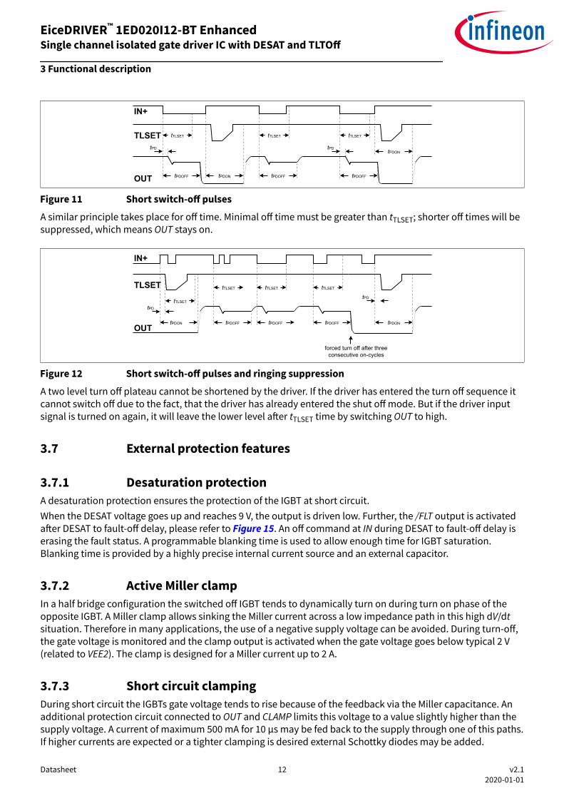
Figure 11 Short switch-off pulses
A similar principle takes place for off time. Minimal off time must be greater than tTLSET; shorter off times will besuppressed, which means OUT stays on.
OUT
TLSET
IN+
tPDON tPDOFF
tPD
tPDOFF tPDOFF tPDON
tPD
forced turn off after three consecutive on-cycles
tTLSET tTLSET tTLSET
tTLSET
Figure 12 Short switch-off pulses and ringing suppression
A two level turn off plateau cannot be shortened by the driver. If the driver has entered the turn off sequence itcannot switch off due to the fact, that the driver has already entered the shut off mode. But if the driver inputsignal is turned on again, it will leave the lower level after tTLSET time by switching OUT to high.
3.7 External protection features
3.7.1 Desaturation protectionA desaturation protection ensures the protection of the IGBT at short circuit.When the DESAT voltage goes up and reaches 9 V, the output is driven low. Further, the /FLT output is activatedafter DESAT to fault-off delay, please refer to Figure 15. An off command at IN during DESAT to fault-off delay iserasing the fault status. A programmable blanking time is used to allow enough time for IGBT saturation.Blanking time is provided by a highly precise internal current source and an external capacitor.
3.7.2 Active Miller clampIn a half bridge configuration the switched off IGBT tends to dynamically turn on during turn on phase of theopposite IGBT. A Miller clamp allows sinking the Miller current across a low impedance path in this high dV/dtsituation. Therefore in many applications, the use of a negative supply voltage can be avoided. During turn-off,the gate voltage is monitored and the clamp output is activated when the gate voltage goes below typical 2 V(related to VEE2). The clamp is designed for a Miller current up to 2 A.
3.7.3 Short circuit clampingDuring short circuit the IGBTs gate voltage tends to rise because of the feedback via the Miller capacitance. Anadditional protection circuit connected to OUT and CLAMP limits this voltage to a value slightly higher than thesupply voltage. A current of maximum 500 mA for 10 μs may be fed back to the supply through one of this paths.If higher currents are expected or a tighter clamping is desired external Schottky diodes may be added.
EiceDRIVER™ 1ED020I12-BT EnhancedSingle channel isolated gate driver IC with DESAT and TLTOff
3 Functional description
Datasheet 12 v2.12020-01-01

3.8 /RST resetThe reset input has two functions.• /RST is in charge of setting back the /FLT output. If /RST is low longer than a given time, /FLT will be cleared
at the rising edge of /RST, refer to Figure 15; otherwise, it will remain unchanged• /RST works as enable/shutdown of the input logic, refer to Figure 14
4 Electrical parameters
4.1 Absolute maximum ratingsNote: Absolute maximum ratings are defined as ratings, which when being exceeded may lead to
destruction of the integrated circuit. Unless otherwise noted all parameters refer to GND1.
Table 3 Absolute maximum ratings
Parameter Symbol Values Unit Note /Test conditionMin. Max.
Positive power supply output side VVCC2 -0.3 20 V 1)
Negative power supply output side VVEE2 -12 0.3 V 1)
Maximum power supply voltage output side(VVCC2 - VVEE2)
Vmax2 – 28 V –
Gate driver output VOUT VVEE2-0.3 VVCC2+0.3 V –
Gate driver high output maximum current IOUT – 2.4 A t = 2 µs
Gate & clamp driver low output maximumcurrent
IOUT – 2.4 A t = 2 µs
Maximum short circuit clamping time tCLP – 10 μs ICLAMP/OUT =500 mA
Positive power supply input side VVCC1 -0.3 6.5 V –
Logic input voltages (IN+,IN-,/RST) VLogicIN -0.3 6.5 V –
Opendrain Logic output voltage (/FLT) V/FLT -0.3 6.5 V –
Opendrain Logic output voltage (RDY) VRDY -0.3 6.5 V –
Opendrain Logic output current (/FLT) I/FLT – 10 mA –
Opendrain Logic output current (RDY) IRDY – 10 mA –
Pin DESAT voltage VDESAT -0.3 VVCC2 +0.3 V 1)
Pin CLAMP voltage VCLAMP -0.3 VVCC2+0.32)
V 3)
Input to output isolation voltage (GND2) Voffset -1200 1200 V
Junction temperature TJ -40 150 °C –
1 With respect to GND2.2 May be exceeded during short circuit clamping.3 With respect to VEE2.
EiceDRIVER™ 1ED020I12-BT EnhancedSingle channel isolated gate driver IC with DESAT and TLTOff
4 Electrical parameters
Datasheet 13 v2.12020-01-01

Table 3 Absolute maximum ratings (continued)
Parameter Symbol Values Unit Note /Test conditionMin. Max.
Storage temperature TS -55 150 °C –
Power dissipation, per input part PD, IN – 100 mW 4)@TA = 25°C
Power dissipation, at output side PD, OUT – 700 mW 4) @TA = 25°C
Thermal resistance (input side) RthJA,IN – 160 K/W 4) @TA = 25°C
Thermal resistance (output side) RthJA,OUT – 125 K/W 4) @TA = 25°C
ESD capability VESD,HBM – 1.5 kV Human BodyModel5)
4.2 Operating parametersNote: Within the operating range the IC operates as described in the functional description. Unless
otherwise noted all parameters refer to GND1.
Table 4 Operating parameters
Parameter Symbol Values Unit Note /Test conditionMin. Max.
Positive power supply output side VVCC2 13 20 V 6)
Negative power supply output side VVEE2 -12 0 V 6)
Maximum power supply voltageoutput side (VVCC2 - VVEE2)
Vmax2 – 28 V –
Positive power supply input side VVCC1 4.5 5.5 V –
Logic input voltages (IN+,IN-,/RST) VLogicIN -0.3 5.5 V –
Pin CLAMP voltage VCLAMP VVEE2-0.3 VVCC27) V –
Pin DESAT voltage VDESAT -0.3 VVCC2 V 6)
Pin TLSET voltage VTLSET -0.3 VVCC2 V 6)
Ambient temperature TA -40 105 °C –
Common mode transient immunity8) |dVISO/dt| – 50 kV/μs @ 500 V
4.3 Recommended operating parameters
4 Output IC power dissipation is derated linearly at 10 mW/°C above 62°C. Input IC power dissipation doesnot require derating. See Figure 18 for reference layouts for these thermal data. Thermal performancemay change significantly with layout and heat dissipation of components in close proximity.
5 According to EIA/JESD22-A114-B (discharging a 100 pF capacitor through a 1.5 kΩ series resistor).6 With respect to GND2.7 May be exceeded during short circuit clamping.8 The parameter is not subject to production test - verified by design/characterization
EiceDRIVER™ 1ED020I12-BT EnhancedSingle channel isolated gate driver IC with DESAT and TLTOff
4 Electrical parameters
Datasheet 14 v2.12020-01-01

Note: Unless otherwise noted all parameters refer to GND1.
Table 5 Recommended operating parameters
Parameter Symbol Value Unit Note / Test condition
Positive power supply output side VVCC2 15 V 9)
Negative power supply output side VVEE2 -8 V 9)
Positive power supply input side VVCC1 5 V –
9 With respect to GND2.
EiceDRIVER™ 1ED020I12-BT EnhancedSingle channel isolated gate driver IC with DESAT and TLTOff
4 Electrical parameters
Datasheet 15 v2.12020-01-01

4.4 Electrical characteristicsNote: The electrical characteristics include the spread of values in supply voltages, load and junction
temperatures given below. Typical values represent the median values at TA = 25°C. Unless otherwisenoted all voltages are given with respect to their respective GND (GND1 for pins 9 to 16, GND2 for pins1 to 8).
4.4.1 Voltage supply
Table 6 Voltage supply
Parameter Symbol Values Unit Note / TestconditionMin. Typ. Max.
UVLO threshold inputchip
VUVLOH1 – 4.1 4.3 V –
VUVLOL1 3.5 3.8 – V –
UVLO hysteresis inputchip (VUVLOH1 - VUVLOL1)
VHYS1 0.15 – – V –
UVLO threshold outputchip
VUVLOH2 – 12.0 12.6 V –
VUVLOL2 10.4 11.0 – V –
UVLO hysteresis outputchip (VUVLOH2 - VUVLOL2)
VHYS2 0.7 0.9 – V –
Quiescent current inputchip
IQ1 – 7 9 mA VVCC1 = 5 VIN+ = High,IN- = Low=>OUT = High,RDY = High,/FLT = High
Quiescent currentoutput chip
IQ2 – 4 6 mA VVCC2 = 15 VVVEE2 = -8 VIN+ = High,IN- = Low=>OUT = High,RDY = High,/FLT = High
EiceDRIVER™ 1ED020I12-BT EnhancedSingle channel isolated gate driver IC with DESAT and TLTOff
4 Electrical parameters
Datasheet 16 v2.12020-01-01

4.4.2 Logic input and output
Table 7 Logic input and output
Parameter Symbol Values Unit Note / TestconditionMin. Typ. Max.
IN+,IN-, /RST low input voltage VIN+,L, VIN-,L,V/RST,L
– – 1.5 V –
IN+,IN-, /RST high input voltage VIN+,H, VIN-,H,V/RST,H
3.5 – – V –
IN-, /RST input current IIN-, I/RST -400 -100 – μA VIN- = GND1V/RST = GND1
IN+ input current IIN+, – 100 400 μA VIN+ = VCC1
RDY,/FLT pull-up current IP,RDY, IP,/FLT -400 -100 – μA VRDY = GND1V/FLT = GND1
Input pulse suppression IN+, IN- tMININ+,tMININ-
30 40 – ns –
Input pulse suppression /RSTfor enable/shutdown
tMINRST 30 40 – ns –
Pulse width /RST forreseting /FLT
t/RST 800 – – ns –
/FLT low woltage V/FLT,L – – 300 mV ISINK,/FLT = 5 mA
RDY low voltage VRDY,L – – 300 mV ISINK,RDY = 5 mA
EiceDRIVER™ 1ED020I12-BT EnhancedSingle channel isolated gate driver IC with DESAT and TLTOff
4 Electrical parameters
Datasheet 17 v2.12020-01-01

4.4.3 Gate driver
Table 8 Gate driver
Parameter Symbol Values Unit Note / TestconditionMin. Typ. Max.
High level outputvoltage
VOUTH1 VCC2 -1.2 VCC2 -0.8 – V IOUTH = -20 mA
VOUTH2 VCC2 -2.5 VCC2-2.0 – V IOUTH = -200 mA
VOUTH3 VCC2 -9 VCC2-5 – V IOUTH = -1 A
VOUTH4 VCC2-10 – V IOUTH = -2 A
High level output peakcurrent
IOUTH -1.5 -2.0 – A IN+ = High,IN- = Low;OUT = High
Low level outputvoltage
VOUTL1 – VVEE2 +0.04 VVEE2+0.09 V IOUTL = 20 mA
VOUTL2 – VVEE2 +0.3 VVEE2+0.85 V IOUTL = 200 mA
VOUTL3 – VVEE2 +2.1 VVEE2+5 V IOUTL = 1 A
VOUTL4 – VVEE2 +7 – V IOUTL = 2 A
Low level output peakcurrent
IOUTL 1.5 2.0 – A IN+ = Low,IN- = Low;OUT = Low,VVCC2 = 15 V,VVEE2 = -8 V
4.4.4 Active Miller clamp
Table 9 Active Miller clamp
Parameter Symbol Values Unit Note / Test condition
Min. Typ. Max.
Low level clampvoltage
VCLAMPL1 – VVEE2+0.03 VVEE2 +0.08 V IOUTL = 20 mA
VCLAMPL2 – VVEE2+0.3 VVEE2 +0.8 V IOUTL = 200 mA
VCLAMPL3 – VVEE2+1.9 VVEE2 +4.8 V IOUTL = 1 A
Low level clampcurrent
ICLAMPL 2 – – A 10)
Clamp thresholdvoltage
VCLAMP 1.6 2.1 2.4 V Related to VEE2
10 The parameter is not subject to production test - verified by design/characterization
EiceDRIVER™ 1ED020I12-BT EnhancedSingle channel isolated gate driver IC with DESAT and TLTOff
4 Electrical parameters
Datasheet 18 v2.12020-01-01

4.4.5 Short circuit clamping
Table 10 Short circuit clamping
Parameter Symbol Values Unit Note / TestconditionMin. Typ. Max.
Clamping voltage (OUT)(VOUT - VVCC2)
VCLPout – 0.8 1.3 V IN+ = High,IN- = Low,OUT = HighIOUT = 500 mA pulsetest,tCLPmax = 10 μs)
Clamping voltage(CLAMP) (VVCLAMP-VVCC2)
VCLPclamp – 1.3 – V IN+ = High,IN- = Low,OUT = HighICLAMP = 500 mA(pulse test,tCLPmax = 10 μs)
Clamping voltage(CLAMP)
VCLPclamp – 0.7 1.1 V IN+ = High,IN- = Low,OUT = HighICLAMP = 20 mA
4.4.6 Dynamic characteristicsDynamic characteristics are measured with VVCC1 = 5 V, VVCC2 = 15 V and VVEE2 = -8 V.
Table 11 Dynamic characteristics
Parameter Symbol Values Unit Note / TestconditionMin. Typ. Max.
Input IN+, IN- to outputpropagation delay ONand OFF
tPDON,tPDO
FF
1.5 1.75 2.0 µs CTLSET = 0TA= 25°C
Input IN+, IN- to outputpropagation delaydistortion (tPDOFF - tPDON)
tPDISTO -40 -10 20 ns
IN+, IN- input to outputpropagation delay ONvariation due to temp
tPDON,t – – 200 ns 11)CTLSET = 0
IN+, IN- input to outputpropagation delay OFFvariation due to temp
tPDOFF,t – – 230 ns 11)CTLSET = 0
11 The parameter is not subject to production test - verified by design/characterization
EiceDRIVER™ 1ED020I12-BT EnhancedSingle channel isolated gate driver IC with DESAT and TLTOff
4 Electrical parameters
Datasheet 19 v2.12020-01-01

Table 11 Dynamic characteristics (continued)
Parameter Symbol Values Unit Note / TestconditionMin. Typ. Max.
IN+, IN- input to outputpropagation delaydistortion variation dueto temp (tPDOFF-tPDON)
tPDISTO,t – – 25 ns 11)CTLSET = 0
Rise time tRISE 10 30 60 ns CLOAD = 1 nFVL 10%,VH 90%
150 400 800 ns CLOAD = 34 nFVL 10%,VH 90%
Fall time tFALL 10 20 40 ns CLOAD = 1 nFVL 10%,VH 90%
100 250 500 ns CLOAD = 34 nFVL 10%,VH 90%
4.4.7 Desaturation protection
Table 12 Desaturation protection
Parameter Symbol Values Unit Note / TestconditionMin. Typ. Max.
Blanking capacitorcharge current
IDESATC 450 500 550 μA VVCC2 =15 V,VVEE2=- 8 VVDESAT = 2 V
Blanking capacitordischarge current
IDESATD 11 15 – mA VVCC2 =15 V,VVEE2 = -8 VVDESAT = 6 V
Desaturation referencelevel
VDESAT 8.5 9 9.5 V VVCC2 = 15 V
Desaturation sense toOUT low delay
tDESATOUT – 250 320 ns VOUT = 90%CLOAD = 1 nF
Desaturation senseto /FLT low delay
tDESATFLT – – 2.25 μs V/FLT = 10%;I/FLT = 5 mA
11 The parameter is not subject to production test - verified by design/characterization
EiceDRIVER™ 1ED020I12-BT EnhancedSingle channel isolated gate driver IC with DESAT and TLTOff
4 Electrical parameters
Datasheet 20 v2.12020-01-01

Table 12 Desaturation protection (continued)
Parameter Symbol Values Unit Note / TestconditionMin. Typ. Max.
Desaturation lowvoltage
VDESATL 40 70 110 mV IN+ = low, IN- = low,OUT = low
EiceDRIVER™ 1ED020I12-BT EnhancedSingle channel isolated gate driver IC with DESAT and TLTOff
4 Electrical parameters
Datasheet 21 v2.12020-01-01

4.4.8 Active shut-down
Table 13 Active shut-down
Parameter Symbol Values Unit Note / TestconditionMin. Typ. Max.
Active shut-down voltage VACTSD12) – – 2.0 V IOUT = -200 mA,
VVCC2 open
4.4.9 Two-level turn-off
Table 14 Two-level turn-off
Parameter Symbol Values Unit Note / TestconditionMin. Typ. Max.
External reference voltagerange (Zener-Diode)
VZDIODE 7.5 – VCC2-0.5 V –
Reference voltage forsetting two-level delaytime
VTLSET 6.6 7 7.3 V –
Current for setting two-level delay time andexternal reference voltage(Zener-Diode)
ITLSET 420 500 550 µA VTLSET = 10 V
Exteral capacitance range CTLSET 0 – 220 pF –
12 With reference to VEE2
EiceDRIVER™ 1ED020I12-BT EnhancedSingle channel isolated gate driver IC with DESAT and TLTOff
4 Electrical parameters
Datasheet 22 v2.12020-01-01

5 Insulation characteristicsInsulation characteristics are guaranteed only within the safety maximum ratings which must be ensured byprotective circuits in application. Surface mount classification is class A in accordance with CECCOO802.This coupler is suitable for rated insulation only within the safety ratings. Compliance with the safety ratingsshall be ensured by means of suitable protective circuits.
5.1 Tested according to VDE 0884-10 (Standard expired on Dec. 31, 2019)Since the standard has expired on December 31, 2019, the product and its testing has not been changed.
Table 15 According to VDE 0884-10 (Standard expired on Dec. 31, 2019)
Description Symbol Characteristic Unit
Installation classification per EN 60664-1, Table 1for rated mains voltage ≤ 150 V (rms)for rated mains voltage ≤ 300 V (rms)for rated mains voltage ≤ 600 V (rms)
I-IVI-IIII-II
–
Climatic classification (IEC68-1) 40/105/21 –
Pollution degree (EN 60664-1) 2 –
Minimum external clearance CLR 8.12 mm
Minimum external creepage CPG 8.24 mm
Minimum comparative tracking index CTI 175 –
Maximum repetitive insulation voltage VIORM 1420 V (pk)
Input to output test voltage, method b13)
VIORM * 1.875 = VPR, 100% production test with tm = 1 sec,partial discharge < 5 pC
VPR 2663 V (pk)
Input to output test voltage, method a13)
VIORM * 1.6 = VPR, 100% production test with tm = 60 sec,partial discharge < 5 pC
VPR 2272 V (pk)
Highest allowable overvoltage VIOTM 6000 V (pk)
Maximum surge insulation voltage VIOSM 6000 V
Insulation resistance at TS, VIO = 500 V RIO > 109 Ω
5.2 Recognized under UL 1577 (File E311313)
Table 16 Recognized under UL 1577
Description Symbol Characteristic Unit
Insulation withstand voltage / 1 min VISO 3750 V (rms)
Insulation test voltage / 1 s VISO,test 4500 V (rms)
13 Refer to VDE 0884 for a detailed description of Method a and Method b partial discharge test profiles.
EiceDRIVER™ 1ED020I12-BT EnhancedSingle channel isolated gate driver IC with DESAT and TLTOff
5 Insulation characteristics
Datasheet 23 v2.12020-01-01

6 Timing diagrams
IN+
OUTtPDON
50%
50%
tPDOFF
10%
90%
tRISE tFALL
Figure 13 Propagation delay, rise and fall time
OUT
/RST
IN+
IN-
Figure 14 Typical switching behavior
VDESAT typ. 9V
>tRSTmin
OUT
DESAT
IN+
/FLT
/RST
tPDON
tDESATFLT tDESATFLT
tDESATOUT
tTLSET
tDESATOUT
tTLSET
Figure 15 DESAT switch-off behavior
EiceDRIVER™ 1ED020I12-BT EnhancedSingle channel isolated gate driver IC with DESAT and TLTOff
6 Timing diagrams
Datasheet 24 v2.12020-01-01

OUT
/RST
IN+
VCC2
VCC1
RDY
/FLT
ESD diode conduction
VUVLOH2VUVLOL2
VUVLOH1VUVLOL1
Figure 16 UVLO behavior
EiceDRIVER™ 1ED020I12-BT EnhancedSingle channel isolated gate driver IC with DESAT and TLTOff
6 Timing diagrams
Datasheet 25 v2.12020-01-01

7 Package outline
Figure 17 PG-DSO-16-15 300 mil body
8 Application notes
8.1 Reference layout for thermal dataThe PCB layout shown in Figure 18 represents the reference layout used for the thermal characterization. Pins 9and 16 (GND1) and pins 1 and 8 (VEE2) require ground plane connections for achieving maximum powerdissipation. The 1ED020I12-BT is conceived to dissipate most of the heat generated through this pins.
EiceDRIVER™ 1ED020I12-BT EnhancedSingle channel isolated gate driver IC with DESAT and TLTOff
7 Package outline
Datasheet 26 v2.12020-01-01

Figure 18 Reference layout for thermal data (Copper thickness 102 μm)
8.2 Printed circuit board guidelinesFollowing factors should be taken into account for an optimum PCB layout.• Sufficient spacing should be kept between high voltage isolated side and low voltage side circuits.• The same minimum distance between two adjacent high-side isolated parts of the PCB should be
maintained to increase the effective isolation and reduce parasitic coupling.• In order to ensure low supply ripple and clean switching signals, bypass capacitor trace lengths should be
kept as short as possible.• Lowest trace length for VEE2 to GND2 decoupling could be achieved with capacitor closed to pins 1 and 3.
Revision historyDocumentversion
Date ofrelease
Description of changes
v2.1 2020-01-01 • Update to new template• Editorial changes to headlines, descriptions and figures• Update to VDE 0884-10 expiration date, product and testing have not been
changed
v2.0 2012-07-31 • first data sheet release
EiceDRIVER™ 1ED020I12-BT EnhancedSingle channel isolated gate driver IC with DESAT and TLTOff
Revision history
Datasheet 27 v2.12020-01-01

TrademarksAll referenced product or service names and trademarks are the property of their respective owners.
Edition 2020-01-01Published byInfineon Technologies AG81726 Munich, Germany © 2020 Infineon Technologies AGAll Rights Reserved. Do you have a question about anyaspect of this document?Email: [email protected] Document referenceIFX-sjq1576063276734
IMPORTANT NOTICEThe information given in this document shall in noevent be regarded as a guarantee of conditions orcharacteristics (“Beschaffenheitsgarantie”) .With respect to any examples, hints or any typical valuesstated herein and/or any information regarding theapplication of the product, Infineon Technologieshereby disclaims any and all warranties and liabilities ofany kind, including without limitation warranties ofnon-infringement of intellectual property rights of anythird party.In addition, any information given in this document issubject to customer’s compliance with its obligationsstated in this document and any applicable legalrequirements, norms and standards concerningcustomer’s products and any use of the product ofInfineon Technologies in customer’s applications.The data contained in this document is exclusivelyintended for technically trained staff. It is theresponsibility of customer’s technical departments toevaluate the suitability of the product for the intendedapplication and the completeness of the productinformation given in this document with respect to suchapplication.
WARNINGSDue to technical requirements products may containdangerous substances. For information on the typesin question please contact your nearest InfineonTechnologies office.Except as otherwise explicitly approved by InfineonTechnologies in a written document signed byauthorized representatives of Infineon Technologies,Infineon Technologies’ products may not be used inany applications where a failure of the product orany consequences of the use thereof can reasonablybe expected to result in personal injury