efficient optical absorption in thin-film solar cells
TRANSCRIPT

Efficient optical absorption in thin-film solar cells
Lili Yang,1 Yimin Xuan,1,2,* and Junjie Tan1 1School of Energy and Power Engineering, Nanjing University of Science & Technology, Nanjing 210094, China
2 Nanjing University of Aeronautics & Astronauics, Nanjing 210016, China *[email protected]
Abstract: In order to improve the optical absorption of hydrogenated amorphous silicon (a-Si:H) thin film solar cells, a new structure consisted of ITO layer with the nonresonant nanoparticles embedded in it and a-Si:H layer, is proposed. By optimizing both the thickness of a-Si:H layer and nanoparticles size, the effects of Fabry-Perot resonance and the scattering of incident light are discussed and analyzed. It is demonstrated that the enhanced optical absorption can be achieved due to the coupling of incident light and nanostructure, simultaneously the proposed structure can be considered as gradient refractive index structure to restrain the reflection at the interface of ITO and a-Si:H thin film. ©2011 Optical Society of America OCIS codes: (050.2230) Fabry-Perot resonance; (290.5850) Scattering; (310.6860) Thin film; (350.4990) Particles.
References and links 1. A. Krasnov, “Light scattering by textured transparent electrodes for thin-film silicon solar cells,” Sol. Energy
Mater. Sol. Cells 94(10), 1648–1657 (2010). 2. W. Wang, S. Wu, K. Reinhardt, Y. Lu, and S. Chen, “Broadband light absorption enhancement in thin-film
silicon solar cells,” Nano Lett. 10(6), 2012–2018 (2010). 3. D. Madzharov, R. Dewan, and D. Knipp, “Influence of front and back grating on light trapping in
microcrystalline thin-film silicon solar cells,” Opt. Express 19(Suppl 2), A95–A107 (2011). 4. L. Hu and G. Chen, “Analysis of optical absorption in silicon nanowire arrays for photovoltaic applications,”
Nano Lett. 7(11), 3249–3252 (2007). 5. J. Li, H. Y. Yu, S. M. Wong, G. Zhang, X. Sun, P. G.-Q. Lo, and D.-L. Kwong, “Si nanopillar array optimization
on Si thin lms for solar energy harvesting,” Appl. Phys. Lett. 95(3), 033102 (2009). 6. Y. A. Akimov and W. S. Koh, “Resonant and nonresonant plasmonic nanoparticle enhancement for thin-film
silicon solar cells,” Nanotechnology 21(23), 235201 (2010). 7. E. Moulin, J. Sukmanowski, P. Luo, R. Carius, F. X. Royer, and H. Stiebig, “Improved light absorption in thin-film
silicon solar cells by integration of silver nanoparticles,” J. Non-Cryst. Solids 354(19–25) 2488–2491 (2008). 8. T. L. Temple, G. D. K. Mahanama, H. S. Reehal, and D. M. Bagnall, “Influence of localized surface plasmon
excitation in silver nanoparticles on the performance of silicon solar cells,” Sol. Energy Mater. Sol. Cells 93(11), 1978–1985 (2009).
9. Y. A. Akimov, W. S. Koh, S. Y. Sian, and S. Ren, “Nanoparticle-enhanced thin film solar cells: metallic or dielectric nanoparticles,” Appl. Phys. Lett. 96(7), 073111 (2010).
10. C. Hägglund, M. Zäch, G. Petersson, and B. Kasemo, “Electromagnetic coupling of light into a silicon solar cell by nanodisk plasmons,” Appl. Phys. Lett. 92(5), 053110 (2008).
11. Y. A. Akimov and W. S. Koh, “Design of plasmonic nanoparticles for efficient subwavelength light trapping in thin-film solar cells,” Plasmonics 6(1), 155–161 (2011).
12. K. R. Catchpole and A. Polman, “Plasmonic solar cells,” Opt. Express 16(26), 21793–21800 (2008). 13. D. B. Ge and Y. B. Yan, Finite-Difference Time-Domain Method for Electromagnetic Waves (Xidian University
Press, 2005). 14. A. Taflove and S. Hagness, Computational Electrodynamics: The Finite-Difference Time-Domain Method, 2nd
ed. (Artech House, 2000). 15. H. Piller, “Silicon (Amorphous) (a-Si),” and D. Y. Smith, E. Shiles and M. Inokuti, “The Optical Properties of
Metallic Aluminum,” in Handbook of Optical Constants of Solids, E.D. Palik, ed. (Academic 1985). 16. J. C. Maxwell-Garnett, “Colours in metal glasses and in metallic films,” Philos. Trans. R. Soc. Lond. 203(359-
371), 385–420 (1904). 17. C. F. Bohren and D. R. Huffman, “Absorption and Scattering of Light by Small Particles.” (Wiley 1998).
#150783 - $15.00 USD Received 8 Jul 2011; revised 20 Aug 2011; accepted 24 Aug 2011; published 2 Sep 2011(C) 2011 OSA 12 September 2011 / Vol. 19, No. S5 / OPTICS EXPRESS A1165

1. Introduction
Thin-film solar cells are promising and attractive for the low cost, nontoxicity and mature processing technology. However, the minority carrier diffusion length is so short that the conversion efficiency is relatively low. Hence, it is imperative to improve the effective optical absorption of the a-Si:H thin-film solar cells by optimizing the nanostructure and achieve a similar absorption of crystalline silicon solar cells. In the past years, variety of light-trapping schemes have been investigated, such as textured surfaces [1], gratings [2,3], nanostructures [4–6] and so on. Nevertheless, each of these approaches has its advantages and disadvantages. For the complicated surfaces, an increased surface recombination is produced owing to the large surfaces. For resonant metals, the excited surface plasmon polaritons lead to a parasitic absorption inside the nanoparticles [7,8]. Therefore, aluminum, whose surface plasmons frequency lies in the ultraviolet range, would be used in the next discussion instead of commonly used silver.
Since nonresonant plasmonic metal (Al) is involved in this work, the scattering from Al nanostructures should be in great concert. Enhanced absorption from scattering of metal nanoparticles has been investigated in different types of solar cells [9–12]. These results are very important and have great guiding significance to subsequent research. Based on the scattering effect, further optimizing of nanostructures is to get better broadband absorption.
In this paper, a new structure of a-Si:H thin film solar cell with a hybrid ITO layer in which some nonresonant nanoparticles are embedded is proposed. The whole structure is attached on the substrate of Al which plays both the roles of antireflection and electrode. The effects of the sizes and locations of the embedded nanoparticles are analyzed. This design not only optimizes the light absorption over the entire solar spectrum, but also avoids oxidation of metallic nanoparticles. It is quite important to evaluate the factors that affect the optical absorption.
2. Simulation Model
The schematic diagram of the proposed design is shown in Fig. 1. The bottom electrode is a thin layer of Al with a thickness of h1. The a-Si:H thin layer of a thickness h2 is attached onto the Al thin layer. Al nanoparticles with a feature period of Λ, radius of r, are deposited on the top of the a-Si:H thin layer. A thin layer of ITO with a thickness of h3 is deposited on the top surface to cover the Al nanoparticals and forms the top electrode.
Fig. 1. Schematic diagram and cross-section view of thin film solar cells structure used.
The optical reflection and absorption of the structure at the normal incidence on the surface of the a-Si:H thin film solar cells can be obtained from Maxwell equation by using FDTD method [13,14]:
#150783 - $15.00 USD Received 8 Jul 2011; revised 20 Aug 2011; accepted 24 Aug 2011; published 2 Sep 2011(C) 2011 OSA 12 September 2011 / Vol. 19, No. S5 / OPTICS EXPRESS A1166

,
t
t
ε
µ
∂∇× =
∂=
∂∇× = −
∂=
DH
D E
BE
B H
(1)
where E is the electric field, H is the magnetic field, ε is complex permittivity, and μ is complex permeability. For the ε being a function of the frequency, the frequency domain equation ( ) ( ) ( )ω ε ω ω=D E should be transformed to the time domain by using the auxiliary difference equation (ADE). For the whole computation, the structure proposed in this work is assumed to be opaque and then all the photons through the surface can be absorbed. The incident wave is along the z-direction. The modal absorbing boundary conditions (modal ABCs) are used in z-direction. Electric and magnetic fields on the termination boundary can be calculated according to the electromagnetic field at the nodes next to the boundary by means of the modal current and voltage. And the periodic boundary conditions (PBCs) are employed in x-direction and y-direction. It is assumed that spectral irradiance of the normal incident light corresponds to the AM1.5G standard. Optical data of Al and a-Si:H used in the simulation are taken from [15], and the data for ITO is taken from SOPRA database.
3. Results and discussion
3.1 Optimization of a-Si:H active layer
Figure 2 (a) shows the simulated optical absorption of a-Si:H/Al thin film structure without nanoparticles as the function of the wavelength and the thickness of the a-Si:H film. The thickness of Al is 100nm, and the thickness of a-Si:H layer varies from 200 nm to 300nm. It can be seen that the absorption is stable at the wavelength shorter than 600 nm with the increasing of the thickness of a-Si:H film. This indicates that the thickness of a-Si:H has no effect in short wavelength range. However, when wavelength is over 600 nm, the effect of the thickness of a-Si:H layer on optical absorption is quite obvious. Figure 2 (b) shows the absorption of ITO/ a-Si:H/Al thin film structure without nanoparticles. It is found that adding ITO layer improves the absorption in the wavelength range from 500 nm to 650 nm. For the thin film solar cells, the resonant modes of the Fabry-Perot (FP) cavity play an important role in the absorption enhancement. The condition of FP resonance at normal incidence yields:
4 ,2 1k
ndp
λ =−
(2)
where n is the refractive index of the cavity, d is the thickness of the cavity and p is positive integer. The spectral absorption of the structure with the thickness of a-Si:H being 200 nm represents two absorption peaks due to FP resonance mode at 618 nm and 800 nm. With the increasing of the thickness of a-Si:H, the absorption peaks shift to long-wavelength. Compared to the results shown in Fig. 2 (a), the positions of original absorption peaks do not change and the intensity is improved. In addition, the optical absorption is remarkably enhanced in the wavelength range from 500 nm to 600 nm. Therefore, the ITO layer has no influence on FP resonance and plays a role of antireflection. The absorption as the function of the wavelength from 600 nm to 650 nm and the thickness of the a-Si:H film corresponding to a-Si:H/Al and ITO/ a-Si:H/Al structures are contoured in Fig. 2 (c) and (d), respectively. It can be seen that there exist sharp absorption peaks near 620 nm due to structures and optical constants of materials.
#150783 - $15.00 USD Received 8 Jul 2011; revised 20 Aug 2011; accepted 24 Aug 2011; published 2 Sep 2011(C) 2011 OSA 12 September 2011 / Vol. 19, No. S5 / OPTICS EXPRESS A1167
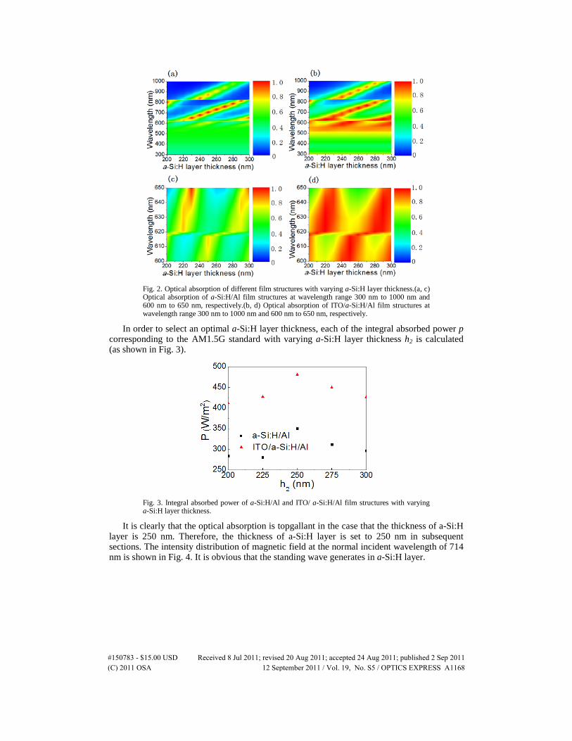
Fig. 2. Optical absorption of different film structures with varying a-Si:H layer thickness.(a, c) Optical absorption of a-Si:H/Al film structures at wavelength range 300 nm to 1000 nm and 600 nm to 650 nm, respectively.(b, d) Optical absorption of ITO/a-Si:H/Al film structures at wavelength range 300 nm to 1000 nm and 600 nm to 650 nm, respectively.
In order to select an optimal a-Si:H layer thickness, each of the integral absorbed power p corresponding to the AM1.5G standard with varying a-Si:H layer thickness h2 is calculated (as shown in Fig. 3).
Fig. 3. Integral absorbed power of a-Si:H/Al and ITO/ a-Si:H/Al film structures with varying a-Si:H layer thickness.
It is clearly that the optical absorption is topgallant in the case that the thickness of a-Si:H layer is 250 nm. Therefore, the thickness of a-Si:H layer is set to 250 nm in subsequent sections. The intensity distribution of magnetic field at the normal incident wavelength of 714 nm is shown in Fig. 4. It is obvious that the standing wave generates in a-Si:H layer.
#150783 - $15.00 USD Received 8 Jul 2011; revised 20 Aug 2011; accepted 24 Aug 2011; published 2 Sep 2011(C) 2011 OSA 12 September 2011 / Vol. 19, No. S5 / OPTICS EXPRESS A1168

Fig. 4. Normalized magnetic-field intensity distribution of a-Si:H thin film solar cell structure at the case of normal incidence, and the wavelengths is 714 nm.
3.2 Effect of nanoparticle sizes
In order to improve the absorption of a-Si:H solar cells, Al nanoparticles are embedded in ITO and the proposed structure is shown in Fig. 1 is utilized. Based on the discussion above, h1, h2, and h3 are respectively set to 100 nm, 250 nm and 100 nm. For the sake of simplicity,
xΛ and yΛ are fixed at 100 nm. The radius of nanoparticle changes from 10 nm to 50 nm. To investigate the effect of nanoparticals on the optical absorption clearly by the
comparison, it is an intuitive idea that the absorption enhancement factor used in this work is defined as the ratio of absorption of the same a-Si:H thin film solar cells with and without adding the Al nanoparticles. As shown in Fig. 5, the results show that remarkable absorption enhancement occurs in a few areas and the position of the enhanced absorption shifts to long wavelength with the increasing of nanoparticle radius. Adding Al nanoparticles into the basic cell structure can significantly improve the absorption at all short wavelengths. When the radius of nanoparticles is 30 nm, the absorption enhancement occurs almost throughout the wavelength range of interest and the absorption enhancement is remarkable in the short wavelength range.
Fig. 5. Mapping the absorption enhancement with varying structural parameters. For all nanoparticle-added cases, the nanoparticles are embedded in ITO. Absorption enhancement with both wavelength and nanoparticle radius. The other parameters h1, h2, h3 are 100 nm, 250 nm, 100 nm, respectively and the period
x yΛ = Λ = 100 nm.
After adding Al nanoparticles, the ITO layer can be seen as the superposition of two layers. Mathematically, it can be expressed as ' "
3 3 3h h h= + as shown in Fig. 6. The effective dielectric function of the "
3h layer is given by [16]:
#150783 - $15.00 USD Received 8 Jul 2011; revised 20 Aug 2011; accepted 24 Aug 2011; published 2 Sep 2011(C) 2011 OSA 12 September 2011 / Vol. 19, No. S5 / OPTICS EXPRESS A1169

, ,, ,
, , , ,
3 ( )1 ,
2 ( )r ITO r p
r eff r ITOr ITO r p r ITO r p
φ ε εε ε
ε ε φ ε ε
−= −
+ + − (3)
where ,r ITOε is the dielectric function of ITO, pr ,ε is the dielectric function of Al nanoparticle, ϕ is the particle volume fraction. It can be obtained that the effective dielectric permittivity of "
3h layer is larger than the pure ITO at the same wavelength.
Fig. 6. Cross-section view of ITO layer structure.
Therefore, the ITO layer with Al nanoparticles can be considered as a film of gradient refractive index between pure ITO and a-Si:H layer. It reduces the reflection of the a-Si:H layer and the absorption is increased. According to Mie’s scattering theory [17], the absorption and scattering cross section for such Al nanoparticles are expressed as:
[ ]2 Im ,absC π αλ
= (4)
3
24
8 ,3scaC π αλ
= (5)
where 34 ( / 1) / ( / 2)p e p erα π ε ε ε ε= − + is the polarizability of the particles. Here λ is the wavelength, r is the radius of the nanoparticles, pε is the wavelength-dependent complex dielectric function of the metal particles and eε is that of the embedding medium. Figure 7 shows the intensity distribution of magnetic field across of 30 nm Al nanoparticle in air and embedded in ITO of proposed structure, respectively. Here, the normal incident wavelength is set to 380 nm. Although the resonant frequency of Al lies outside the calculated wavelength range, the intensity of field around Al nanoparticle embedded in ITO is strengthened compared to nanoparticle in air. Such an enhanced absorption is mainly excited by the interaction between the internal structure and incident light.
Fig. 7. Magnetic-field intensity plots across Al nanoparticle (a) in air and (b) embedded in ITO of proposed structure.
#150783 - $15.00 USD Received 8 Jul 2011; revised 20 Aug 2011; accepted 24 Aug 2011; published 2 Sep 2011(C) 2011 OSA 12 September 2011 / Vol. 19, No. S5 / OPTICS EXPRESS A1170

It should be noted that the absorption of the proposed structure with Al nanoparticles is similar to that without nanoparticles in the long wavelength. However, the absorption peaks shift to long wavelength as shown in Fig. 8 for the changing of FP resonance wavelength. Therefore, the resonant wavelength in Eq. (2) should be modified as:
4
.2 1
effk
n dp
λ =−
(6)
The effective refractive index effn can be obtained from the numerical calculated reflection of the structure and it is slightly greater than n , which corresponds to the effective refractive index of the structure without Al nanoparticles. Therefore, the FP resonant wavelengths move little to long wavelength and they coincide with the curves in Fig. 8.
Fig. 8. Wavelength-dependent absorption of the structure with nanoparticles and without nanoparticles.
According to the above-mentioned discussions, it has been found that the optical absorption enhancement is remarkable when the radius is 30 nm and 50 nm. For a better view, wavelength-dependent absorption enhancement is shown in Fig. 9 for several cases of nanoparticle sizes of 10 nm, 20 nm, 30 nm, 40 nm and 50 nm. Throughout all of the curves, absorption enhancement of the structure with the nanoparticle radius of 30 nm is the perfect compared with the other four instances. Obviously, when nanoparticle radius is 50 nm, point 1 and 2, which correspond to two points in Fig. 5, denote intense absorption enhancement at the wavelength of 810 nm and 980 nm, respectively. However, the absorption is unsatisfactory in wavelength ranges of 500 nm to 800 nm and 820 nm to 920 nm. It is worth mentioning that too small nanoparticles almost have no effect on the optical absorption, for example the case of the nanoparticle of radius of 10 nm. Therefore, it is critical to select appropriate size of nanoparticle for the absorption enhancement.
Fig. 9. Wavelength-dependent absorption enhancement of a-Si:H thickness of 250 nm for different nanoparticle sizes of 10 nm, 20 nm, 30 nm, 40 nm and 50 nm.
#150783 - $15.00 USD Received 8 Jul 2011; revised 20 Aug 2011; accepted 24 Aug 2011; published 2 Sep 2011(C) 2011 OSA 12 September 2011 / Vol. 19, No. S5 / OPTICS EXPRESS A1171

In order to clearly illustrate variation of absorption with the radius of nanoparticles, each of the integral absorbed power p corresponding to the AM1.5G standard of the proposed structures with the nanoparticle of different radiuses r is calculated (as shown in Fig. 10). The result denotes a tendency that the integral absorbed power increases firstly and then decrease with the increasing of nanoparticle size. When the nanoparticle radius is of 30 nm, the absorption is greatest. For a single spherical particle [17], the incident light is intensively scattered or absorbed by the particle depending on the size of nanoparticles. The scattering is so weak that it is almost negligible when the size of the particle is too small and the structure can be seen as thin film structure. Oppositely, when the nanoparticle radius is too large, for example r = 50 nm, the surface coverage approaches 1. Therefore, the sunlight transmitting into the intrinsic absorption layer is greatly limited. The reflective energy is very strong and thus the absorption is not ideal.
Fig. 10. Integral absorbed power with varying nanoparticle radius.
3.3 Effect of nanoparticle position
For the investigation of the effect of nanoparticle position, a parameter h4, which characterizes the distance between the center of nanoparticles and the interface of a-Si:H and ITO is defined. Then the optical absorptions of the structures of different h4 are calculated and compared to obtain the effect of nanoparticle position on optical absorption. The results are shown in Fig. 11. When Al nanoparticles are away from the interface of a-Si:H and ITO, the light transmitting into a-Si:H layer is reduced gradually due to nanoparticles scattering and the light reflected by the interface is enhanced. Therefore, the absorption is reduced with the increasing of h4 in short wavelength range. When the distance between Al nanoparticles and the interface is large enough, the absorption is worse than that of the structure without Al nanoparticles. These results indicate that the absorption of Al nanoparticles is fairly weak and absorption enhancement of the proposed structure is mainly due to the scattering light of Al nanoparticles transmitting into a-Si:H layer and the absorption of a-Si:H layer is remarkably increased.
#150783 - $15.00 USD Received 8 Jul 2011; revised 20 Aug 2011; accepted 24 Aug 2011; published 2 Sep 2011(C) 2011 OSA 12 September 2011 / Vol. 19, No. S5 / OPTICS EXPRESS A1172

Fig. 11. Wavelength-dependent absorption with different embedded position of nanoparticles.
In order to highlight the advantages of this proposed structure, furthermore, three different structures, in which nanoparticles are placed at different positions,are analyzed, as shown in Fig. 12.
Fig. 12. Cross-sectional view of three structures. (a) Al nanoparticles at the surface of ITO. (b) Al nanoparticles embedded in the ITO and at the surface of a-Si:H layer at once. (c) Al nanoparticles embedded in a-Si:H layer.
It can be seen that absorption of proposed structure is the best of the three structures, which is plotted as a red dashed as shown in Fig. 13. For the structure shown in Fig. 12 (a), nanoparticle arrays can be treated as microcavities to trap incident light into the a-Si:H layer and increase the effective optical path length in the cell. For the third structure, as show in Fig. 12 (c), incident light is scattered by Al nanoparticles in existence and the effective absorption cross-section is increased. For the proposed structure in Fig. 12 (b), both of gradient refractive index structure effect and scattering effect play considerable roles in optical absorption enhancement.
#150783 - $15.00 USD Received 8 Jul 2011; revised 20 Aug 2011; accepted 24 Aug 2011; published 2 Sep 2011(C) 2011 OSA 12 September 2011 / Vol. 19, No. S5 / OPTICS EXPRESS A1173

Fig. 13. Wavelength-dependent absorption with different nanoparticle positions.
4. Conclusions
This paper has investigated the FP resonance of different film structures and optimized the thickness of a-Si:H layer. The optical absorption enhancement of a-Si:H thin film solar cells consisted of ITO layer with the array of nonresonant nanoparticles embedded in it and a-Si:H layer is verified and the oxidation of metallic nanoparticles can be avoided absolutely. The numerical calculated results have revealed that the absorption enhancement is remarkable in short wavelength for the optimal structure of a-Si:H thin film solar cells due to the scattering effect of Al nanoparticles. Simultaneously the proposed structure can be seen as gradient refractive index structure to restrain the reflection of the interface of ITO and a-Si:H thin film. Moreover, the different positions of nanoparticles have been taken into account. It is demonstrated that the optical absorption of the proposed structure is still topgallant.
Acknowledgment
This work is financially supported by the National Natural Science Foundation of China (Grant No.50936002).
#150783 - $15.00 USD Received 8 Jul 2011; revised 20 Aug 2011; accepted 24 Aug 2011; published 2 Sep 2011(C) 2011 OSA 12 September 2011 / Vol. 19, No. S5 / OPTICS EXPRESS A1174