efficient control of igbt transistor as part of
TRANSCRIPT

International Journal of Electrical Engineering and Computing Vol. 1, No. 1 (2017)
46
Original research paper UDC 621.382.33:621.314.57
DOI 10.7251/IJEEC1701046J
COBISS.RS-ID 7196952
Efficient Control of IGBT Transistor as Part of Overvoltage Protection
Nenad Jovančić, Nijaz Hadžimejlić, Pero Ćeklić
R&D department, KV Team, Sarajevo, Bosnia and Herzegovina (in cooperation with DV Power, Sweden)
nenad.j, nijaz.h, [email protected]
Abstract - The paper analyzes the phenomena of appearance of overvoltage during the switching-off of the IGBT transistor which are caused by the presence of parasitic inductance in the switching circuit. This problem can be solved in two ways – by preventing the cause of the overvoltage, or by limiting the overvoltage level. Therefore, the characteristics of good PCB design have been noted, and the typical snubber’s circuits have been listed. The paper focuses on solving the problem of IGBT transistor overvoltages on a specific power electronics converter. A computerized model of power electronics converter has been created in order to analyze the influence of parasitic inductance on the overvoltage level. A special analysis was performed on the simulation results which indicate that the control of the IGBT transistor turning-off process can provide a lower overvoltage level. The paper also describes the design and the implementation of the overvoltage protection elements on a developed power electronics converter prototype. The driver circuit TD350 which performs intelligent control of IGBT transistors in order to control overvoltages has been described in detail. The efficiency of this driver is based on the idea of two-level turn-off, where the intermediate level and its duration can be set according to the specific conditions in the IGBT transistor circuit. This way, the speed of current change is reduced, which directly affects the overvoltage level on the transistor switching. Finally, within experimental results, the waveforms of control signals, as well as the overvoltage waveforms have been shown at different input voltage levels.
Keywords - component; parasitic inductance; overvoltage protection; power converter; IGBT.
I. INTRODUCTION
Nowadays, it is difficult to imagine an electronic device
without any power electronic converters. Each converter
contains at least one switching element (electronic switch)
which has a key role in its operation. This means that the
reliability and efficiency of the electronic device is directly
dependent on the reliable and efficient operation of the
switching element.
When selecting the switch, it is important to make sure that
its characteristics such as nominal current and voltage satisfy
the current and voltage characteristics of its environment. In
addition to the nominal value of the electrical element
parameters, each of them always includes, to a lesser or greater
extent, the parasitic components from other elements. Their
presence usually negatively effects the operation of the system.
This paper will discuss the influence of parasitic components
on the appearance of overvoltage on switching elements, which
can seriously influence their reliability and operational
efficiency. The major methods for the overvoltage suppression
will be listed. Finally, a specific method of overvoltage
protection of IGBT transistors based on the TD350 control
circuit will be presented.
II. PARASITIC INDUCTANCE AND ITS INFLUENCE ON
OVERVOLTAGE ON SWITCHING ELEMENTS
In schematic diagram, the connections between electronic
components are represented as ideal conductors – without any
resistance, inductance or capacitance. However, this is
frequently not the case in practice, because the connections are
normally made of materials with finite conductance (such as
copper, aluminum, platinum, silver, gold...). Also, their surface,
shape and mutual positioning determines the size of inductance
and/or capacitance between them. Since these values are
usually very low and their influence is usually negative, they
are frequently called “parasitic”. For example, the parasitic
inductance of copper on the PCB layer with 70 µm thickness,
35 mm length and 10 mm width, is around 20 nH [1].
During the turn-off period, the energy accumulated in
parasitic inductances (LP), through which a current is flowing,
that the switch needs to interrupt, will be released, which leads
to the appearance of an overvoltage over the switch. The
This paper is a revised and expanded version of the paper presented at the
XVI International Symposium INFOTEH-JAHORINA 2017 [9]. Corespondence to: N. Jovančić ([email protected])
In cooperation with DV Power (www.dv-power.com), Sweden
International Journal of Electrical Engineering and Computing Vol. 1, No. 1 (2017)
47
overvoltage magnitude is directly proportional to the amount of
accumulated energy in the parasitic inductance and the turn-off
time (1).
V(t)=LP∙di/dt (1)
The overvoltage formed in this manner has sufficient energy
to permanently damage the switch and / or generate
electromagnetic interference, which makes it very important to
limit or completely eliminate their occurrences while designing
the converter.
III. THE METHODS FOR PREVENTING AND LIMITING THE
OVERVOLTAGE IN POWER CONVERTERS
While designing the overvoltage protection, one needs to be
aware of the overvoltage causes, whose function is mentioned
in the previous paragraph with equation (1). This paper will
demonstrate how the reduction of parasitic components
(primarily inductance) and intelligent control of the switch
operation can reduce the overvoltage which formed during turn-
off period.
The reduction of parasitic components is accomplished by
properly designing the connections between the converter
elements – PCB layout design. This means that the connections
should be as short as possible. Also, the surface of the loop
formed by reactive and switching elements should be as small
as possible.
While selecting the method for the switching control, care
must be taken. Reducting the switching speed will reduce the
overvoltage. However, this will also increase the switch loss,
due to increase of transition time between ON and OFF state
(turn-off period). Additional losses require additional cooling,
which makes the design more costly [2, 3].
There are many designs available in the market which
provide intelligent control algorithms and which keep the
overvoltage and switch losses within the desired boundaries.
One such design was used for this paper, which will be
additionally discussed.
In addition to the methods for preventing the cause of their
appearance, there are additional methods for reducing the
existing overvoltage, where some of the switching losses energy
is dissipated on snubbers or returned towards the energy source.
There have been many attempts to derive universal classification
scheme for snubbers. The problem is the many different function
performed by circuits which are called “snubbers”. In general,
such schemes haven’t been particularly useful but for the
purposes of this article, snubbers will be grouped with similar
characteristics. None of these distinctions are very rigorous, but
are convenient to subdivide the discussion [4].
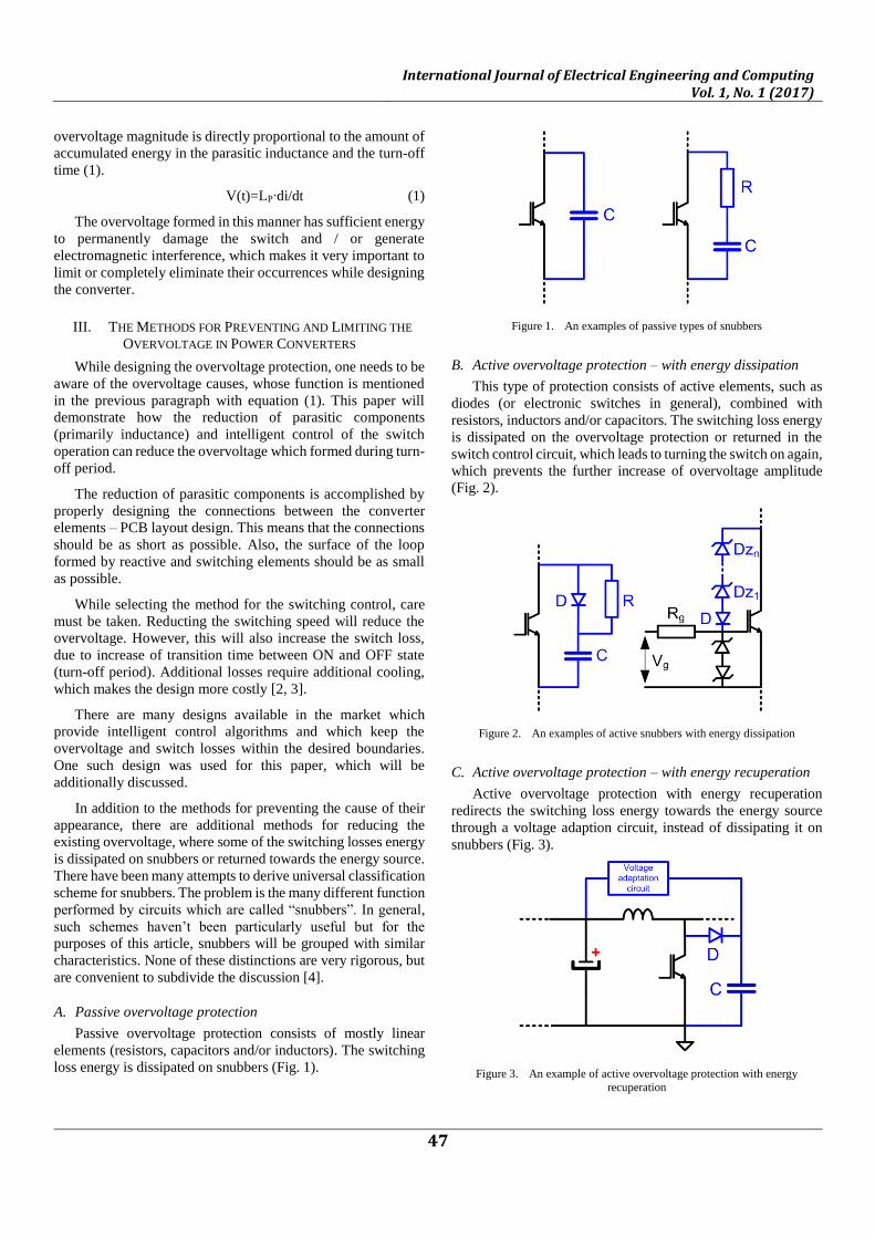
A. Passive overvoltage protection
Passive overvoltage protection consists of mostly linear
elements (resistors, capacitors and/or inductors). The switching
loss energy is dissipated on snubbers (Fig. 1).
Figure 1. An examples of passive types of snubbers
B. Active overvoltage protection – with energy dissipation
This type of protection consists of active elements, such as
diodes (or electronic switches in general), combined with
resistors, inductors and/or capacitors. The switching loss energy
is dissipated on the overvoltage protection or returned in the
switch control circuit, which leads to turning the switch on again,
which prevents the further increase of overvoltage amplitude
(Fig. 2).
Figure 2. An examples of active snubbers with energy dissipation
C. Active overvoltage protection – with energy recuperation
Active overvoltage protection with energy recuperation
redirects the switching loss energy towards the energy source
through a voltage adaption circuit, instead of dissipating it on
snubbers (Fig. 3).
Figure 3. An example of active overvoltage protection with energy
recuperation

Nenad Jovančić et al.
48
IV. AN EXAMPLE OF REALIZATION OF EFFICIENT
OVERVOLTAGE PROTECTION OF IGBT TRANSISTORS
Due to their robustness (capability of withstand high current
and voltage stress) and ease of control, IGBT transistors are
frequently used as switches in power converters with high rated
power (tens or even hundreds of kilowatts). An efficient method
of protecting IGBT transistors from overvoltage effects, based
on a combination of passive and active types of overvoltage
protection and intelligent control, will be demonstrated on an
example of a power converter, which will be described in detail.
A. The Power Converter Structure and IGBT Transistor
Operating Conditions
The power converter which is the subject of this paper
represents the central part of the electronic load system used to
simulate a purely resistive programmable load. Its basic
structure is very simple (Fig. 4).
Figure 4. Schematic of electronic load
A filter at the input, consisting of Lf inductance and Cf
capacitor, provides continuous current from the source Uu. The
element which dissipates most of the power is a resistive tape
placed in a spiral. As such, in addition to its resistance R, the
tape also has inductance – parasitic inductance LR. The current
regulation is performed using an IGBT transistor T, which
operates in a switching mode. The entire electronic load system
is designed to operate with voltage of up to 500 VDC and
maximum power of up to 25 kW.
B. The Computer Model of the Converter
Due to the need to analyze the influence of parasitic
inductances of connections between the transistor and
associated converter elements on the appearance of
overvoltage, a computer model has been created (Fig. 5) with
real models of individual elements of the converter (which
include parasitic values of resistance, capacitance and
inductance). The parameters of the individual elements are
modeled based on the manufacturer's catalog data. Furthermore,
the parasitic inductances of the resistive tape (LR) as well as
parasitic inductances (LV) and resistances (RV) of copper on the
PCB lines were measured using a RLC meter SANWA-
LRC700.
The results of the simulation provide answers to two
different questions: how do the parasitic inductances of the PCB
lines affect the distribution of overvoltage between specific
points on the converter, and the influence of turn-off process
control on the overvoltage level. The results which will be
presented and analyzed were obtained with the following
simulation parameters: Uin=480 VDC, Iin=60 A, fsw=20 kHz,
gate turn-on and turn-off voltage Ug1=15 VDC i Ug2=-9 VDC,
respectively. Considering the approximation (2), which describe
dependence between turn-off time Tf and turn-off gate current
Igoff, where the parameter Qg represent the total gate charge
(listed by the transistor manufacturer), the change of turn-off
time Tf has been simulated using the change of turn-off gate
current Igoff.
Tf≈Qg/Igoff (2)
Figure 5. Computer model of the power converter (created in OrCAD)
C1
330u
IC = 440
R1
0.110
00
Lv2
Rv1
Rv2
DC snubber - clamp
C2
1u
IC = 440
0
L6
5nH
1 2
L7
5nH
1
21/2 Parasiticinductance andresistance ofPCB lines
Resistive tape
RC snubber
Input LC filter
R18
10u
Lrc1 30nH
1
2
Rrc1
4R7
R21
2k2
V1
480
R11
0.01m
BZX84C18/ZTX
D7
BZX84C12/ZTX
D9
Lp2
30nH
1
2
Rp2
0.01m
L1
30uH
1 2
R5
4.1
0
D10
D1N4448
Rof f 1
10R
Freewheel diode
Parasitic inductance and resistance ofwires between Cc and Cin
Rv 1
6m
Lv 1
80nH
LC1
12nH
1
2
D6
DSEP29-12A
21
Parasiticinductanceof tape
Lt1
5uH
1 2
V2
TD = 0
TF = 2uPW = 30uPER = 50u
V1 = -9
TR = 0.01u
V2 = 15
0
Ron1
10R
1
2
3
Crc1
3n3
Dc
0
Cc
LR
Lv1
Lp1
30nH
1
2
Rp1
0.01m
R9
2m
LC2
12nH
1
2
C4330u
IC = 440
1/2 Parasiticinductance andresistance ofPCB lines
R2
0.110
Cin
0
M1
IXXKX200N65B4

International Journal of Electrical Engineering and Computing Vol. 1, No. 1 (2017)
49
1) Influence of parasitic inductance of PCB lines on the
distribution of overvoltage. The connection of the collector of
IGBT transistor with the DC diode consists of two parts in the
models – the part between collector (point 1 in Fig. 5) and the
resistor RRC1 (point 2 in Fig. 5) has been modeled using a
resistance (RV1=10 uΩ) and parasitic inductance (LV1=30 nH).
Furthermore, the part between point 2 and the anode of the DC
diode (point 3 in Fig. 5) has also been modeled using a resistance
(RV2=10 uΩ) and parasitic inductance (LV2=30 nH).
The Fig. 6 shows the voltage waveforms in points 1, 2 and 3,
in case of transistor turn-off time of Tf=100 ns. It is easy to
notice that the overvoltage has the highest value on the collector
of IGBT transistor (points 1). This shows that the overvoltage
level, for same turn-off time, is directly related to the magnitude
of the parasitic inductance which exists in the lines between
switching element and the other elements of the power
converter.
Figure 6. Influence of parasitic inductances on the overvoltage distribution
(Tf=100 ns)
2) The influence of transistor turn-off process control on
the overvoltage level. The Fig. 7 shows the voltage waveforms
in the three characteristic points (1, 2 and 3) under the same
conditions as in the previous test, with the transistor turn-off
time increased from 100 ns to 2 µs. In the point 3, the
overvoltage level is effectively unchanged. However, the
overvoltage in other points has been significantly reduced. In the
point 2 the overvoltage has been reduced by 38 V (6,5%), while
in the point 1 the overvoltage has been reduced by as much as
57 V (8,7%).
Figure 7. The influence of the transistor turn-off time on the overvoltage
level (Tf=2 µs)
Since the overvoltage level depends on the rate of change of
transistor current (equation (1)) and based on the obtained
simulation results, it is possible to conclude that controlling of
the turn-off process of the transistor can influence the level of
overvoltage in the moment of switching it off.
Considering the fact that the transistor parasitic capacitance
between the gate and the emitter CGE and between the gate and
the collector CGC (Miller’s capacitance), which determine the Qg
parameter, are non-linear, in other words that the depend on the
circuit conditions, specifically the collector-emiter (VCE) and
gate-emiter (VGE) voltage, the detail mathematical relations
between Tf and overvotage level ΔUCE is a complex subject and
has not been covered in detail in this paper. More details can be
found in literature [5] and [6].
Due to the non-linearity of the function ΔUCE =f(Tf), which
is the consequence of existence of parasitic capacitance CGE and
CGC and the phenomena of their charging/discharging, an
intelligent control method is required in order to control level of
ΔUCE effectively [7].
For the purpose of driving the IGBT transistor of the
developed converter that is the subject of this paper, a TD350
driver has been used, which will be discussed in more detail
below.
C. Realisation of inteligent driving of IGBT – integrated circuit
TD350.
The TD350 device is an advanced gate driver for IGBTs and
power MOSFETs. Control and protection functions are included
and allow the design of high reliability systems. The innovative
active Miller clamp function eliminates the need for negative
gate drive in most applications and allows the use of a simple
bootstrap supply for the high side driver (Fig. 8).
The device includes a two-level turn-off feature with
adjustable level and delay. This function protects against
excessive overvoltage at turn-off in case of overcurrent or short-
circuit conditions. The same delay set in the two-level turn-off
feature is applied at turn-on to prevent pulse width distortion.
The device also includes IGBT desaturation protection and a
FAULT status output, and is compatible with both pulse
transformer and optocoupler signals. [8]
Figure 8. Functional block diagram [8]
The input (IN) is compatible with optocouplers or pulse
transformers. The input is triggered by the signal edge and
allows the use of a small-sized, low cost pulse transformer. Input
is active low (output is high when input is low) to ease the use
of the optocoupler. When driven by a pulse transformer, the
input pulse (positive and negative) width must be larger than the
minimum pulse width tonmin.

Nenad Jovančić et al.
50
Desaturation protection (DSAT) ensures the protection of
the IGBT in the event of overcurrent. When the DESAT voltage
goes higher than 7 V, the output is driven low (with 2-level turn-
off, if applicable). The FAULT output is activated. The FAULT
state is exited at the next falling edge of IN input. A
programmable blanking time is used to allow enough time for
IGBT saturation.
A Miller clamp allows the control of the Miller current
during a high dV/dt situation and can eliminate the need for a
negative supply voltage. During turn-off, the gate voltage is
monitored and the clamp output is activated when gate voltage
goes below 2 V (relative to GND). The clamp voltage is VL+3
V max. for a Miller current up to 500 mA. The clamp is disabled
when the IN input is triggered again.
The two-level turn-off (TLTF) is used to increase the
reliability of the application. In the event of a short-circuit or
over-current in the load, a large voltage overshoot can occur
across the IGBT at turn-off and can exceed the IGBT breakdown
voltage. By reducing the gate voltage before turn-off, the IGBT
current is limited and the potential over-voltage is reduced. This
technique is called a two-level turn-off (TLTF). Both the level
and duration of the intermediate off-level are adjustable.
Duration is set by an external resistor/capacitor in conjunction
with the integrated voltage reference for accurate timing. The
level can be easily set by an external Zener diode, and its value
is selected depending on the IGBT characteristics. This TLTF
sequence takes place at each cycle; it has no effect if the current
does not exceed the normal maximum-rated value, but protects
the IGBT in case of over-current (with a slight increase of
conduction losses) [8].
This principle is shown in Fig. 9. During the TLTF time, the
OUTL output is controlled by a comparator between the actual
OUTL pin and an external reference voltage. When the voltage
on OUTL goes down as a result of the turn-off and reach the
reference threshold, then the OUTL output is disabled and the
IGBT gate is not discharged further. After the TLTF delay, the
OUTL output is enabled again to end the turn-off sequence.
Figure 9. Principle schematic for two-level turn-off fetaure
The duration of the TLTF is set by the external RC
components, and is given by (3):
Ta[μs]≈0.7∙Roff[kΩ] Coff[nF] (3)
To keep the output signal width unchanged relative to the
input signal, the turn-on is delayed by the same value as the
TLTF delay.
Minimum ON time. In order to ensure the proper operation
of the 2-level turn-off function, the input ON time (Twin) must be
greater than the Twinmin value (4):
Twinmin[μs]=Ta[μs] + 2∙Rdel[kΩ] Coff[nF] (4)
Rdel is the internal discharge resistor and Coff is the external
timing capacitor. Input signals smaller than Ta are ignored. Input
signals larger than Twinmin are transmitted to the output stage
after the Ta delay with minimum width distortion (5).
(∆Tw = Twout - Twin) (5)
For an input signal width Twin between Ta and Twinmin, the
output width Twout is reduced below Twin (pulse distortion) and
the IGBT could be partially turned on. These input signals should
be avoided during normal operation.
The output stage is able to sink 2.3 A and source 1.5 A
(typ.) at 25 °C (1.2 A/0.75 A minimum over the full temperature
range). Separate sink and source outputs allow independent gate
charge and discharge control without an extra external diode.
Undervoltage detection protects the application in the event
of a low VH supply voltage (during startup or a fault situation).
During undervoltage, the OUTH pin is open and the OUTL pin
is driven low. Fault output signals the undervoltage state and is
reset only when undervoltage state disappears.
D. Results Obtained on the Developed Converter Prototype
Based on the knowledge obtained from theory of causes and
effects of overvoltage in power converters, as well as the
analysis of the simulated model results, a converter prototype
has been developed whose diagram, with the elements of
overvoltage protection, is shown in Fig. 10.
Figure 10. Schematic diagram of developed converter prototype with the
elements of overvoltage protection
Due to the parasitic inductance of the resistive tape (LR≈5
µH), an overvoltage protection of IGBT transistor has been
formed as a combination of active (DC-CC) and passive (RRC-
CRC) overvoltage protection. Due to presence of parasitic
inductances (LV≈60 nH) of connections between the IGBT
transistor and its surroundings and strict requirement for
overvoltage level, additional measures were necessary to reduce
overvoltage to an acceptable level – specifically, intelligent
transistor driving.

International Journal of Electrical Engineering and Computing Vol. 1, No. 1 (2017)
51
The driving of IGBT transistor was performed by the TD350
control circuit. The TLTF function is configured in the following
manner: turn-on voltage level VH=15 VDC, turn-off voltage
level VL=-9 VDC, turn-off delay time Ta=2 µs and the
intermediate off-level LVOFF =2.5 V. The full waveform of
realized driving signal of the IGBT transistor has been shown in
Fig. 11.
Figure 11. Achived TLTF control signal waveform
The Fig. 12 shows a part of the PCB of the developed
converter prototype. The marked sections show the positions of
the IGBT transistor and the overvoltage protection elements.
Figure 12. Developed converter prototype – the positions of the IGBT
transistor and the overvoltage protection
As seen in the Fig. 12, the elements have been positioned in
such a way to reduce the connection lines length to a minimum.
This also reduces the parasitic inductances of these connections.
Also, the marked points 1, 2 and 3 are the voltage measurement
points discussed during the simulation results analysis (Fig. 6
and Fig. 7). The next section will provide an overview and
result analysis from the developed converter prototype.
In the IGBT transistor voltage waveform (UCE) at Uul=480
VDC and Iul=60 A, shown in Fig. 13, it is possible to see that the
overvoltage, shown as a thin “spike” is practically gone. The
only visible part is the muffled sinewave oscillation whose
frequency matches the resonant frequency of the passive part of
overvoltage protection – RC snubber.
Figure 13. Waveform UCE (CH1) and Iin (CH2) at Uin=480 VDC
For the sake of comparison, Fig. 14 shows the voltage
waveform UCE with the turn-off time TfA=100 ns (without
TLTF) and TfB=2 µs (with TLTF). In both cases, the values of
input voltage and current were Uin=300 VDC and Iin=70 A.
(a)
(b)
Figure 14. Voltage waveforms UCE without TLTF (a) and with TLTF (b)

Nenad Jovančić et al.
52
There is an obvious difference between the overvoltage
levels for these two cases. Without TLTF and for TfA=100 ns,
the maximum value of the UCE voltage is 440 V, while with
TLTF and for TfB=2 us, the maximum voltage value is
significantly lower and amounts to 350 V.
The demonstrated experimental results are a clear indicator
that the switching elements in power converters can be provided
with operating conditions which guarantee reliability and
efficiency in both normal and fault conditions with a proper
design of overvoltage protection. This implies that during
designing process, attention should be paid to the:
- minimization of parasitic elements of converters (PCB
layout design),
- design of overvoltage protection elements and
- optimal choise of control system for switching elements.
V. CONCLUSION
While developing power converters, one needs to consider
the causes of appearance and negative effects of parasitic
inductances which can affect the reliability and efficiency of
switching elements which are often key parts of the converter.
The basic principles of the appearance and limiting of the
overvoltage influence on the converter operation were shown in
the paper. Special attention was devoted to the intelligent
transistor control as an efficient method of overvoltage
prevention. An example of application of specially designed
control circuit which reduces overvoltage by slowing down the
transistor OFF time was demonstrated. The provided results,
obtained using a simulation and experimental measurements on
the developed converter prototype, show that a combination of
active and passive overvoltage protection, together with
intelligent control, can provide an efficient overvoltage
protection to the IGBT transistor.
REFERENCES
[1] Chemandy Electronics, [Online]. Available at: http://chemandy.com/calculators/flat-wire-inductor-calculator.htm.
[2] W.-s. Choi, D.-k. Son, M. Hallenberg, “Driving and Layout Design for Fast Switching Super-Junction MOSFETs“, HV PCIA PSS Team, Fairchild Semiconductor, ON Semiconductor, [Online]. Available at: www.onsemi.com, 2013.
[3] L. Balogh, Fundamentals of MOSFET and IGBT Gate Driver Circuits, Texas Instruments – Application report, SLUA618-March 2017 – Revised SLUP169 – April 2002
[4] R. Severns, „Snubber Circuits for Power Electronics“, 2008.
[5] Y. Zhang, S. Sobhani, R. Chokhawala, “Snubber Considerations for IGBT Applications” International Rectifier Applications Engineering, 233 Kansas St., El Segundo, CA, 90245 USA
[6] A. Volke, M. Hornkamp, “IGBT Modules – Technologies, Driver and Application“, Infineon Technologies AG, Munich, Second edition 2012.
[7] ST Microelectronics, „Advanced IGBT/MOSFET driver“ DocID018539 Rev 3, 2013
[8] STMicroelectronics, “Developing IGBT applications using an TD350 advanced IGBT driver”, Application note AN1944, October 2006.
[9] N. Jovančić, N. Hadžimejlić, P. Ćeklić, “Efikasno upravljanje IGBT tranzistora upotrebom TD350 integralnog kola”, INFOTEH-Jahorina, vol. 16, pp. 1-5, 2017.
Nenad Jovančić received the B.S., and
M.S. degrees in 2009 and 2013, from the
University of East Sarajevo, Faculty of
Electrical Engineering. Since 2009 he
works as R&D engineer in KV Team,
Sarajevo (in cooperation with DV
Power, Sweden). The company
develops and manufactures electronics
and industrial automation systems. His
research interests are in power supply
units, systems for battery testing and power electronics in
general. He is the author or the co-author of several technical
papers.
Nijaz Hadžimejlić received the B.S.,
M.S. and Ph.D. degrees in 1977, 1987
and 1997, from the University of
Sarajevo, all in electrical engineering.
From 1977 to 1998 he was with the
Department of Power Electronics and
Motor Control, of the Institute for
Computer Science and Control-IRCA,
Energoinvest, Sarajevo. From 1984 to
1997 he worked part time as Teaching
Assistant and Senior Teaching Assistant
at the Department Of Electrical
Engineering, University of Sarajevo. He joined the Department
Of Electrical Engineering, University of Sarajevo from 1998 till
2016 as the Associate Professor. He is additionaly engaged as a
consultant to KV Team and DV Power company, and from
2016 he joined full time with KV Team company. His research
interests are in power electronics converters, motor drive
control for electrical cars and robotics. He is the author or the
co-author of over fifty technical papers.
Pero Ćeklić received the M.S. degree in
2005, from University of East Sarajevo,
Faculty of Electrical Engineering
(automatics and electronisc). Since
2006 he works as R&D engineer in KV
Team, Sarajevo (in cooperation with
DV Power, Sweden). The company
develops and manufactures electronics
and industrial automation systems. His
research interests are in power supply
units, systems for power and measurement transformers testing
and power electronics in general. He is the author or the co-
author of several technical papers.