effects of sio2 and tio2 nano fillers in enhancing the...
TRANSCRIPT

Effects of SiO2 and TiO2 Nano Fillers in Enhancing the Insulation Breakdown Strength of Epoxy Nano Composite Dielectric under
Divergent Electric Fields
S. Mohamed Ghouse1, S. Venkatesh2, R.Rajesh3, and S. Natarajan4
1,2,4Department of Electrical and Electronics Engineering, School of Electrical and Electronics Engineering, SASTRA University, Thanjavur, 613401, India. 3 Srinivasan Engineering College, Perambalur, 621212, India.
[email protected] , [email protected] , [email protected], [email protected]
Abstract: The proper mixing of nanoscale fillers in conventional dielectric materials leads to an enhancement in the breakdown strength and voltage endurance. In this study experimental investigations are carried out to compare the breakdown characteristics of epoxy nano-composites with that of a base epoxy resin under the influence of divergent electric fields so as to obtain inferences on its breakdown performances. This would in turn enable providing solutions to acquire more effective electrical insulation systems and explore the prospect of tapping the merits of utilizing the rapid strides made in field of fabrication of nano-dielectrics. The main objective is such studies are to enhance the electrical properties of the epoxy dielectric by employing nano-fillers such as SiO2, TiO2 etc. This research envisages the use of epoxy resin mixed with nano-fillers for ascertaining the ability of the nano-composite to be utilized as a dielectric/ insulator in power apparatus. The epoxy resin is mixed with appropriate proportion of SiO2 and TiO2 and experimentation is carried out under the influence of divergent electric fields. Classical breakdown voltage withstand tests such as AC power frequency, DC voltage, lightning impulse and switching impulse test is carried out on epoxy dielectrics (with and without nano-fillers) and the results are compared. In addition, a non-classical breakdown voltage test (high frequency high voltage) is also devised to analyze and ascertain the breakdown characteristics due to varying frequencies so as to investigate the possibility of utilizing such nano-composites in applications related to high speed switching devices. Keywords: Epoxy resin, nano-fillers, Divergent electric fields
1. Introduction In the field of power systems design, installation and operation, electrical insulation plays a major role. In recent years several high voltage application systems utilizes Epoxy based insulating materials with different operating conditions. The epoxy dielectric materials are frequently exposed to huge electrical stresses and during long run the dielectric will degrade and shorten the life span of the equipment. Hence the need of the hour is to develop insulating materials for High voltage electrical applications with better electrical and mechanical characteristics. The research article by Lewis [1], discusses the introduction of nano fillers in the dielectric material in enhancing the electrical and mechanical properties of the nano composite insulation. Further, improved manufacturing techniques due to the advent of nano-technology has resulted in renewal of focus among researchers to explore on the possibility of developing stronger yet compact dielectric/ insulation system pertaining to power apparatus. The research studies reported by Tanaka et. al., [2],[3], in the development of polymer nanocomposites shows the improvement in the electrical properties of the new class of nano dielectric materials.
Received: October 24th, 2013. Accepted: December 5th, 2013
International Journal on Electrical Engineering and Informatics - Volume 5, Number 4, December 2013
501

In this context, nano-dielectrics has emerged as new area in high voltage engineering which aims at development of a new class of insulation materials with improved mechanical and electrical properties which could have substantial commercial implications [3]-[4]. This aspect becomes all the more relevant, since cost of insulation is a substantial portion of the net cost of the power system. Hence, attempts to provide solutions for obtaining higher dielectric withstand strength (by mixing nano-fillers with the base polymer unlike the conventionally used bulk expensive fillers) at reduced cost [5]-[7] has become the main focus of challenge to researchers worldwide. The use of nano-fillers instead of its expensive polymer-filler counterpart has proved to be most efficient in terms of cost and electrical performance. Further, failures reported in composite insulation system of large power apparatus attribute breakdown due to chemical, thermal and mechanical aspects also as precursors to electrical insulation collapse due to purely electrical stresses. The addition of nano-fillers has been found to improve the mechanical and chemical property. In this research the main objective is to test epoxy resin based dielectric under divergent electric fields and assess its dielectric breakdown strength and comparing the same with epoxy resin dispersed with SiO2 and TiO2 nano-fillers. In most of the cases, failure of electrical insulation is often followed by the failure in mechanical and thermal property of the insulator. By adding the nano-fillers it is proposed that the mechanical strength as well as the thermal strength of the insulator increases. Increase in the aforementioned two properties ensures durability of the insulator i.e., even with less volume the insulator can with stand very high transmission voltages [8]. Hence, detailed studies and substantial analysis of insulation system comprising nano-fillers may provide innovative solutions to insulation system in a variety of applications such as outdoor insulators, switchgears, DC cables, electrochemical capacitors, and insulation for inverter-fed motors etc. 2. Epoxy Nano-composite Preparation Methodology In this work first a mould of thickness 2mm is made using galvanized iron sheet. Epoxy resin [Poly(Bisphenol A- co-Epichlorohydrin)] of suitable quantity is taken in a glass beaker. The beaker containing the epoxy resin is heated by maintaining a temperature of 45°C in a hot plate apparatus. Due to the oxidation of the phenolic compound, the final product obtained becomes black in colour in the form of gel. This indicates the complete formation of the epoxy resin. Nano-fillers are added to 5% of the base (epoxy resin) material’s weight. The complete dispersion of the nanofillers can be ensured by using a high speed mixer. Once the fillers are thoroughly dispersed, Triethylenetetramine (TETA) is added to the solution as a hardener, so that the resulting polymer is heavily cross-linked, and is thus rigid and strong. The prepared sample is poured into the mould without lowering the temperature of 45°C as epoxy is a thermosetting resin and hardens as soon as the temperature falls below the preparing temperature. Air bubbles appearing on the surface is removed by applying heat on the surface
Figure 1. Preparation of Epoxy Nano-dielectric
using a blow torch. The prepared sample is allowed to cool for the duration of 10 minutes. Fast cooling of the sample is avoided to make the sample less brittle.[9]-[14]. Figure. 1 shows the various stages of preparation of the epoxy nano-dielectric.
S. Mohamed Ghouse, et al.
502
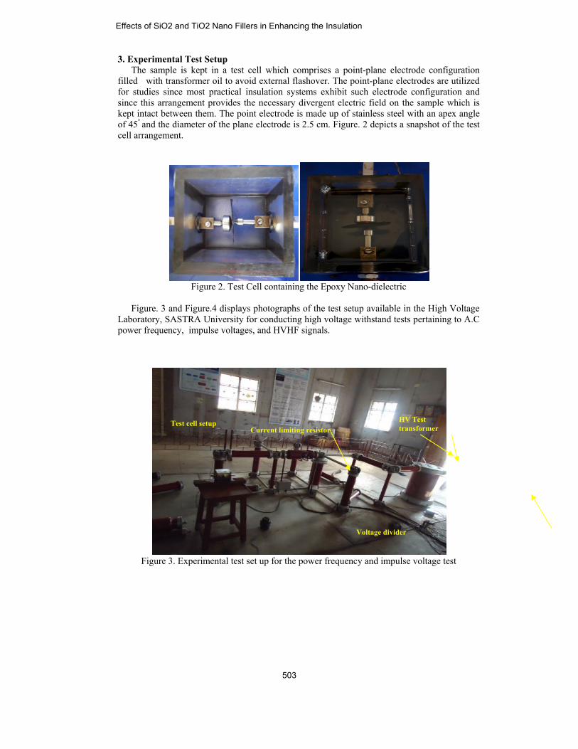
3. Experimental Test Setup The sample is kept in a test cell which comprises a point-plane electrode configuration filled with transformer oil to avoid external flashover. The point-plane electrodes are utilized for studies since most practical insulation systems exhibit such electrode configuration and since this arrangement provides the necessary divergent electric field on the sample which is kept intact between them. The point electrode is made up of stainless steel with an apex angle of 45° and the diameter of the plane electrode is 2.5 cm. Figure. 2 depicts a snapshot of the test cell arrangement.
Figure 2. Test Cell containing the Epoxy Nano-dielectric
Figure. 3 and Figure.4 displays photographs of the test setup available in the High Voltage Laboratory, SASTRA University for conducting high voltage withstand tests pertaining to A.C power frequency, impulse voltages, and HVHF signals.
Figure 3. Experimental test set up for the power frequency and impulse voltage test
HV Test transformer Current limiting resistor
Test cell setup
Voltage divider
Effects of SiO2 and TiO2 Nano Fillers in Enhancing the Insulation
503

Figure 4. Experimental test set up for the High Voltage High Frequency test
4. Power Frequency and Impulse Voltage Test Setup For the purpose of comparison, studies are carried out to determine the breakdown characteristics during classical test procedures namely the power frequency and impulse (lightning and switching) voltage setup. The power frequency voltage test setup utilizes a high voltage test transformer tunable to 100kV with appropriate voltage divider for further measurement and acquisition of waveforms. Figure 5 depict a typical test setup of the power frequency voltage test setup utilized during studies.
Test Cell Setup
Capacitive
Voltage Divider
Current Limiting
Resistor
DSO
Measuring Cable
Epoxy NanoComposite
HV Test Transformer10 kVA, 0-230V/ 0-100 kV Figure 5. Power Frequency Test Setup for Epoxy didelectric Insulation Testing
A single stage Marx Impulse Voltage generator arrangement is setup to carry out impulse voltage testing due to the classical lightning (1.2/50 µs) and switching (250/2500 µs) transients. The test setup comprises a set of sphere gaps, a charging capacitor and appropriately chosen wave-shaping components for obtaining the standard lightning and switching wave shapes. Figure 6 indicates the Marx impulse generator circuit arrangement utilized for carrying out impulse studies on Epoxy dielectric samples.
S. Mohamed Ghouse, et al.
504

Figure 6. Experimental Test Setup for Impulse Voltage Breakdown Studies
HVTest Transformer 10kVA, 50Hz, (0-230V/0-100kV)
140kV PIV Diode Unit 140kV PIV Diode Unit 10MΩ
Earth Switch
Controllable Sphere Gap
25000pF
1200pf
TestCell
280 MΩ Potential divider
AC Servo Motor
LI Voltage R1= 245Ω/140kV R2= 2400Ω/140kV SI Voltage R1=43kΩ/ 140kV R2=48kΩ/140kV
Support Insulation rod
R1
R2
Quadrapole
Effects of SiO2 and TiO2 Nano Fillers in Enhancing the Insulation
505
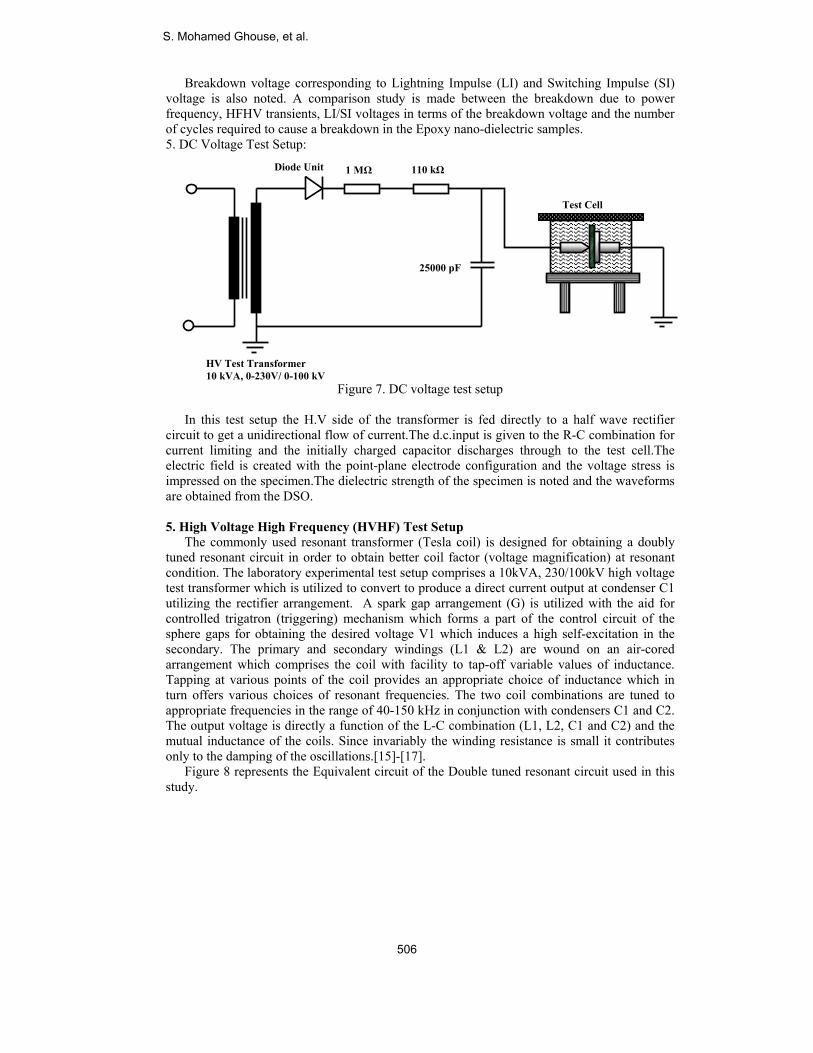
Breakdown voltage corresponding to Lightning Impulse (LI) and Switching Impulse (SI) voltage is also noted. A comparison study is made between the breakdown due to power frequency, HFHV transients, LI/SI voltages in terms of the breakdown voltage and the number of cycles required to cause a breakdown in the Epoxy nano-dielectric samples. 5. DC Voltage Test Setup:
Figure 7. DC voltage test setup
In this test setup the H.V side of the transformer is fed directly to a half wave rectifier circuit to get a unidirectional flow of current.The d.c.input is given to the R-C combination for current limiting and the initially charged capacitor discharges through to the test cell.The electric field is created with the point-plane electrode configuration and the voltage stress is impressed on the specimen.The dielectric strength of the specimen is noted and the waveforms are obtained from the DSO. 5. High Voltage High Frequency (HVHF) Test Setup The commonly used resonant transformer (Tesla coil) is designed for obtaining a doubly tuned resonant circuit in order to obtain better coil factor (voltage magnification) at resonant condition. The laboratory experimental test setup comprises a 10kVA, 230/100kV high voltage test transformer which is utilized to convert to produce a direct current output at condenser C1 utilizing the rectifier arrangement. A spark gap arrangement (G) is utilized with the aid for controlled trigatron (triggering) mechanism which forms a part of the control circuit of the sphere gaps for obtaining the desired voltage V1 which induces a high self-excitation in the secondary. The primary and secondary windings (L1 & L2) are wound on an air-cored arrangement which comprises the coil with facility to tap-off variable values of inductance. Tapping at various points of the coil provides an appropriate choice of inductance which in turn offers various choices of resonant frequencies. The two coil combinations are tuned to appropriate frequencies in the range of 40-150 kHz in conjunction with condensers C1 and C2. The output voltage is directly a function of the L-C combination (L1, L2, C1 and C2) and the mutual inductance of the coils. Since invariably the winding resistance is small it contributes only to the damping of the oscillations.[15]-[17]. Figure 8 represents the Equivalent circuit of the Double tuned resonant circuit used in this study.
Test Cell
25000 pF
Diode Unit 1 MΩ 110 kΩ
HV Test Transformer 10 kVA, 0-230V/ 0-100 kV
S. Mohamed Ghouse, et al.
506

Figure 9 represents the typical HVHF signal generated using the proposed circuit.
Rg
C1
L1, R1 C2
L2, R2
E0
Eg
Figure 8. Equivalent Circuit
Figure 9. Typical HVHF Waveform from DSO
The primary and secondary circuits resonate at the same frequency, ωr which is given by The corresponding Equations for the primary and secondary circuit can be written as 0 At resonance both primary and secondary coils behave as purely resistive circuit. Hence at resonance 0 and 0
Effects of SiO2 and TiO2 Nano Fillers in Enhancing the Insulation
507

The equation for secondary current and output voltage at resonance can be written as: Secondary current at resonance
Output voltage at resonance
Figure 10 illustrates a typical layout of the double tuned test setup utilized for HVHF testing of epoxy nano-dielectric.
HV Test Transformer 10kVA, 0 -230V/0 -100kV
Automatic Earth Switch To DSO
Test Cell
200MVA, 140 kV PIV Diode Unit
Controllable Sp here gap10 MΩ, 140kV
200MΩ, 140kV
R1
R2L1
L2
C2Cm
C1
Figure 10. Typical Layout of Double Tuned Resonant Test Setup
Test set up comprises a tuned high frequency resonant oscillator, divider, measuring impedance connected to a 200 MHz, 200 MS/s DSO (DL 1620®). The selected range of high frequencies for the experiment varies from (40–115) kHz.[16] and [17]. This range has been selected since researchers who have carried out HFHV studies on similar such studies have chosen a comparable range of frequencies since a few reported incidents of failures has been observed to occurred at such frequencies[18],[19] and [20]. 7. Comparison & Analysis of the Influence of Nano-fillers in Epoxy Resin Initially high voltage 50Hz power frequency is applied on the epoxy resin without nano-filler and 5 samples are tested for dielectric breakdown test and the calculated average breakdown strength is observed to be 66.3 kV. Power frequency voltage at 50Hz is also applied on the epoxy resin with TiO2 nano-fillers and Epoxy resin with SiO2& TiO2 nano-fillers and the calculated average breakdown strength is 76.5kV and 86.8 kV respectively. From the breakdown values it is evident that the addition of nano-fillers increases the dielectric strength of the material. Table 1 depicts the breakdown values of the samples tested under AC power frequency.
Table 1. High Voltage AC Power Frequency Voltage Breakdown Test
Test Samples Break down strength(kV) Sample 1 Sample 2 Sample 3 Sample 4 Sample 5
Epoxy resin without nanofillers
64.3 kV 65.7 kV 66.2 kV 68 kV 67.3 kV
Epoxy resin with TiO2 nanofillers 74.4 kV 76.3 kV 75.5 kV 79 kV 77.5 kV
Epoxy resin with Sio2& Tio2 nanofillers
81.4 kV 83.7 kV 88.2 kV 91.3 kV 89.7 kV
S. Mohamed Ghouse, et al.
508

Figure 11. Comparison of Breakdown strength of Epoxy resin with and without Nanofillers
under A.C Power frequency
A similar procedure is adopted for the DC voltage breakdown test. The average values of the breakdown strength of the epoxy resin without nano-filler, with TiO2 nano-filler, with TiO2 and SiO2 nano-filler are observed to be 89.2kV, 101.1kV and 106.2 kV respectively. Hence the DC voltage withstanding capability of the nano-dielectric is higher than the AC voltage withstanding capability which may be attributed to frequency independent characteristic of polarization during DC testing. Table 2 depicts the various breakdown values of the samples tested under high voltage DC.
Table 2. High Voltage D.C. Voltage Breakdown Test
Test Samples Breakdown Strength (kV) Sample 1 Sample 2 Sample 3 Sample 4 Sample 5
Epoxy resin without nanofillers
85.6 kV 88.2 kV 91.6 kV 90.8 kV 89.9 kV
Epoxy resin with TiO2 nanofillers 101.5 kV 93.6 kV 103.8 kV 104.5 kV 102.3 kV
Epoxy resin with Sio2& Tio2 nanofillers
105.7 kV 106.2 kV 102.5 kV 108.8 kV 107.9 kV
Figure 12. Comparison of Breakdown strength of Epoxy resin with and without Nanofillers
under High voltage D.C
Effects of SiO2 and TiO2 Nano Fillers in Enhancing the Insulation
509

The prepared sample is also subjected to LI and SI breakdown tests. During lightning impulse test the average values of the breakdown strength of the epoxy resin without nano-filler, with TiO2 nano-filler, with TiO2 and SiO2 nano-filler are found to be 74.4 kV, 85.3kV and 94.5kV respectively. During switching impulse test the average values of the breakdown strength of the epoxy resin without nano filler, with TiO2 nano-filler, with TiO2 and SiO2 nano-filler are found to be 123.5kV, 124.2kV and 131.4kV respectively. The nano-dielectric hence withstands higher voltages during SI when compared to LI. Table 3 and Table 4 depicts the various breakdown values of the samples tested under lightning and switching over voltages.
Table 3. Lightning Impulse Voltage Breakdown Test
Test Samples Break down strength (kV) Sample 1 Sample 2 Sample 3 Sample 4 Sample 5
Epoxy resin without nanofillers
73.7 kV 74.2 kV 74.9 kV 73.8 kV 75.6 kV
Epoxy resin with TiO2 nanofillers
84.6kV 85.3kV 86.7kV 84.8kV 85.3kV
Epoxy resin with SiO2& TiO2 nanofillers
94.6kV 92.8kV 93.4kV 95.4kV 96.6kV
Figure 13. Comparison of Breakdown strength of Epoxy resin with and
without Nanofillers under Lightning Impulse voltage
Table 4. Switching Impulse Voltage Breakdown Test
Test Samples Break down strength (kV) Sample 1 Sample 2 Sample 3 Sample 4 Sample 5
Epoxy resin without nanofillers 124.6 kV 119.2 kV 125.1 kV 120.3 kV 128.7 kV
Epoxy resin with TiO2 nanofillers 124.6 kV 123.7 kV 122.6 kV 123.7 kV 126.4 kV
Epoxy resin with Sio2 & Tio2 nanofillers
128.6 kV 129.4 kV 135.8 kV 130.9 kV 132.3 kV
S. Mohamed Ghouse, et al.
510

Table 5. High Frequency High Voltage (HFHV) Breakdown Test
Frequency of HFHV Transients
Double Tuned Circuit Parameters
Test Sample
Breakdown Strength kV
Parameters of Primary
Circuit
Parameters of Secondary
Circuit Sample 1 Sample 2 Sample 3
43kHz
C1= 51200pF (25000pF||
25000pF||1200pF)
L1= 0.265mH
C2=1300pF (1200pF||100p
F)
L2= 10.10 mH
Epoxy resin without
nanofillers 72.2kV 71.6kV 70.3kV
Epoxy resin with TiO2 nanofillers
83.4kV 84.5kV 80.5kV
Epoxy resin with SiO2&
TiO2 nanofillers 95.3kV 97.5kV 93.6kV
60kHz C1= 25000pF
L1= 0.265mH
C2 =2500pF (1200pF
||1200pF|| 100 pF)
L2= 2.9 mH
Epoxy resin without
nanofillers 51.5kV 55.6kV 53.4kV
Epoxy resin with TiO2 nanofillers
63.4kV 67.5kV 66.3kV
Epoxy resin with SiO2&
TiO2 nanofillers 72.4kV 70.2kV 74.5kV
86 kHz
C1= 26200pF
(25000pF|| 1200pF)
L1= 0.134mH
C2 =1200pF L2= 2.83 mH
Epoxy resin
without nanofillers
78.4kV
76.4kV
76.4kV
Epoxy resin with TiO2 nanofillers
84.4kV 85.7kV 88.4kV
Epoxy resin with SiO2&
TiO2 nanofillers 95.6kV 93.2kV 99.4kV
111kHz
C1= 13700pF (12500pF|| 1200pF)
L1= 0.14 mH
C2 =1200pF L2= 1.7 mH
Epoxy resin without
nanofillers 141kV 142.5kV 143.6kV
Epoxy resin with TiO2 nanofillers
144.2kV 144.4kV 146.5kV
Epoxy resin with SiO2&
TiO2 nanofillers 148.1kV 146.3kV 147.3kV
Effects of SiO2 and TiO2 Nano Fillers in Enhancing the Insulation
511

Figure 14. Comparison of Breakdown strength of Epoxy resin with and without Nanofillers
under Switching Impulse voltage
Repetitive HFHV transients are applied and the specimens are observed for breakdown. If breakdown occurs, corresponding breakdown voltage for a particular frequency is noted else voltage is increased by 0.5kV. Table 5 depicts the studies conducted for epoxy nano-dielectric samples for wide range of HVHF transients.
Figure 15. Comparison of Breakdown strength at 43kHz and 60kHz HFHV signal
S. Mohamed Ghouse, et al.
512

Figure 16. Comparison of Breakdown strength at 86 kHz and 111 kHz HFHV signal
Figure 17. Frequency Vs Average Breakdown strength characteristics
In Zone I the Breakdown strength of the dielectric decreases with increase in frequency due to influence of volume charges and dielectric loss effect. It is also to be noted that the dielectric loss is a function of frequency (P=V2fCtanδ). As the frequency increases the voltage
I II
II
Effects of SiO2 and TiO2 Nano Fillers in Enhancing the Insulation
513

required fmay be du In Zonincreases voltage in This arequired idielectric which are
F
for breakdownue to dipole spne II and Zone
as random vncreases as the aspect is also cin this zone (R
at higher freqe recorded in D
Figure 18. Brea
n decreases duinning at differ
e III the virtualvelocity compo
frequency incrconcurred by r
Region 5) indicquencies. Figu
DSO during LI,
akdown voltage
ue to thermal arent frequenciel distances of tonent increasereases in these esearchers as dated in [21] to
ure 18 and Fig SI and HVHF
e at 43kHz and
agitation causees. travel for free es with freque
zones. deliberated in explore the ph
gure 19 showsF testing.
d 60 kHz HVH
ed at higher fr
electrons betwency. Hence t
[21]. Further ihysical behavios the breakdow
HF Signals from
requency. This
ween electrodesthe breakdown
investigation isor of the nano-wn waveforms
m DSO
s
s n
s -s
S. Mohamed Ghouse, et al.
514

Thus insulator fillers notepoxy insa lesser vo 6. Conclu The epto that of
Figure 19. Bre
from the abovmaterial incre
t only increasessulators designoltage when co
usions poxy resin mixthe base epoxy
eakdown voltag
ve observationseases its electrs the electrical ed without nanompared to the
xed with nano-y specimen. Th
ge at Lightning
s it is evident trical propertiesproperties but
no-fillers are foe nano-compos
-filler has betthe interfacial p
g and Switchin
that the use ofs considerablyt also increasesound to be mucite epoxy insul
er dielectric brproperties have
ng Impulse volt
f nano-fillers my. The additions its mechanicach brittle and blators.
reakdown strene to be taken ca
tages
mixed with then of the nano-al strength. Thebreaks down at
ngth comparedare of which is
e -e t
d s
Effects of SiO2 and TiO2 Nano Fillers in Enhancing the Insulation
515

facilitated by preparing the specimen & the quantity of the filler in calculated quantities, which plays a dominant role in deciding the dielectric behavior and the molecular configuration of the specimen. The test values obtained make it evident that the specimen could sustain more overvoltage, particularly lightning surges and may be stressed with additional overvoltage with better characteristics. The power frequency test results show that the specimen has better voltage endurance characteristics and the addition of nano-fillers has proved to be effective. Thus, it can be inferred that the nano-composite fabricated is effective and may serve as a plausible insulating material for power apparatus. Though further detailed studies may be essential to validate the possibility of utilizing these nano-composite materials it is envisaged by the authors of this research to take up future studies to carry out thorough studies to ascertain the possibility of fabricating and manufacturing power devices such as outdoor insulators, switches, tripping circuits etc. 7. Acknowledgement The authors of this work are extremely grateful to Prof.R. Sethuraman, Vice-Chancellor, SASTRA University, Dr. S. Vaidhyasubramaniam, Dean-Planning and Development, SASTRA University and Dr. S. Swaminathan, Dean-Sponsored Research and Director- CeNTAB, SASTRA University for the unwavering support and motivation extended to them during the course of the research. The authors are also grateful to Dr. B. Viswanathan, Dean/SEEE, SASTRA University for many useful suggestions, discussion and motivation. 8. References [1] T. J. Lewis, “Nanometric Dielectrics”, IEEE Trans. Dielectr. Electr. Insul., Vol.1, pp.
812-825, 1994. [2] T. Tanaka, G. C. Montanari, G. Mulhaupt, “Polymer Nanocomposites as Dielectrics and
Electrical Insulation–Prospective for Processing Technologies, Material Characterization and Future Applications”, IEEE Trans. Dielectr. Electr. Insul., Vol.11, No.5, 2004, pp.763-784.
[3] T. Tanaka, 2005, “Dielectric Nanocomposites with Insulating properties”, IEEE Trans. Dielectr. Electr. Insul, Vol. 12, pp. 914-928.
[4] J. K. Nelson, J. C. Fothergill, L. A. Dissado and W. Peasgood, 2002, “Towards an Understanding of Nanometric Dielectrics”, IEEE Conf. Electr. Insul. Dielectr. Phenomena (CEIDP), pp. 295-298
[5] M. Kozako, N. Fuse, Y. Ohki, T. Okamoto and T. Tanaka, “Surface Degradation of Polyamide Nanocomposites Caused by Partial Discharges Using IEC(b) Electrodes”, IEEE Trans. Dielectr. Electr. Insul.,Vol.11, No.5, 2004, pp.833-839.
[6] T. Imai, Y. Hirano, H. Hirai, S. Kojima and T. Shimizu, 2002, ‘‘Preparation and Properties of Epoxy- organically Modified Layered Silicate Nanocomposites’’, IEEE Intern. Sympos. Electr. Insul. ISEI., pp. 379-383.
[7] T. Tanaka, G. C. Montanari and R. Mulhaupt, 2004, “Polymer Nanocomposites as Dielectrics and Electrical Insulation - Perspectives for processing Technologies, Material Characterization and Future Applications”, IEEE Trans. Dielectr. Electr. Insul, Vol. 11, pp. 763-784.
[8] T. Sels, J. Karas et al, 2002, “Electrical Insulation Behaviour Subject to Fast Transients using a Tesla Transformer” , 6th International Multi-Conference on Power and Energy Systems (IASTED), PES 2002, Marina Del Rey, California.
[9] J. K. Nelson and Y. Hu, 2003, ‘‘Electrical Properties of TiO2 nanocomposites, IEEE Conf. Electr. Insul. Dielectr. Phenomena CEIDP., pp. 19-722.
[10] C. Zilg, D. Kaempfer, R. Muelhaupt and G. C. Montanari, 2003, ‘‘Electrical Properties of Polymer Nanocomposites Based upon Organophilic Layered Silicates’’, IEEE Conf. Electr. Insul. Dielectr. Phenomena CEIDP., pp. 546-550.
S. Mohamed Ghouse, et al.
516

[11] B. KA TuApp
[12] MarLice
[13] P. MwithMon
[14] K. EInsuConfChin
[15] S. VInveDouICES
[16] ElanInsuConfChin
[17] Hardand Symp
[18] SelsTranand
[19] Vanin Tof 151.12
[20] Vanof FPES
[21] Chau
Karthikeyan, R.uned Circuit Alications of Di
rco Denicolai, 2entiate Thesis,
Mohaupt, M. Gah Variable Freqntreal. Elanseralathan, ulating Materiaference on Prona.
Venkatesh, S. Mestigation on Inuble Tuned CircS-2012, Septem
nseralathan, K.ulating Materiaference on Prona. dt, N. and D. Khigh Voltage bposium on Ele, T., J. Karas e
nsients using a Energy System
n Cranenbroeckransformers an5th Internation
2.6. n Cranenbroeckast Transient P
S Winter Meetinurasia, M P, "H
S. MElectrMaste2006.in thElectrarea o
. Rajesh, S. VeApproach”, 8th I
electric Materi2001, “Tesla THelsinki Univeamlin et al, 199quency”, E1-85
Joy Thomas als Under High
operties and Ap
Mohamed Ghounsulation Integrcuit Techniquember 14-15. , Joy Thomas als Under High
operties and Ap
Koenig, 1998, based on the Teectrical Insulatiet al., 2002, “ETesla Transfor
ms (IASTED), Pk, T., H. De Hend Substations nal Conference
k, T., H De HerPhenomena in Dng, Singapore.High Voltage E
Mohamed Ghronics Engineeer Degree in P. He is a membe Department rical Electroniof interest inclu
enkatesh, S. SaInternational Cials, pp. 380 –
Transformer forersity. May 3097, “High Volt5, Internationa
and G. R. NagaFrequency Vo
pplications of D
use, and S. Narity of XLPE Ce”, Internationa
and G. R. NagaFrequency Vo
pplications of D
“Testing of Insesla Transformion, pp. 517-52
Electrical Insularmer”. 6th Inter
PES 2002, Marerdt et al., 1999Leading to an
e on Electricity
rdt et al., 2000,Distribution Tr
Engineering", K
house obtainedering from Bh
Power system Eber of IEEE an
of Electrical cs Engineeringudes composite
arvanan, 2006, Conference on 383.
r Experimentat. tage Testing Ul Symposium o
abushana, 2000oltage Stress”, Dielectric Mat
atarajan, , 2012Cables Due to Hal Conference
abushana, 2000oltage Stress”. Dielectric Mat
sulating Matermer Principle”, 20. ation Behaviournational Multrina Del Rey, C9,“Detailed StuImproved Sys
y Distribution (
, “Experimentaransformers”. P
Khanna Publish
d his Bacheloharathidasan UEngineering frnd presently wo
and Electrong, SASTRA Ue dielectric sys
“Dielectric IntProperties and
tion and Resea
Using Series Reon High Voltag
0, “Breakdown6th Internation
terials (ICPAD
2, “ExperimentHVHF Transieon Electrical S
0, “Breakdown6th Internation
terials (ICPAD
ials at High FrIEEE Internat
ur Subject to Fti-Conference oCalifornia. udy of Transientem Design”. P
(ICRED 1999),
al and NumericProceedings of
hers, 2nd editio
or Degree in University, Indi
om Annamalaiorking as Assinics Engineerin
University, Indistem and Nano
tegrity Test d
arch” ,
esonance ge (ISH 97),
of Solid al
DM 2000),
tal ents Using Sciences
n of Solid al
DM 2000),
requencies tional
ast on Power
nt Phenomena Proceedings 1.12.1-
cal Analysis f the IEEE
on, 2000.
Electrical andia in 2001 andi University instant Professorng, School ofia. His specificdielectrics.
d d n r f c
Effects of SiO2 and TiO2 Nano Fillers in Enhancing the Insulation
517

Assistant ElectricalpublicatiosuccessfuHe is alsoinclude PRecognitiInsulation
monitorin
Current AconditionComputat
S.VenEnginTechnLater EnginPatterAlstoMana
Professor in l and Electronons to his crully completed o a reviewer inPartial Discharion and Artifin Society and S
R. EngDegUniDepEnginclRes
ng of dielectric
S. NEnginDegrUnivElectProfeSchoIndia
Analysis, Fren monitoring otional Intellige
nkatesh obtainneering from Anology-High V
he received neering specialrn Recognitionm Limited, Sy
ager- Engineerthe Departmenics Engineerinedit in Interna Research &
n leading Internrge, Substationcial Intelligen
Smart Grid Com
Rajesh obtaigineering fromgree in Techiversity in 20partment of Elgineering Colllude Polarsponse Analys systems in tra
Natarajan obtaneering from ree in Technolversity in 2006trical and Elecessor in the Dool of Electrica. His specifiquency Respo
of dielectric syence Society.
ned his BacheAnnamalai UnivVoltage Enginehis Ph.D. frolizing in the fn Using Moduystems Group-Iring & Qualitnt of Electricang, SASTRA Unational Journ
Modernizationnational Journn Engineeringce. He is an mmunity.
ined his Bachem Bharathidasahnology-High 003. He is lectronics and ege Perambalurization Deposis, Partial D
ansformers.
ained his BachBharathidasan
logy-Computer6. He was ectronics EnginDepartment ofcal and Electric areas of inonse Analysisystems in trans
elor Degree inversity, India ineering from SAm SASTRA U
field of Multipular Neural NeIndia, T & D Pty Assurance.al and ElectronUniversity, Indals and Confn Fund (R & M
nal publishers. g & EHV Traactive membe
elor Degree inan University,
Voltage Enpresently woCommunicati
ur, India. Hiolarization CuDischarge Ana
helor Degree in University, r Science and earlier with JKneer. He is pref Electrical anronics Enginee
nterest include s, Partial Discsformers. He i
n Electrical ann 1994 and MaASTRA UniveUniversity in ple Source Paretworks. He warojects Divisio He is presenics Engineeridia. He has seferences of reMF) project in His specific aransmission syer of IEEE, IE
n Electrical an India in 199
ngineering froorking as Proions Engineeriis specific areurrent Analysalysis related
in Electrical anIndia in 199Engineering f
K Pharmachemesently workinnd Electronicsering, SASTRPolarization D
charge Analyis a member o
nd Electronicsaster Degree inersity in 2004High Voltage
rtial Dischargeas earlier with
on, as Assistantently a Senioring, School ofeveral researchepute. He hasthe year 2011
reas of intereststems, Pattern
EEE Dielectric
nd Electronics93 and Masterom SASTRAofessor in theng, Srinivasaneas of interestis, Frequency
to condition
nd Electronics3 and Master
from SASTRAm Limited, asng as Assistants Engineering,
RA University,Depolarization
ysis related toof IEEE, IEEE
s n . e e h t r f h s . t n c
s r
A e n t y n
s r
A s t , ,
n o E
S. Mohamed Ghouse, et al.
518