effective fabrication of three-dimensional nano/microstructures in a single step using multilayered...
TRANSCRIPT

Effective fabrication of three-dimensional nano/microstructures in a single step usingmultilayered stampSang-Hu Park, Tae-Woo Lim, Dong-Yol Yang, Jun-Ho Jeong, Ki-Don Kim, Kwang-Sup Lee, and Hong-Jin Kong Citation: Applied Physics Letters 88, 203105 (2006); doi: 10.1063/1.2204448 View online: http://dx.doi.org/10.1063/1.2204448 View Table of Contents: http://scitation.aip.org/content/aip/journal/apl/88/20?ver=pdfcov Published by the AIP Publishing Articles you may be interested in Fabrication of a large, ordered, three-dimensional nanocup array Appl. Phys. Lett. 101, 081109 (2012); 10.1063/1.4747464 Adaptive bonding technique for precise assembly of three-dimensional microstructures Appl. Phys. Lett. 90, 233109 (2007); 10.1063/1.2746085 Multiple level nanochannels fabricated using reversal UV nanoimprint J. Vac. Sci. Technol. B 24, 2984 (2006); 10.1116/1.2393247 Submicron three-dimensional structures fabricated by reverse contact UV nanoimprint lithographya) J. Vac. Sci. Technol. B 24, 3002 (2006); 10.1116/1.2388962 Three-dimensional polymer structures fabricated by reversal ultraviolet-curing imprint lithography J. Vac. Sci. Technol. B 23, 2954 (2005); 10.1116/1.2130349
This article is copyrighted as indicated in the article. Reuse of AIP content is subject to the terms at: http://scitation.aip.org/termsconditions. Downloaded to IP: 193.0.65.67
On: Sat, 22 Nov 2014 13:07:12

Effective fabrication of three-dimensional nano/microstructuresin a single step using multilayered stamp
Sang-Hu Park, Tae-Woo Lim, and Dong-Yol Yanga�
Department of Mechanical Engineering, Korea Advanced Institute of Science and Technology,Daejeon 305-701, Korea
Jun-Ho Jeong and Ki-Don KimNano-Mechanical Systems Research Center, Korea Institute of Machinery and Materials,Daejeon 305-343, Korea
Kwang-Sup LeeDepartment of Polymer Science and Engineering, Hannam University, Daejeon 306-791, Korea
Hong-Jin KongDepartment of Physics, Korea Advanced Institute of Science and Technology, Daejeon 305-701, Korea
�Received 10 February 2006; accepted 18 April 2006; published online 15 May 2006�
A technique in ultraviolet nanoimprint lithography �UV-NIL� for the creation of three-dimensional�3D� nanopatterns in a single step is proposed. The single-step fabrication of 3D or multilevelstructures has a multitude of benefits. Inherent in this is the elimination of a need for alignment formultilevel fabrications as well as being a cost effective and simple process. For 3D UV-NIL, a trialin the fabrication of multilayered stamps has been conducted employing two-photon polymerizationand diamondlike carbon �DLC� coating technique. The DLC coating layer enables the polymerpatterns to be used effectively as a stamp without the need for an antiadhesion material.Additionally, O2-plasma ashing has the potential for an epoch-making improvement of the precisionof polymer patterns with a linewidth of 60 nm. Overall, several fine patterns are imprinted using themultilayered stamp onto a UV-curable resist via a single-step process without any identifiabledamage. © 2006 American Institute of Physics. �DOI: 10.1063/1.2204448�
Nanoimprint lithography �NIL� is known as an emerginglithography with a resolution of less than 10 nm, having ahigh throughput and low cost compared to the conventionalphotolithography.1–5 In ultraviolet �UV� NIL, a nanopat-terned UV-transparent stamp is pressed onto a spin-coatedresin on a substrate and then cured by UV light.3 This pro-cess demands only a low pressing pressure and can be doneat room temperature, which has some advantages comparedto the thermal-type NIL. Until now, most of the researchworks concerned with NIL are focused on two-dimensional�2D� patterning for mass production. However, the fabrica-tion of three-dimensional �3D� nano/microstructures is ofgreat importance in diverse fields of modern technology forthe development of highly functional applications. From thispoint of view, some 3D nano/microfabrication techniqueshave been developed using nonphotolithographic ap-proaches. Among them, two-photon polymerization �TPP� isconsidered as a promising technique and has been exten-sively studied over the last decade in order to fabricate com-plex 3D micro/nanodevices by a method of stackinglayers.6–14 TPP is considered currently as a unique techniquethat could create a real 3D microstructure with a high spatialresolution beneath the limit of diffraction of light. More de-tailed explanations on TPP are given in numerous reports.8–14
However, a high processing time is normally required to cre-ate 3D microstructures due to the intrinsic TPP characteristicof the layer-by-layer accumulation. For this reason, TPP isevaluated as an incongruent process for mass production in
spite of its unique capability of complete 3D micro- andnanoscale fabrications. Therefore, in being the latest, the in-crease of throughput in TPP becomes an important issue forits practical use as a nanofabrication process.15–17
In this work, the fabrication process of a 3D multilay-ered stamp besides, applicable to UV-NIL and has a resolu-tion of sub-100-nm scale, is introduced for the fabrication of3D or multilevel nano/microstructures in a single-step. Thesingle-step fabrication of multilevel structures has somemeaningful advantages of avoiding an alignment issue ofseveral 2D stamps �or masks� including the low fabricationcost due to a single stamp and a simple process. Figure 1summarizes the fabrication procedure of the 3D multilayeredstamp for UV-NIL, which consists of four different parts: aglass plate, polymer patterns, a diamondlike carbon �DLC�layer, and a thick glass plate for reinforcement. On a thinglass plate, 3D polymer patterns were created using TPP. Forthis work, an optical femtosecond laser system has been uti-lized. The full specifications on the developed system weregiven in our previous reports.8–10,12 Through these proce-dures, 3D polymer patterns on the thin glass plate were cre-ated for use as an UV-NIL stamp with the advantages of aflexible design, as well as being perfectly transparent to UVlight.
Another important issue concerned with TPP that comesinto being in recent research works is how to improve theresolution of microstructures. In general, it is well knownthat the resolution in TPP is dependent on the process param-eters such as laser power and exposing time. The previousworks have shown that the high spatial resolution of a voxelcould be achieved with a delicate control of the laser dose
a�Author to whom correspondence should be addressed; elecronic mail:[email protected]
APPLIED PHYSICS LETTERS 88, 203105 �2006�
0003-6951/2006/88�20�/203105/3/$23.00 © 2006 American Institute of Physics88, 203105-1 This article is copyrighted as indicated in the article. Reuse of AIP content is subject to the terms at: http://scitation.aip.org/termsconditions. Downloaded to IP: 193.0.65.67
On: Sat, 22 Nov 2014 13:07:12
into the near-threshold energy region for polymerization.7–10
Moreover, an approach using a radical quencher to improvethe resolution of a voxel has been reported in a recentstudy,18 in which a lateral spatial resolution of 100 nm wasachieved using the quenching effect. However, in case thequenching effect is utilized, the mechanical strength of thepolymerized structure is inevitably reduced, despite achiev-ing a high spatial resolution, because of the smaller molecu-lar weight of polymerized structures.19 Therefore, a challeng-ing issue related with the enhancement of the mechanicalstrength still remains when it comes to the practical use ofradical quenchers in the 3D nanofabrication.
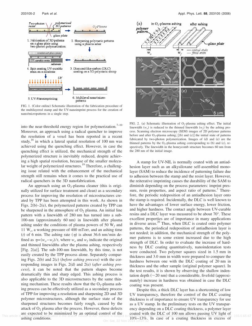
An approach using an O2-plasma cleaner �this is origi-nally utilized for surface treatment and clean� as a secondaryprocess for improving the resolution of microstructures cre-ated by TPP has been attempted in this work. As shown inFigs. 2�b�–2�e�, the polymerized patterns created by TPP canbe sharpened in the atmosphere of O2 plasma. An initial linepattern with a linewidth of 280 nm has turned into a sub-100-nm �approximately 60 nm� in linewidth after plasmaashing under the conditions of plasma powers of 50 W f and11 Wr, a working pressure of 400 mTorr, and an ashing time�t� of 6 min. The ashing rate ��� is about 36.6 nm/min de-fined as �= �wo−wf� / t, where wo and wf indicate the originaland thinned linewidths after the plasma ashing, respectively�Fig. 2�a��. The sub-100-nm linewidth, by this time, is noteasily created by the TPP process alone. Separately compar-ing Figs. 2�b� and 2�c� �before ashing process� with the cor-responding images in Figs. 2�d� and 2�e� �after ashing pro-cess�, it can be noted that the pattern shapes becomedramatically thin and sharp edged. This ashing process isalso applicable to the 3D microstructures by the same thin-ning mechanism. These results show that the O2-plasma ash-ing process can be effectively utilized as a secondary processof TPP for improving a resolution and sharpening 2D and 3Dpolymer microstructures, although the surface state of thesharpened structures becomes fairly rough, caused by theattack of O2 plasma after the process. However, these defectsare expected to be minimized by an optimal control of theashing conditions.
A stamp for UV-NIL is normally coated with an antiad-hesion layer such as an alkysiloxane self-assembled mono-layer �SAM� to reduce the incidence of patterning failure dueto adhesion between the stamp and the resist layer. However,the reiterative imprinting causes the durability of the SAM todiminish depending on the process parameters: imprint pres-sure, resin properties, and aspect ratio of patterns.3 There-fore, the periodic redeposition of an antiadhesion layer ontothe stamp is required. Incidentally, the DLC is well known tohave the advantages of lower surface energy, lower friction,and higher hardness. The contact angle between UV-curableresins and a DLC layer was measured to be about 70°. Theseexcellent properties are of importance in many applicationsin diverse areas.20 Thus, when DLC is coated onto polymerpatterns, the periodical redeposition of antiadhesion layer isnot needed; in addition, the mechanical strength of the poly-mer patterns is to some extent increased due to the highstrength of DLC. In order to evaluate the increase of hard-ness by DLC coating quantitatively, nanoindentation testswere conducted. Two polymer squares sized in 1.5 mm inthickness and 3.0 mm in width were prepared to compare thehardness between one with the DLC coating of 20 nm inthickness and the other sample �original polymer square�. Inthe test results, it is shown by observing the shallow inden-tation depth ��20 nm� that a considerable, fivefold �approxi-mately� increase in hardness was obtained in case the DLCcoating was present.
Despite this, a thick DLC layer has a shortcoming of lowUV transparency, therefore the control of the DLC coatingthickness is of importance to ensure UV transparency for useas a UV stamp. In the preliminary tests on the UV transpar-ency depending on a DLC coating thickness, a polymer layercoated with the DLC of 100 nm allows passing UV light of10%–13%. In case of a coating thickness in excess of
FIG. 1. �Color online� Schematic illustration of the fabrication procedure ofthe multilayered stamp and the UV-nanoimprint process for the creation ofnano/micropatterns in a single step.
FIG. 2. �a� Schematic illustration of O2-plasma ashing effect. The initiallinewidth �wo� is reduced to the thinned linewidth �wf� by the ashing pro-cess. Scanning electron microscopy �SEM� images of 2D polymer patternsbefore and after O2-plasma ashing; ��b� and �c�� the initial state of patternsfabricated by two-photon polymerization. Images of �d� and �e� are thethinned patterns by the O2-plasma ashing corresponding to �b� and �c�, re-spectively. The linewidth in the honeycomb structure becomes 60 nm fromthe 280 nm of the initial image.
203105-2 Park et al. Appl. Phys. Lett. 88, 203105 �2006�
This article is copyrighted as indicated in the article. Reuse of AIP content is subject to the terms at: http://scitation.aip.org/termsconditions. Downloaded to IP: 193.0.65.67
On: Sat, 22 Nov 2014 13:07:12

500 nm, the UV transparency is found to be close to 0%,similar to an opaque material. However, the DLC coating ofless than 10 nm is found to have a UV transparency of ap-proximately 80% with a good anti-adhesion characteristic.For this reason, the multilayered stamps were fabricated, inthis work, with a DLC coating of around 10 nm on the su-perficial polymer patterns. However, more efforts are neededto evaluate explicitly the variation of antiadhesive qualitiesdepending on various thicknesses of DLC coating betweenthe stamp and the resist.
Figures 3�a�–3�e� show some fabricated 3D concavocon-vex multilayered stamps as well as their corresponding UV-imprinted results. The used photoresist in UV-NIL was ahomemade UV-curable resin whose major component istripropylene glycol diacylate �TPGDA� with the imprint con-ditions of an exposure intensity of 14.4 mW/ cm2, an expo-sure time of 60 s, and an imprint pressure of 930 mbars.Under these imprinting conditions, the stamp is undamaged,because the mechanical properties of Young’s modulus, of3.5 GPa and a yield stress, of 20–40 MPa are realistic valuesfor many glassy polymers and photoresists.21 From the re-sults, excellent correlations between 3D mutilayered stampsand imprinted features can be observed without any problem.These results indicate that multilevel nano- and microscaledstructures can be created in a single step using the multilay-ered stamps.
In summary, the applicability of 3D multilayered stampsto a 3D UV-NIL process was demonstrated for the fabrica-tion of 3D or multilevel patterns in a single step. This pro-cess has the benefits of cost-effectiveness and mass-
production capabilities, as well as being a simpler process.Additionally, it negates the alignment issue of a multilevelprocess. Furthermore, the plasma ashing process is utilizedas a secondary process for the resolution enhancement of 3Dpatterns, and the amount of ashing is readily controlled bythe exposure time. Through the sharpening process, a patternof nearly 60 nm in linewidth is achieved from the originallinewidth of 280 nm. The thin layer characteristic of DLChas some excellent features applicable to 3D UV-NIL. How-ever, intensive investigations into the lifetime usefulness, theyields of the antiadhesion, and the variation of the coatingthicknesses of a DLC layer still remain to be resolved byfurther studies. Overall in this work, several 3D nano/micropatterns were created in a single step by the 3D UV-NILprocess, and these results demonstrate the possibility of theapplication of TPP as the multilayered stamp.
The authors give thanks to Korean Ministry of Scienceand Technology �project of research for development of fun-damental nanotechnology, M10503000217-05M0300-21700�for financial supports. One of the authors �J.H.J. gives thanksto the Center for Nanoscale Mechatronics & Manufacturing,one of the 21st Century Frontier Research Programs forfinancial supports �Project No. M102KN01001�.
1S. Y. Chou, P. R. Krauss, and P. J. Renstrom, Science 272, 85 �1996�.2S. Y. Chou, C. Keimel, and J. Gu, Nature �London� 417, 835 �2002�.3J. H. Jeong, Y. S. Sim, H. K. Sohn, and E. S. Lee, Microelectron. Eng. 75,165 �2004�.
4M. D. Austin, H. Ge, W. Wu, M. Li, Z. Yu, D. Wasserman, S. A. Lyon, andS. Y. Chou, Appl. Phys. Lett. 84, 5299 �2004�.
5Q. Xia, C. Keimel, H. Ge, Z. Yu, W. Wu, and S. Y. Chou, Appl. Phys. Lett.83, 4417 �2003�.
6H.-B. Sun, V. Mizeikis, Y. Xu, S. Juodkazis, J.-Y. Ye, S. Matsuo, and H.Misawa, Appl. Phys. Lett. 79, 3173 �2001�.
7H.-B. Sun, K. Tanaka, M.-S. Kim, K.-S. Lee, and S. Kawata, Appl. Phys.Lett. 83, 1104 �2003�.
8S. H. Park, T. W. Lim, D.-Y. Yang, H. J. Kong, K. S. Kim, and K.-S. Lee,Bull. Korean Chem. Soc. 25, 1119 �2004�.
9S. H. Park, T. W. Lim, S. H. Lee, D.-Y. Yang, H. J. Kong, and K.-S. Lee,Polymer �Korea� 29, 146 �2005�.
10S. H. Park, S. H. Lee, D.-Y. Yang, H. J. Kong, and K.-S. Lee, Appl. Phys.Lett. 87, 154108 �2005�.
11J. Serbin, A. Egbert, A. Ostendorf, B. N. Chichkov, R. Houbertz, G.Domann, J. Schulz, C. Cronauer, L. Frohlich, and M. Popall, Opt. Lett.28, 301 �2003�.
12T. W. Lim, S. H. Park, and D. Y. Yang, Microelectron. Eng. 77, 382�2005�.
13S. Kawata, H.-B. Sun, T. Tanaka, and T. Kenji, Nature �London� 412, 697�2001�.
14C. A. Coenjarts and C. K. Ober, Chem. Mater. 16, 5556 �2004�.15S. Matsuo, S. Juodkazis, and H. Misawa, Appl. Phys. A: Mater. Sci.
Process. 80, 683 �2005�.16J. Kato, N. Takeyasu, Y. Adachi, H.-B. Sun, and S. Kawata, Appl. Phys.
Lett. 86, 044102 �2005�.17C. N. LaFaratta, T. Baldacchini, R. A. Farrer, J. T. Fourkas, M. C. Teich,
B. E. A. Saleh, and M. J. Naughton, J. Phys. Chem. B 108, 11256 �2004�.18K. Takada, H.-B. Sun, and S. Kawata, Appl. Phys. Lett. 86, 1071122
�2005�.19D.I. Bower, An Introduction to Polymer Physics �Cambridge University
Press, Cambridge, 2002�.20X.-M. He, M. Hakovirta, and M. Nastasi, J. Phys.: Condens. Matter 16,
8713 �2004�.21K. Yoshimoto, M. P. Stoykovich, H. B. Cao, J. J. de Pablo, P. F. Nealey,
and W. J. Drugan, J. Appl. Phys. 96, 1857 �2004�.
FIG. 3. �Color online� SEM images of some imprinted 3D and multilevelstructures; �a� schematic sequential procedures of creating 3D face shapefrom designed shape to imprinted result: computer-aided design �CAD�,SEM image of fabricated 3D convex face shape �stamp, the scale bar is5 �m�, and 3D concave shape �imprinted result�. ��b� and �c�� Imprinted twocircular rings and two rectangular rings ��*, �*�; the inserts are the image ofcorresponding multilayered stamps �� ,��, and all scale bar is 5 �m. �d�Imprinted cone-shaped microstructure �shown in the insert, the scale barrepresents 1 �m�. �e� Various imprinted 2D patterns; the inserts are theimage of fabricated stamps.
203105-3 Park et al. Appl. Phys. Lett. 88, 203105 �2006�
This article is copyrighted as indicated in the article. Reuse of AIP content is subject to the terms at: http://scitation.aip.org/termsconditions. Downloaded to IP: 193.0.65.67
On: Sat, 22 Nov 2014 13:07:12