effect of surface preparation methods on mechanical ...€¦ · different surface preparation...
TRANSCRIPT

Effect of Surface Preparation Methods on Mechanical Properties of 3D Structures Fabricated by Stereolithography and 3D Printing for Electroless
Ni Plating
Shine Joseph, Stella Quiñones, Frank Medina, Ryan Wicker W.M. Keck Center for 3D Innovation
University of Texas at El Paso El Paso, Texas 79968
Abstract Stereolithography (SL) and 3D Printing (3DP) are useful technologies for three-dimensional prototyping applications, providing highly accurate and detailed part geometries with high quality surface finishes. It is desired to improve the materials performance of the existing photocurable SL and 3DP resins for rapid tooling and other functional applications by applying a nickel (Ni) coating. In this work, surface preparation methods for electroless plating of commercial photopolymer resins such as NanoFormTM15120 (NanoForm) and Objet FullCure®840 (Veroblue) were explored in order to enhance the structural integrity of RP components. This study examined different surface preparation methods (chemical etching) and their effect on the surface morphology and mechanical strength of the polymers. It was observed that surface preparation of the resins significantly affected the mechanical properties and Ni plating of the substrate polymers. This is a critical step, since the Ni film takes on the surface structure of the substrate. Keywords: Stereolithography, 3D Printing, Electroless Ni Plating, Etching, NanoForm, VeroBlue. 1. Introduction Rapid prototyping (RP) is a processing technology where a three dimensional model is manufactured as a result of a computer aided design (CAD) file that is sliced and solidified one layer at a time. There are several RP technologies such as stereolithography (SL), 3D Printing (3DP), fused deposition modeling (FDM) and selective laser sintering (SLS). Advances in RP technology have contributed greatly to the development phase in the design process [1]. While the contribution to the manufacturing arena is significant, the process itself is not considered a true manufacturing process, since there are limitations associated with dimensional accuracy and the mechanical properties of RP components. Metallization of RP polymers is a way to enhance the mechanical properties for rapid tooling, and possibly other end-use applications. A study by Saleh et al. (2004) concluded that the ultimate tensile strength and Young’s Modulus was improved for SL and SLS parts plated with copper and nickel, with less of an effect on % elongation. The plating also helped to improve the surface roughness of SLS components [2]. The plating of RP parts could prove to be a useful tool for SL materials where the long term behavior of properties can be predicted.
377

An additional application is the selective deposition of metallic patterns or conductive lines that can be used for electronic interconnects for embedded circuits, where the electronic components are embedded in a polymer matrix and conductive lines are printed by various methods. Examples of this technology include direct write (DW) and selective electroless copper (Cu) and nickel (Ni) deposition [3-7]. RP processes are especially useful when manufacturing 3D circuits of arbitrary shape and size. In this paper, the electroless Ni deposition process was examined, specifically the surface enhancing step. Electroless Ni plating involves several processing steps, including etching of the polymer substrate in order to create a strong bond at the metal/polymer interface. Since etching requires property changing chemicals, such as strong acids, the effect of this step was examined for two RP resins. The ultimate tensile strength and % elongation of NanoFormTM15120 (NanoForm), an SL resin, and Objet FullCure®840 (Veroblue), a 3DP resin, were examined using two etchants at various concentrations. The mechanical properties were correlated with optical microscopy before and after etching in order to determine the overall interaction between the substrate and the etchant. 2. Background Electroless plating is a catalytically driven electrochemical reduction process where no electricity is required. In electroless Ni plating, Ni ions (Ni2+) in solution are reduced by a reducing agent on the surface of a catalytically activated substrate. It has been observed that the surface preparation of the substrate is the crucial phase in all electroless plating processes.
The electroless Ni plating process includes five major steps which are (1) etching, (2) neutralization, (3) sensitization, (4) surface activation and (5) electroless Ni plating. The substrate surface needs to be roughened (chemical or mechanical etch) appropriately to facilitate mechanical anchoring of the metal on the substrate. This step improves the bonding of the metal film to the polymer substrate. In a hypophosphite electroless nickel bath, hypophosphite ions reduce Ni ions in the presence of a catalyst on the substrate surface. Low cost is one of the advantages of hypophosphite over other reducing agents. Several mechanisms have been proposed for Ni reduction by hypophosphite. The most widely accepted mechanism of Ni reduction is through the oxidation of sodium hypophosphite, NaH2PO2
. H2O (Rxn 1). The further oxidation of hypophosphite yields electrons for Ni and hydrogen reduction at the catalytically activated surface (Rxns. 2, 3 and 4). The overall reaction for the process is shown in Rxn 5 [8-10].
Dissociation of Hypophosphite: NaH2PO2 Na+ + H2PO2
− (Rxn. 1)
Oxidation of Hypophosphite: H2PO2
− + H2O H2PO3− + 2H+ + 2e− (Rxn. 2)
Nickel Reduction: Ni++ + 2e− Ni (Rxn. 3)
378

Hydrogen Reduction: 2H+ + 2e− H2 (Rxn. 4)
Overall Reaction: Ni++ + H2PO2
− + H2O Ni + H2PO3− +2H+ (Rxn. 5)
3. Experimental Procedure NanoForm and VeroBlue resins were chosen for this study since electroless Ni deposition occurs readily on these surfaces, especially VeroBlue. NanoForm is an SL nanoparticle filled material with high stiffness SL properties, and VeroBlue is a 3D Printing material known for its impact resistance. There is a particular interest in NanoForm, since this material is being used as a substrate for the deposition of narrow conductive channels of electroless Ni. These channels can be used to connect electronic components for 3D circuits and for antenna applications. The electroless Ni process involves several chemical processes, and this study focuses on the etching of the photocurable resin. Etching of the polymer surface is necessary in order to create an even microporous surface that promotes bonding with the metal catalyst and film. ASTM D638 Type I NanoForm and VeroBlue tensile specimens were built using SL and 3DP, respectively. The tensile samples were etched and tested in order to determine the effect of the etching process on mechanical properties. Two etchants, chromic acid and potassium permanganate, were used since they have different surface altering characteristics. Table 1 includes the design of experiments with 4 etchant compositions and 3 etch times for each composition. The design of experiments is based on preliminary work to determine appropriate composition and etch time values. The surfaces of these samples were examined optically before and after etching, in order to correlate degree of etching with the presence and/or quality of the Ni film. This is necessary in order to optimize the plating process for both planar and selective film deposition. Table 1. Design of Experiments for NanoForm and VeroBlue Resins with Etchant
Composition and Etch Time
Etchant Concentration(g/L)
Etching Time (minutes)
40
50
60
Potassium Permanganate
(KMnO4) 70
5
10
15
300
325
350
Chromic Acid
(CrO3)
375
2
5
10
379
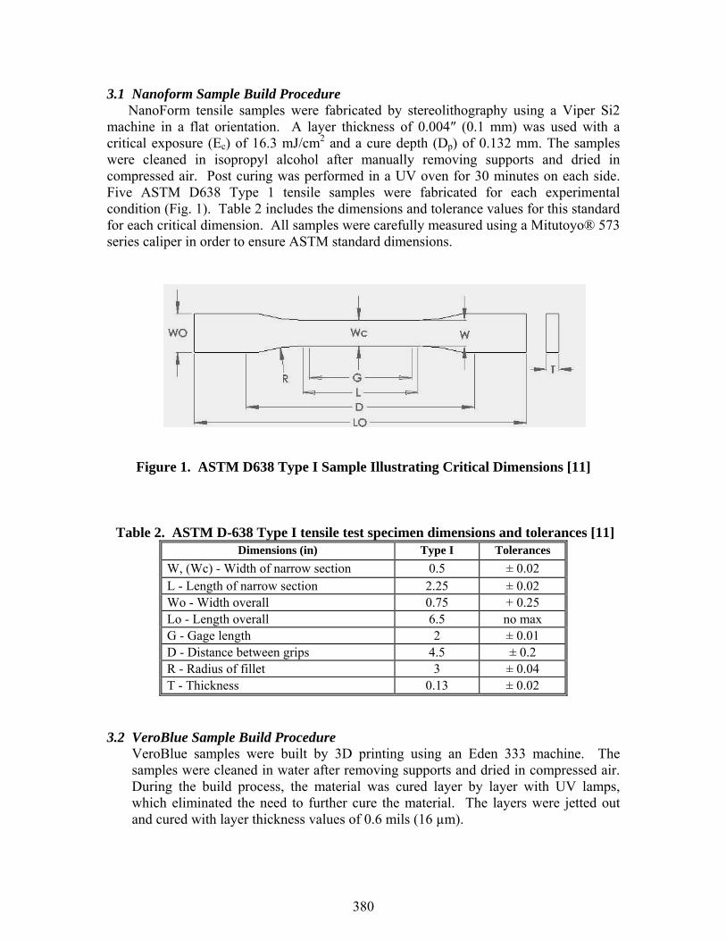
3.1 Nanoform Sample Build Procedure NanoForm tensile samples were fabricated by stereolithography using a Viper Si2 machine in a flat orientation. A layer thickness of 0.004″ (0.1 mm) was used with a critical exposure (Ec) of 16.3 mJ/cm2 and a cure depth (Dp) of 0.132 mm. The samples were cleaned in isopropyl alcohol after manually removing supports and dried in compressed air. Post curing was performed in a UV oven for 30 minutes on each side. Five ASTM D638 Type 1 tensile samples were fabricated for each experimental condition (Fig. 1). Table 2 includes the dimensions and tolerance values for this standard for each critical dimension. All samples were carefully measured using a Mitutoyo® 573 series caliper in order to ensure ASTM standard dimensions.
Figure 1. ASTM D638 Type I Sample Illustrating Critical Dimensions [11] Table 2. ASTM D-638 Type I tensile test specimen dimensions and tolerances [11]
Dimensions (in) Type I Tolerances W, (Wc) - Width of narrow section 0.5 ± 0.02 L - Length of narrow section 2.25 ± 0.02 Wo - Width overall 0.75 + 0.25 Lo - Length overall 6.5 no max G - Gage length 2 ± 0.01 D - Distance between grips 4.5 ± 0.2 R - Radius of fillet 3 ± 0.04 T - Thickness 0.13 ± 0.02
3.2 VeroBlue Sample Build Procedure
VeroBlue samples were built by 3D printing using an Eden 333 machine. The samples were cleaned in water after removing supports and dried in compressed air. During the build process, the material was cured layer by layer with UV lamps, which eliminated the need to further cure the material. The layers were jetted out and cured with layer thickness values of 0.6 mils (16 µm).
380

3.3 Electroless Ni Plating Procedure The electroless plating procedure used in this study can be divided into two main
steps, surface preparation and plating. The surface preparation steps include etching, neutralization, sensitization and surface activation.
Etching
Neutralization
Sensitization
Catalytic activation
Electroless nickel plating
The two etchants chosen for this study were chromic acid (CrO3) and potassium permanganate (KMnO4). The chromic acid etchant was a combination of 21 mL/L of concentrated sulfuric acid and chromic acid concentrations of 300, 325, 350 and 375 g/L in deionized water (DI) at a temperature of 60–65oC. The etch times used for the chromic acid etchant were 2, 5 and 10 minutes (Table 1). The potassium permanganate etchant contained 60g/L sodium hydroxide (NaOH) and a concentration series of 40, 50, 60 and 70g/L of potassium permanganate dissolved in DI water at 80–85oC (Table 1). The samples were rinsed two times in DI water after each step in the electroless Ni plating process. The samples were etched and neutralized in order to remove the excess etchant from the substrate surface. The chromic acid etched samples were rinsed in DI water and neutralized in 2% NH4OH for 30 seconds. The samples etched in potassium permanganate were immersed in oxidant sulfuric acid solution (2% vol. H2SO4 and 2% vol. H2O2) for 5 minutes. The samples were then sensitized (pre-activation) with a solution of 80 g/L of stannous chloride (SnCl2) and 45 mL/L of concentrated hydrochloric acid (HCl) dissolved in DI water at room temperature. The sensitized substrate surface was activated with palladium catalyst at room temperature. The catalyst solution contained 1 g/L of palladium chloride (PdCl2), 45 mL/L of concentrated hydrochloric acid and deionized water. The electroless Ni plating bath consisted of 30 g/L of nickel chloride (NiCl2. 6H2O), 10 g/L sodium glycolate (HOCH2CO2Na) and 10 g/L sodium hypophosphite (NaH2PO2. H2O). The catalytically activated samples were transferred carefully to the electroless Ni plating bath maintained at a temperature of 80–85oC with oxygen circulation. The constant temperature of the plating bath was maintained in a circulating water bath. The oxygen circulation in the bath was used to avoid the possibility of spontaneous decomposition of the hypophosphite bath at this temperature. The samples were plated for approximately 5 minutes and removed from the plating bath and cooled to room temperature and cleaned in DI water.
381

3.4 Mechanical Testing of NanoForm and VeroBlue Mechanical testing was carried out using an Instron 5866 tensile testing machine.
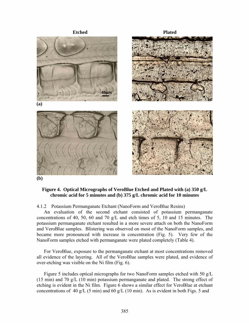
Tensile testing of the NanoForm and VeroBlue samples (ASTM D638, Type 1) were conducted before and after etching. A set of 5 tensile specimens were tested for NanoForm and VeroBlue for each of the design parameters listed in Table 1. The tensile samples were neutralized and rinsed prior to mechanical testing. A comparison was made between the two materials based on etchant type, concentration and etch time. 4. Results and Discussion 4.1 Etching and Plating of NanoForm and VeroBlue Figure 2(a) and (b) are optical micrographs illustrating the surface view of NanoForm and VeroBlue prior to etching. There are distinct differences between the two materials, NanoForm is relatively smooth, while VeroBlue includes obvious layers as a result of the 3D print build process. The exposure of these resins to the chromic acid and potassium permanganate etchants altered the surfaces in a distinct manner that can be attributed to the type of etchant. Plating was successful for most of the samples etched with chromic acid, while the success with the potassium permanganate etchant was sporadic as indicated in Tables 3 and 4. In all cases where plating occurred, the electroless Ni film took on the surface features of the substrate.
(a) (b) Figure 2. Optical view of (a) NanoForm and (b) VeroBlue Samples Prior to
Etching
4.1.1 Chromic Acid Etchant (NanoForm and VeroBlue Resins) The NanoForm and VeroBlue samples were etched with chromic acid at concentrations of 300, 325, 350 and 375 g/L for 2, 5 and 10 minutes at each concentration. For the NanoForm samples, the chromic acid etchant resulted in a fine dispersion of uniform etch pits for most etchant concentrations for etch times less than 10 minutes. For all values of etchant concentrations, surface cracking was observed at etch times of 10 minutes, with some cracking visible at 5 minutes for the highest
45µm
382
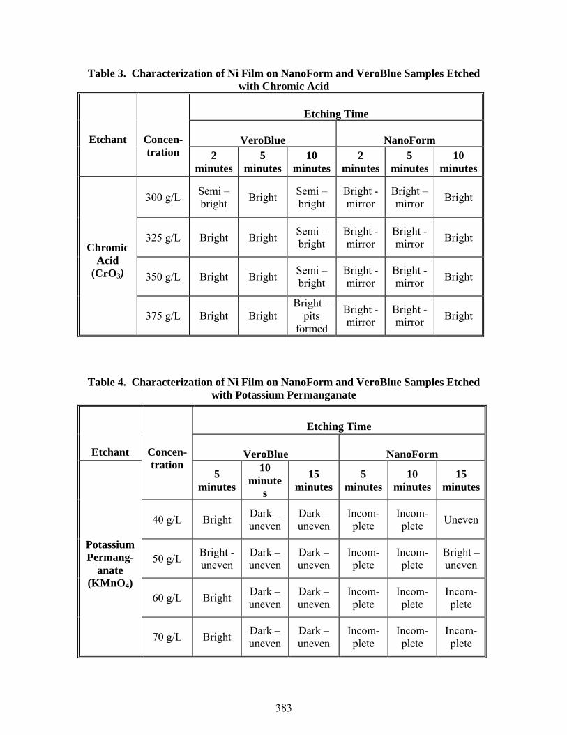
Table 3. Characterization of Ni Film on NanoForm and VeroBlue Samples Etched with Chromic Acid
Etching Time
VeroBlue
NanoForm
Etchant
Concen-tration 2
minutes5
minutes10
minutes2
minutes5
minutes 10
minutes
300 g/L
Semi – bright Bright Semi –
bright Bright - mirror
Bright – mirror Bright
325 g/L
Bright Bright Semi –
bright Bright - mirror
Bright - mirror Bright
350 g/L
Bright Bright Semi –
bright Bright - mirror
Bright - mirror Bright
Chromic Acid
(CrO3)
375 g/L
Bright Bright
Bright – pits
formed
Bright - mirror
Bright - mirror Bright
Table 4. Characterization of Ni Film on NanoForm and VeroBlue Samples Etched with Potassium Permanganate
Etching Time
Etchant
VeroBlue
NanoForm
Concen-tration
5 minutes
10 minute
s
15 minutes
5 minutes
10 minutes
15 minutes
40 g/L
Bright Dark –
uneven Dark – uneven
Incom-plete
Incom-plete Uneven
50 g/L
Bright - uneven
Dark – uneven
Dark – uneven
Incom-plete
Incom-plete
Bright – uneven
60 g/L
Bright Dark –
uneven Dark – uneven
Incom-plete
Incom-plete
Incom-plete
Potassium Permang-
anate (KMnO4)
70 g/L
Bright Dark –
uneven Dark – uneven
Incom-plete
Incom-plete
Incom-plete
383
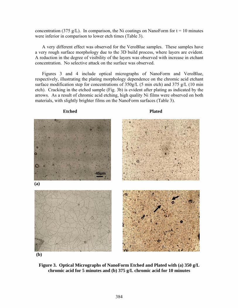
concentration (375 g/L). In comparison, the Ni coatings on NanoForm for t = 10 minutes were inferior in comparison to lower etch times (Table 3). A very different effect was observed for the VeroBlue samples. These samples have a very rough surface morphology due to the 3D build process, where layers are evident. A reduction in the degree of visibility of the layers was observed with increase in etchant concentration. No selective attack on the surface was observed. Figures 3 and 4 include optical micrographs of NanoForm and VeroBlue, respectively, illustrating the plating morphology dependence on the chromic acid etchant surface modification step for concentrations of 350g/L (5 min etch) and 375 g/L (10 min etch). Cracking in the etched sample (Fig. 3b) is evident after plating as indicated by the arrows. As a result of chromic acid etching, high quality Ni films were observed on both materials, with slightly brighter films on the NanoForm surfaces (Table 3).
Etched Plated
(b)
Figure 3. Optical Micrographs of NanoForm Etched and Plated with (a) 350 g/L chromic acid for 5 minutes and (b) 375 g/L chromic acid for 10 minutes
(a)
45µm
384
Etched Plated
(b)
Figure 4. Optical Micrographs of VeroBlue Etched and Plated with (a) 350 g/L chromic acid for 5 minutes and (b) 375 g/L chromic acid for 10 minutes
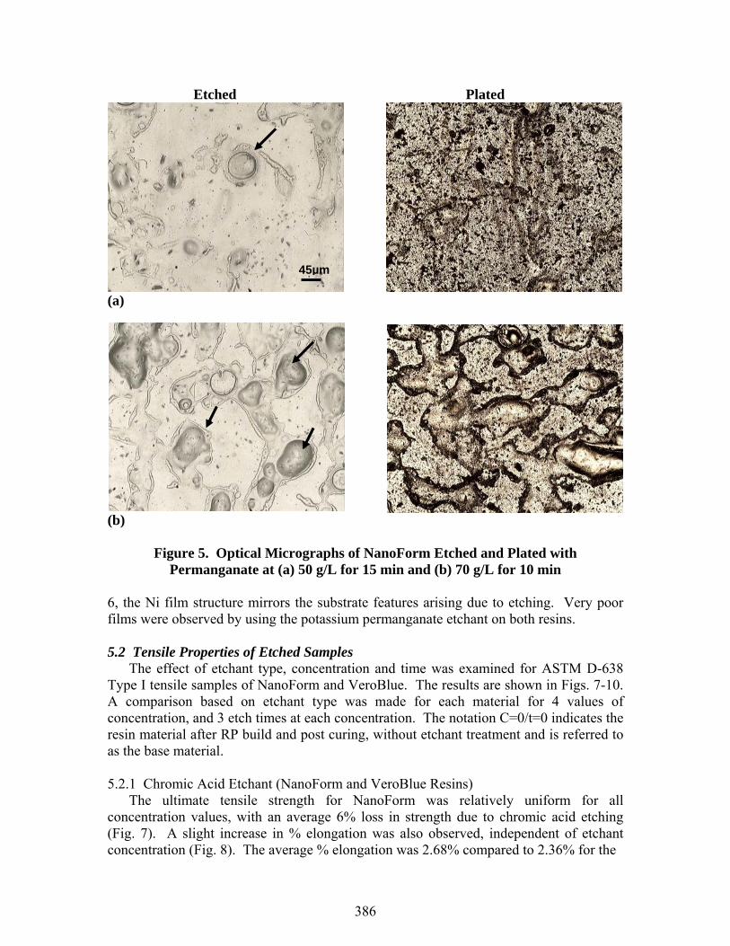
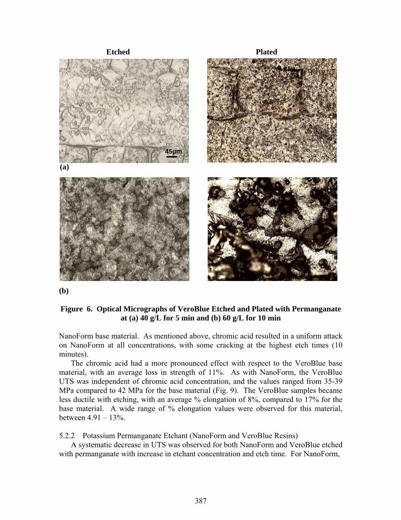
4.1.2 Potassium Permanganate Etchant (NanoForm and VeroBlue Resins) An evaluation of the second etchant consisted of potassium permanganate concentrations of 40, 50, 60 and 70 g/L and etch times of 5, 10 and 15 minutes. The potassium permanganate etchant resulted in a more severe attach on both the NanoForm and VeroBlue samples. Blistering was observed on most of the NanoForm samples, and became more pronounced with increase in concentration (Fig. 5). Very few of the NanoForm samples etched with permanganate were plated completely (Table 4). For VeroBlue, exposure to the permanganate etchant at most concentrations removed all evidence of the layering. All of the VeroBlue samples were plated, and evidence of over-etching was visible on the Ni film (Fig. 6). Figure 5 includes optical micrographs for two NanoForm samples etched with 50 g/L (15 min) and 70 g/L (10 min) potassium permanganate and plated. The strong effect of etching is evident in the Ni film. Figure 6 shows a similar effect for VeroBlue at etchant concentrations of 40 g/L (5 min) and 60 g/L (10 min). As is evident in both Figs. 5 and
(a)
45µm
385
Etched Plated
(a)
(b)
Figure 5. Optical Micrographs of NanoForm Etched and Plated with Permanganate at (a) 50 g/L for 15 min and (b) 70 g/L for 10 min
6, the Ni film structure mirrors the substrate features arising due to etching. Very poor films were observed by using the potassium permanganate etchant on both resins.
5.2 Tensile Properties of Etched Samples The effect of etchant type, concentration and time was examined for ASTM D-638 Type I tensile samples of NanoForm and VeroBlue. The results are shown in Figs. 7-10. A comparison based on etchant type was made for each material for 4 values of concentration, and 3 etch times at each concentration. The notation C=0/t=0 indicates the resin material after RP build and post curing, without etchant treatment and is referred to as the base material. 5.2.1 Chromic Acid Etchant (NanoForm and VeroBlue Resins) The ultimate tensile strength for NanoForm was relatively uniform for all concentration values, with an average 6% loss in strength due to chromic acid etching (Fig. 7). A slight increase in % elongation was also observed, independent of etchant concentration (Fig. 8). The average % elongation was 2.68% compared to 2.36% for the
45µm
386
Etched Plated
(b) Figure 6. Optical Micrographs of VeroBlue Etched and Plated with Permanganate
at (a) 40 g/L for 5 min and (b) 60 g/L for 10 min
NanoForm base material. As mentioned above, chromic acid resulted in a uniform attack on NanoForm at all concentrations, with some cracking at the highest etch times (10 minutes). The chromic acid had a more pronounced effect with respect to the VeroBlue base material, with an average loss in strength of 11%. As with NanoForm, the VeroBlue UTS was independent of chromic acid concentration, and the values ranged from 35-39 MPa compared to 42 MPa for the base material (Fig. 9). The VeroBlue samples became less ductile with etching, with an average % elongation of 8%, compared to 17% for the base material. A wide range of % elongation values were observed for this material, between 4.91 – 13%. 5.2.2 Potassium Permanganate Etchant (NanoForm and VeroBlue Resins) A systematic decrease in UTS was observed for both NanoForm and VeroBlue etched with permanganate with increase in etchant concentration and etch time. For NanoForm,
(a)
45µm
387
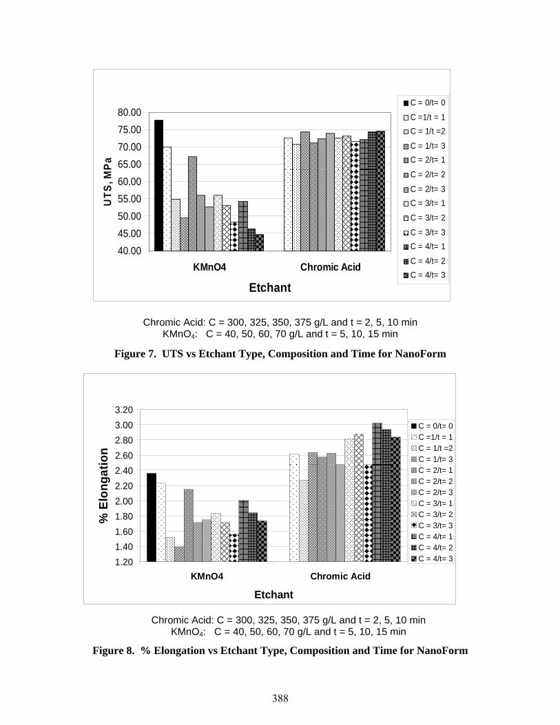
Figure 7. UTS vs Etchant Type, Composition and Time for NanoForm
Figure 8. % Elongation vs Etchant Type, Composition and Time for NanoForm
Chromic Acid: C = 300, 325, 350, 375 g/L and t = 2, 5, 10 min KMnO4: C = 40, 50, 60, 70 g/L and t = 5, 10, 15 min
40.0045.0050.0055.0060.0065.0070.0075.0080.00
KMnO4 Chromic Acid
Etchant
UTS
, MPa
C = 0/t= 0
C =1/t = 1C = 1/t =2
C = 1/t= 3C = 2/t= 1
C = 2/t= 2
C = 2/t= 3C = 3/t= 1
C = 3/t= 2
C = 3/t= 3C = 4/t= 1
C = 4/t= 2C = 4/t= 3
1.201.401.601.802.002.202.402.602.803.003.20
KMnO4 Chromic Acid
Etchant
% E
long
atio
n
C = 0/t= 0C =1/t = 1C = 1/t =2C = 1/t= 3C = 2/t= 1C = 2/t= 2C = 2/t= 3C = 3/t= 1C = 3/t= 2C = 3/t= 3C = 4/t= 1C = 4/t= 2C = 4/t= 3
Chromic Acid: C = 300, 325, 350, 375 g/L and t = 2, 5, 10 min KMnO4: C = 40, 50, 60, 70 g/L and t = 5, 10, 15 min
388
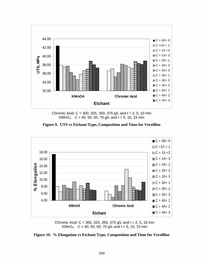
Figure 9. UTS vs Etchant Type, Composition and Time for VeroBlue
Figure 10. % Elongation vs Etchant Type, Composition and Time for VeroBlue
Chromic Acid: C = 300, 325, 350, 375 g/L and t = 2, 5, 10 min KMnO4: C = 40, 50, 60, 70 g/L and t = 5, 10, 15 min
32.00
34.00
36.00
38.00
40.00
42.00
44.00
KMnO4 Chromic Acid
Etchant
UTS
, MPa
C = 0/t= 0C =1/t = 1C = 1/t =2C = 1/t= 3C = 2/t= 1C = 2/t= 2C = 2/t= 3C = 3/t= 1C = 3/t= 2C = 3/t= 3C = 4/t= 1C = 4/t= 2C = 4/t= 3
4.00
6.00
8.00
10.00
12.00
14.00
16.00
18.00
KMnO4 Chromic Acid
Etchant
% E
long
atio
n
C = 0/t= 0C =1/t = 1C = 1/t =2C = 1/t= 3C = 2/t= 1C = 2/t= 2C = 2/t= 3
C = 3/t= 1C = 3/t= 2C = 3/t= 3C = 4/t= 1C = 4/t= 2C = 4/t= 3
Chromic Acid: C = 300, 325, 350, 375 g/L and t = 2, 5, 10 min KMnO4: C = 40, 50, 60, 70 g/L and t = 5, 10, 15 min
389
the UTS decreased from 70 to 45 MPa with increase in etchant concentration, compared to 78 MPa for the base material (Fig. 7). This resulted in an average decrease in strength of 30%. The UTS for VeroBlue ranged from 35-39 MPa, compared to 42 MPa for the base material (Fig. 9). The % elongation decreased significantly for both materials and ranged between 1.39-2.15% for NanoForm, and between 6.53-9.48% for VeroBlue, compared to 2.36 and 17.46%, respectively, for the base materials. This is not surprising, since at most concentrations and etch times, the potassium permanganate etchant resulted in blistering of NanoForm and severe chemical attack on VeroBlue. 5. Conclusions This work explored the effect of the etching process on the mechanical properties of NanoForm and VeroBlue. Chromic acid and potassium permanganate were investigated at various concentrations and etch times as part of an electroless Ni process. The following bulleted list summarizes the important conclusions from this work.
• The chromic acid etchant resulted in a more uniform alteration of the surface for both NanoForm and VeroBlue compared to the potassium permanganate etchant; severe surface damage was observed with the potassium permanganate. The chromic acid etchant created uniform etch pits throughout the surface at most concentrations.
• Surface cracks were observed for etch times of 10 minutes for all chromic acid
concentrations on the NanoForm material. These cracks should be avoided in order to produce high quality films.
• Blistering of the NanoForm samples was observed for most concentrations of the
potassium permanganate etchant. • The chromic acid and potassium permanganate etchants resulted in a decrease in
UTS for all concentrations and etch times for both NanoForm and VeroBlue.
• The degree of surface damage caused by the potassium permanganate etchant was severe on both NanoForm and VeroBlue, with an average decrease in UTS of 30% for NanoForm and 10% for VeroBlue. The % elongation decreased significantly for VeroBlue compared to the non-etched material.
• A smooth surface with fine surface modification throughout will result in the best
electroless Ni coatings with a minimum effect on mechanical properties.
• The surface preparation for NanoForm consisting of chromic acid resulted in the highest quality Ni films for all concentration values.
390
Acknowledgements The facilities within the W.M. Keck Center for 3D Innovation (Keck Center) used here contain equipment purchased through Grant Number 11804 from the W.M. Keck Foundation, a faculty STARS Award from the University of Texas System, and two equipment grants from Sandia National Laboratories. This material is based in part upon work supported through the Mr. and Mrs. MacIntosh Murchison Chair I in Engineering, research contract 504004 from Sandia National Laboratories in the Laboratory Directed Research and Development (LDRD) program, and the National Science Foundation under Grant No. 0245071. The authors are grateful for the assistance of Mahesh Tonde, Karina Puebla, Luis Ochoa, Jesus Flores, Marjorie Ingle and Donovan Barroso within the Keck Center during performance of various aspects of the research. Sandia National Laboratories is a multi-program laboratory operated by Sandia Corporation, a Lockheed Martin Company, for the United States Department of Energy’s National Nuclear Security Administration under contract DE-AC04-94AL85000. References [1] R. Hague, S. Mansour, N. Saleh, R. Harris (2004) “Materials Analysis of Stereolithography Resins for Use in Rapid Manufacturing”, Journal of Materials Science, V39, 2457-2464. [2] N. Saleh, N. Hopkinson, R.J.M. Hague, S. Wise (2004) “Effects of Electroplating on the Mechanical Properties of Stereolithography and Laser Sintered Parts”, Rapid Prototyping Journal, V10, 305-315. [3] A. Pique, S.A. Mathews, B. Pratap, R.C.Y. Auyeung, B.J. Karns, S. Lakeou (2006) “Embedded Electronic Circuits by Laser Direct-Write”, Microelectronic Engineering, V83, 2527-2533. [4] K.S. Chen, J.L. Zich, W.P. Morgan (1997) “Low-Cost Pd Catalyzed Metallization Technology for Rapid Prototyping of Electronic Substrates and Devices”, 1997 Laboratory Directed Research and Development Annual Report, 116-117. [5] Y. Shacham-Diamond, S. Lopatin (1999) “Integrated Electroless Metallization for ULSI”, Electrochimica Acta, 3639-3649. [6] A. Lopes, M. Navarette, F. Medina, J.A. Palmer, E. MacDonald, R.B. Wicker (2006) “Expanding Rapid Prototyping for Electronic Systems Integration of Arbitrary Form”, 17th Annual Solid Freeform Fabrication Symposium, The University of Texas at Austin, August 14-16, Austin, TX. [7] M. Navarrete, A. Lopes, J. Acuna, R. Estrada, E. MacDonald, J. Palmer, R. Wicker (2007) “Integrated Layered Manufacturing of a Novel Wireless Motion Sensor System with GPS”, The Eighteenth Solid Freeform Fabrication Proceedings, The University of Texas at Austin, August 6-8, Austin, TX. to appear. [8] J.E. McCaskie (2005) “A Survey of Mechanisms of Adhesion of Metal Films to Plastic Surfaces”, AIFM Galvano Tecnica e Nuove Finiture, V15-16, 210-219. [9] R.C Agarwala and V. Agarwala (2003) “Electroless alloy/composite coatings: A review”, Sadhana, Indian Academy of Sciences V28, 475– 493. [10] Glenn.O.Mallory and Juan B.Hajdu (1990) “Electroless Plating Fundamentals and Applications”, American Electroplaters and Surface Finishers Society, Orlando, FA. [11] American Society of Testing and Materials Standard 638 (2005) “Standard Test Method for Tensile Properties of Plastics”, Annual Book of ASTM Standards, West Conshohocken, PA.
391