effect of package trace and termination resistance on tx
TRANSCRIPT

IEEE P802.3cd 50/100/200GbE Task Force
Effect of Package Trace and
Termination Resistance
on Tx Specification
Yasuo Hidaka
Fujitsu Laboratories of America, Inc.
IEEE P802.3cd Task Force
Ad hoc Teleconference, October 26, 2016

Background
I have reported that we may need to revise package trace impedance (Zc, 90Ω) and termination resistance (Rd, 55Ω) in the COM parameters, because they do not necessarily cover corner cases (hidaka_100516_3cd_adhoc.pdf)
There was a concern that Tx-related COM parameters such as signal amplitude and SNRTX may have to be changed consistently with package parameters, because Tx output amplitude and Tx SNDR will be also affected by the package trace impedance and termination resistance
Hence, I have studied the effect of package trace impedance and termination resistance on Tx output amplitude and Tx SNDR
1 IEEE P802.3cd 50/100/200GbE Task Force

Simulated Package Parameters
The following 10 combinations of parameters were simulated
The original conditions were #3 and #7
The proposed conditions were #2/#3/#4 and #6/#7/#8
See hidaka_100516_3cd_adhoc.pdf 2 IEEE P802.3cd 50/100/200GbE Task Force
Case zp
Package trace length
Rd
Termination resistance
Zc
Package trace impedance
#1
12 mm
45 Ω 90 Ω
#2 110 Ω
#3 55 Ω
90 Ω
#4 110 Ω
#5
30 mm
45 Ω 90 Ω
#6 110 Ω
#7 55 Ω
90 Ω
#8 110 Ω
#9 12 mm 50 Ω 100 Ω
#10 30 mm

Simulated Model
Tx filter: 𝑆21 = EQ93A−46 𝑇𝑟 = 13ps, 𝛽 = 2 (i.e. 13ps 20-80% Tr)
Device terminator: S21 = 1, 𝑆22 =𝑅𝑑−50Ω
𝑅𝑑+50Ω (i.e. same as Tx in COM)
No effect of impedance matching on amplitude (i.e. only effect on reflection)
Device capacitor: 𝑆 = EQ93A−8 𝐶 = 𝐶𝑑
Package trace: 𝑆 = EQ93A−13,14 Table93A−3 except 𝑍𝑐 , 𝑧𝑝
Package capacitor: 𝑆 = EQ93A−8 𝐶 = 𝐶𝑝
Test fixture: 𝑆21 = 10− EQ93−1 /20, ∠𝑆21 = minimum phase 𝑆21
Scope terminator: 𝑆21 = 1, 𝑆11 = 0 (i.e. ideal)
Scope filter: 4-th order Bessel-Thomson LPF with 33GHz 3dB BW
𝜔0 = 98.28967142447435 G rad/s 3 IEEE P802.3cd 50/100/200GbE Task Force
Tx
filter
Rd
Device
termi-
nator
Device
capacitor
Package
trace
Package
capacitor
Test
fixture
Scope
termi-
nator
Scope
filter
Cd Zc, zp Cp
TP0 TP0a
ILref Ideal 13ps Tr 33GHz BT

0.900.910.920.930.940.950.960.970.980.991.001.011.021.031.04
-1.0 -0.8 -0.6 -0.4 -0.2 0.0 +0.2 +0.4 +0.6 +0.8 +1.0 AVG
v f
Gain expansion / compression (dB)
vf (zp=30mm, Np=200)
#5 Rd=45 Zc=90 #6 Rd=45 Zc=110 #7 Rd=55 Zc=90
#8 Rd=55 Zc=110 #10 Rd=50 Zc=100
0.94
0.95
0.96
0.97
0.98
0.99
1.00
1.01
1.02
1.03
1.04
-1.0 -0.8 -0.6 -0.4 -0.2 0.0 +0.2 +0.4 +0.6 +0.8 +1.0 AVG
v f
Gain expansion / compression (dB)
vf (zp=12mm, Np=200)
#1 Rd=45 Zc=90 #2 Rd=45 Zc=110 #3 Rd=55 Zc=90
#4 Rd=55 Zc=110 #9 Rd=50 Zc=100
Effect on vf (Np=200)
The effect of Rd and Zc on vf is very small
4 IEEE P802.3cd 50/100/200GbE Task Force

0.68
0.69
0.70
0.71
0.72
0.73
0.74
0.75
0.76
0.77
0.78
-1.0 -0.8 -0.6 -0.4 -0.2 0.0 +0.2 +0.4 +0.6 +0.8 +1.0 AVG
pm
ax
Gain expansion / compression (dB)
pmax (zp=30mm, Np=200)
#5 Rd=45 Zc=90 #6 Rd=45 Zc=110 #7 Rd=55 Zc=90
#8 Rd=55 Zc=110 #10 Rd=50 Zc=100
0.74
0.75
0.76
0.77
0.78
0.79
0.80
0.81
0.82
0.83
0.84
-1.0 -0.8 -0.6 -0.4 -0.2 0.0 +0.2 +0.4 +0.6 +0.8 +1.0 AVG
pm
ax
Gain expansion / compression (dB)
pmax (zp=12mm, Np=200)
#1 Rd=45 Zc=90 #2 Rd=45 Zc=110 #3 Rd=55 Zc=90
#4 Rd=55 Zc=110 #9 Rd=50 Zc=100
Effect on pmax (Np=200)
The effect of Rd and Zc on pmax is very small
5 IEEE P802.3cd 50/100/200GbE Task Force

0.720
0.725
0.730
0.735
0.740
0.745
0.750
-1.0 -0.8 -0.6 -0.4 -0.2 0.0 +0.2 +0.4 +0.6 +0.8 +1.0 AVG
pm
ax/
v f
Gain expansion / compression (dB)
pmax / vf (zp=30mm, Np=200)
#5 Rd=45 Zc=90 #6 Rd=45 Zc=110 #7 Rd=55 Zc=90
#8 Rd=55 Zc=110 #10 Rd=50 Zc=100
0.790
0.795
0.800
0.805
0.810
0.815
0.820
-1.0 -0.8 -0.6 -0.4 -0.2 0.0 +0.2 +0.4 +0.6 +0.8 +1.0 AVG
pm
ax/
v f
Gain expansion / compression (dB)
pmax / vf (zp=12mm, Np=200)
#1 Rd=45 Zc=90 #2 Rd=45 Zc=110 #3 Rd=55 Zc=90
#4 Rd=55 Zc=110 #9 Rd=50 Zc=100
Effect on the Ratio of pmax to vf (Np=200)
The effect of Rd and Zc on the ratio of pmax to vf is rather small between proposed conditions (#2/3/4, #6/7/8)
6 IEEE P802.3cd 50/100/200GbE Task Force

30
35
40
45
50
55
-1.0 -0.8 -0.6 -0.4 -0.2 0.0 +0.2 +0.4 +0.6 +0.8 +1.0 AVG
SND
R (
dB
)
Gain expansion / compression (dB)
SNDR (zp=30mm, Np=200)
#5 Rd=45 Zc=90 #6 Rd=45 Zc=110 #7 Rd=55 Zc=90
#8 Rd=55 Zc=110 #10 Rd=50 Zc=100
30
35
40
45
50
55
-1.0 -0.8 -0.6 -0.4 -0.2 0.0 +0.2 +0.4 +0.6 +0.8 +1.0 AVG
SND
R (
dB
)
Gain expansion / compression (dB)
SNDR (zp=12mm, Np=200)
#1 Rd=45 Zc=90 #2 Rd=45 Zc=110 #3 Rd=55 Zc=90
#4 Rd=55 Zc=110 #9 Rd=50 Zc=100
Effect on SNDR (Np=200)
The effect of Rd and Zc on SNDR is very small
7 IEEE P802.3cd 50/100/200GbE Task Force
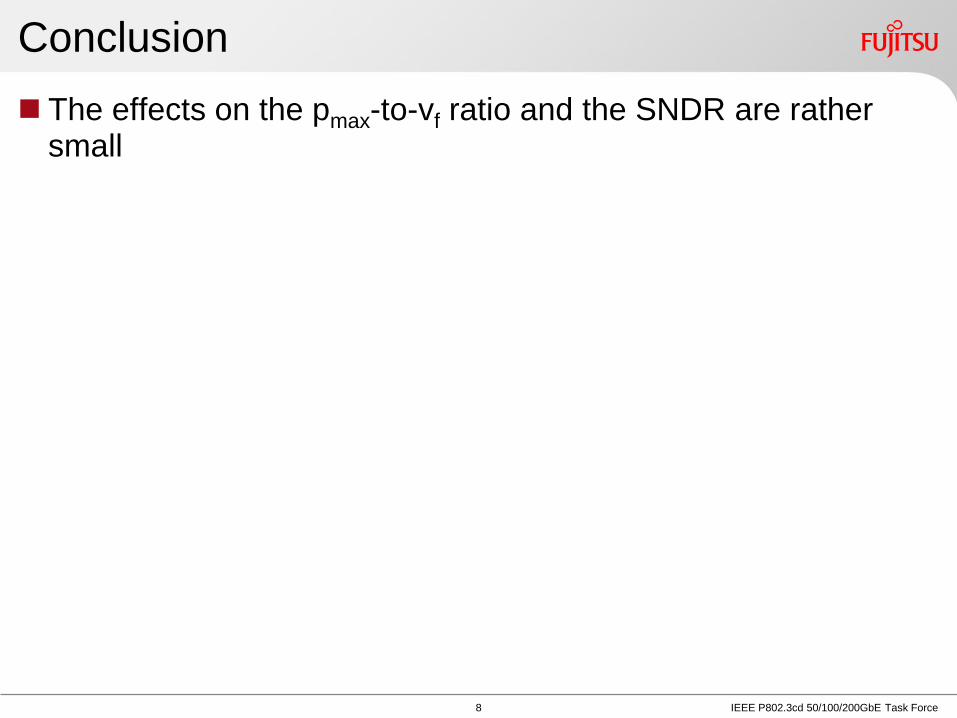
Conclusion
The effects on the pmax-to-vf ratio and the SNDR are rather small
8 IEEE P802.3cd 50/100/200GbE Task Force

IEEE P802.3cd 50/100/200GbE Task Force
Back up Slides
Simulation Methodology
9

Simulation Methodology
1. Get 𝑆21 of the entire model from 1MHz to 𝑓𝑚𝑎𝑥 with 1MHz step
𝑓𝑚𝑎𝑥 = 26.5625GHz ×𝑀 ÷ 2, where 𝑀 = 32
2. Get a single-bit pulse response
3. Get a linear cycle response of PRBS13Q with ideal levels
4. Cancel the DC offset of the linear cycle response of PRBS13Q
5. Get a non-linear cycle response of PRBS13Q by gain expansion / compression (similar to a methodology in healey_3bs_02_0916)
Simulated from -1.0dB to +1.0dB with 0.2dB step
6. Get V0, V1, V2, and V3 per 120D.3.1.2.1
7. Get Vmid, ES1, and ES2 per 120D.3.1.2
8. Get ES=(ES1+ES2)/2 per 120D.3.1.3
9. Get linear fit pulse p(k) and error e(k) per 120D.3.1.3, 94.3.12.5.2, 85.8.3.3.5
Dp=2 and Np=200
10. Get steady-state voltage vf and linear fit pulse peak pmax per 120D.3.1.4
11. Get 𝜎𝑒 from e(k), then get SNDR per 120D.3.1.6
𝜎𝑛 is always set to 𝑝𝑚𝑎𝑥 × 10 −50 20 (i.e. -50dB) to have noise floor 10 IEEE P802.3cd 50/100/200GbE Task Force
From healey_3bs_02_0916

IEEE P802.3cd 50/100/200GbE Task Force
Thank you
11