effect of geometry on void formation in commercial ...ccc.illinois.edu/s/reports08/okelman_m...
TRANSCRIPT

Author's personal copy
Effect of geometry on void formation in commercial electroplatingof thin strips to copper
M.K. Okelman, B.G. Thomas ⁎, M. Powers 1
Department of Mechanical Science and Engineering, University of Illinois: Urbana-Champaign, Urbana, IL 61801, United States
Received 15 October 2007; accepted in revised form 3 March 2008Available online 14 March 2008
Abstract
Three plating trials comprised of six samples were performed to evaluate the ability to attach thin strips of varying cross section to a coppersubstrate via commercial nickel electroplating in a nickel sulfamate bath. Nickel plated to the top, bottom, and sides of the nickel strips, as well asto the substrate. A significant void formed beneath rectangular nickel strips for all geometries studied, including strip widths of 500 µm to5000 µm and gap thicknesses from 100 µm to 1500 µm. This is due to the starvation of ions when two regions of growing grains impinge andentrap a volume of electrolyte, surrounding it completely by deposited nickel. Impingement often occurs just past the edge of the strip whichcauses the void width to be greater than the strip width and form seams at the edge of the void. The rate of plating is greatest in areas where sharpcorners exist, due to higher current density. More plating reaches under the strip as the width decreases and/or gap thickness increases. Thus, thevoid size decreases with decreasing aspect ratio, defined as the strip width over gap thickness. The use of a cylindrical strip produces sound platingwith no voids. This is because the lack of corners allows impingement to occur first beneath the center of the circular cross section, so liquid isnever surrounded. The results of this study demonstrate how to minimize or avoid void formation in commercial electroplating of suspended stripswhich is of great importance in the installation of sensor strips in the coating layer of continuous casting molds.© 2008 Elsevier B.V. All rights reserved.
Keywords: Electroplating; Defects; Voids; Metal embedding; Coating failure; Thin film microsensors
1. Introduction
Electroplating is one method to attach a thin strip to a metalsubstrate by embedding it into the coating layer. Other methodsto attach dissimilar metals include diffusion bonding [1–4],ultrasonic welding [5–7], and metallic paste [8,9]. Diffusionbonding requires some solid solubility between the two metalsto be joined, such as that between copper and nickel. The twometals must also survive the necessary temperature and pressureassociated with the hot isostatic pressing (HIP) process. Ultra-sonic welding is suitable for welding materials of differentthicknesses, such as thin foils to thick substrates, and is lesssensitive to surface contamination.
The electroplating method has the advantage of simplicityand low cost [10]. It also embeds the strip within the coatinglayer, which affords protection and a smooth exposed surface(after machining). This is very beneficial when the strip containsdelicate sensors, or when the surface of the substrate and stripmust be flat [11,12]. However, when electroplating over com-plex geometries, defects such as voids or seams often appear, dueto different rates of deposition throughout the geometry [13,14].Such voids can be catastrophic, leading to spalling of the coatinglayer, if it is subjected to sudden temperature changes [15,16]Previous electroplating studies include measurements of me-chanical properties [17,18] and models of the process [19–21].Films of different surface morphology, thickness uniformity,grain size, and properties can be achieved by adjusting thecurrent density, deposition technique, and/or composition of thesolution bath [17]. Mathematical models of electroplating focuson the macro and micro-scale, including analytical models[19] as well as numerical models [20,21] which are compared to
Available online at www.sciencedirect.com
Surface & Coatings Technology 202 (2008) 4153–4158www.elsevier.com/locate/surfcoat
⁎ Corresponding author.E-mail address: [email protected] (B.G. Thomas).
1 Siemens VAI Services, LLC – Benton Harbor, MI, Benton Harbor, MI49022.
0257-8972/$ - see front matter © 2008 Elsevier B.V. All rights reserved.doi:10.1016/j.surfcoat.2008.03.004

Author's personal copy
experimental data. None of this previous work has quantified theeffect of strip geometry on the formation of voids or seamsduring electroplating.
This work investigates the attachment of strips to a substrateby affixing the suspended strip above the substrate and electro-plating in a commercial facility. Three plating trials comprisedof six samples were performed to quantify the effect of stripwidth, gap thickness, strip geometry (rectangular versus cir-cular), and strip conductivity (non-conductive versus conduc-tive) on the ability to attach thin strips to a copper substrate.
2. Electroplating process
Commercial electroplating involves depositing a metalcoating layer onto a metal substrate via electrolysis. The elec-troplating process requires an electric circuit be completedthrough the bath, which includes electrons flowing to the cath-ode (substrate) from the anode (source metal), as well as re-turning through a conducting electrolyte containing the metalions, driven by a DC power source. For the nickel sulfamateplating bath used in this work, the reactions are:
Cathode: Ni2þ þ 2e−YNi;
Anode: NiY 2e−þ Ni2þ
Metal ions arrive at the cathode surface through three prin-ciple paths: electrical migration, diffusion, and convection, bothnatural and forced, which replaces low ion concentration elec-trolyte with high ion concentration electrolyte [22]. Electrolytefluid flow can be well represented by solving the incompres-sible Navier–Stokes equations in the entire bath, including theeffects of thermal buoyancy. An additional time-dependentadvection–diffusion equation is needed for the mass transportof the ions, which are carried by the liquid while diffusingthrough the liquid. The electric field, assumed to be steady-state, can be determined from a Laplace equation knowing theelectric potential and the electrical conductivity. The effects ofion migration can be neglected if there is excess supportingelectrolyte [20], such as the case for a large commercial bath.
It is also sometimes important to include time-dependent filmresistance variation which occurs during the plating growth. Thechanging thickness leads to variations in the ion concentrationand electric field near the cathode surface [20]. The theoreticalplating thickness (assuming 100% current efficiency) can becalculated using Faraday's law [23,24]:
T ¼ ItMzF
1ad
where T is the thickness of the plating (cm), I is the current (A), tis the time (s), M is the atomic weight (58.7 g/mol), z is the ionvalence (2), F is Faraday's constant (96,500), a is the substratearea (cm2), and d is the density of the plating material (8.9 g/cm3).This equation holds both locally (if local values can be found),and on average (based on the total time and plating area).
3. Experimental procedure
Three plating trials comprised of six samples were per-formed. Samples 1 and 3 were placed on one copper substrate,samples 2 and 4 were placed on another copper substrate, andsamples 5 and 6 were placed on separate substrates. Thisarrangement made it possible to simultaneously investigate theeffect of gap thickness and strip width on the ability to attachthin strips to a copper substrate.
In the constant gap thickness trial (samples 1 and 2), a thintriangular strip of rectangular cross section was held a constantdistance above a copper substrate to test how the width of thestrip affects the ability of nickel atoms to plate around the strip(Fig. 1). For sample 1, the strip width ranged from 1623 to4924 µm, while the gap thickness was kept constant at ~589 µm.For sample 2, the strip width ranged from 725 to 2759 µm, whilethe gap thickness was kept constant at ~1647 µm.
In the constant strip width trial (samples 3 and 4), a rectan-gular strip of constant width was attached to the copper sub-strate a varying distance above the copper substrate to test howthe distance between the nickel strip and the copper substrate,(i.e. the gap thickness), affects the plating ability (Fig. 1). Forsample 3, the gap thickness ranged from 96 to 302 µm, whilethe strip width was kept constant at 1825 µm. For sample 4, the
Fig. 1. Illustration of (a) constant gap thickness trial (sample 1) and (b) constant strip width trial (sample 3).
4154 M.K. Okelman et al. / Surface & Coatings Technology 202 (2008) 4153–4158

Author's personal copy
gap thickness ranged from 156 to 1317 µm, while the stripwidth was kept constant at 500 µm. Observed aspect ratios (stripwidth to gap thickness) ranged from 0.35 to 19.0.
The circular strip geometry trial (samples 5 and 6) inves-tigated the effects of cross section shape and strip conductivityby plating over fibers with circular cross section at variousdistances above the substrate. Sample 5 consisted of acylindrical “strip” of non-conducting optical fiber suspended0 to 1524 µm above the substrate. The optical fiber wascomposed of a plastic protective outer coating surrounding acladding layer and glass inner core. With the plastic coating thefiber has a diameter of 200 µm, while the cladding layersurrounding the glass core has a diameter of 125 µm. The glasscore itself is only 9 µm in diameter. Sample 6 consisted of acylindrical tube of 316 stainless steel with an outer diameter of254 µm and inner diameter of 127 µm suspended a constantdistance of about 10 µm above the substrate.
The copper substrate was etched with nitric acid prior to theinstallation of the strips to clean the copper surface beforeelectroplating. The nickel strips were cleaned by scrubbing withcalcium carbonate and a 3-M burgundy Scotch-Brite abrasivepad. As shown in Fig. 2, the strips were then suspended justabove the copper substrate to perform a constant gap thicknesstrial and a constant strip width trial simultaneously. Yellowvinyl tape was attached to the copper substrate to achieve thedesired gap thickness profile between the strips and thesubstrate. An investigation of the effect of electrically insulatingthe suspended strip from the grounded substrate was initiated bypreventing some strips, via tape, from contacting the copper
substrate. Each assembly was then masked prior to elec-troplating. The optical fiber (sample 5) and the stainless steeltube (sample 6) were not treated before plating.
Each assembly was pretreated by rinsing with DI water andimmersing in a 10% sulfamic solution to clean the surfaces. Thestrips did not seem to suffer any negative effects due to this pre-treatment. Each assembly was then placed in a nickel sulfamatebath with a concentration of 1.5 mole/l at a commercial platingfacility in Benton Harbor, Michigan. Due to the high solubilityof the salts of sulfamic acid, high concentrations of nickel ionsare possible, permitting high rates of plating. This same com-mercial facility and procedure is used to plate copper continuouscasting molds for the steel industry. The substrate area was2500mm2; so 0.75 amps of current were required for 0.0254mmof plating per hour. A potential of 1.8 V was applied between thecopper substrate and suspended nickel strips (cathode) and agrated metal basket of nickel pieces that comprised the anodelocated ~150 mm away in the bath. After 65 h a total of 2.08 mmof nickel (ultrasonic measurement) was deposited on the coppersubstrate.
For the constant gap thickness trial and constant strip widthtrial the electroplated nickel strip was cut into cross sectionsusing wire electrical discharge machining (EDM). Each samplewas mounted in epoxy, rough ground with 180 grit SiC paper,hand ground with 240, 320, 400, and 600 grit, and machine
Fig. 3. Close-up of void region where quantitative measurements were made.
Fig. 4. Impingement often occurs just past the edge of the strip which causes thevoid width to be greater than the strip width and form seams at the edge of thevoid (a) sample 1 (b) sample 3.
Fig. 2. Nickel strips mounted to the copper substrate (a) sample 1 (b) sample 3.
4155M.K. Okelman et al. / Surface & Coatings Technology 202 (2008) 4153–4158

Author's personal copy
ground using 800 and 1200 grit. Machine polishing was alsoperformed with a short knap cloth and 1 µm solution and 0.3 µmsolution when necessary to obtain a mirror-like finish. Etchingwas performed by immersing each sample in 1 part nitric acid, 1part acetic acid (glacial), and 1 part DI water for 15 s.
4. Results and discussion
Optical microscopy was used to identify the strip locationand the surrounding plating structure. The void thickness andwidth were measured from traces of the photographs. In addi-tion, the gap thickness and the thickness of the nickel platingunder the strip were measured at 6 different locations: aboveand below the void at left, right, and center (Fig. 3). For bothtrials, a plot of the void thickness, void width, gap thickness,and strip width versus the distance along the copper substratewas created (Fig. 4).
Plating growth impingement often occurs just past the edgeof the strip which causes the void width to be greater than thestrip width and form seams at the edge of the void. Fig. 4 alsoshows that as the strip width decreases, the void thicknessdecreases and more plating occurs under the nickel strip. Basedon this observation, it is proposed that the extent of platingunder the nickel strip is related to the aspect ratio, defined as theratio of the strip width to the gap thickness (Fig. 5). Specifically,more plating reaches under the nickel strip as the aspect ratiodecreases. In the constant gap thickness trial, this is due to thedecrease in strip width, while in the constant strip width trial, thesame observation is due to the increase in gap thickness.
The sequence of events leading to the observed microstruc-ture and void shape is sketched in Fig. 6. Nickel plated onto thecopper substrate and to the top, bottom, and sides of the nickelstrip, even when there was no physical connection to the coppersubstrate. The plating layers on each of the nickel strips grewoutwards at the same rate regardless of whether or not it wasinsulated on its ends. This indicates that the nickel strip iseffectively grounded through the conductive bath across theshort distance to the copper substrate. The theoretical averagedeposit thickness was calculated as 2.40 mm, which is veryclose to the 2.08 mm actually measured. Minor plating thick-ness abnormalities at the edges of the small copper substratewere responsible for the difference. However, the plating
Fig. 6. Early on the plating growing from the corners of the strip contacts theplating originating from the substrate and “starves” the region beneath the stripfrom nickel ions, creating a void.Fig. 5. More plating is obtained underneath the strip as the aspect ratio decreases.
4156 M.K. Okelman et al. / Surface & Coatings Technology 202 (2008) 4153–4158
Author's personal copy
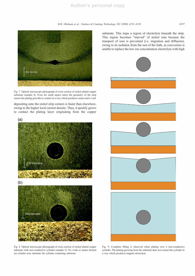
depositing onto the nickel strip corners is faster than elsewhere,owing to the higher local current density. Thus, it quickly growsto contact the plating layer originating from the copper
substrate. This traps a region of electrolyte beneath the strip.This region becomes “starved” of nickel ions because thetransport of ions is prevented (i.e. migration and diffusion),owing to its isolation from the rest of the bath, as convection isunable to replace the low ion concentration electrolyte with high
Fig. 9. Complete filling is observed when plating over a non-conductivecylinder. The plating growing from the substrate does not contact the cylinder ina way which produces trapped electrolyte.
Fig. 8. Optical microscope photograph of cross section of nickel plated coppersubstrate with non-conductive cylinder (sample 5). No voids or seams formed(a) cylinder near substrate (b) cylinder contacting substrate.
Fig. 7. Optical microscope photograph of cross section of nickel plated coppersubstrate (sample 4). Even for small aspect ratios the geometry of the stripcauses the plating growths to contact in a way which produces seams and a void.
4157M.K. Okelman et al. / Surface & Coatings Technology 202 (2008) 4153–4158

Author's personal copy
ion concentration electrolyte. As in shrinkage-cavity macro-porosity observed in metal foundry castings [25–27], a liquidregion completely surrounded by solid will result in a void, asseen in Fig. 7. As a consequence, every rectangular specimencontained a void between the rectangular strip and substrate.Even moving the strip almost three widths away from thesubstrate is not enough to prevent void formation.
When plating over a non-conductive cylinder (sample 5),complete filling is observed, as seen in Figs. 8 and 9. The lack ofa void in this geometry is expected because 1) without corners,the growth rates from the cylinder surface are almost uniform,and 2) the plating growing from the copper substrate has furtherdistance to reach the cylinder extremities. Fig. 8 shows that thenickel grain structure originated from the copper substrate andgrew up and around the non-conductive cylinder. The cylinderremained non-conductive and uncharged so no detectable de-posit formed on its surface. In the case of a conductive cylinderas in sample 6 (not pictured), the plating layer growing from thecylinder is almost uniform, owing to the lack of corners. Thus,the plating from the copper substrate first contacts the cylindernear its center. This avoids entrapping electrolyte and thereforeprevents void formation. Thus, cylindrical fibers experiencesound plating, regardless of their insulating properties.
5. Conclusions
This work investigates the attachment of suspended strips toa copper substrate by electroplating. Three plating trials com-prised of six samples were performed to evaluate the platingability to attach thin strips to a copper substrate by measuringthe occurrence and size of voids found under the strips. As thestrip width decreases, or gap thickness increases, more platingpenetrates under the strip. In other words, the aspect ratioroughly governs the fraction of the gap filled by the plating.Voids form beneath rectangular strips even for aspect ratios lessthan one. The plating growing from the strip corners contactsthe plating originating from the substrate and “starves” theregion beneath the strip from ions. The use of a cylindrical stripproduces sound plating with no voids because the lack ofcorners allows impingement to occur first beneath the center ofthe circular cross section. The results of this study can be used tominimize or avoid void formation in commercial electroplatingof suspended strips which is of great importance in the in-stallation of sensor strips in the coating layer of continuouscasting molds.
Acknowledgments
Funding for this work was provided by the National ScienceFoundation under contract CMMI 05-28668 and the UIUC
Continuous Casting Consortium. Optical microscopy was car-ried out in the Frederick Seitz Materials Research LaboratoryCentral Facilities, University of Illinois, which is partiallysupported by the U.S. Department of Energy under grants DE-FG02-07ER46453 and DE-FG02-07ER46471.
References
[1] I.S. Batra, G.B. Kale, T.K. Saha, A.K. Ray, J. Derose, J. Krishnan, Mater.Sci. Eng. A369 (2002) 119.
[2] L. Esposito, A. Bellosi, S. Guicciardi, G. De Portu, J. Mater. Sci. 33 (1998)1827.
[3] M. Eroglu, T.I. Khan, N. Orhan, Mater. Sci. Technol. 18 (2002).[4] F.M. Coughlan, H.J. Lewis, J. Mater. Process. Technol. 153–154 (2004)
240.[5] J.M. Peterson, H.L. McKaig, C.F. DePrisco, IRE Natl. Conv. (1962) 3.[6] J. Antonevich, IRE Transactions on Ultrasonic Engineering, vol. 71, 1960,
p. 26.[7] S.A. Francis, IEEE Transactions on Product Engineering and Production,
vol. 71, 1963, p. 13.[8] K. Hayashi, A. Ishikawa, T. Endho, H. Yamagishi, IEEE First World
Conference on Photovoltaic Energy Conversion, vol. 1, 1994, p. 535.[9] P.W. Krempl, C. Reiter, W. Wallnofer, J. Neubig, Proceedings of the IEEE
2002 Ultrasonics Symposium, vol. 1, 2002, p. 949.[10] M. Schlesinger, M. Paunovic, Modern Electroplating, 4th ed.Wiley, New
York, NY, 2000.[11] X. Li, F. Prinz, J. Manuf. Sci. Eng. 125 (2003) 1.[12] H. Choi, A. Datta, X. Cheng, X. Li, J. Microelectromechnical Syst. 15 (2)
(2006) 322.[13] J. Jorne, A.M. Tran, Proceedings of the IEEE 2001 International
Interconnect Technology Conference, 2001, p. 27.[14] S. Chiu, J. Shieh, S. Chang, K. Lin, B. Dai, C. Chen, M. Feng, J. Vac. Sci.
Technol. B: Microelectron. Nanometer Struct. 18 (6) (2000) 2835.[15] V. Teixeira, Surf. Coat. Technol. 146 (2001) 79.[16] S. Amirhaghi, H.S. Reehal, R.J.K. Wood, D.W. Wheeler, Surf. Coat.
Technol. 135 (2001) 126.[17] A. Ibanez, E. Fatas, Surf. Coat. Technol. 191 (2005) 7.[18] J.R. Tuck, A.M. Korsunsky, R.I. Davidson, S.J. Bull, D.M. Elliott, Surf.
Coat. Technol. 127 (2000) 1.[19] T. Kessler, R. Alkire, J. Electrochem. Soc. Electrochem. Sci. Technol. 123
(7) (1976) 990.[20] G. Ritter, P. McHugh, G. Wilson, T. Ritzdorf, Solid State Electronics 44 (5)
(2000) 797.[21] P.C. Andricacos, C. Uzoh, J.O. Dukovic, J. Horkans, H. Deligianni, IBM J.
Res. Develop. 5 (1998) 567.[22] E. Raub, K. Muller, Fundamentals of Metal Deposition, Elsevier
Publishing Company, 1967, p. 41.[23] H.J. Lyons, in: F.A. Lowenheim (Ed.), Modern Electroplating, 3rd ed.,
John Wiley, New York, 1974, p. 1.[24] S. Glasstone, The Fundamentals of Electrochemistry and Electrodeposi-
tion, Franklin Publishing Company, 1960, p. 17.[25] J. Campbell, Castings, Butterworth-Heinemann Ltd, Linacre House,
Jordan Hill, Oxford, 1991, p. 175.[26] T.E. Morthland, P.E. Byrne, D.A. Tortorelli, J.A. Dantzig, Metall. Mater.
Trans. B 26B (1995) 871.[27] P. Hausild, C. Berdin, P. Bompard, N. Verdiere, Intern. J. Pressure Vessels
and Piping 78 (2001) 607.
4158 M.K. Okelman et al. / Surface & Coatings Technology 202 (2008) 4153–4158