effect of ge addition on wettability, copper dissolution
TRANSCRIPT

Vol.:(0123456789)1 3
J Mater Sci: Mater Electron DOI 10.1007/s10854-017-7511-4
Effect of Ge addition on wettability, copper dissolution, microstructural and mechanical behavior of SnCu–Ge solder alloy
M. Hasnine1 · B. Tolla1 · M. Karasawa1
Received: 4 April 2017 / Accepted: 10 July 2017 © Springer Science+Business Media, LLC 2017
1 Introduction
Due to safety and toxicological concern caused by lead, there has been continuous effort to develop environment friendly lead-free solder alloy [1]. There are a variety of other metals—such as silver (Ag), copper (Cu), antimony (Sb), Nickel (Ni), indium (In), and bismuth (Bi)—that can be added to tin either individually or in combination to reduce the melting temperature, improve the ductility and strength of the solder joint, and/or improve wetting to the metal surfaces being soldered [1, 2]. As an interconnect-ing material, the solder must meet stringent performance requirements in a cost-effective way. To reduce the elec-tronic assembly cost and improve drop/shock performance of electronics, many assemblers are opting for less costly options than SAC305 solder, such as tin-copper based sol-ders, for their wave, selective and dip tinning operations.
One of the problems encountered with automated sol-dering processes is that the molten solder oxidizes when exposed to oxygen thus forming a mixture called dross which must be removed and disposed. Oxidation plays a critical role in crack propagation, particularly for solders as they are used at high homologous temperature [2]. Dross generation during oxidation also adds to the cost of the process due to the lost value of the solder and the main-tenance time required to remove it and repair mechanical parts of the wave soldering apparatus damaged by the abra-sive action of the dross. Dross also deteriorates the wetting properties of the solder. Phosphorus and Germanium are commonly added as anti-oxidants to reduce the dross gener-ation in wave soldering [2–7]. The low content of Ge shows excellent anti-oxidant effect on the solder alloy as well as dross reduction; Ge addition also improves the solderability of the alloy as well as its fluidity [5]. As some have suc-cessfully transferred to germanium doped Sn–Cu–Ni alloy,
Abstract This paper explores the effects of Germanium (Ge) addition on the wetting behavior, copper dissolution, IMC formation, microstructure and mechanical behavior of SnCu alloy. Static copper dissolution was conducted as a function of contact time and in the temperature range of 260–300 °C. The results show that the Ge doped alloy has the lowest copper dissolution rate compared to SnCu, SAC305, and very much comparable with SnPb solder thus making it suitable alloy for the wave soldering process. Two solderability standards measurement (JIS vs. IPC) have been executed on different surface finishes such as OSP, ENIG, ImAg commonly used in industrial soldering pro-cess. The results showed that addition of Ge significantly improves the wetting/spread performance for all the sur-face finishes (ENIG, OSP and ImAg). Contact angles range from 17°–30°, the lowest contact angles being observed on ENIG surface. Microstructural analysis showed Ge addi-tion refine the grain structure of SnCu–0.01Ge alloy. A thin IMC layer was observed, and IMC growth was not sig-nificant after multiple reflows as compared to Sn–Cu alloy. Similarly, Ge addition increases the hardness value due to uniform microstructure of SnCu–Ge alloy. The tensile test-ing results also showed an increase in tensile strength and tolerable ductility.
* M. Hasnine [email protected]
1 Kester Inc, Global Leader in Electronic Materials, 800 W Thorndale Avenue, Itasca, IL 60143, USA

J Mater Sci: Mater Electron
1 3
issues such as high rate of copper dissolution still confront many companies. Cu dissolution is a big concern for the electronic industry, as dissolution of copper directly affects the assembly functionality [8–11]. Some work has been done on traces of Ge addition on wetting of SnCu solder. But there has been little work done on the effect of Ge on the copper dissolution of SnCu solder as well as the micro-structure and mechanical behavior.
In this paper, the effect of Ge on the Cu dissolution has been investigated thoroughly as a function of temperature and time. In addition, we have also investigated the impact on solder wetting ability on different surface finished such as OSP, ENIG and ImAg. The effect of multiple reflows on the IMC evolution has been analyzed and discussed. Mechanical properties have been investigated including tensile strength and hardness. Ge addition has been opti-mized for its low solubility. The composition of this alloy is 99.29Sn–0.7Cu–0.01%Ge. This alloy was developed through an industry partnership between Kester, Sony and Murata and is commercially available in solder bar and wire form.
2 Experimental procedure
2.1 Sample preparation
Four different types of alloys were used in this inves-tigation including 99.3Sn–0.7Cu, 63Sn–37Pb, SAC305(96.5Sn–3Ag–0.5Cu) and the new 99.29Sn–0.7Cu–0.01Ge alloy. All alloys were produced at the Kester industrial manufacturing facilities. The raw materials were Sn, Cu, Ag, and master alloy Sn–1Ge. The raw materials were melted in the solder pot at 500 °C for 1 h and Sn–1Ge was then added while mixing until all added elements were dissolved into the tin. The molten alloys were held for about 1 h to obtain the homogenized solder alloys. Mechanical stirring was performed every 30 min. The molten solder was finally cast into ingot, bar, wires or other predetermined preform.
2.2 Melting point
The melting temperature of the solder was measured using a differential scanning calorimeter (DSC, TA Q2000). Sam-ple of 10 mg were heated at a rate of 5 °C/min to 260 °C and cooled down at a rate of 5 °C/min to 25 °C. Tests were performed under a nitrogen atmosphere. Aluminum pans were used to set the sample in the DSC instrument. For undercooling measurement, approximately 3–4 mg solder samples were used to eliminate any effect due to variation in the solder volume. Samples were heated and cooling at rate of 5 °C/min under nitrogen atmosphere.
2.3 Coefficient of thermal expansion (CTE)
CTE was measured using a thermal mechanical analyzer (TMA TA) at a heating rate of 10 °C/min to 150 °C, fol-lowed by an isothermal hold at 1 min and air cooled.
2.4 Solder wetting and spread test
The wetting experiments were performed by SWET-2100 instrument in accordance with the IPC standard IPC-TM-650. Wetting behavior was investigated using pure copper wire (diameter = 0.6 mm, length = 30 mm). Wetting balance test was conducted at 260, 280 and 300 °C temper-ature. During heating process solder alloys were placed into solder pot until melting completed. To prevent the oxida-tion, Kester active flux was poured into copper wire before dipping into molten solder. The experimental parameters are as follows: immersion speed, immersion depth, contact time, 3 mm/s, 4 mm and 10 s, respectively. Wetting bal-ance test determining the wetting time, total wetting time and maximum wetting force. The shorter the wetting time, the better the wettability. Spread test was performed in accordance with the IPC (IPC J-STD-004B, TM 2.4.46) and JIS-Z-3197 standards. Spreadability was investigated using OSP, ENIG and ImAg substrate [12–14]. The sol-der alloys (circular preform) were melted in a component and reflowed electrovert seven zone oven (peak tempera-ture = 242 °C) using Kester tacky flux (TSF6852). The wet-ted area was measured using optical microscope before and after the test. The solder height was measured to calculate the spread factor. The contact angle was determined using VCA optima software and validated by an optical micro-scope [15]. Spread factor was calculated using the follow-ing formula:
where, SR is the spreadability, H, is height of spread sol-der, D is the diameter of the solder which is assumed to be sphere and V is estimated from mass and density of tested solder.
2.5 Copper dissolution
SnCu–Ge, SnCu, SAC305 and SnPb alloys were used for static copper dissolution. Copper dissolution was inves-tigated using pure copper wire (diameter = 0.6 mm, length = 30 mm). The copper wire cleaning process was conducted in following order: (1) wash and degrease in (IPA), swirl for 1 min using a stir bar and stirrer (2) insert
(1)SR =D − H
D× 100
(2)D = 1.248 × V1∕3

J Mater Sci: Mater Electron
1 3
Cu wire in acid solution (5.25% HCl) and swirl using a stir bar and stirrer for 1 min (3) transfer Cu wire to DI water, swirl using a stir bar and stirrer for 1 min. Remove Cu wire with tweezers and place individually on a clean lint free wipe to dry. Tests were conducted at three different tem-peratures 260, 280 and 300 °C for Pb-free alloys and at 245 °C for SnPb alloy only. Copper wires were exposed to molten solder at 5, 10, 20 and 60 s. After clamping, sam-ples were dipped in the Kester high activity flux (RMA186) for 5–10 s and placed directly above the solder, allowing the heat from the solder to further dry and activate the flux. After test completion, samples were removed from solder pots, quenched in water, mounted in epoxy mold and then submitted to the metallographic procedure to make them suitable for SEM and microscopic analysis. Cross-sections were performed to determine the copper dissolution rate.
2.6 Metallographic sample preparation
The cross sections for metallographic samples were then mounted in epoxy mold, grinding through 600 SiC paper and polished with 6, 3 and 1 µm diamond paste on a Bue-hler Textmet polishing cloth. After ultrasonically cleaning in acetone, final polishing was done using Buehler Master-met colloidal silica (0.06 µm) solution on a Buehler Chem-omet polishing cloth. The polished samples were then run into Buehler vibratory machine for 2 h. The polished speci-mens were then rinsed in de-ionized water, methanol and dried. Microstructure was analyzed using SEM (Hitachi) and polarized microscope. EDX was carried out to deter-mine the chemical composition.
2.7 Mechanical test
Cast solders were machined and cut into rectangular pieces of size 100 mm × 4 mm × 2 mm. Tensile tests were conducted at room temperature at a strain rate of 0.1, 0.01 and 0.001 s−1. The hardness of solder alloys was tested with a Vickers hardness instrument. The maximum load was 0.5 N and dwell time 10 s. Average of 20 data points were collected for each sample.
3 Results and discussion
3.1 Thermal analysis
Figure 1 shows the DSC curve of SnCu–Ge and SnCu solder alloy and Fig. 2 shows how the undercooling was estimated. The peak temperature and onset of heating and cooling temperatures were extrapolated from the curve. The difference between onset temperatures in the heat-ing and cooling curves gives the amount of undercool-ing, which is generally referenced as equilibrium melting point. However, the starting points of the melting and solidifying processes are more important in the real sol-dering process of electronic packaging. Accordingly, we measured the amount of undercooling by comparing the
Temperature, 0C
200 210 220 230 240 250
Hea
t Flo
w, W
/g
-4
-3
-2
-1
0
1
2SnCuGe SnCu
Fig. 1 DSC curve of SnCu–Ge and SnCu solder alloy
-6
4
14
24
34
44
54
150 160 170 180 190 200 210 220 230 240
Hea
t flo
w, w
/g
Temperature, ºC
Onset of heating temperature
Onset of cooling temperature
Undercooling
Heating
Cooling
Fig. 2 Typical DSC thermal profile during heating and cooling of SnCu–0.01Ge alloy
Table 1 Thermal properties of SnCu–Ge alloy
Alloy Solidus temperature (°C)
Liquidus temperature (°C)
Peak temperature (°C)
Undercooling (°C)
SnCu–Ge 226.71 229.62 227.89 20.78

J Mater Sci: Mater Electron
1 3
difference of each onset temperature in the heating and cooling curve. Table 1 summarizes the melting param-eter of the SnCu–Ge alloy. The undercooling of SnCu–Ge alloy was found to be 20.78 °C which is very compara-ble with SAC alloy [8]. The undercooling results from a nucleation delay in the transition from liquid to solid. Its extent indicates the difficulties of the Sn solder alloy to solidify. A large amount of undercooling can influence microstructural features such Sn dendrite, eutectic micro-structure, primary IMC Ag3Sn, or Cu6Sn5 and thereby their mechanical properties. Such undercooling can ulti-mately a have serious impact on reliability of solder joint,
cause an unfavorable situation where some joints solidi-fied where others not. This could lead to stress concentra-tion into solidified solder and cause mechanical failure.
CTE mismatch is the fatigue failure that result from cyclic loading and it depends on the difference in expansion coefficient of a material. As the CTE mismatch increase, so does the shear strain thus decrease the thermal cycle life of component. Any expansion due to CTE mismatch will causes stress concentration where crack normally starts. To minimize solder joint cracks, it is necessary to minimize the thermal mismatch which can be done by decreasing the difference in CTE. CTE was calculated from TMA curve as shown in Fig. 3. The CTE value of SnCu–Ge alloy is 24.75 µm/m/°C. To compare, CTE value of SnCu were measured of 27.15 µm/m/°C. CTE value shows decreasing trend with Ge content. Since, any mismatch of CTE must be accommodate by the solder joint, therefore, SnCu–Ge solder joints will have a minimal thermal stress compared to SnCu solder.
3.2 Wettability and spreadability
Figure 4 represents the wetting time and maximum wetting force as a function of temperature. It is noted that SnCu–Ge has the lowest wetting time compared to SnCu alloy. As the temperature increase, wetting time decreases and maximum force increases for both alloy because of physiochemical effects such as surface tension and fluidity. The results indi-cate that SnCu–Ge provides the maximum wetting force. Lower wetting time and higher wetting force reflects bet-ter wetting performance thus it correlates to spread and fil-let formation under a given soldering process. The above results also indicate that addition of Ge may influence in
-2
-1
0
1
2
3
4
5
6
7
25 40 55 70 85 100 115 130 145 160
Dim
ensi
onal
cha
nge,
µm
Temperature, ºC
SnCuSnCu-Ge
CTE = 24.75 µm/m.C
CTE = 27.15 µm/m.C
Fig. 3 Coefficient of thermal expansion (CTE) measurement of SnCu–Ge and SnCu solder alloy
0
0.1
0.2
0.3
0.4
0.5
0.6
0.7
0.8
240 250 260 270 280 290 300 310 320
Wet
ting
Tim
e, s
ec
Temperature, C
SnCuSnCu-Ge
(b)(a)
0.5
0.52
0.54
0.56
0.58
0.6
0.62
0.64
0.66
240 250 260 270 280 290 300 310 a320
Max
imum
Wet
ting
Forc
e, m
N
Temperature, C
SnCuSnCu-Ge
Fig. 4 a Wetting time versus temperature and b maximum force versus temperature of SnCu–Ge and SnCu solder alloy

J Mater Sci: Mater Electron
1 3
the surface tension of the solder which eventually change the wetting time and wetting force. Ge usually lower the surface tension as will be explained below. As the tempera-ture increase, surface tension is decreased which accelerate the wetting speed.
Wetting performance of solder also can be expressed in terms of spread ratio (IPC standard), spreadability (JIS Standard) and contact angle when solder wets different substrate. The area of spread tells exactly how much sol-der paste is on soldering pad. Spread ratio was calculated as the spread area after reflow divided by area before reflow
and the spread factor was calculated using Eqs. 1 and 2. Figure 5 represents the spread ratio and spreadability on different surface finish. In every case the SnCu–Ge alloy performs better than SnCu alloy. The results also show that the largest spread ratio was noted for ENIG finish followed by ImAg and OSP finish, respectively. Excellent spread-ability of SnCu–Ge alloy can be explained by the anti-oxi-dant property of Ge. When Ge is added into melt solder, it forms a compact protective oxide film (GeO2) to prevent the further oxidation. GeO2 oxide is thermodynamically very stable thus inhibiting the further growth of SnO2. The
1.56
3.13
2.35
1.53
2.72
2.05
0
1
2
3
4
5
ImAgENIGOSP
Spr
ead
Rat
io
Surface Finish
SnCu+GeSnCu
73.4
85.11
80.94
70.7
81.77
73.09
40
50
60
70
80
90
100
ImAgENIGOSP
Spr
eadb
ility
Surface Finish
SnCu+GeSnCu
(a) (b)
Fig. 5 Effect of surface finishes on (a) spread ratio and (b) spreadability of SnCu-Ge and SnCu solder alloy
Fig. 6 Wetting angle measure-ment on different PCB surface finishes of SnCu–Ge and SnCu solder alloy
29.65
20.2117.44
35.51
26.1623.52
0
5
10
15
20
25
30
35
40
45
50
OSP ImAg ENIG
Wet
ting
Ang
le,
º
Surface Finish
SnCu+GeSnCu
OSP ENIGImAg18º
29º 20º
ᶿ
J Mater Sci: Mater Electron
1 3
Gibbs’s free energy formation of germanium oxide is also much lower than that of Sn, Cu, Ag or lead oxide, then the anti-oxidation of solder is enhanced. Study of oxidation of SnCu–Ni–Ge has been reported [5]. The author found that a thin layer of GeO2 formed within the oxide film protect-ing the Sn–Cu–Ni–Ge alloy from further oxidation. The results also indicated that Ge is incorporated into a sur-face oxide film that inhibits growth of SnO on the surface of the molten solder. Thus, the spreadability of the solder improved accordingly [5, 6, 16]. As the Ge reduce oxida-tion, solder spread out more due to high fluidity and lower surface tension.
Figure 6 presents the contact angle measurements on different surface finish for SnCu–Ge and SnCu alloy. It was observed that contact angles varied between 17°–30° for SnCu–Ge. The lowest value of contact angle for
SnCu–Ge is observed on ENIG surface while the high-est angle is formed on OSP surface. Similar trend was observed for Sn–Cu alloy with the contact angle varying between 24°–40°. This is in good correlate with spread data. Material can be designated as: (1) excellent wet-ting if the contact angle is between 0°–30° (2) good wet-ting if the contact angle is between 31°–40° (3) admis-sible wetting if the contact angle is between 41°–55°, and (4) unacceptable wetting if the contact angle is between 56°–70° [17]. The smaller the contact angle, the better the solder will wet on the substrate. The increase in the spread factor and reduction in the contact angle is attrib-uted to the anti-oxidation effect. Ge is added as a micro alloying elements to reduce the oxidation of molten sol-der. It is also very effective to lower the surface tension [5]. As the surface tension is reduced, contact angle is
0
10
20
30
40
50
60
70
80
90
100
0 10 20 30 40 50 60 70 80
% A
rea
Red
uctio
n
Time, sec
T = 260 C SnCu+GeSAC305SnPbSnCu
0
20
40
60
80
100
120
0 10 20 30 40 50 60 70 80
% A
rea
Red
uctio
n
Time, sec
T = 280 C SnCu+GeSAC305SnCu
0
20
40
60
80
100
120
0 10 20 30 40 50 60 70 80
% A
rea
Red
uctio
n
Time, sec
T = 300 C SnCu+GeSAC305SnCu
(b)(a)
(c)
Fig. 7 Copper dissolution (area reduciton) of SnCu–Ge, SnCu, SnPb and SAC305 solder: a 260 °C, b 280 °C and c 300 °C

J Mater Sci: Mater Electron
1 3
smaller and thus improve the wetting performance based on Young’s equation.
where, Fmax is the wetting force, �ls surface tension and c, ρ, g, υ are the perimeter of the specimen, density of solder, gravitation force and buoyance volume. Since the contact angle is between 17°–30°, it is concluded that spread per-formance of SnCu–Ge alloy is excellent.
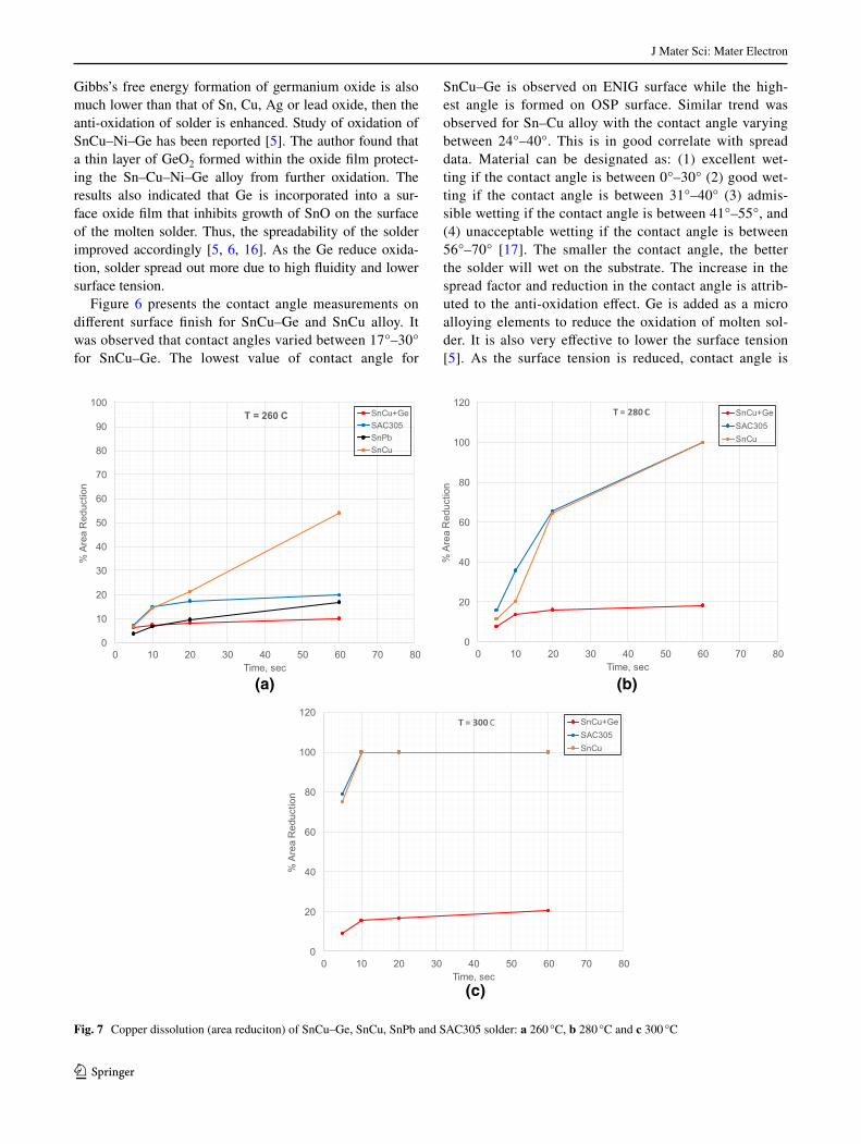
3.3 Copper dissolution
To compare the dissolution rate for different alloys, cross section was performed. Area measurement after disso-lution test were made using optical microscope and the remaining area was compared to original unexposed area. The traces copper dissolution results for SAC305, SnCu, SnPb and SnCu–Ge alloys are shown in Fig. 7 at 260, 280, and 300 °C, respectively. Corresponding cross sectional results are illustrated in Fig. 8. At 260 °C, the area of trace for SAC305 and SnCu was reduced by 18 and 32% within 20 s while for SnCu–Ge alloy, area was reduced by only 8%. The area reduction at 60 s for SAC305 and SnCu was 20 and 54%, and corresponding reduction for SnCu–Ge was 10%. The dissolution rate was found to increase linearly with temperature and var-ies between the different alloys. At 280 °C (Fig. 8), after 20 s exposure time, the area reduction for SnCu and SAC305 was 65 and 16% for SnCu–Ge. After 60 s of exposure time, copper is completely dissolved by SnCu
(3)Fmax
= c�ls cos � − �gv
and SAC305 alloy. On the other hand, area reduction for SnCu–Ge alloy was only 19% at the same conditions. At 300 °C, copper is completely dissolved after 10 s for SnCu and SAC305 alloy and for SnCu–Ge area reduc-tion was only 21% even after 60 s of exposure time. From these results, it is evident that SnCu–Ge have the low-est copper dissolution compared to SnCu and SAC305 alloy even with the highest exposure time and at higher temperature.
Dissolution rates calculated from the slope of the trace dissolution data are plotted in Fig. 9. At 260 °C, SnCu–Ge have copper dissolution rates of 0.06 mil/s compared to 0.057 mil/s for the SnPb solder. On the other hand, SnCu and SAC305 have dissolution rates of 0.14 and 0.12 mil/s which is approximately double of SnCu–Ge. It is also noted that dissolution rate increased with temperature. Figure 10 summarized the dissolution rate as a function of temperature. At 280 and 300 °C, dissolution rate of SnCu–Ge alloy was 0.11 and 0.13 mil/s and for SnCu and SAC305 alloys, rates were between 0.48 and 1.46 mil/s. Based on the analysis, SnCu–Ge could be superior candi-dates for lead free wave soldering as well as selective sol-dering process with a great improvement in reduction of copper dissolution. In wave/selective soldering process, it is expected to dissolve copper from the board pads, traces, and component. The solubility of copper in lead free solder is higher than that of SnPb solder. Exposed copper surface can be removed completely, disconnecting the land from the track. For critical application, selection
Fig. 8 Copper trace dissolution of SnCu-Ge, SnCu, SnPb and SAC305 solder: a 260 °C, b 280 °C and c 300 °C

J Mater Sci: Mater Electron
1 3
of alloy with low copper dissolution would increase the chance of reliable solder joints. However, in real wave soldering process, copper dissolution depends on flow dynamics which could have significant impact on the rate of dissolution.
The copper dissolution is a diffusion controlled process and very well documented. Along with the type of alloy, temperature, flow conditions, copper dissolution also depends on intermetallic formation. IMC formation occurs at copper side and in the presence of a IMC, less copper will leave the Cu/IMC substrate effectively reducing the copper dissolution rate. IMC act as a barrier for copper diffusion. Cu dissolution is also dependent on solder fluid-ity/viscosity and wetting characteristics along with other factors. However, another reason come down to sluggish
wetting behavior of solder controls the copper dissolution because of the elongated wetting time and temperature. As discussed in previous section, addition of Ge acts as an antioxidant, reduce the surface tension and increase the wetting performance thus shorter the contact time. So, the benefit of wetting time (shorter time) might reduce the cop-per dissolution. When a copper is in contact with molten solder, less number of copper atoms will tend to diffuse into the molten solder due to shorter wetting time. There-fore, dissolution rate will decrease.
3.4 Microstructural analysis
Figure 11 depicts the polarized micrograph of SnCu–Ge and SnCu alloy. SnCu–Ge exhibits the fine grain structure
(b)(a)
(c)
0
0.5
1
1.5
2
2.5
3
0 5 10 15 20 25
Red
uctio
n in
Cu
Wire
Dia
met
er, m
il
Time, sec
260 CSAC305
SnPb
SnCu+Ge
SnCu
Fit - SAC305
Fit - SnPb
Fit- SnCu+Ge
Fit- SnCu
Rate = 0.14 mil/sec
Rate = 0.12 mil/sec
Rate = 0.06 mil/sec
Rate = 0.057 mil/sec
0
2
4
6
8
10
12
14
0 5 10 15 20 25
Red
uctio
n in
Cu
Wire
Dia
met
er, m
il
Time, sec
280 CSAC305
SnCu+Ge
SnCu
Fit - SAC305
Fit- SnCu+Ge
Fit- SnCu
Rate = 0.49 mil/sec
Rate = 0.48 mil/sec
Rate = 0.11 mil/sec
0
5
10
15
20
25
30
35
0 5 10 15 20 25
Red
uctio
n in
Cu
Wire
Dia
met
er, m
il
Time, sec
300 CSAC305
SnCu+Ge
SnCu
Fit - SAC305
Fit-SnCu+Ge
Fit- SnCu
Rate = 1.41 mil/sec
Rate = 1.46 mil/sec
Rate = 0.13 mil/sec
Fig. 9 Copper dissolution rate of SnCu–Ge, SnCu, SnPb and SAC305 solder: a 260 °C, b 280 °C and c 300 °C

J Mater Sci: Mater Electron
1 3
and the precipitation of Cu6Sn5 intermetallic compound. Figure 12 shows backscattered electron micrograph of SnCu–Ge and SnCu solder alloy. EDS was carried out to determine the elemental distribution and IMC formation. The microstructure consists as a eutectic tin rich phase and well dispersed Cu6Sn5 particles. It is noted that addi-tion of minor Ge change the morphology of the micro-structure. Ge rich precipitation was not form in the alloy as the addition of Ge was only 0.01%. Moreover, addition of traces Ge leads to refine the grain structure compared to SnCu, resulting in improved cast ability. IMC layers was also examined between solder and copper substrate. IMC thickness was determined using an area average method. IMC area and horizontal length is measured over the measurement window and the IMC thickness is obtained by dividing the area of the IMCs by the length of the IMCs over the measurement window (Fig. 13). IMC thickness measurement was facilitated by using image processing software on images taken from ESEM.
0
0.2
0.4
0.6
0.8
1
1.2
1.4
1.6
1.8
2
240 250 260 270 280 290 300 310
Dis
solu
tion
Rat
e, m
il/se
c
Temperature, C
SAC305SnPbSnCu+GeSnCu
Fig. 10 Static copper dissolution rate vs temperature of SnCu–Ge, SnCu, SnPb and SAC305 solder
Fig. 11 Polarized micrograph of SnCu–Ge and SnCu solder
Fig. 12 Backscattered scanning electron micrographs of SnCu–Ge and SnCu solder alloy

J Mater Sci: Mater Electron
1 3
Four measurements are made for each condition, average of these reading is reported. Standard deviation has been added to the data. IMC thickness on Cu substrate was 1.64 and 2.43 µm for SnCu–Ge and SnCu alloy, respec-tively after reflow (Fig. 14). A thin, continuous, and uniform IMC layer is an essential requirement for good bonding while acting as a barrier to copper diffusion. However, a thick IMC layer at the interface may degrade the reliability of the solder joints because of their brittle nature. EDS analysis confirms the formation of uniform IMC layers at interface. It was also observed from EDS analysis that Ge didn’t form any IMC, thus it could be assumed that Ge is absorbed onto the surface of the IMC (Fig. 15). Scallop type thin layer of IMC was observed on copper substrate which didn’t protrude substantially into the bulk solder. IMC layer was uniform and Ge didn’t
have any effect on growth direction of IMC. There was no IMC spalling on the Cu substrate.
Effect of multiple reflows on the IMC formation has been investigated. Figure 16 shows the IMC formation in SnCu–Ge alloy after five times reflow. IMC layer grew up to only about 1.64, 2.46, 2.23, 2.15, and 3.21 µm, respec-tively after each additional reflow. The morphology of the IMC remains unchanged. Even after five reflow, only Cu6Sn5 IMC formed at the interface. These results con-firm the microstructural stability. We believe this is due to increased wetting performance of SnCu–Ge solder thus suppressed the further IMC growth.
3.5 Tensile test results
Room temperature tensile tests have been performed at three different strain rates. The tensile properties nearly lin-ear with strain rates. There is a linear relationship between ultimate tensile strength and strain rate, and this relation-ship can be expressed by Eq. (1):
where m is the strain-rate sensitivity factor, �̇� is the strain rate, C is the material constant, and σ is the ultimate ten-sile strength. The m value calculated for this alloy was 0.117. The strain rate sensitivity value m indicates the capacity to resist necking [18, 19]. Thus, we could expect that SnCu–Ge alloy would present a tolerable resistance to necking. Figure 17 summarized the linear relationships between tensile properties and strain rates. Ultimate ten-sile strength and yield stress increase with the increment of strain rate. A significant increase in the elongation (45%) was noticed for SnCu–Ge alloy compared to SnCu alloy (35%) (Fig. 18). This means ductility of SnCu–Ge is higher
(3)𝜎UT = C �̇�m
Fig. 13 Interfacial IMC thickness measurement
Fig. 14 IMC layers in SnCu–Ge and SnCu solder on Cu substrate after reflow

J Mater Sci: Mater Electron
1 3
than SnCu alloy. It also means that SnCu–Ge can accom-modate the strain without embrittlement compared to SnCu alloy.
3.6 Hardness test results
Hardness test results revealed that addition of Ge increase the micro hardness value of SnCu–Ge compared to SnCu alloy (Fig. 19). This is likely due to refinement of the grain structure and uniform distribution of IMC. Previous study [7] also confirmed that addition of trace of Ge significantly improve the Sn3.5Ag solder pull and ball shear strength. Figure 20 illustrates the hardness impression of SnCu–Ge and SnCu alloy. It is evident from the micrograph that hard-ness impression was large enough to cover all the phases of the solder materials. Thus, hardness test characterized the global properties of the solder rather than individual properties in the different phases such as β-tin or Cu6Sn5 intermetallic.
4 Conclusions
SnCu–Ge alloy offers superior wetting and spreading perfor-mance over SnCu alloy. Addition of Ge improves the solder wetting performance (lower the wetting time, total wetting time and increase wetting force) as a function of tempera-ture compared to SnCu alloy. Lower Wetting time and higher wetting force reflects better wetting performance correlate to spread and fillet formation under a given soldering process. SnCu–Ge solder spreadability on different surface finishes
Fig. 15 EDS analysis of IMC layers in SnCu–Ge solder
Fig. 16 SnCu–Ge solder IMC layers on Cu substrate after five reflows

J Mater Sci: Mater Electron
1 3
Strain Rate, 1/sec
0.0001 0.001 0.01 0.1 1
Ulti
mat
e Te
nsile
Stre
ngth
, MPa
0
10
20
30
40
50
60SnCu+Ge
SnCu
Strain Rate, 1/sec
0.0001 0.001 0.01 0.1 1
Frac
ture
Stra
in, %
0.2
0.3
0.4
0.5
0.6SnCu+GeSnCu
Strain Rate, 1/sec
0.0001 0.001 0.01 0.1 1
Yie
ld S
treng
th, M
Pa
0
10
20
30
40
50
60SnCu+GeSnCu
(a) (b)
(c)
Fig. 17 SnCu–Ge and SnCu solder (a) tensile strength (b) yield strength and (c) fracture strain (ductility) at various strain rates
0
5
10
15
20
25
30
35
40
45
50
0 0.01 0.02 0.03 0.04 0.05 0.06
Stre
ss, M
Pa
Strain
SnCu-GeSnCu
Fig. 18 Typical stress–strain curve showing improved ductility of SnCu–Ge solder alloy
0
2
4
6
8
10
12
14
16
18
20
uCnSeG+uCnS
Mic
roha
rdne
ss
Fig. 19 Microhardness of SnCu–Ge and SnCu solder alloy

J Mater Sci: Mater Electron
1 3
(OSP, ENIG, ImAg) has been increased significantly com-pared to SnCu alloy. The largest spread was noted for ENIG finish followed by ImAg and OSP finish, respectively. Con-tact angle measurements on different surface finish varied between 17°–30°. SnCu–Ge alloy has the lowest copper dis-solution compared to SnCu and SAC305 alloy even with the highest exposure time and at higher temperature. At 280 °C, after 20 s exposure time, the area reduction for SnCu was 65% while that was only 16% for SnCu–Ge alloy. At 300 °C, copper is completely dissolved after 10 s for SnCu alloy and for SnCu–Ge alloy, area reduction was only 21% even after 60 s of exposure time. This is great improvement and have important implication in wave soldering process where tem-perature goes up to 400 °C for thick PCB application. A thin and uniform IMC was observed on different substrate. IMC size didn’t grow significantly after multiple reflows. The ten-sile testing results showed the increase in tensile strength and tolerable ductility. Thousands of boards/connectors were assembled using this alloy and demonstrated as a cost advan-tage, dross removal and able to create reliable defect free process. Future work will be focusing on thermo-mechanical reliability, vibration and drop/shock performance and will be published later.
Acknowledgements This research was supported by Kester R & D, material science division. The authors thankful to ITW Tech Center and Buehler for sample preparation and analysis.
References
1. M. Abtew, G. Selvaduray, Lead free solders in microelectronics. Mater. Sci. Eng. R 27, 95–141 (2000)
2. J.W. Evans, A Guide to Lead-Free Solders: Physical Metallurgy and Reliability, Springer, New York, 2007
3. H.Z. Huang, X.Q. Wei, D.Q. Tan, L. Zhou, Effects of phospho-rus addition on the properties of Sn–9Zn lead free solder alloy. Int. J. Miner. Metall. Mater. 6, 563–567 (2013)
4. A. Xian, G.L. Gong, Oxidation behavior of molten tin doped with phosphorus. J. Electron. Mater. 12, 1669–1678 (2007)
5. K.M. Watling, A. Chandler-Temple, K. Nogita, XPS analysis of oxide films on lead free solders with trace additions of ger-manium and gallium. Mater. Sci. Forum 857, 63–67 (2016)
6. X. Yan, K. Xu, J. Wang, X. Wei, W. Wang, Effect of P and Ge doping on microstructure of Sn-0.3 Ag-0.7 Cu/Ni–P solder joints, Soldering Surf. Mount Technol. 28, 215–221 (2016)
7. E.P. Leng, W.T. Ling, N. Amin, I. Ahmad, T.Y. Han, C.W. Chiao, A.S.M.A. Haseeb, BGA lead free C5 solder system improvement by Germanium addition to Sn3.5Ag and Sn-3.8 Ag-0.7 Cu solder alloy. in Electronics Packaging Technology Conference, pp. 82–91, 2009
8. M.G. Cho, S.K. Seo, H.M. Lee, Undercooling, microstructures and hardness of Sn-rich Pb-free solders on Cu-xZn alloy under bump metallurgies. Mater. Trans. 50, 2291–2296 (2009)
9. A. Sharif, Y.C. Chan, Dissolution kinetics of BGA Sn–Pb and Sn–Ag solders with Cu substrates during reflow. Mater. Sci. Eng. B 106, 126–131 (2004)
10. F. Byle, D. Jean, D. Lee, A study of copper dissolution in Pb-Free solder fountain systems, in Proceedings of SMTA Interna-tional, 2006
11. D. Maio, C.P. Hunt, On the factors affecting the dissolution of copper in molten lead free solders and development of a method to assess the soldering parameters. Soldering Surf. Mount Technol. 21, 24–31 (2009)
12. J.F. Li, S.H. Mannan, M.P. Clode, D.C. Whalley, D.A. Hutt, Interfacial reactions between molten Sn–Bi–X solders and Cu substrates for liquid solder interconnects. Acta Mater. 54, 2907–2922 (2006)
13. G. Humpston, D.M. Jacobson, Solder spread: a criterion for evaluation of soldering. Gold Bull. 3, 83–96 (1990)
14. P.T. Vianco, An overview of surface finishes and their role in printed circuit board solderability and solder joint perfor-mance. Circ. World 25, 6–24 (1999)
15. M.F. Arenas, V.L. Acoff, Contact angle measurements of Sn–Ag and Sn–Cu lead free solders on copper substrates. J. Elec-tron. Mater. 12, 1452–1458 (2004)
Fig. 20 Hardness impression of SnCu–Ge and SnCu solder alloy

J Mater Sci: Mater Electron
1 3
16. S.H. Wang, T.S. Chin, C.F. Yang, S.W. Chen, C.T. Chuang, Pb-free solder alloy based on Sn–Zn–Bi with the addition of germa-nium. J. Alloys Compd. 497, 428–431 (2010)
17. R.J.K. Wassink, Soldering in Electronics: A Comprehensive Treatise on Soldering Technology for Surface Mounting and Through Hole Techniques, Electrochemical Publications, Scot-land, 1994
18. R.W. Hertzberg, Deformation and Fracture Mechanics of Engi-neering Materials, 4th edn. Wiley, New York, 1996
19. F. Lang, H. Tanaka, O. Munegata, T. Taguchi, T. Narita, The effect of strain rate and temperature on the tensile properties of Sn–3.5 Ag solder. Mater. Charact. 54(3), 223–229 (2005)