effect of back mold grooves on improving uniformity in nanoimprint lithography
TRANSCRIPT

This content has been downloaded from IOPscience. Please scroll down to see the full text.
Download details:
IP Address: 147.188.128.74
This content was downloaded on 12/11/2014 at 01:08
Please note that terms and conditions apply.
Effect of Back Mold Grooves on Improving Uniformity in Nanoimprint Lithography
View the table of contents for this issue, or go to the journal homepage for more
2007 Jpn. J. Appl. Phys. 46 6370
(http://iopscience.iop.org/1347-4065/46/9S/6370)
Home Search Collections Journals About Contact us My IOPscience

Effect of Back Mold Grooves on Improving Uniformity in Nanoimprint Lithography
Hong HOCHENG� and Wei Hsuan HSU
Department of Power Mechanical Engineering, National Tsing Hua University,
101, Section 2 Kuang Fu Road, Hsinchu, Taiwan 30013, R.O.C.
(Received October 25, 2006; revised June 18, 2007; accepted June 22, 2007; published online September 20, 2007)
The nanoimprint technique has the advantages of high throughput, sub-10-nm resolution and low cost. However, thenonuniform surface obtained in practice raises concerns about the quality of pattern transfer. In this study, we present auniform printing method across a wafer by introducing a local mold deformation along the block boundary. This method issimple and effective: it involves cutting grooves on the back of the mold within the nonpatterned area. The grooves enable themold to lie easily on the substrate with a close fit to obtain a more uniform pattern over a large surface. The proposed methodwas demonstrated experimentally. [DOI: 10.1143/JJAP.46.6370]
KEYWORDS: nanoimprint, imprint lithography, grooves, uniformity, aspect ratio
In the past 40 years, industrial technology has followedMoore’s law for semiconductors and ICs. The crucialtechnology of photolithography has influenced the linewidth that is to be exposed. However, when the patternfeature size becomes smaller than 100 nm, photolithographybecomes difficult. The line width is limited by wavelengthdiffraction, posing a challenge to physicists. The cost of themanufacturing process and exposing equipment will increasewhen the pattern size decreases further. For this reason, alow-cost and high-throughput process for manufacturingnanostructures is essential.
The semiconductor industry works hard at tracking everyaspect of technology in order to enable the industry to followMoore’s law. Using a 193 nm light source in coordinationwith immersion technology, optical proximity correction(OPC) and the use of a phase shift mask (PSM) can exposethe pattern of 65 and 45 nm nodes; nevertheless, 32 nm nodetechnology is still to be developed. There are variouspotential methods for achieving 32 nm node technology: oneis to develop a shorter wavelength of the light source usedfor exposure, and the other is nanoimprint lithography (NIL).NIL allows the fast replication of nanoscale patterns and is apromising technique with wide applications, including thefabrication of electronic devices, biosensors, microchannels,high-density memory disks and optical devices. However, tomake this technology suitable for industrial use, not only ahigh resolution but also reliable patterning over a large areamust be achieved.
NIL was first reported by Chou et al. in 19951) and hasdeveloped over the last ten years, and there are threeobjectives to be achieved, namely, imprinting in nanoscaledimensions,2) fabricating structures with a high aspectratio,3) and imprinting over a large area.4) However, thesethree objectives have barely been satisfied simultaneously todate.
In NIL, the resist is patterned by physical deformationusing a mold. Therefore, the profile of the mold surface deter-mines the imprinted pattern. Most studies use a mold thatfeatures patterns protruding from the datum plane of themold. It is difficult to fabricate the pattern for this kind ofmold, which usually involves the lift- off process after NIL,when the critical dimension decreases to 100 nm. When thepattern feature size is less than 100 nm, an etching processis substituted for the lift- off process. If one uses etching after
NIL, the mold of the imprinting process will feature the pat-tern indented in the datum plane of the mold. This kind ofmold in NIL requires a higher pressure than the mold that fea-tures patterns protruding from the datum plane of the mold.
However, using a high pressure will lead to molddeformation in the patterned area and nonuniformity in theimprinted pattern. For the same reason, using this kind ofmold to imprint on a large area is even more difficult. A fewkey difficulties of this lithography must be overcome inorder to make it a sophisticated technique for industrial use.
In the commonly practiced thermal nanoimprint process-es, the material of the mold and substrate is silicon wafer.The surface quality of the silicon wafer is defined by totalthickness variation (TTV) and bow/warp. Typical valuesof TTV and bow/warp are about 20 and 60 mm, respectively.This quality is not ideal for the imprinting process of a nano-scale pattern; therefore, a high imprint pressure is needed toensure the complete pattern transfer. However, the high im-print pressure causes mold deformation. In the imprintingprocess, such a mold deformation occurs in both patternedand nonpatterned areas.5) If the mold deformation occursin the patterned area, it will induce not only poor patternquality, but also a nonuniform residual layer, on which theplasma etching after imprinting becomes very difficult.
As mentioned before, NIL enables us to rapidly replicate ananoscale pattern. It provides the possibility of challengingMoore’s law. Up to now, NIL has been unable to prevent theformation of defects over a large area in a single imprintingstep. This problem has limited its wide application. In thisstudy, we aim to increase the uniformity over a largeimprinted area and also fabricate a high-aspect-ratio pattern.
A newly designed local mold deformation method wasadopted to improve the imprinting uniformity. The moldused in this method has thick rigid imprinting areasassociated with thin cut grooves, which provide the desiredflexibility for imprinting. The mold design is shown inFig. 1. On the back of the mold, the grooves are cut withinthe nonpatterned area. One can use these back grooves in theimprinting process to produce the designed deformationacross the mold. This mold deformation is concentrated inthe nonpatterned area and helps reduce the mold deforma-tion in the patterned area. The imprinting uniformity is thusimproved. The imprinting pressure can also be effectivelylowered.
In the experiment, the mold is obtained by electron-beamlithography on a 4-in. silicon wafer. Each patterned area is�E-mail address: [email protected]
Japanese Journal of Applied Physics
Vol. 46, No. 9B, 2007, pp. 6370–6372
#2007 The Japan Society of Applied Physics
6370
Brief Communication

10� 0:15mm2 and contains 50 nm lines with 50 nm spacingand has a height of 200 nm. The pattern is indented in thedatum plane. The mold is covered with a surfactant,octadecyl-chlorosilane, CH3–(CH2)17–SiC13 (OTS), whichpromotes polymer release from the mold in the demoldingprocess.
The polymer is one of the key parameters for NIL, whichrequires polymers with stable thermal properties and goodetch resistance. In this study, the commercial resist mr-I8030designed for NIL is selected and applied on a 4-in. siliconwafer with 20 mm TTV and 60 mm bow/warp. The glasstransition temperature is 125 �C. The decomposition of thepolymer is characterized by an endothermic peak appearingabove 200 �C.6) The printing conditions using this polymerare lower than 200 �C and 10MPa.
A special mold is prepared for the proposed technique.The relative positions of the pattern and grooves are shownin Fig. 2. The width and depth of the grooves are 150 and300 mm, respectively. The grooves are cut perpendicular toeach other; one direction is parallel to the flat edge of thewafer, the other is vertical. The area of each square blockseparated by the grooves is 200mm2.
In the imprinting experiment, not only a suitable range ofimprinting conditions needs to be identified but also animprovement using the back grooves needs to be demon-strated. In ref. 3, the imprinting pressure increased when theaspect ratio of the mold cavity increased. The effect ofpressure on the high-aspect-ratio structure was particularlyevident in this study; in the imprinting experiment, the moldwas imprinted at 2.5, 5.0, and 7.5MPa. Also, it has beendemonstrated that increasing the imprinting time canincrease the imprint uniformity.6) Therefore, the imprinted
time is increased from 1 to 7min in this imprintingexperiment. After imprinting, the cross sections of theimprinted pattern are examined by scanning electron mi-croscopy (SEM).
The experimental results show that patterning a high-aspect-ratio structure with nanoscale dimensions over a largearea is difficult. The results show that during imprinting, thepolymer cannot fill the mold cavity in each patterned areawithin 1min. Even upon increasing the imprinting force, thefilling is not improved markedly.
On the basis of the imprinting results, one can obtain thebest imprinting structure at a pressure of 7.5MPa when theimprinting time is 7min. Nevertheless, patterning theimprinted structures in each area is still rather difficult.Because high pressure leads to mold deformation, andsubstrate distortion occurs during the imprinting, theeffective imprinting area increases but the imprinting qualityis adversely affected.
Either high-aspect-ratio or large-area imprinting requireshigher pressure. When the aspect ratio of the imprintedpattern becomes higher than 2, not only must the imprintingpressure be increased, but also the number of defectsincreases during demolding. The polymer pattern is oftenbroken at the bottom, particularly for an aspect ratio as highas 3.3) The high imprinting pressure causes the concentrationof stress at the bottom corner of the printing pattern leadingto this kind of defect. In order to avoid such defects, thesurface energy of the mold and the side-wall roughness ofthe mold cavity need to be decreased. In addition, reducingthe imprinting force can decrease the stress concentration atthe bottom corner of the imprinted structure.
The aforementioned results reveal that using high pressureover a large imprinted area easily lead to substrate distortionand affects the imprinting quality significantly. In order tosolve this problem, the proposed structure of grooves isadded to the back of the imprinted mold, as shown in Fig. 2.
There are six patterned areas in the imprinted mold(Fig. 2), and each patterned area is observed after imprint-ing. From these observations, the imprinted results of twopatterns 50mm apart and facing each other, A and D inFig 2, are shown in Figs. 3 and 4. Figures 3(a) and 3(b)show the results at 180 �C, 2.5MPa, and 7min. Figure 4shows the results at 180 �C, 7.5MPa, and 7min. Thetechnique using back grooves allows the successful patterntransfer in each area. On the other hand, it is difficult totransfer the pattern without the back grooves under the sameconditions.
The proposed nanoimprinting technique can effectivelyreduce the required pressure. The stress concentration at the
(a)
(b)
(c)
Fig. 1. Imprint method using mold with back
grooves. (a) Mold with back grooves, (b) during
imprinting, and (c) imprinted pattern.
F
DA
CB
E
Fig. 2. Relative positions of pattern and grooves.
Jpn. J. Appl. Phys., Vol. 46, No. 9B (2007) H. HOCHENG and W. H. HSU
6371
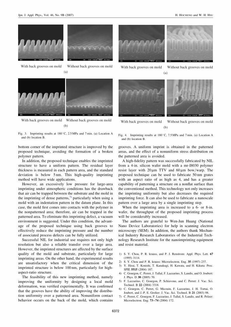
bottom corner of the imprinted structure is improved by theproposed technique, avoiding the formation of a brokenpolymer pattern.
In addition, the proposed technique enables the imprintedstructure to have a uniform pattern. The residual layerthickness is measured in each pattern area, and the standarddeviation is below 5 nm. This high-quality imprintingmethod will have wide applications.
However, an excessively low pressure for large-areaimprinting under atmospheric conditions has the drawbackthat air can be trapped between the substrate and the mold inthe imprinting of dense patterns,7) particularly when using amold with an indentation pattern in the datum plane. In thiscase, the mold first comes into contacts with the polymer inthe nonpatterned area; therefore, air can be trapped in thepatterned area. To eliminate this imprinting defect, a vacuumenvironment is suggested. Under this condition, the advant-age of the proposed technique using back grooves toeffectively reduce the imprinting pressure and the numberof associated process defects can be fully utilized.
Successful NIL for industrial use requires not only highresolution but also a reliable transfer over a large area.However, the imprinted structures are affected by the surfacequality of the mold and substrate, particularly for largeimprinting areas. On the other hand, the experimental resultsare unsatisfactory when the critical dimension of theimprinted structure is below 100 nm, particularly for high-aspect-ratio structure.
The feasibility of this new imprinting method, namelyimproving the uniformity by designing a local molddeformation, was verified experimentally. It was confirmedthat the grooves have the ability of improving the distribu-tion uniformity over a patterned area. Nonuniform contactbehavior occurs on the back of the mold, which contains
grooves. A uniform imprint is obtained in the patternedareas, and the effect of a nonuniform stress distribution onthe patterned area is avoided.
A high-fidelity pattern was successfully fabricated by NILfrom a 4-in. silicon wafer mold with a mr-I8030 polymerresist layer with 20 mm TTV and 60 mm bow/warp. Theproposed technique can be used to fabricate 50 nm grateswith an aspect ratio of as high as 4, and has a greatercapability of patterning a structure on a nonflat surface thanthe conventional method. This technology not only increasesthe imprinting uniformity but also decreases the requiredimprinting force. It can also be used to fabricate a nanoscalepattern over a large area by a single imprinting step.
When the imprinting area is increased to a 6- or 8-in.wafer, the throughput of the proposed imprinting processwill be considerably increased.
The authors are grateful to Wen-Jun Huang (NationalNano Device Laboratories) for help in scanning electronmicroscopy (SEM). In addition, the authors thank Mechan-ical Industry Research Laboratories of the Industrial Tech-nology Research Institute for the nanoimprinting equipmentand resist material.
1) S. Y. Chou, P. R. krauss, and P. J. Renstrom: Appl. Phys. Lett. 67
(1995) 3114.
2) S. Y. Chou and P. R. krauss: Microelectron. Eng. 35 (1997) 237.
3) Y. Hirai, T. Konishi, T. Kanakugi, H. Kawata, and H. Kikuta: Proc.
SPIE 5515 (2004) 187.
4) C. Gourgon, C. Perret, J. Tallal, F. Lazzarino, S. Landis, and O. Joubert:
J. Phys. D 38 (2005) 70.
5) F. Lazzarino, C. Gourgon, P. Schiavone, and C. Perret: J. Vac. Sci.
Technol. B 22 (2004) 3318.
6) C. Gourgon, C. Perret, G. Micouin, F. Lazzarino, J. H. Tortai, O.
Joubert, and J.-P. E. Grolier: J. Vac. Sci. Technol. B 21 (2003) 98.
7) C. Perret, C. Gourgon, F. Lazzarino, J. Tallal, S. Landis, and R. Pelzer:
Microelectron. Eng. 73–74 (2004) 172.
With back grooves on mold Without back grooves on mold
(a)
With back grooves on mold Without back grooves on mold
(b)
Fig. 3. Imprinting results at 180 �C, 2.5MPa and 7min. (a) Location A
and (b) location B.
With back grooves on mold Without back grooves on mold
(a)
With back grooves on mold Without back grooves on mold
(b)
Fig. 4. Imprinting results at 180 �C, 7.5MPa and 7min. (a) Location A
and (b) location B.
Jpn. J. Appl. Phys., Vol. 46, No. 9B (2007) H. HOCHENG and W. H. HSU
6372