eel 5245 power electronics i lecture #14: …fpec.ucf.edu/teaching/eel 5245...
TRANSCRIPT

EEL 5245 POWER ELECTRONICS I
Lecture #14: Chapter 4 Non-Isolated DC-DC Converters
PWM Converters DCM Analysis (DCM)
Objectives
• Overview of Discontinuous Conduction Mode • Buck Converter Analysis (DCM) • Simulation of Buck in DCM • Boost and Buck Boost Converter Analysis (DCM)
– Voltage Conversion Ratio (M=Gain) – Average Input and Output Currents – Output Voltage Ripple via Charge
approximation – Boundary Between CCM and DCM
• Examples of Analysis and Design for Boost and Buck Boost Converters in CCM/DCM
• PSPICE Simulation Verification
2
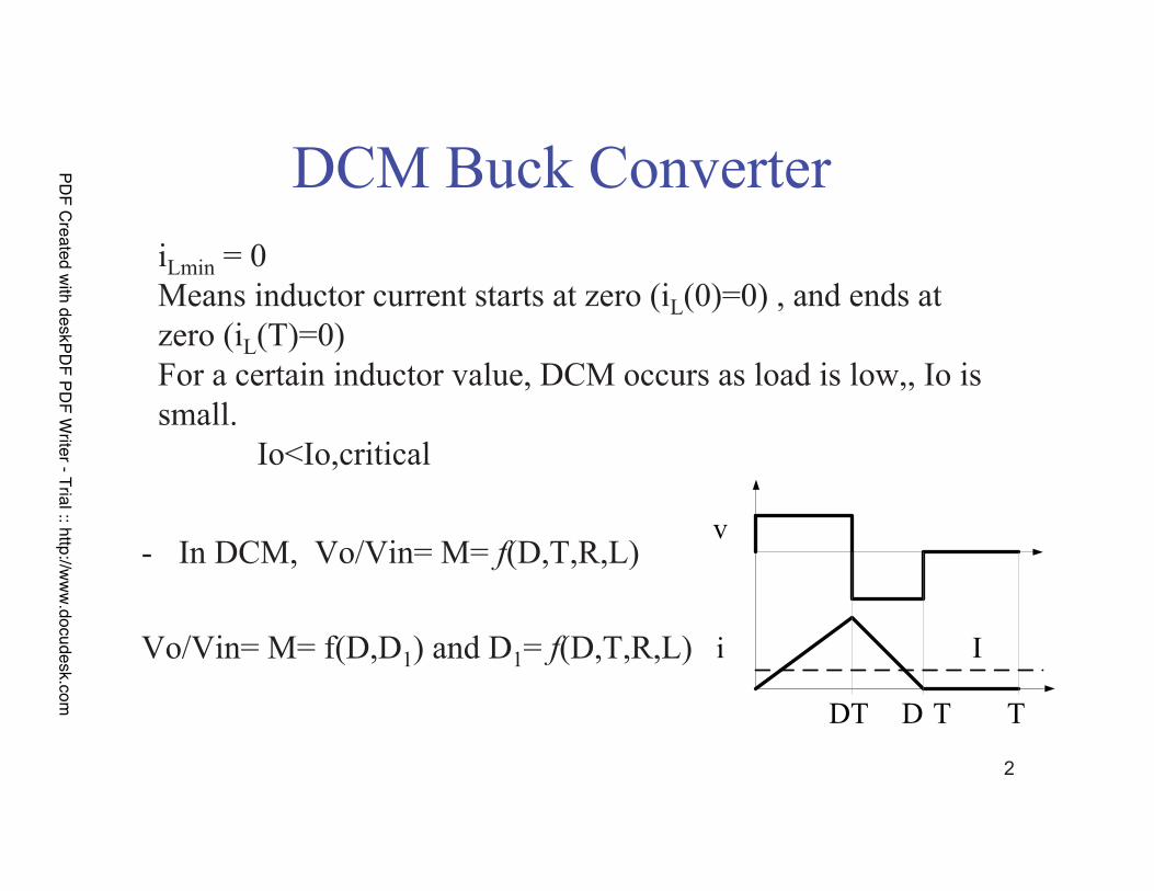
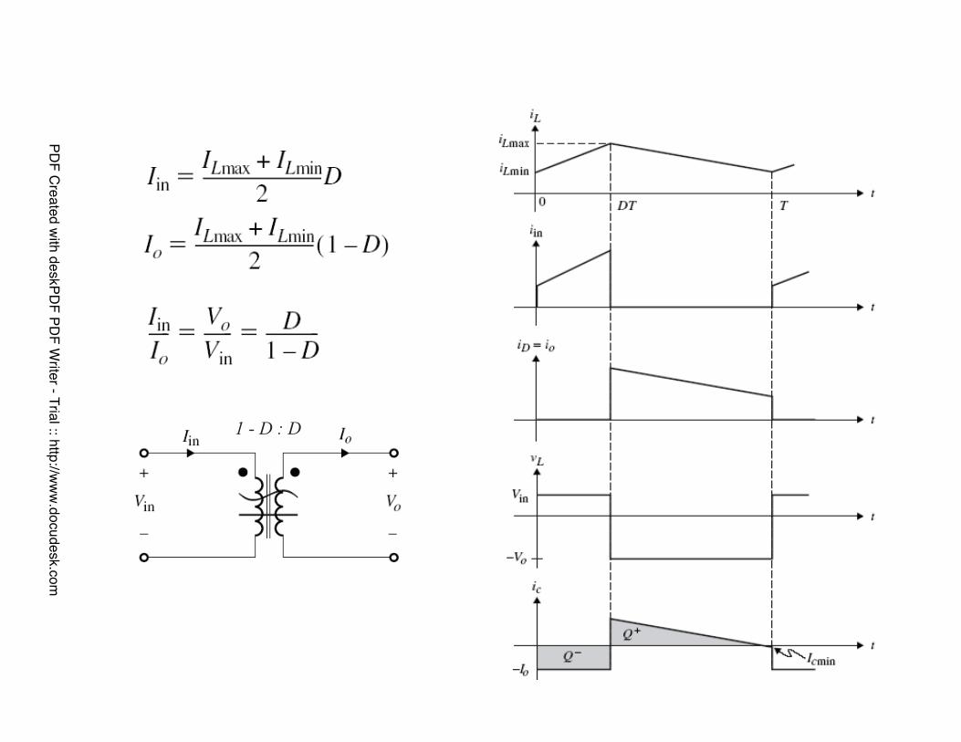
DCM Buck Converter
- In DCM, Vo/Vin= M= f(D,T,R,L)
Vo/Vin= M= f(D,D1) and D1= f(D,T,R,L)
iLmin = 0Means inductor current starts at zero (iL(0)=0) , and ends at zero (iL(T)=0)For a certain inductor value, DCM occurs as load is low,, Io is small.
Io<Io,critical
PDF C
reated with deskPD
F PDF W
riter - Trial :: http://ww
w.docudesk.com
3
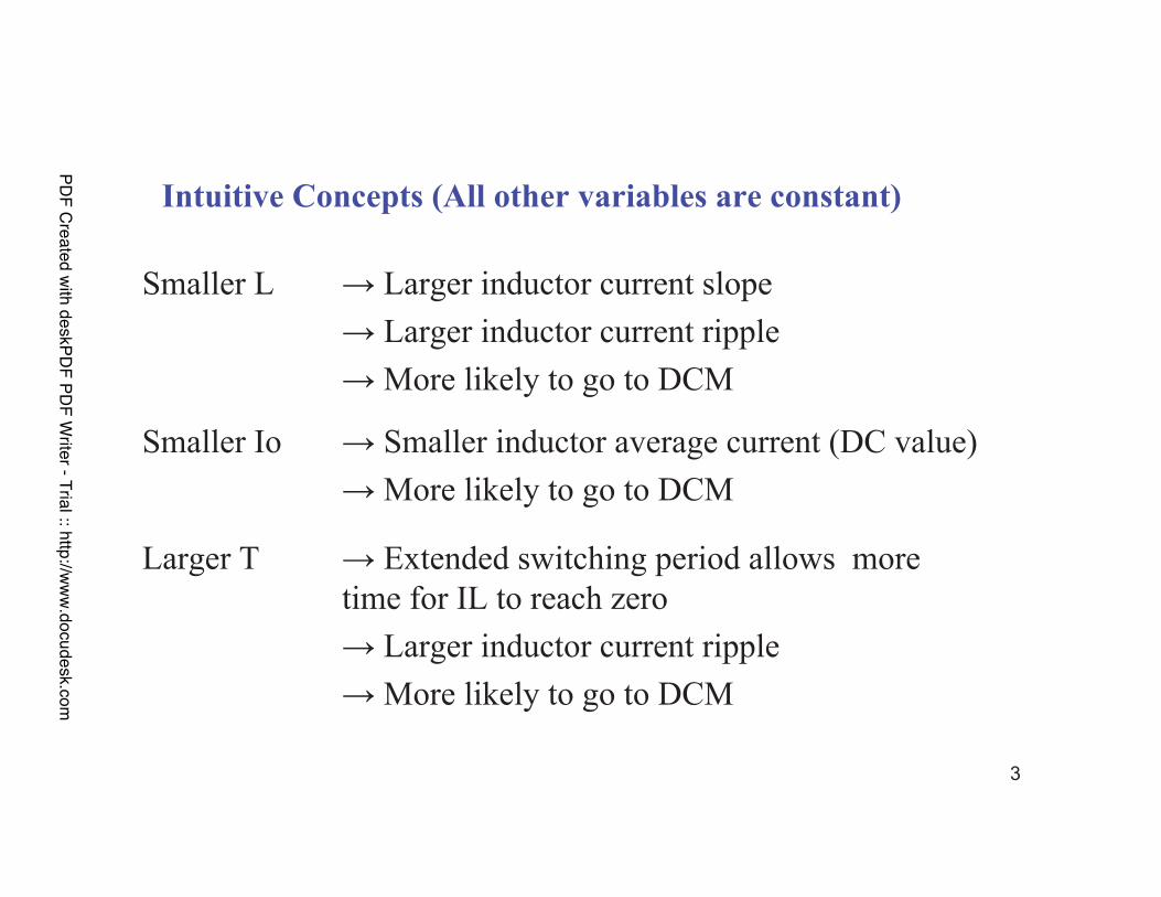
Intuitive Concepts (All other variables are constant)
Smaller L ! Larger inductor current slope
! Larger inductor current ripple
!More likely to go to DCM
Smaller Io ! Smaller inductor average current (DC value)
!More likely to go to DCM
Larger T ! Extended switching period allows more time for IL to reach zero
! Larger inductor current ripple
!More likely to go to DCM
PDF C
reated with deskPD
F PDF W
riter - Trial :: http://ww
w.docudesk.com
4
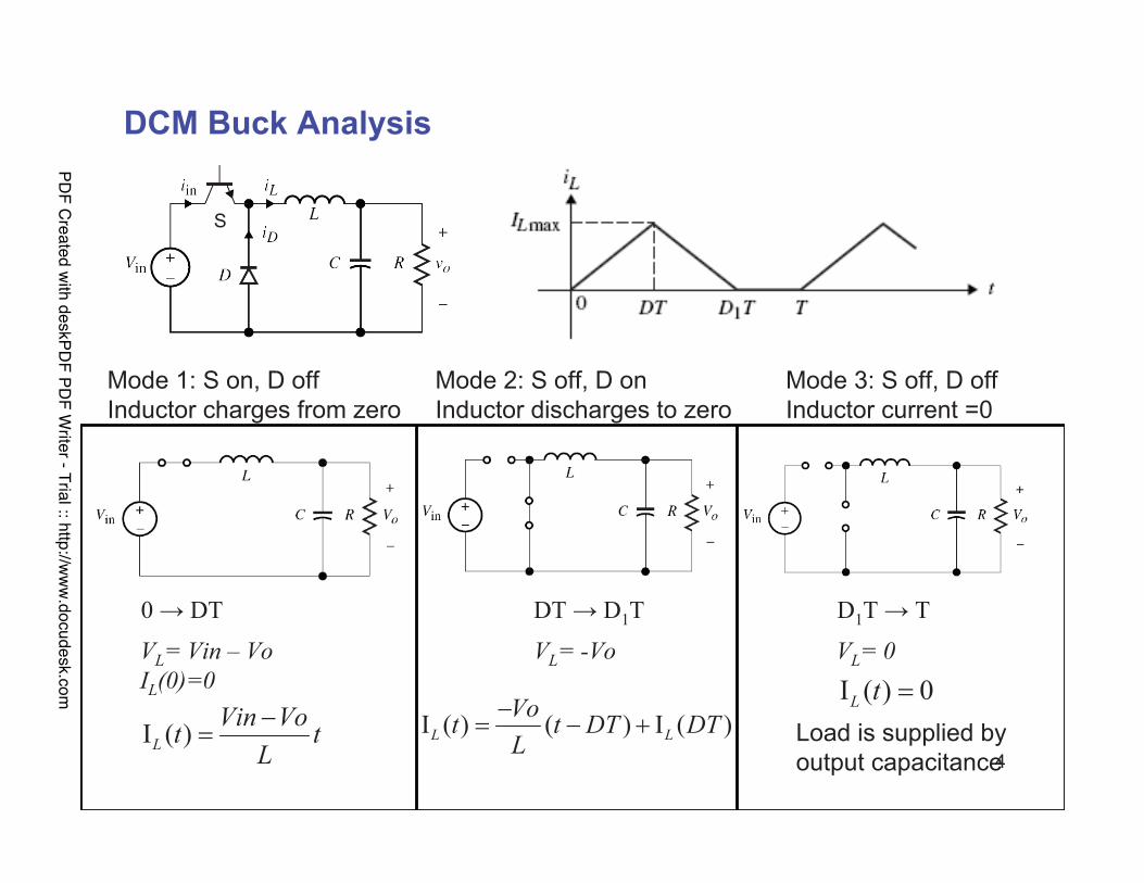
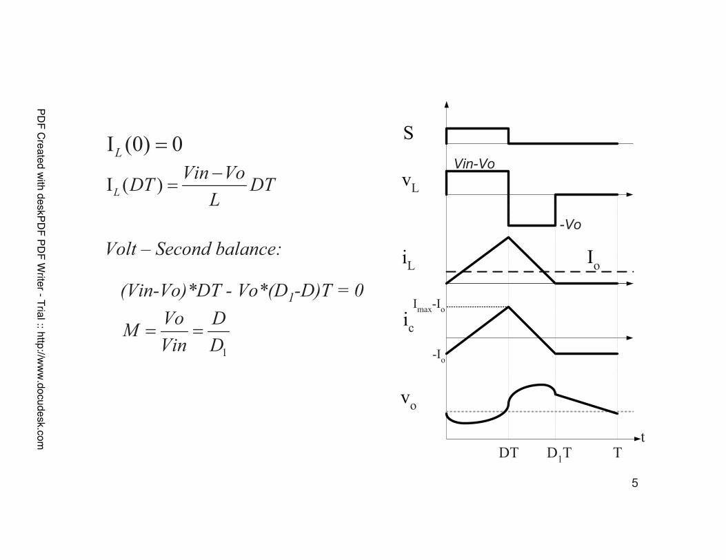
DCM Buck Analysis
0! DT DT ! D1T D1T! T
VL= Vin – VoIL(0)=0
VL= -Vo VL= 0
I ( )L
Vin Vot t
L
!" I ( ) ( ) I ( )L L
Vot t DT DT
L
!" ! #
I ( ) 0L t "
Mode 1: S on, D offInductor charges from zero
Mode 2: S off, D onInductor discharges to zero
Mode 3: S off, D offInductor current =0
S
Load is supplied by output capacitance
PDF C
reated with deskPD
F PDF W
riter - Trial :: http://ww
w.docudesk.com
5
I (0) 0L !
I ( )L
Vin VoDT DT
L
"!
L
L
c
o
tDT D
1T T
o
-Io
Imax
-Io
(Vin-Vo)*DT - Vo*(D1-D)T = 0
Volt – Second balance:
1
Vo DM
Vin D! !
Vin-Vo
-Vo
PDF C
reated with deskPD
F PDF W
riter - Trial :: http://ww
w.docudesk.com
6
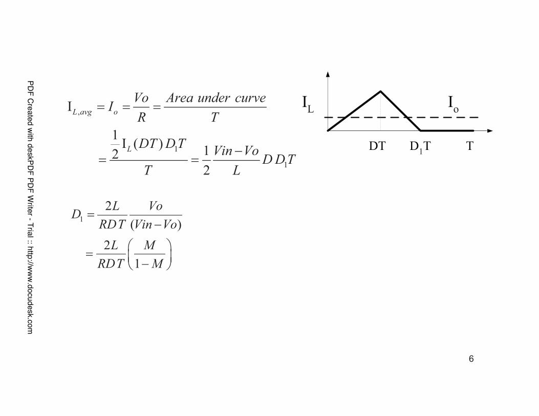
,
1
1
I
1I ( )
122
L avg o
L
Vo Area under curveI
R T
DT D TVin Vo
D D TT L
! ! !
"! !
L
1
o
1
2
( )
2
1
L VoD
RDT Vin Vo
L M
RDT M
!"
# $! % &"' (
PDF C
reated with deskPD
F PDF W
riter - Trial :: http://ww
w.docudesk.com
7
12
2
2
2 22
2
1
1 2
1
1
2
02 2
D L M
D RD T M
L M
M RD T M
RD T MM
L M
RD T RD TM M
L L
! "# $ %&' (
! "# $ %&' (
&! "# $ %
' (
) & #
2 4
2
b b ac
a
& * &
Solve for M
Find roots of M
2
2
81 1
4
D RT LM
L D RT
! "# ) &$ %$ %
' (
PDF C
reated with deskPD
F PDF W
riter - Trial :: http://ww
w.docudesk.com
8
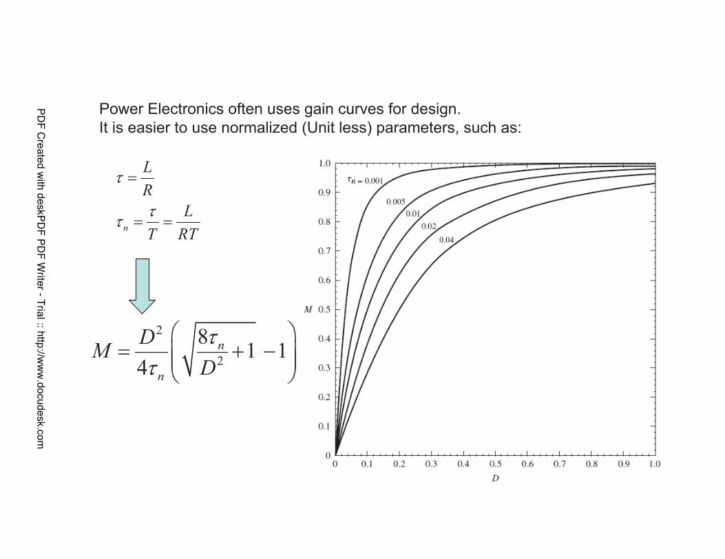
n
L
R
L
T RT
!
!!
"
" "
2
2
81 1
4n
n
DM
D
!
!
# $" % &' (' (
) *
Power Electronics often uses gain curves for design. It is easier to use normalized (Unit less) parameters, such as:
PDF C
reated with deskPD
F PDF W
riter - Trial :: http://ww
w.docudesk.com
9
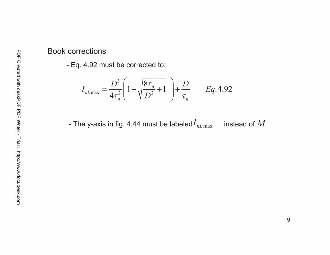
- Eq. 4.92 must be corrected to:
3
max 2 2
81 1 .4.92
4n
nL
n n
D DI Eq
D
!
! !
" #$ % & &' (' (
) *
- The y-axis in fig. 4.44 must be labeled instead of MmaxnLI
Book corrections
PDF C
reated with deskPD
F PDF W
riter - Trial :: http://ww
w.docudesk.com
10
ic
vo
t
DT D1
T T
-Io
Imax-Io
t1 t2
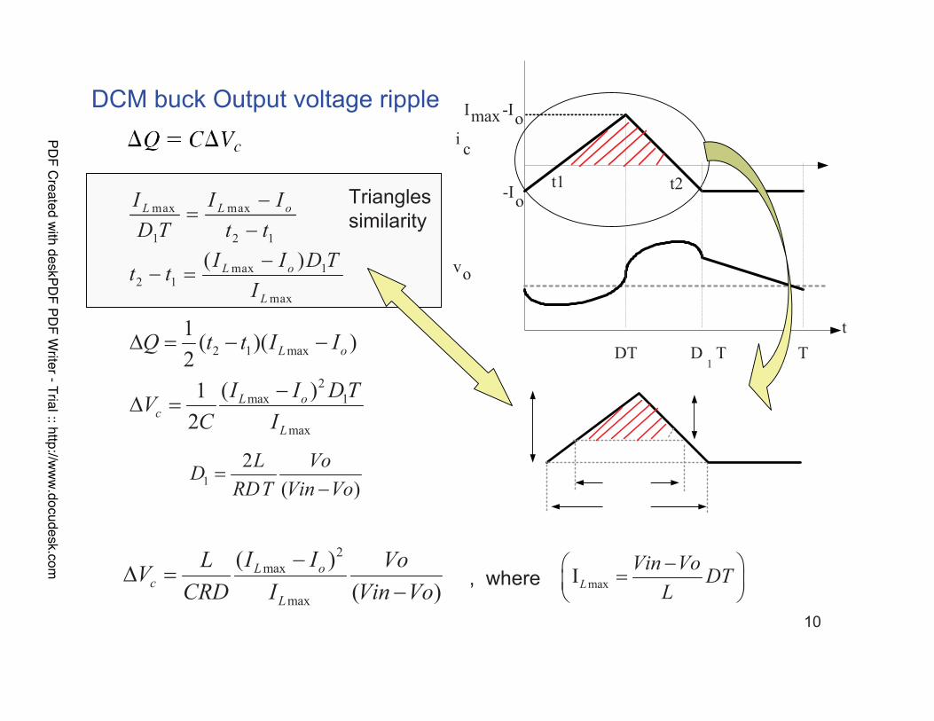
DCM buck Output voltage ripple
max max
1 2 1
L L oI I I
D T t t
!"
!
2 1 max
2max 1
max
1( )( )
2
( )1
2
L o
L oc
L
Q t t I I
I I D TV
C I
# " ! !
!# "
1
2
( )
L VoD
RDT Vin Vo"
!
2max
max
( )
( )L o
c
L
I IL VoV
CRD I Vin Vo
!# "
! maxIL
Vin VoDT
L
!$ %"& '
( )
Triangles similarity
, where
max 12 1
max
( )L o
L
I I D Tt t
I
!! "
PDF C
reated with deskPD
F PDF W
riter - Trial :: http://ww
w.docudesk.com
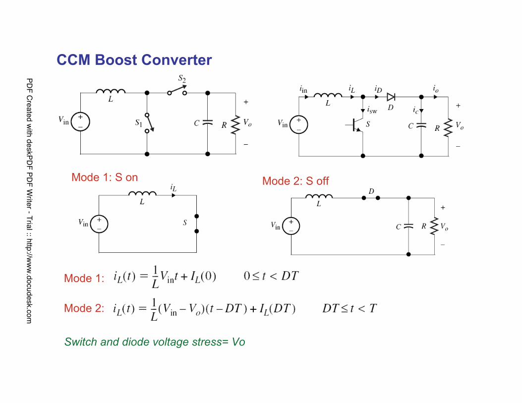
Mode 1: S on Mode 2: S off
CCM Boost Converter
Mode 1:
Mode 2:
Switch and diode voltage stress= Vo
PDF C
reated with deskPD
F PDF W
riter - Trial :: http://ww
w.docudesk.com
PDF C
reated with deskPD
F PDF W
riter - Trial :: http://ww
w.docudesk.com
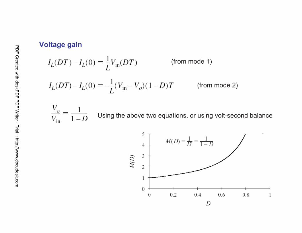
(from mode 1)
(from mode 2)
Using the above two equations, or using volt-second balance
Voltage gainPDF C
reated with deskPD
F PDF W
riter - Trial :: http://ww
w.docudesk.com
PDF C
reated with deskPD
F PDF W
riter - Trial :: http://ww
w.docudesk.com
Critical inductor
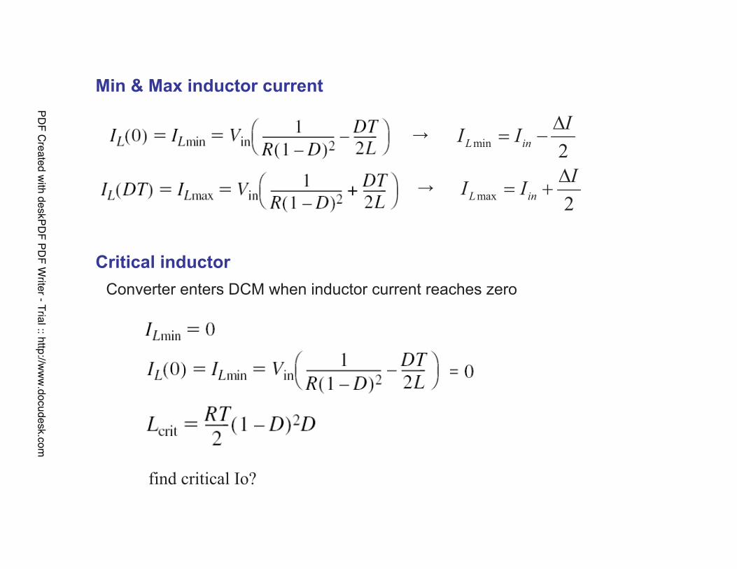
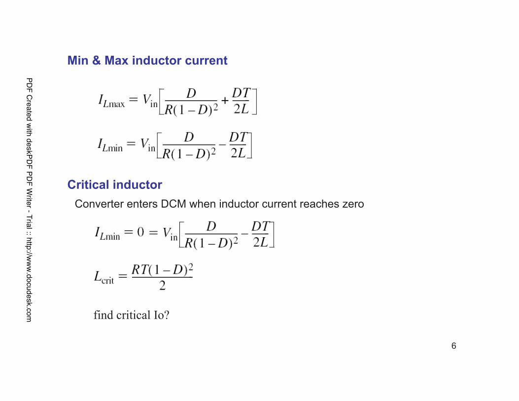
Min & Max inductor current
Converter enters DCM when inductor current reaches zero
find critical Io?
!min
2L in
II I
!" #
!max
2L in
II I
!" $
PDF C
reated with deskPD
F PDF W
riter - Trial :: http://ww
w.docudesk.com
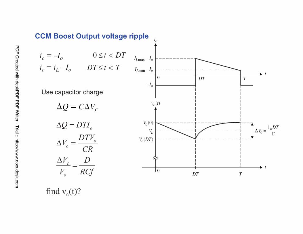
o
oc
c
o
Q DTI
DTVV
CR
V D
V RCf
! "
! "
!"
Use capacitor charge
find vc(t)?
CCM Boost Output voltage ripple
PDF C
reated with deskPD
F PDF W
riter - Trial :: http://ww
w.docudesk.com

0! DT( )L
Vini t t
L!
( ) ( ) ( )L L
Vin Voi t t DT I DT
L
"! " # DT! D1T
( ) 0Li t ! D1T!T
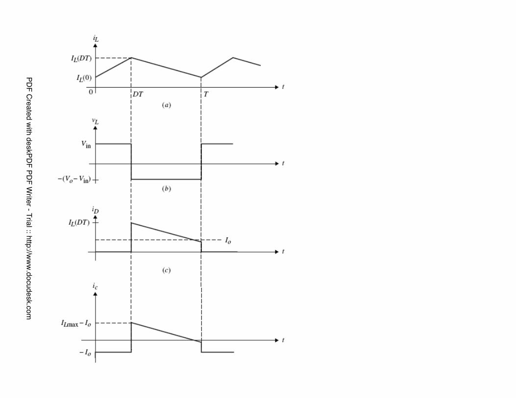
DCM Boost Converter
PDF C
reated with deskPD
F PDF W
riter - Trial :: http://ww
w.docudesk.com
0
IL
T t
vL
Vin
(Vo
Vin
)
iL
DT
iD
ic
Io
ILmax
Io
t
t
Io
D1T
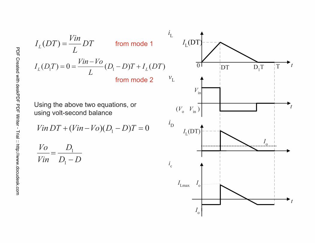
IL(DT)1( )( ) 0Vin DT Vin Vo D D T! " " #
1
1
DVo
Vin D D#
"
Using the above two equations, or using volt-second balance
( )L
VinI DT DT
L#
1 1( ) 0 ( ) ( )L L
Vin VoI D T D D T I DT
L
"# # " !
from mode 1
from mode 2
PDF C
reated with deskPD
F PDF W
riter - Trial :: http://ww
w.docudesk.com
11
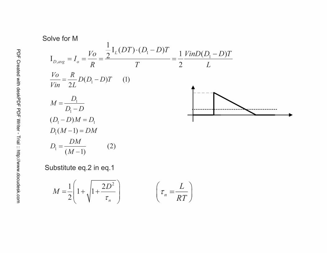
,
1I ( ) ( )
( )12I2
L
D avg o
DT D D TVinD D D TVo
IR T L
! " "# # # #
1( ) (1)2
Vo RD D D T
Vin L# "
1
1
1 1
1
1
( )
( 1)
(2)( 1)
DM
D D
D D M D
D M DM
DMD
M
#"
" #
" #
#"
Substitute eq.2 in eq.1
21 21 1
2 n
DM
$
% &# ' '( )
( )* +
n
L
RT$% &#( )
* +
Solve for M
PDF C
reated with deskPD
F PDF W
riter - Trial :: http://ww
w.docudesk.com

DCM boost output voltage ripple
max max
1 1
max 11
max
( )
( )( )
L L o
L o
L
I I I
D D T t DT
I I D D Tt DT
I
!"
! !
! !! "
1 max
2max 1
max
1( )( )
2
( ) ( )1
2
L o
L oc
L
Q t DT I I
I I D D TV
C I
# " ! !
! !# "
maxIL
VinDT
L"
Triangles similarity
1( 1)
DMD
M"
!
ic
Io
ILmax
Io
t1
t
vc
Vo
PDF C
reated with deskPD
F PDF W
riter - Trial :: http://ww
w.docudesk.com
2
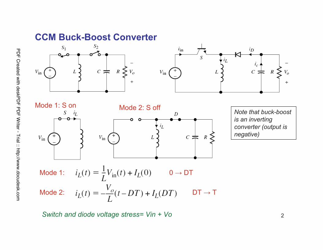
CCM Buck-Boost Converter
Mode 1: S on Mode 2: S offNote that buck-boost is an invertingconverter (output is negative)
Mode 1:
Mode 2:
0 ! DT
DT ! T
Switch and diode voltage stress= Vin + Vo
PDF C
reated with deskPD
F PDF W
riter - Trial :: http://ww
w.docudesk.com
3
PDF C
reated with deskPD
F PDF W
riter - Trial :: http://ww
w.docudesk.com

4
(from mode 1)
(from mode 2)
Using the above two equations, or using volt-second balance
0 0.1 0.2 0.3 0.4 0.5 0.6 0.7 0.8 0.9 10
1
2
33
0
M D( )
10 D
M>1
M<1
M=1
PDF C
reated with deskPD
F PDF W
riter - Trial :: http://ww
w.docudesk.com
5
1 - D : D
PDF C
reated with deskPD
F PDF W
riter - Trial :: http://ww
w.docudesk.com
6
Min & Max inductor current
Critical inductor
Converter enters DCM when inductor current reaches zero
find critical Io?
PDF C
reated with deskPD
F PDF W
riter - Trial :: http://ww
w.docudesk.com

7
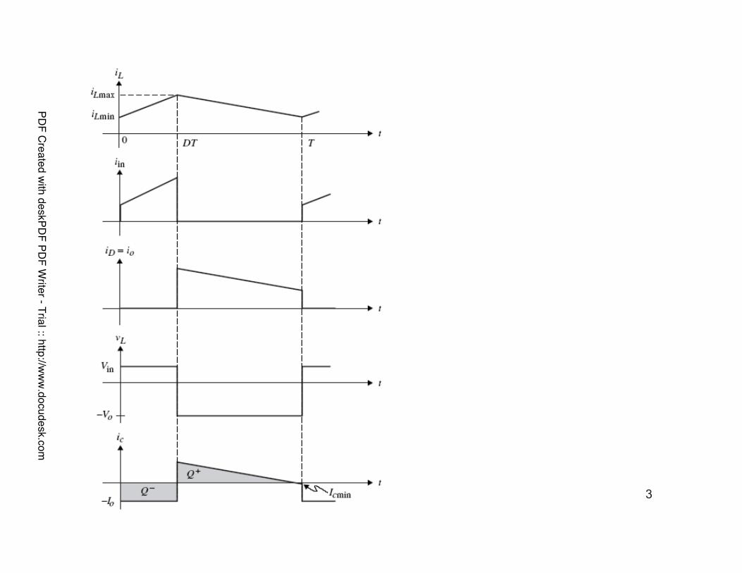
CCM Buck-Boost Output voltage ripple
Use capacitor charge
o
oc
c
o
Q DTI
DTVV
CR
V D
V RCf
! "
! "
!"
find vc(t)?
PDF C
reated with deskPD
F PDF W
riter - Trial :: http://ww
w.docudesk.com

8
DCM Buck-Boost ConverterMode 1: S on
Mode 2: S off Mode 3: S & D off
Mode 1:
Mode 2:
0 ! DT
DT ! D1T
D1T ! TMode 3: ( ) 0 ( )L c oi t i t I! ! "
Switch and diode voltage stress= Vin + Vo
PDF C
reated with deskPD
F PDF W
riter - Trial :: http://ww
w.docudesk.com

9
( )L
VinI DT DT
L!
1 1( ) 0 ( ) ( )L L
VoI D T D D T I DT
L
"! ! " #
from mode 1
from mode 2
Using the above two equations, or using volt-second balance
1( ) 0Vin DT Vo D D T" " !
1
Vo D
Vin D D!
"
PDF C
reated with deskPD
F PDF W
riter - Trial :: http://ww
w.docudesk.com
10
11
,
1I ( ) ( )
( )12I2
L
D avg o
DT D D TVinD D D TVo
IR T L
! " "# # # #
1( ) (1)2
Vo RD D D T
Vin L# "
1
1
1
1
( )
(1 )
1( 1) (2)
DM
D D
D D M D
D M D M
D DM
#"
" #
# $
# $
Solve for M
Substitute eq.2 in eq.1
2 n
DM
%#
n
L
RT%& '#( )
* +
PDF C
reated with deskPD
F PDF W
riter - Trial :: http://ww
w.docudesk.com

11
DCM Buck-Boost output voltage ripple
max max
1 1
max 11
max
( )
( )( )
L L o
L o
L
I I I
D D T t DT
I I D D Tt DT
I
!"
! !
! !! "
1 max
2max 1
max
1( )( )
2
( ) ( )1
2
L o
L oc
L
Q t DT I I
I I D D TV
C I
# " ! !
! !# "
maxIL
VinDT
L"
Triangles similarity
1
1( 1)D DM
" $
ic
Io
ILmax
Io
t1
t
vc
Vo
PDF C
reated with deskPD
F PDF W
riter - Trial :: http://ww
w.docudesk.com
Buck Converter Analysis: iPES Examples for Buck DCM
DC/DC-Converter Basic Topologies Buck-Converter - (1) Buck-Converter - (2) Buck-Converter - (3)
Buck-Converter: Start-Up with Constant Duty Cycle

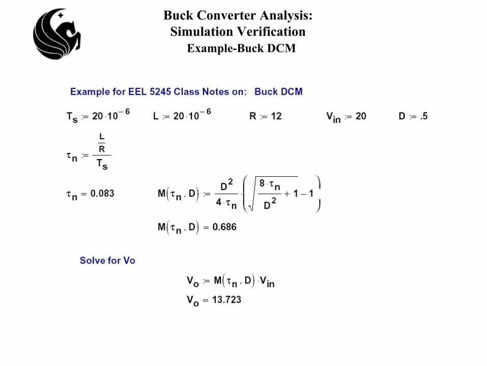
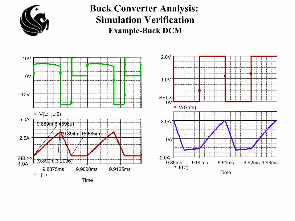
Buck Converter Analysis: Simulation Verification
Example-Buck DCM
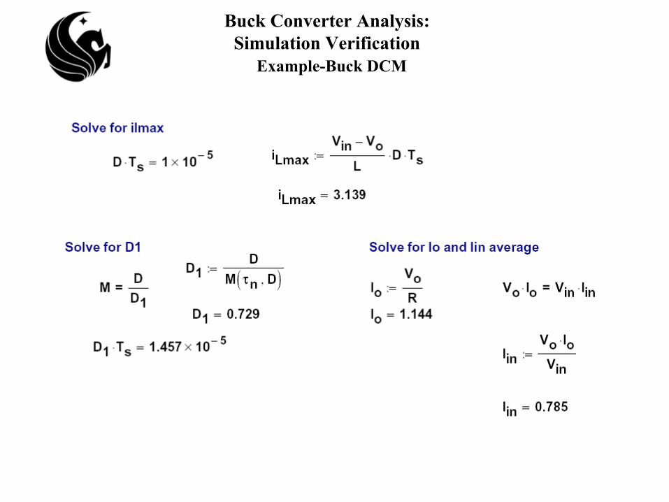
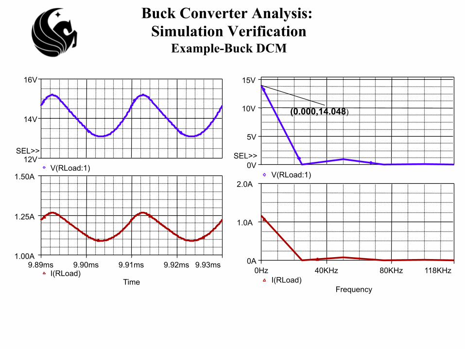
Buck Converter Analysis: Simulation Verification
Example-Buck DCM
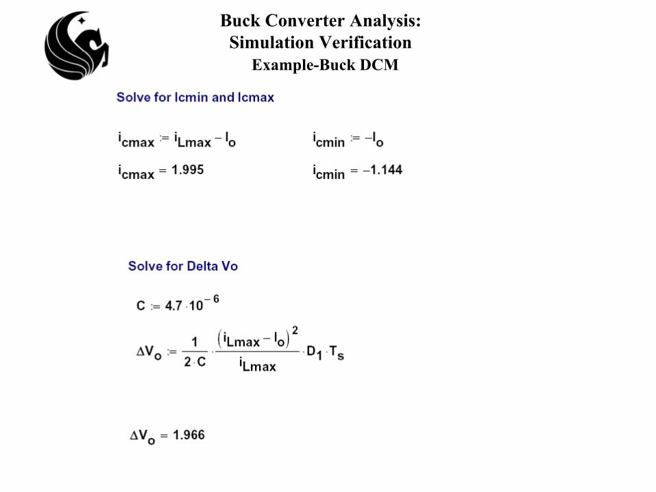
Buck Converter Analysis: Simulation Verification
Example-Buck DCM
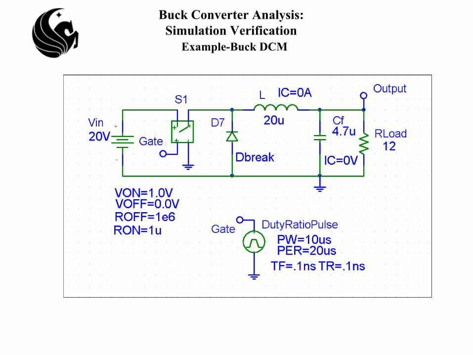
Buck Converter Analysis: Simulation Verification
Example-Buck DCM
Buck Converter Analysis: Simulation Verification
Example-Buck DCM
Buck Converter Analysis: Simulation Verification
Example-Buck DCM
Time 9.8875ms 9.9000ms 9.9125ms
I(L)
2.5A
5.0A
-1.0A SEL>>
(9.894m,15.685m)
(9.890m,3.2006)
9.880m,6.4896u) V(L:1,L:2)
-10V
0V
10V
Time 9.89ms 9.90ms 9.91ms 9.92ms 9.93ms
I(Cf) -2.0A
0A
2.0A V(Gate) 0V
1.0V
2.0V
SEL>>
Buck Converter Analysis: Simulation Verification
Example-Buck DCM
Time 9.89ms 9.90ms 9.91ms 9.92ms 9.93ms
I(RLoad) 1.00A
1.25A
1.50A V(RLoad:1) 12V
14V
16V
SEL>>
Frequency 0Hz 40KHz 80KHz 118KHz
I(RLoad) 0A
1.0A
2.0A V(RLoad:1) 0V
5V
10V
15V
SEL>>
(0.000,14.048)
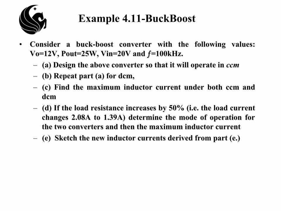
Example 4.11-BuckBoost
• Consider a buck-boost converter with the following values: Vo=12V, Pout=25W, Vin=20V and ƒ=100kHz. – (a) Design the above converter so that it will operate in ccm – (b) Repeat part (a) for dcm, – (c) Find the maximum inductor current under both ccm and
dcm – (d) If the load resistance increases by 50% (i.e. the load current
changes 2.08A to 1.39A) determine the mode of operation for the two converters and then the maximum inductor current
– (e) Sketch the new inductor currents derived from part (e.)

Example 4.11-BuckBoost
Note-This is an arbitrary assignment that puts us into CCM mode. Since in CCM M is independent of L, we do not effect the conversion ratio so long as L>Lcrit. The value of L chosen does effect ripple current in the inductor though.
Vo 12:= Vin 20:= Po 25:= f 100 103⋅:=
Ts1f
:=
(a) For CCM
1220
D1 D−
solve D,
float 3,.375→
RVo
2
Po:=
D .375:=R 5.76=
Ts 1 10 5−×=
Lcrit R Ts⋅1 D−( )2
2⋅:= D Ts⋅ 3.75 10 6−×=
Lcrit 1.125 10 5−×=
Chose L higher than Lcrit for CCM
L .1 10 3−⋅:=

Example 4.11-BuckBoost
(b) For DCM Chose L to less than Lcrit L 5 10 6−⋅:=
MD
2 τn⋅τn
LR
Ts:=
τn 0.087= D1220
2 τn⋅⋅:=
D 0.25=
MD
D1 D−solve D1,
23
→

Example 4.11-BuckBoost
L .1 10 3−⋅:= D .375:=(c) For CCM
iLmaxD Vin⋅
R 1 D−( )2⋅
Vin D⋅ Ts⋅
2 L⋅+:= iLmin
D Vin⋅
R 1 D−( )2⋅
Vin D⋅ Ts⋅
2 L⋅−:=
iLmax 3.708= iLmin 2.958=
(c) For DCM L 5 10 6−⋅:= D .25:=
iLmaxVinL
D⋅ Ts⋅:=
iLmax 10=
Example 4.11-BuckBoost
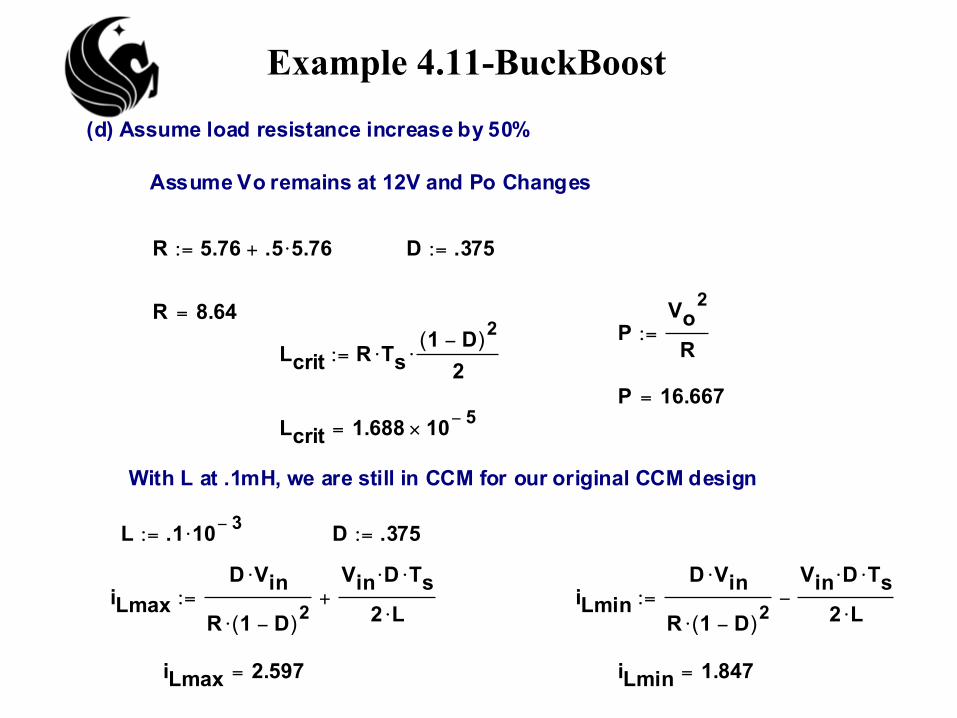
(d) Assume load resistance increase by 50%
Assume Vo remains at 12V and Po Changes
R 5.76 .5 5.76⋅+:= D .375:=
R 8.64=P
Vo2
R:=
Lcrit R Ts⋅1 D−( )2
2⋅:=
P 16.667=
Lcrit 1.688 10 5−×=
With L at .1mH, we are still in CCM for our original CCM design
L .1 10 3−⋅:= D .375:=
iLmaxD Vin⋅
R 1 D−( )2⋅
Vin D⋅ Ts⋅
2 L⋅+:= iLmin
D Vin⋅
R 1 D−( )2⋅
Vin D⋅ Ts⋅
2 L⋅−:=
iLmax 2.597= iLmin 1.847=
Example 4.11-BuckBoost
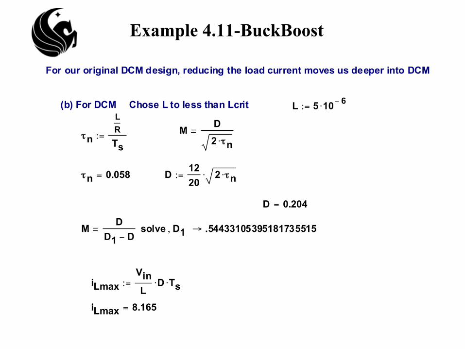
For our original DCM design, reducing the load current moves us deeper into DCM
(b) For DCM Chose L to less than Lcrit L 5 10 6−⋅:=
MD
2 τn⋅τn
LR
Ts:=
τn 0.058= D1220
2 τn⋅⋅:=
D 0.204=
MD
D1 D−solve D1, .54433105395181735515→
iLmaxVinL
D⋅ Ts⋅:=
iLmax 8.165=
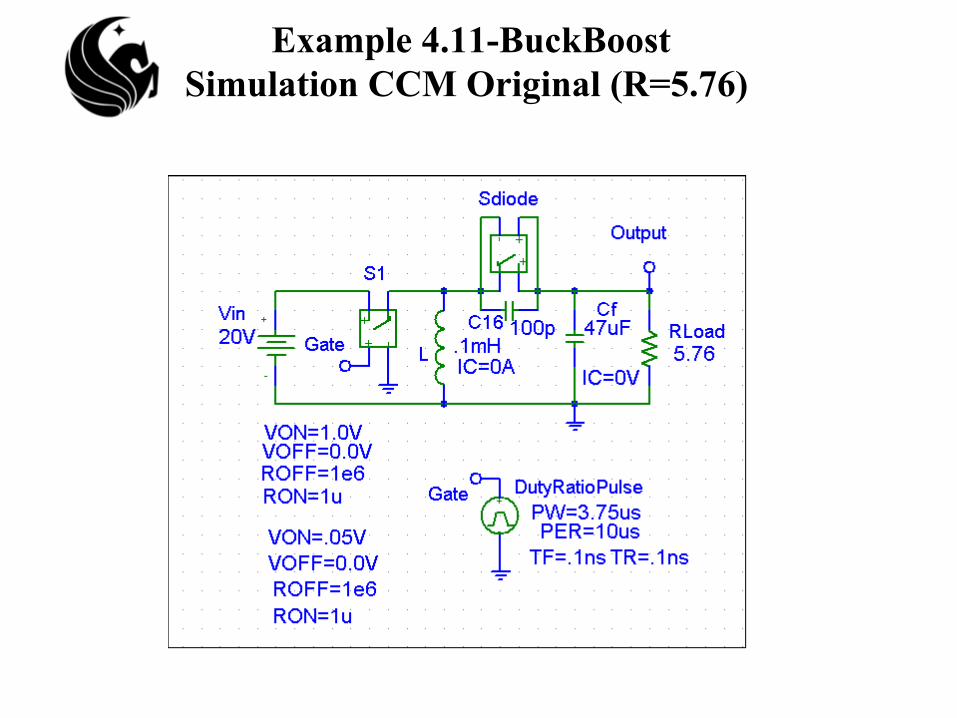
Example 4.11-BuckBoost Simulation CCM Original (R=5.76)

Example 4.11-BuckBoost Simulation CCM Original (R=5.76)
Time 0s 5ms 10ms 15ms
V(Output) -20V
-15V
-10V
-5V
0V
Time 14.980ms 14.985ms 14.990ms 14.995ms
-I(L) 2.8A
3.2A
3.6A
4.0A
Time 14.980ms 14.985ms 14.990ms 14.995ms
V(Gate) -I(L) 0
1.0
2.0
3.0
4.0
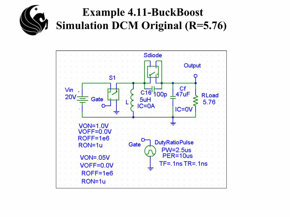
Example 4.11-BuckBoost Simulation DCM Original (R=5.76)

Example 4.11-BuckBoost Simulation DCM Original (R=5.76)
Time 14.980ms 14.985ms 14.990ms 14.995ms
-I(L) V(Gate) -4
0
4
8
12
Time 0s 5ms 10ms 15ms
V(Output) -15V
-10V
-5V
0V

Example 4.11-BuckBoost Simulation CCM New (R=8.64)
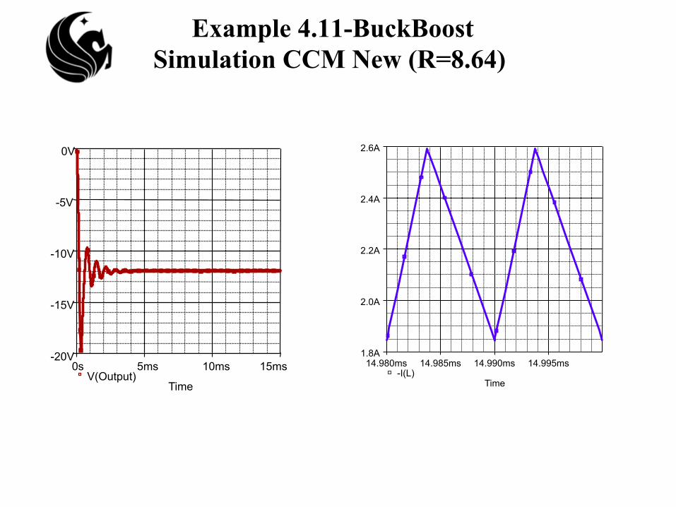
Example 4.11-BuckBoost Simulation CCM New (R=8.64)
Time 0s 5ms 10ms 15ms
V(Output) -20V
-15V
-10V
-5V
0V
Time 14.980ms 14.985ms 14.990ms 14.995ms
-I(L) 1.8A
2.0A
2.2A
2.4A
2.6A

Example 4.11-BuckBoost Simulation DCM New (R=8.64)
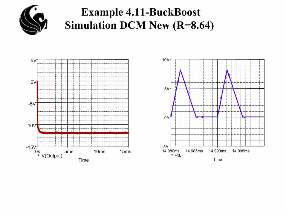
Example 4.11-BuckBoost Simulation DCM New (R=8.64)
Time 14.980ms 14.985ms 14.990ms 14.995ms
-I(L) -5A
0A
5A
10A
Time 0s 5ms 10ms 15ms
V(Output) -15V
-10V
-5V
0V
5V