eecs150 - digital design lecture 14 - project description ...cs150/sp10/lecture/lec14-proj3.pdf ·...
TRANSCRIPT
Spring 2010 EECS150 - Lec14-proj3 Page
EECS150 - Digital DesignLecture 14 - Project Description,
Part 3
March 4, 2010John Wawrzynek
1
Spring 2010 EECS150 - Lec14-proj3 Page
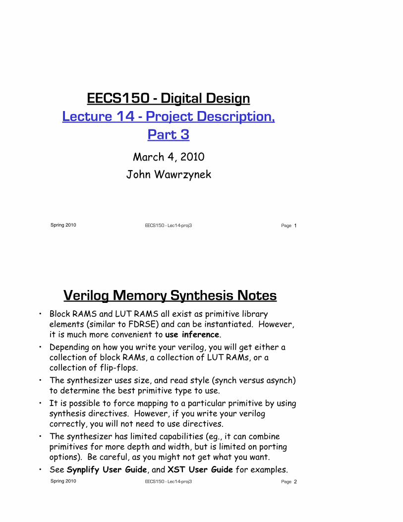
Verilog Memory Synthesis Notes• Block RAMS and LUT RAMS all exist as primitive library
elements (similar to FDRSE) and can be instantiated. However, it is much more convenient to use inference.
• Depending on how you write your verilog, you will get either a collection of block RAMs, a collection of LUT RAMs, or a collection of flip-flops.
• The synthesizer uses size, and read style (synch versus asynch) to determine the best primitive type to use.
• It is possible to force mapping to a particular primitive by using synthesis directives. However, if you write your verilog correctly, you will not need to use directives.
• The synthesizer has limited capabilities (eg., it can combine primitives for more depth and width, but is limited on porting options). Be careful, as you might not get what you want.
• See Synplify User Guide, and XST User Guide for examples.2
Spring 2010 EECS150 - Lec14-proj3 Page
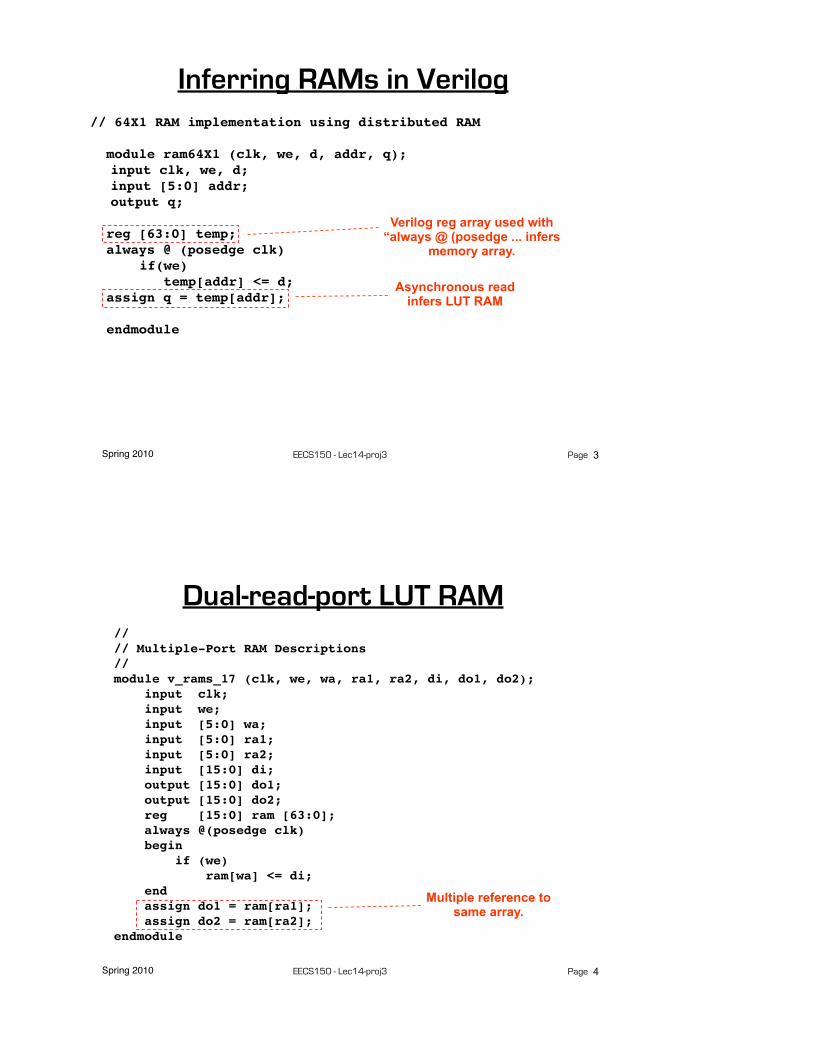
Inferring RAMs in Verilog
3
// 64X1 RAM implementation using distributed RAM
module ram64X1 (clk, we, d, addr, q);input clk, we, d;input [5:0] addr;output q;
reg [63:0] temp; always @ (posedge clk)
if(we) temp[addr] <= d;
assign q = temp[addr];
endmodule
Asynchronous read infers LUT RAM
Verilog reg array used with “always @ (posedge ... infers
memory array.
Spring 2010 EECS150 - Lec14-proj3 Page
Dual-read-port LUT RAM
4
// // Multiple-Port RAM Descriptions // module v_rams_17 (clk, we, wa, ra1, ra2, di, do1, do2); input clk; input we; input [5:0] wa; input [5:0] ra1; input [5:0] ra2; input [15:0] di; output [15:0] do1; output [15:0] do2; reg [15:0] ram [63:0]; always @(posedge clk) begin if (we) ram[wa] <= di; end assign do1 = ram[ra1]; assign do2 = ram[ra2]; endmodule
Multiple reference to same array.

Spring 2010 EECS150 - Lec14-proj3 Page
Block RAM Inference
5
// // Single-Port RAM with Synchronous Read // module v_rams_07 (clk, we, a, di, do); input clk; input we; input [5:0] a; input [15:0] di; output [15:0] do; reg [15:0] ram [63:0]; reg [5:0] read_a; always @(posedge clk) begin if (we) ram[a] <= di; read_a <= a; end assign do = ram[read_a]; endmodule
Synchronous read (registered read address)
infers Block RAM
Spring 2010 EECS150 - Lec14-proj3 Page
Block RAM initialization
6
module RAMB4_S4 (data_out, ADDR, data_in, CLK, WE); output[3:0] data_out; input [2:0] ADDR; input [3:0] data_in; input CLK, WE; reg [3:0] mem [7:0]; reg [3:0] read_addr;
initial begin $readmemb("data.dat", mem); end always@(posedge CLK) read_addr <= ADDR;
assign data_out = mem[read_addr];
always @(posedge CLK) if (WE) mem[ADDR] = data_in;
endmodule
“data.dat” contains initial RAM contents, it gets put into the bitfile and loaded at configuration time. (Remake bits to change contents)
Spring 2010 EECS150 - Lec14-proj3 Page
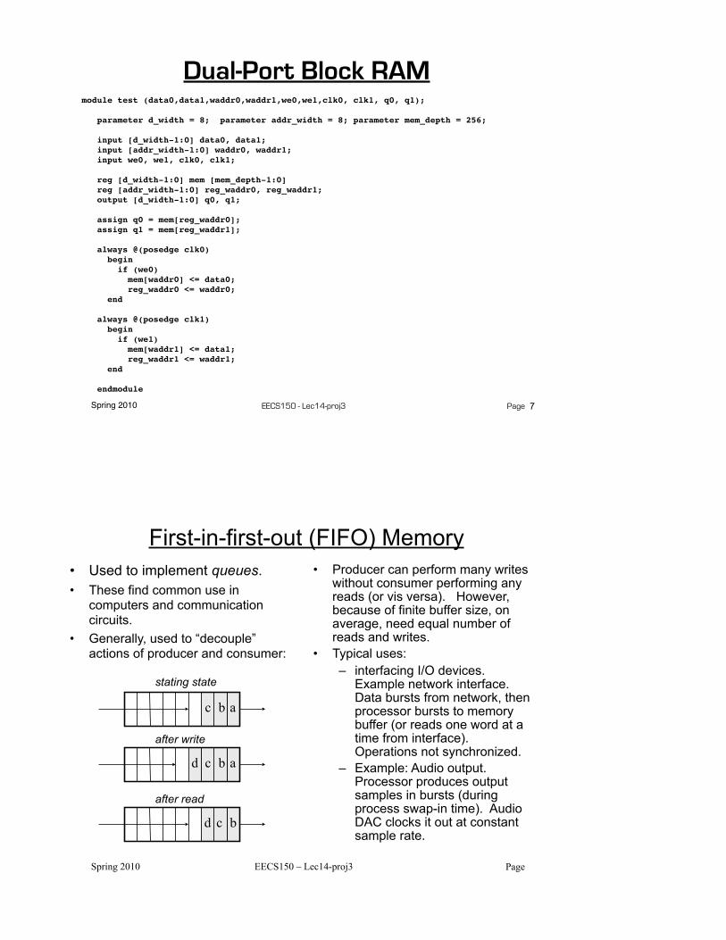
Dual-Port Block RAM
7
module test (data0,data1,waddr0,waddr1,we0,we1,clk0, clk1, q0, q1);
parameter d_width = 8; parameter addr_width = 8; parameter mem_depth = 256;
input [d_width-1:0] data0, data1; input [addr_width-1:0] waddr0, waddr1; input we0, we1, clk0, clk1;
reg [d_width-1:0] mem [mem_depth-1:0] reg [addr_width-1:0] reg_waddr0, reg_waddr1; output [d_width-1:0] q0, q1;
assign q0 = mem[reg_waddr0]; assign q1 = mem[reg_waddr1];
always @(posedge clk0) begin if (we0) mem[waddr0] <= data0; reg_waddr0 <= waddr0; end
always @(posedge clk1) begin if (we1) mem[waddr1] <= data1; reg_waddr1 <= waddr1; end
endmodule
Spring 2010 EECS150 – Lec14-proj3 Page
First-in-first-out (FIFO) Memory• Used to implement queues. • These find common use in
computers and communication circuits.
• Generally, used to “decouple” actions of producer and consumer:
• Producer can perform many writes without consumer performing any reads (or vis versa). However, because of finite buffer size, on average, need equal number of reads and writes.
• Typical uses: – interfacing I/O devices.
Example network interface. Data bursts from network, then processor bursts to memory buffer (or reads one word at a time from interface). Operations not synchronized.
– Example: Audio output. Processor produces output samples in bursts (during process swap-in time). Audio DAC clocks it out at constant sample rate.
stating state
after write
after read
abc
abcd
bcd

Spring 2010 EECS150 – Lec14-proj3 Page
FIFO Interfaces
• After write or read operation, FULL and EMPTY indicate status of buffer.
• Used by external logic to control own reading from or writing to the buffer.
• FIFO resets to EMPTY state.• HALF FULL (or other indicator of
partial fullness) is optional.
• Address pointers are used internally to keep next write position and next read position into a dual-port memory.
• If pointers equal after write ⇒ FULL:
• If pointers equal after read ⇒ EMPTY:
DIN
DOUT
WE
REEMPTY
FULLHALF FULL
RST CLK
FIFOwrite ptr
read ptr
write ptr read ptr
write ptr read ptr
Spring 2010 EECS150 – Lec14-proj3 Page
FIFO Implementation Details
WE RE equal EMPTYi FULLi
0 0 0 0 0 0 0 1 EMPTYi-1 FULLi-1
0 1 0 0 0 0 1 1 1 0 1 0 0 0 0 1 0 1 0 1 1 1 0 0 0 1 1 1 EMPTYi-1 FULLi-1
• Assume, dual-port memory with asynchronous read, synchronous write.
• Binary counter for each of read and write address. CEs (count enable) controlled by WE and RE.
• Equal comparator to see when pointers match.• Flip-flop each for FULL and EMPTY flags: • Control logic (FSM) with
truth-table shown to left.

Spring 2010 EECS150 – Lec14-proj3 Page
Xilinx Virtex5 FIFOs• Virtex5 BlockRAMS include dedicated circuits for FIFOs.• Details in User Guide (ug190).• Takes advantage of separate dual ports and independent ports
clocks.
Spring 2010 EECS150 - Lec14-proj3 Page
Processor Design Considerations (1/2)• Register File: Consider distributed RAM (LUT RAM)
– Size is close to what is needed: distributed RAM primitive configurations are 32 or 64 bits deep. Extra width is easily achieved by parallel arrangements.
– LUT-RAM configurations offer multi-porting options - useful for register files.
– Asynchronous read, might be useful by providing flexibility on where to put register read in the pipeline.
• Instruction / Data Memories : Consider Block RAM– Higher density, lower cost for large number of bits– A single 36kbit Block RAM implements 1K 32-bit words.– Configuration stream based initialization, permits a simple “boot
strap” procedure.
• Other Memories in Project? Ethernet? Video?12
Spring 2010 EECS150 - Lec14-proj3 Page
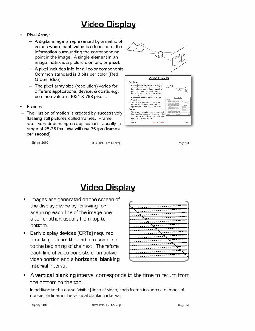
Video Display• Pixel Array:
– A digital image is represented by a matrix of values where each value is a function of the information surrounding the corresponding point in the image. A single element in an image matrix is a picture element, or pixel.
– A pixel includes info for all color components. Common standard is 8 bits per color (Red, Green, Blue)
– The pixel array size (resolution) varies for different applications, device, & costs, e.g. common value is 1024 X 768 pixels.
13
• Frames: – The illusion of motion is created by successively
flashing still pictures called frames. Frame rates vary depending on application. Usually in range of 25-75 fps. We will use 75 fps (frames per second).
Spring 2010 EECS150 - Lec14-proj3 Page
Video Display
14
• A vertical blanking interval corresponds to the time to return from the bottom to the top.
– In addition to the active (visible) lines of video, each frame includes a number of non-visible lines in the vertical blanking interval.
• Images are generated on the screen of the display device by “drawing” or scanning each line of the image one after another, usually from top to bottom.
• Early display devices (CRTs) required time to get from the end of a scan line to the beginning of the next. Therefore each line of video consists of an active video portion and a horizontal blanking interval interval.
Spring 2010 EECS150 - Lec14-proj3 Page
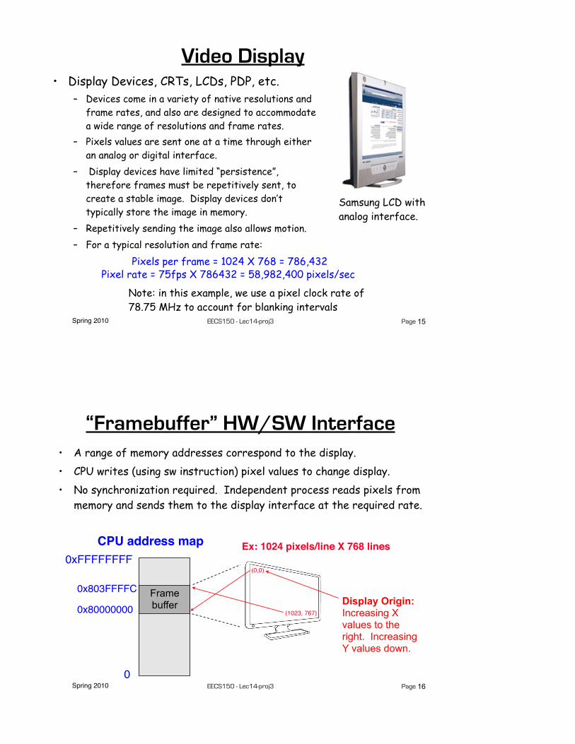
Video Display• Display Devices, CRTs, LCDs, PDP, etc.
– Devices come in a variety of native resolutions and frame rates, and also are designed to accommodate a wide range of resolutions and frame rates.
– Pixels values are sent one at a time through either an analog or digital interface.
– Display devices have limited “persistence”, therefore frames must be repetitively sent, to create a stable image. Display devices don’t typically store the image in memory.
– Repetitively sending the image also allows motion.– For a typical resolution and frame rate:
15
Pixel rate = 75fps X 786432 = 58,982,400 pixels/secPixels per frame = 1024 X 768 = 786,432
Note: in this example, we use a pixel clock rate of 78.75 MHz to account for blanking intervals
Samsung LCD with analog interface.
Spring 2010 EECS150 - Lec14-proj3 Page
“Framebuffer” HW/SW Interface• A range of memory addresses correspond to the display.• CPU writes (using sw instruction) pixel values to change display.• No synchronization required. Independent process reads pixels from
memory and sends them to the display interface at the required rate.
0
0xFFFFFFFFCPU address map
16
Ex: 1024 pixels/line X 768 lines
0x80000000
0x803FFFFC Frame buffer Display Origin:
Increasing X values to the right. Increasing Y values down.
(0,0)
(1023, 767)
Spring 2010 EECS150 - Lec14-proj3 Page
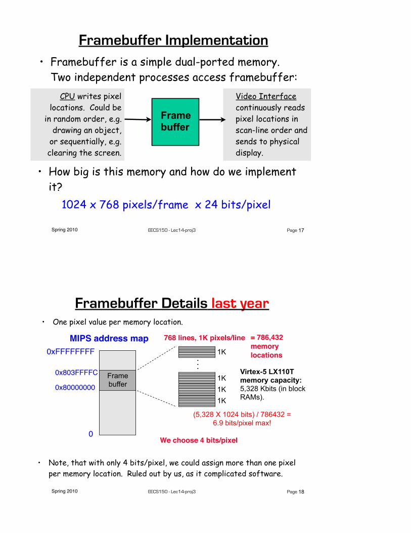
Framebuffer Implementation• Framebuffer is a simple dual-ported memory.
Two independent processes access framebuffer:
17
CPU writes pixel locations. Could be
in random order, e.g. drawing an object,
or sequentially, e.g. clearing the screen.
Video Interface continuously reads pixel locations in scan-line order and sends to physical display.
• How big is this memory and how do we implement it? 1024 x 768 pixels/frame x 24 bits/pixel
Framebuffer
Spring 2010 EECS150 - Lec14-proj3 Page
Framebuffer Details last year• One pixel value per memory location.
18
Virtex-5 LX110T memory capacity: 5,328 Kbits (in block RAMs).
0
0xFFFFFFFFMIPS address map 768 lines, 1K pixels/line
0x80000000
0x803FFFFC Frame buffer
1K1K1K
1K...
• Note, that with only 4 bits/pixel, we could assign more than one pixel per memory location. Ruled out by us, as it complicated software.
= 786,432 memory locations
(5,328 X 1024 bits) / 786432 = 6.9 bits/pixel max!
We choose 4 bits/pixel

Spring 2010 EECS150 - Lec14-proj3 Page
Color Map
19
4 bits per pixel, allows software to assign each screen location, one of 16 different colors.
However, physical display interface uses 8 bits / pixel-color. Therefore entire pallet is 224 colors.
Color map is memory mapped to CPU address space, so software can set the color table. Addresses: 0x8040_0000 0x8040_003C, one 24-bit entry per memory address.
R G BR G BR G B
R G B...
24 bits
16 entries
pixel value from framebuffer
pixel color to video interface
Color Map converts 4 bit pixel values to 24 bit colors.
Spring 2010 EECS150 - Lec14-proj3 Page
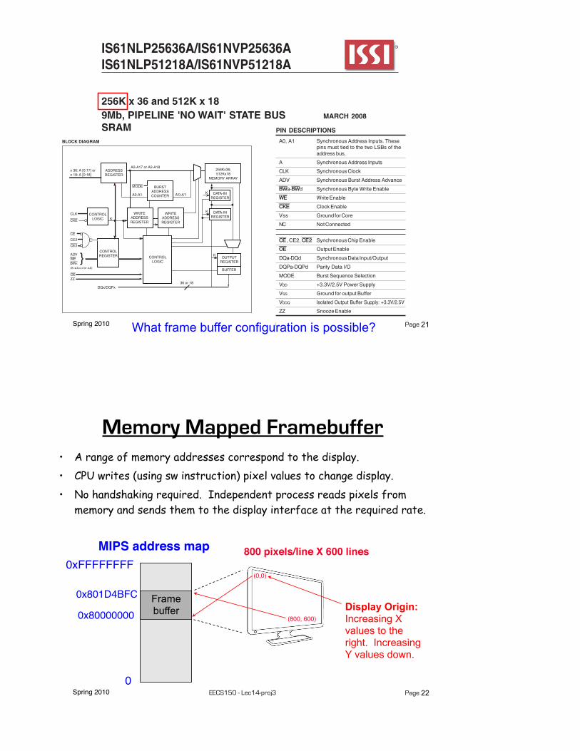
XUP Board External SRAM
20
More generally, how does software interface to I/O devices?
*ZBT (ZBT stands for zero bus turnaround) — the turnaround is the number of clock cycles it takes to change access to the SRAM from write to read and vice versa. The turnaround for ZBT SRAMs or the latency between read and write cycle is zero.
“ZBT” synchronous SRAM, 9 Mb on 32-bit data bus, with four “parity” bits256K x 36 bits(located under the removable LCD)
Spring 2010 EECS150 - Lec14-proj3 Page 21
Integrated Silicon Solution, Inc. — www.issi.com — 1-800-379-4774 1Rev. F03/27/08
IS61NLP25636A/IS61NVP25636AIS61NLP51218A/IS61NVP51218A
Copyright © 2006 Integrated Silicon Solution, Inc. All rights reserved. ISSI reserves the right to make changes to this specification and its products at any time without notice. ISSI assumes no liabilityarising out of the application or use of any information, products or services described herein. Customers are advised to obtain the latest version of this device specification before relying on anypublished information and before placing orders for products.
FEATURES
• 100 percent bus utilization
• No wait cycles between Read and Write
• Internal self-timed write cycle
• Individual Byte Write Control
• Single R/W (Read/Write) control pin
• Clock controlled, registered address,data and control
• Interleaved or linear burst sequence control usingMODE input
• Three chip enables for simple depth expansionand address pipelining
• Power Down mode
• Common data inputs and data outputs
• CKE pin to enable clock and suspend operation
• JEDEC 100-pin TQFP, 165-ball PBGA and 119-ball PBGA packages
• Power supply:NVP: VDD 2.5V (± 5%), VDDQ 2.5V (± 5%)NLP: VDD 3.3V (± 5%), VDDQ 3.3V/2.5V (± 5%)
• JTAG Boundary Scan for PBGA packages
• Industrial temperature available
• Lead-free available
DESCRIPTION
The 9 Meg 'NLP/NVP' product family feature high-speed,low-power synchronous static RAMs designed to providea burstable, high-performance, 'no wait' state, device fornetworking and communications applications. They areorganized as 256K words by 36 bits and 512K words by 18bits, fabricated with ISSI's advanced CMOS technology.
Incorporating a 'no wait' state feature, wait cycles areeliminated when the bus switches from read to write, orwrite to read. This device integrates a 2-bit burst counter,high-speed SRAM core, and high-drive capability outputsinto a single monolithic circuit.
All synchronous inputs pass through registers are controlledby a positive-edge-triggered single clock input. Operationsmay be suspended and all synchronous inputs ignoredwhen Clock Enable, CKE is HIGH. In this state the internaldevice will hold their previous values.
All Read, Write and Deselect cycles are initiated by theADV input. When the ADV is HIGH the internal burstcounter is incremented. New external addresses can beloaded when ADV is LOW.
Write cycles are internally self-timed and are initiated bythe rising edge of the clock inputs and when WE is LOW.Separate byte enables allow individual bytes to be written.
A burst mode pin (MODE) defines the order of the burstsequence. When tied HIGH, the interleaved burst sequenceis selected. When tied LOW, the linear burst sequence isselected.
256K x 36 and 512K x 189Mb, PIPELINE 'NO WAIT' STATE BUSSRAM
MARCH 2008
FAST ACCESS TIME
Symbol Parameter -250 -200 UnitstKQ Clock Access Time 2.6 3.1 nstKC Cycle Time 4 5 ns
Frequency 250 200 MHz
8 Integrated Silicon Solution, Inc. — www.issi.com — 1-800-379-4774Rev. F
03/27/08
IS61NLP25636A/IS61NVP25636AIS61NLP51218A/IS61NVP51218A
PIN CONFIGURATION100-Pin TQFP
512K x 18
123456789101112131415161718192021222324252627282930
807978777675747372717069686766656463626160595857565554535251
100 99 98 97 96 95 94 93 92 91 90 89 88 87 86 85 84 83 82 81
31 32 33 34 35 36 37 38 39 40 41 42 43 44 45 46 47 48 49 50
A
NC
NC
VDDQ
Vss
NCDQPa
DQa
DQa
Vss
VDDQ
DQa
DQaVssNCVDD
ZZ
DQa
DQa
VDDQ
Vss
DQa
DQa
NCNC
Vss
VDDQ
NCNCNC
NC
NC
NC
VDDQ
Vss
NCNC
DQb
DQb
Vss
VDDQ
DQb
DQbNC
VDD
NCVss
DQb
DQb
VDDQ
VssDQb
DQb
DQPbNC
Vss
VDDQ
NCNCNC
A A CE
CE
2
NC
NCBWb
BWa
CE2
VD
D
Vss
CLKWE
CKE
OE
AD
VN
C
A A A
MO
DE A A A A A1
A0
NC
NC
Vss
VD
D
NC
NC A A A A A A A
123456789101112131415161718192021222324252627282930
807978777675747372717069686766656463626160595857565554535251
100 99 98 97 96 95 94 93 92 91 90 89 88 87 86 85 84 83 82 81
31 32 33 34 35 36 37 38 39 40 41 42 43 44 45 46 47 48 49 50
DQPb
DQb
DQb
VDDQ
Vss
DQbDQb
DQb
DQb
Vss
VDDQ
DQb
DQbVssNCVDD
ZZ
DQa
DQa
VDDQ
Vss
DQa
DQa
DQaDQaVss
VDDQ
DQaDQaDQPa
DQPc
DQc
DQc
VDDQ
Vss
DQcDQc
DQc
DQc
Vss
VDDQ
DQc
DQcNC
VDD
NC
Vss
DQd
DQd
VDDQ
VssDQd
DQd
DQdDQdVss
VDDQ
DQdDQd
DQPd
A
A CE
CE
2
BWd
BWc
BWb
BWa
CE2
VD
D
Vss
CLKWE
CKE
OE
AD
VN
C
A A A
MO
DE A A A A A1
A0
NC
NC
Vss
VD
D
NC
NC A A A A A A A
256K x 36
PIN DESCRIPTIONS
A0, A1 Synchronous Address Inputs. Thesepins must tied to the two LSBs of theaddress bus.
A Synchronous Address Inputs
CLK Synchronous Clock
ADV Synchronous Burst Address Advance
BWa-BWd Synchronous Byte Write Enable
WE Write Enable
CKE Clock Enable
Vss Ground for Core
NC Not Connected
CE, CE2, CE2 Synchronous Chip Enable
OE Output Enable
DQa-DQd Synchronous Data Input/Output
DQPa-DQPd Parity Data I/O
MODE Burst Sequence Selection
VDD +3.3V/2.5V Power Supply
VSS Ground for output Buffer
VDDQ Isolated Output Buffer Supply: +3.3V/2.5V
ZZ Snooze Enable
2 Integrated Silicon Solution, Inc. — www.issi.com — 1-800-379-4774Rev. F
03/27/08
IS61NLP25636A/IS61NVP25636AIS61NLP51218A/IS61NVP51218A
BLOCK DIAGRAM
ADVWE }BWŸX(X=a,b,c,d or a,b)
CE
CE2
CE2
CONTROLLOGIC
256Kx36;512Kx18
MEMORY ARRAY
WRITEADDRESSREGISTER
WRITEADDRESSREGISTER
CONTROLLOGIC
OUTPUTREGISTER
BUFFER
ADDRESSREGISTER
x 36: A [0:17] orx 18: A [0:18]
CLK
CKE
A2-A17 or A2-A18
A0-A1 A'0-A'1
BURSTADDRESSCOUNTER
MODE
DATA-INREGISTER
DATA-INREGISTER
CONTROLREGISTER
OEZZ
36 or 18
K
K
DQx/DQPx
K
K
What frame buffer configuration is possible?
Spring 2010 EECS150 - Lec14-proj3 Page
Memory Mapped Framebuffer• A range of memory addresses correspond to the display.• CPU writes (using sw instruction) pixel values to change display.• No handshaking required. Independent process reads pixels from
memory and sends them to the display interface at the required rate.
0
0xFFFFFFFFMIPS address map
22
800 pixels/line X 600 lines
0x80000000
0x801D4BFC Frame buffer Display Origin:
Increasing X values to the right. Increasing Y values down.
(0,0)
(800, 600)

Spring 2010 EECS150 - Lec14-proj3 Page
Framebuffer Details• One pixel value per memory location.
23
XUP SRAM memory capacity: ~8 Mbits (in external SRAMs).
0
0xFFFFFFFFMIPS address map 600 lines, 800 pixels/line
0x80000000
0x801D4BFC Frame buffer
800800800
800...
• Note, that we assign only one 16 bit pixel per memory location.• Two pixel address map to one address in the SRAM (it is 32bits wide).
= 480,000 memory locations
8Mbits / 480000 = 17.5 bits/pixel max!
We choose 16 bits/pixel{ Red[4:0] ; Green[5:0] ; Blue[4:0] }
Spring 2010 EECS150 - Lec14-proj3 Page
MIPS150 Video Subsystem
24
• Gives software ability to display information on screen.• Equivalent to standard graphics cards:
• Processor can directly write the display bit map• 2D Graphics acceleration

Spring 2010 EECS150 - Lec14-proj3 Page
Physical Video Interface
25
DVI connector:accommodates analog and digital formats
DVI Transmitter Chip, Chrontel 7301C.
Implements standard signaling voltage levels for video monitors. Digital to analog conversion for analog display formats.
Spring 2010 EECS150 - Lec14-proj3 Page
Video Interface
26
More generally, how does software interface to I/O devices?
Video Interface Block: accepts pixel values from FB, streams pixels values and control signals to physical device.
Frame Buffer: provides a memory mapped programming interface to video display.
You do!
We do!
CPU
VideoInterface
Frame Buffer
FPGA