eecs 373 lab 3: introduction to memory mapped i/o 373 lab 3: introduction to memory mapped i/o in...
TRANSCRIPT
EECS 373 Lab 3: Introduction to Memory Mapped I/O
In this lab we will learn:
To develop custom peripheral hardware in the SmartFusion FPGA using the Libero CAD tools.
The fundamentals of memory-mapped I/O (MMIO).
To interface the ARM peripheral bus (APB3) to registers created in the FPGA.
1.0 Overview
If you recall from Lab 2, we used the GPIO by writing a register location with assembler instructions. We treated the IO as though it is a memory location. To write the GPIO register you used the following assembler instructions:
.equ GPIO_OUT_BASE, 0x40013000
movw r0, #:lower16:GPIO_OUT_BASE
movt r0, #:upper16:GPIO_OUT_BASE
str r1, [r0, #0]
In effect, you are witting a memory location (or register) at 0x4001300 where some bit of the register at that location are connected to the LED in hardware.
ARM Peripheral BUS (APB3)
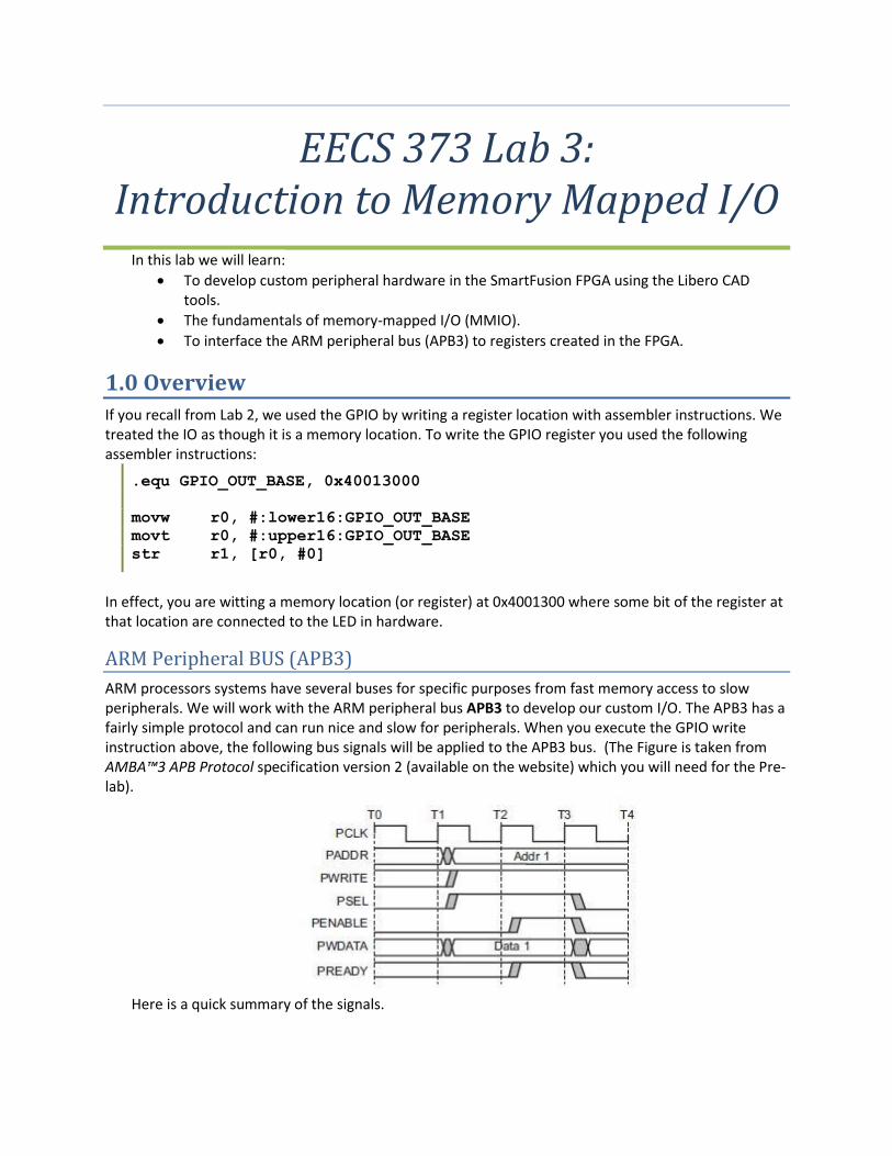
ARM processors systems have several buses for specific purposes from fast memory access to slow peripherals. We will work with the ARM peripheral bus APB3 to develop our custom I/O. The APB3 has a fairly simple protocol and can run nice and slow for peripherals. When you execute the GPIO write instruction above, the following bus signals will be applied to the APB3 bus. (The Figure is taken from AMBA™3 APB Protocol specification version 2 (available on the website) which you will need for the Pre-lab).
Here is a quick summary of the signals.
PCLK, Peripheral Bus Clock Provided by the bus master or ARM processor in this case. The APB3 is a synchronous bus with all timing and operations executed relative to the clock. The clock period can be set by the user via Libero tools.
PADDR, Peripheral Address. Provided by the bus master (Cortex M3 processor). The address is a subset of I/O address. For the GPIO write example, it is a subset of the address 0x40013000.
PWRITE, Peripheral Write. Provided by the bus master (Cortex M3 processor). Indicates if the transaction is a write or a read. Write and reads are from the perspective of the bus master. For our purposes, the bus master will always be the processor.
PSEL, Peripheral Select. Provided by user logic. A select signal decoded from the peripheral address. For the GPIO write example, it is the address 0x4001300.
PENABLE, Peripheral Enable. Provided by the bus master (Cortex M3 processor). This signal indicates an access phase. The peripheral should be ready and it can be used to signal the peripheral.
PWDATA, Peripheral Write Data Bus. Provided by the bus master (Cortex M3 processor). This is the data bus connection between the processor and peripheral.
PREADY, Peripheral Ready Provided by the peripheral. This is used to signal the processor that the peripheral is ready and the cycle can be completed. The GPIO register of lab 2 has additional logic to automatically generate a PREADY signal.
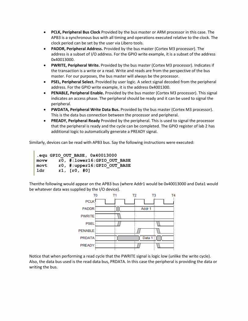
Similarly, devices can be read with APB3 bus. Say the following instructions were executed:
.equ GPIO_OUT_BASE, 0x40013000
movw r0, #:lower16:GPIO_OUT_BASE
movt r0, #:upper16:GPIO_OUT_BASE
ldr r1, [r0, #0]
Thenthe following would appear on the APB3 bus (where Addr1 would be 0x40013000 and Data1 would be whatever data was supplied by the I/O device).
Notice that when performing a read cycle that the PWRITE signal is logic low (unlike the write cycle). Also, the data bus used is the read data bus, PRDATA. In this case the peripheral is providing the data or writing the bus.
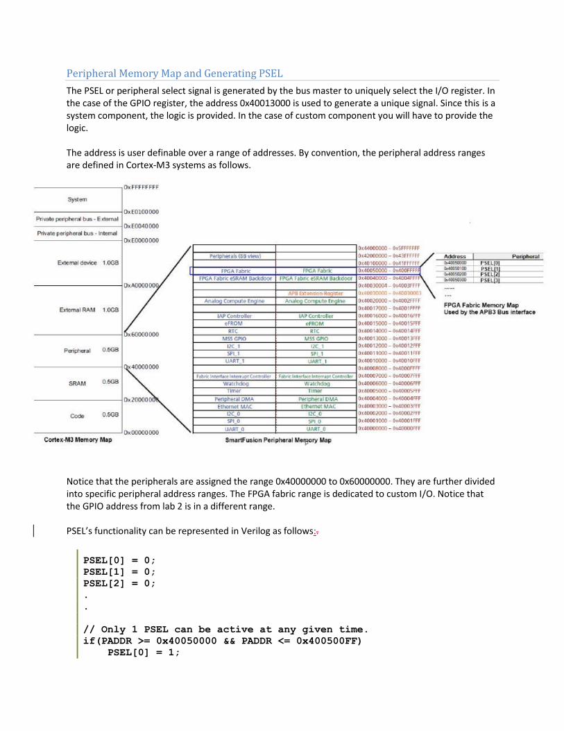
Peripheral Memory Map and Generating PSEL
The PSEL or peripheral select signal is generated by the bus master to uniquely select the I/O register. In the case of the GPIO register, the address 0x40013000 is used to generate a unique signal. Since this is a system component, the logic is provided. In the case of custom component you will have to provide the logic. The address is user definable over a range of addresses. By convention, the peripheral address ranges are defined in Cortex-M3 systems as follows.
Notice that the peripherals are assigned the range 0x40000000 to 0x60000000. They are further divided into specific peripheral address ranges. The FPGA fabric range is dedicated to custom I/O. Notice that the GPIO address from lab 2 is in a different range. PSEL’s functionality can be represented in Verilog as follows:.
PSEL[0] = 0;
PSEL[1] = 0;
PSEL[2] = 0;
.
.
// Only 1 PSEL can be active at any given time.
if(PADDR >= 0x40050000 && PADDR <= 0x400500FF)
PSEL[0] = 1;
else if(PADDR >= 0x40050100 && PADDR <= 0x400501FF)
PSEL[1] = 1;
else if(PADDR >= 0x40050200 && PADDR <= 0x400502FF)
PSEL[2] = 1;
else
.
.
.
You will NOT have to write this Verilog. It will be generated for you with Libero library logic. Notice that the PSELs for this case are generated over a range of 0x100 byte addresses. This range is provided to allow for more than one register to be addressed and associated with one PSEL. From an application point of view, you might have a peripheral that has more than one register. It could be something as simple as having a number of LEDs each with their own address or something as complex as a serial-bus controller, hard-drive controller or Ethernet card. From the Verilog, you can see that PSEL represents the decode of bits 31 through 8 or the left most 6 digits 0x40050000. The last two digits or addresses [7:0] are used to byte, half word or word address the range between PSELs. For example, to select the word register at 0x4005000A you can do something equivalent to the following conditional: If (PSEL && PADDR[7:0] == 0x0A) rather than If (PADDR[31:0] == 0x4005000A). If you attempt to use constants larger than 8 bits as in the last case, you will mismatch the PADDR port size resulting in a subtle synthesis issue that will prevent your decoder from working.
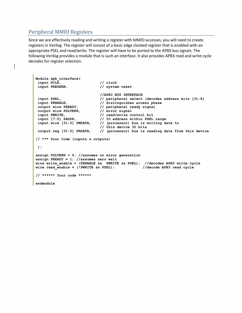
Peripheral MMIO Registers
Since we are effectively reading and writing a register with MMIO accesses, you will need to create registers in Verilog. The register will consist of a basic edge clocked register that is enabled with an appropriate PSEL and read/write. The register will have to be ported to the APB3 bus signals. The following Verilog provides a module that is such an interface. It also provides APB3 read and write cycle decodes for register selection.
Module apb_interface(
input PCLK, // clock
input PRESERN, // system reset
//APB3 BUS INTERFACE
input PSEL, // peripheral select (decodes address bits [31:8]
input PENABLE, // distinguishes access phase
output wire PREADY, // peripheral ready signal
output wire PSLVERR, // error signal
input PWRITE, // read/write control bit
input [7:0] PADDR, // IO address within PSEL range
input wire [31:0] PWDATA, // (processor) bus is writing data to
// this device 32 bits
output reg [31:0] PRDATA, // (processor) bus is reading data from this device
// *** Your Code (inputs & outputs)
);
assign PSLVERR = 0; //assumes no error generation
assign PREADY = 1; //assumes zero wait
wire write_enable = (PENABLE && PWRITE && PSEL); //decodes APB3 write cycle
wire read_enable = (!PWRITE && PSEL); //decode APB3 read cycle
// ****** Your code ******
endmodule
2.0 Pre-lab
This pre-lab covers material you’ll need in the in-lab. This includes the basics of the APB protocol (which was covered above), working with MMIO in assembly and C and building a modulo-10,000,000 counter that will be needed for the in-lab.Pre-labs are done individually! Make sure you make a copy of this prelab before you turn it in as you will need it during the lab!
Basics of the ARM APB Protocol
In lecture, you have seen timing diagrams for both read and write transactions on the Advanced Peripheral Bus (APB). Additional details can be found in the AMBA™3 APB Protocol specification (available on the website).
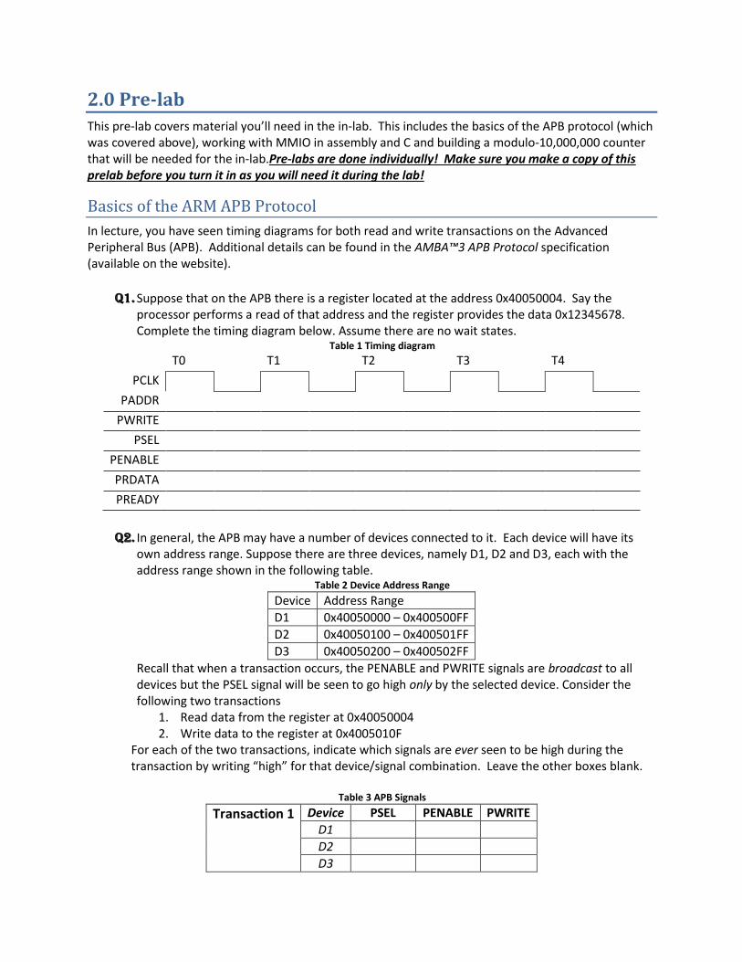
Q1. Suppose that on the APB there is a register located at the address 0x40050004. Say the processor performs a read of that address and the register provides the data 0x12345678. Complete the timing diagram below. Assume there are no wait states.
Table 1 Timing diagram
T0 T1 T2 T3 T4
PCLK
PADDR
PWRITE
PSEL
PENABLE
PRDATA
PREADY
Q2. In general, the APB may have a number of devices connected to it. Each device will have its own address range. Suppose there are three devices, namely D1, D2 and D3, each with the address range shown in the following table.
Table 2 Device Address Range
Device Address Range
D1 0x40050000 – 0x400500FF
D2 0x40050100 – 0x400501FF
D3 0x40050200 – 0x400502FF
Recall that when a transaction occurs, the PENABLE and PWRITE signals are broadcast to all devices but the PSEL signal will be seen to go high only by the selected device. Consider the following two transactions
1. Read data from the register at 0x40050004 2. Write data to the register at 0x4005010F
For each of the two transactions, indicate which signals are ever seen to be high during the transaction by writing “high” for that device/signal combination. Leave the other boxes blank.
Table 3 APB Signals
Transaction 1 Device PSEL PENABLE PWRITE
D1
D2
D3
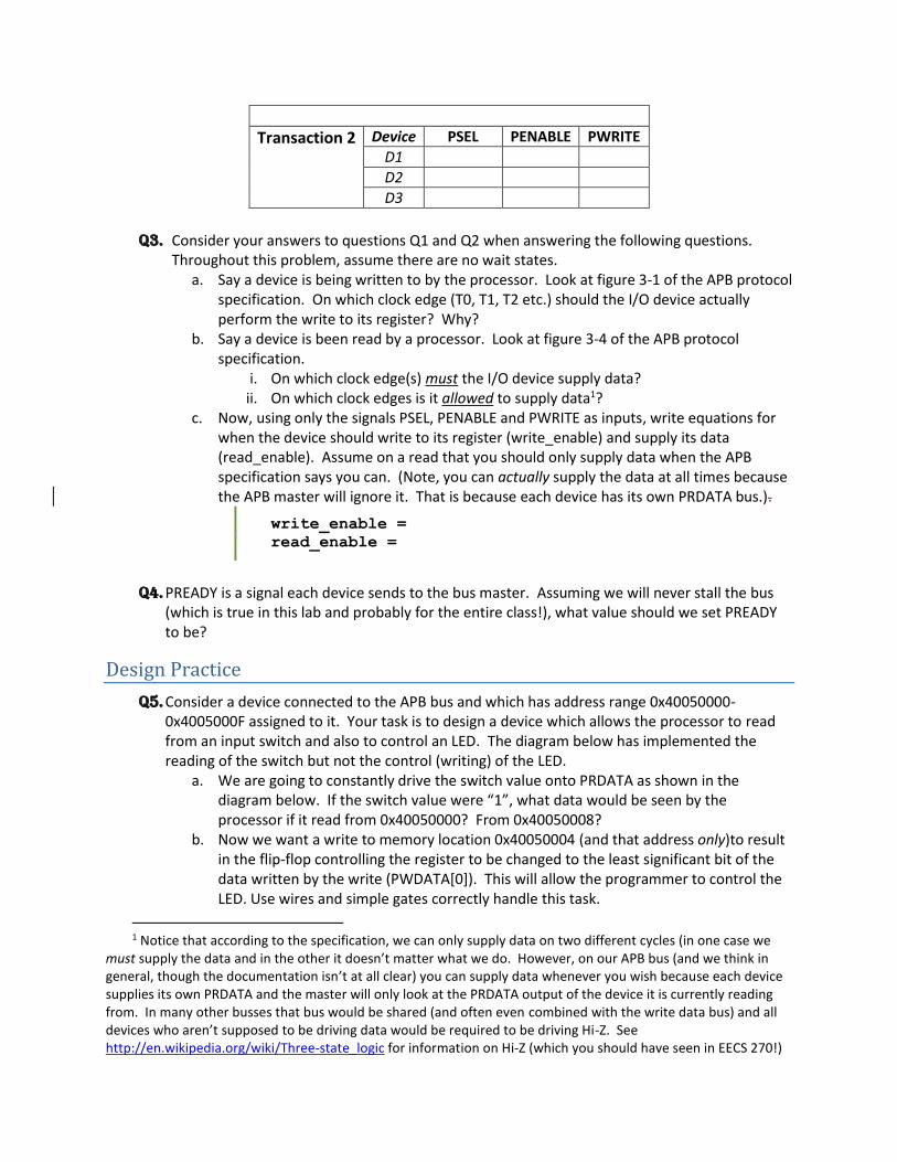
Transaction 2 Device PSEL PENABLE PWRITE
D1
D2
D3
Q3. Consider your answers to questions Q1 and Q2 when answering the following questions. Throughout this problem, assume there are no wait states.
a. Say a device is being written to by the processor. Look at figure 3-1 of the APB protocol specification. On which clock edge (T0, T1, T2 etc.) should the I/O device actually perform the write to its register? Why?
b. Say a device is been read by a processor. Look at figure 3-4 of the APB protocol specification.
i. On which clock edge(s) must the I/O device supply data? ii. On which clock edges is it allowed to supply data1?
c. Now, using only the signals PSEL, PENABLE and PWRITE as inputs, write equations for when the device should write to its register (write_enable) and supply its data (read_enable). Assume on a read that you should only supply data when the APB specification says you can. (Note, you can actually supply the data at all times because the APB master will ignore it. That is because each device has its own PRDATA bus.).
write_enable =
read_enable =
Q4. PREADY is a signal each device sends to the bus master. Assuming we will never stall the bus (which is true in this lab and probably for the entire class!), what value should we set PREADY to be?
Design Practice
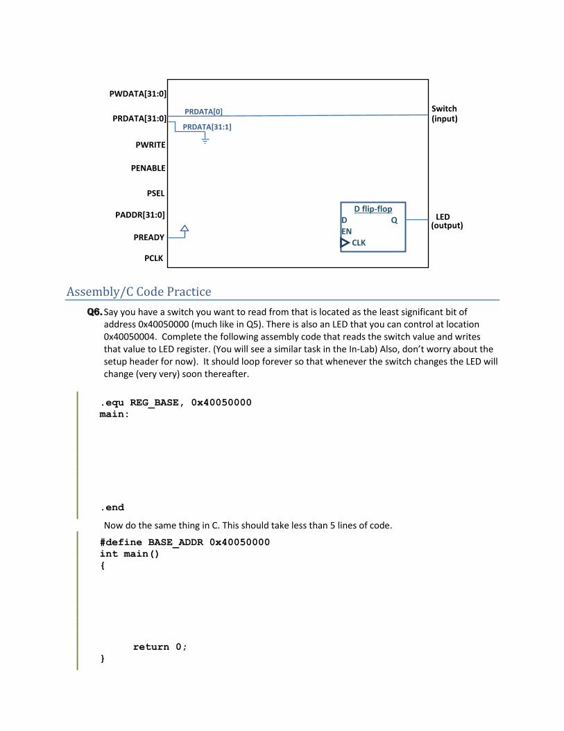
Q5. Consider a device connected to the APB bus and which has address range 0x40050000-0x4005000F assigned to it. Your task is to design a device which allows the processor to read from an input switch and also to control an LED. The diagram below has implemented the reading of the switch but not the control (writing) of the LED.
a. We are going to constantly drive the switch value onto PRDATA as shown in the diagram below. If the switch value were “1”, what data would be seen by the processor if it read from 0x40050000? From 0x40050008?
b. Now we want a write to memory location 0x40050004 (and that address only)to result in the flip-flop controlling the register to be changed to the least significant bit of the data written by the write (PWDATA[0]). This will allow the programmer to control the LED. Use wires and simple gates correctly handle this task.
1 Notice that according to the specification, we can only supply data on two different cycles (in one case we
must supply the data and in the other it doesn’t matter what we do. However, on our APB bus (and we think in general, though the documentation isn’t at all clear) you can supply data whenever you wish because each device supplies its own PRDATA and the master will only look at the PRDATA output of the device it is currently reading from. In many other busses that bus would be shared (and often even combined with the write data bus) and all devices who aren’t supposed to be driving data would be required to be driving Hi-Z. See http://en.wikipedia.org/wiki/Three-state_logic for information on Hi-Z (which you should have seen in EECS 270!)
Assembly/C Code Practice
Q6. Say you have a switch you want to read from that is located as the least significant bit of address 0x40050000 (much like in Q5). There is also an LED that you can control at location 0x40050004. Complete the following assembly code that reads the switch value and writes that value to LED register. (You will see a similar task in the In-Lab) Also, don’t worry about the setup header for now). It should loop forever so that whenever the switch changes the LED will change (very very) soon thereafter.
.equ REG_BASE, 0x40050000
main:
.end
Now do the same thing in C. This should take less than 5 lines of code.
#define BASE_ADDR 0x40050000
int main()
{
return 0;
}
PRDATA[31:0]
PWRITE
PENABLE
PSEL
PADDR[31:0]
PREADY
Switch (input)
LED (output)
PWDATA[31:0]
PRDATA[0]
PRDATA[31:1]
D flip-flop
D Q
EN
CLK
PCLK
Timers and servos
Q7. Create a 32-bit modulo-100,000,000 up-counter in Verilog. (That is, each clock tick the counter will increment until it reaches 99,999,999. The clock tick after it reaches that value the counter goes to 0 and continues to count from there each time wrapping around to 0 to 99,999,999.) You will be using a similar counter for your in-lab.
//32 bit down counter with a counter register
reg [31:0] counter;
always @(posedge PCLK) //PCLK is the system clock input
begin
if(counter >________)
counter<=________;
else
counter<=________;
end
Read part 4 of the in-lab, http://en.wikipedia.org/wiki/Pulse-width_modulation and http://www.servodatabase.com/servo/hitec/hs-422.
Q8. . Draw a figure and write a paragraph that explains how a servo is controlled.
3.0 In-lab
The In-lab is broken into four parts. Part 1 is highly directed. In it you will create the hardware and software needed to do a trivial I/O task—reading a switch and driving an LED. In part 2, you will learn how to observe the APB transactions on our oscilloscope. In part 3, you will expand the software from part 1. And finally, in part 4, you will create a servo controller largely from scratch. Answers to questions asked during the In-Lab must be submitted with the post lab.
Part1: Using one switch to control the LED
In this section, you will follow the tutorial to build a module that can read the value of a switch, and write that value to the LED.
1. Create a Libero project Create a project named “lab3p1”, and use the following settings: Go to the Libero Tutorial you did earlier to for settings.
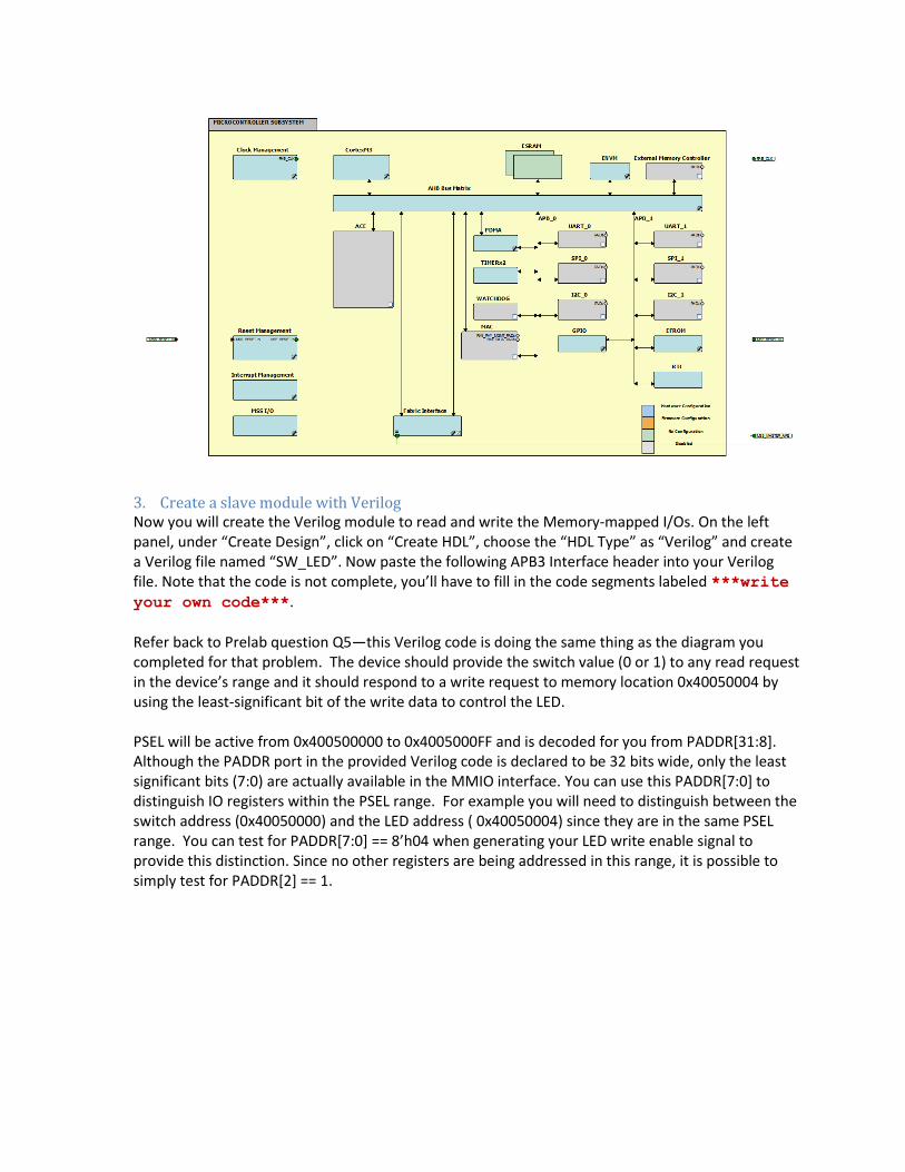
2. Setup the Micro-controller SubSystem (MSS) In this case, we want the SmartFusion to be responsible for controlling the APB3. Therefore, we need to set it up as the master. To do so, open up the MSS and double-click the Fabric Interface block. In this block, set the Interface Type to AMBA APB3, and tick the Use Master Interface checkbox. Close this dialog. Make sure the Fabric Interface block is checked, and every other block is unchecked. Next, enable FAB_CLK in Clock Management. Also, enable Enable Chip-level Reset and Enable MSS To Fabric Reset in Reset Management. After all of this is done, your MSS should look exactly like the photo below. Save and generate.
3. Create a slave module with Verilog Now you will create the Verilog module to read and write the Memory-mapped I/Os. On the left panel, under “Create Design”, click on “Create HDL”, choose the “HDL Type” as “Verilog” and create a Verilog file named “SW_LED”. Now paste the following APB3 Interface header into your Verilog file. Note that the code is not complete, you’ll have to fill in the code segments labeled ***write your own code***.
Refer back to Prelab question Q5—this Verilog code is doing the same thing as the diagram you completed for that problem. The device should provide the switch value (0 or 1) to any read request in the device’s range and it should respond to a write request to memory location 0x40050004 by using the least-significant bit of the write data to control the LED. PSEL will be active from 0x400500000 to 0x4005000FF and is decoded for you from PADDR[31:8]. Although the PADDR port in the provided Verilog code is declared to be 32 bits wide, only the least significant bits (7:0) are actually available in the MMIO interface. You can use this PADDR[7:0] to distinguish IO registers within the PSEL range. For example you will need to distinguish between the switch address (0x40050000) and the LED address ( 0x40050004) since they are in the same PSEL range. You can test for PADDR[7:0] == 8’h04 when generating your LED write enable signal to provide this distinction. Since no other registers are being addressed in this range, it is possible to simply test for PADDR[2] == 1.
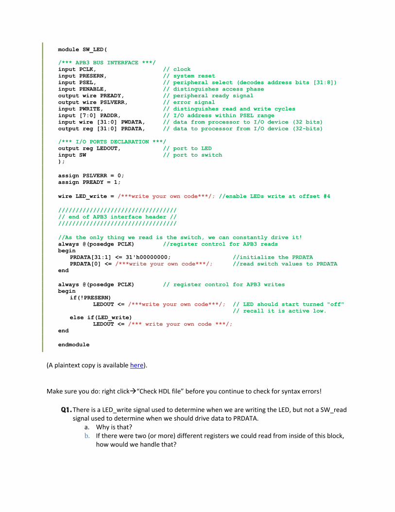
module SW_LED(
/*** APB3 BUS INTERFACE ***/ input PCLK, // clock input PRESERN, // system reset input PSEL, // peripheral select (decodes address bits [31:8]) input PENABLE, // distinguishes access phase output wire PREADY, // peripheral ready signal output wire PSLVERR, // error signal input PWRITE, // distinguishes read and write cycles input [7:0] PADDR, // I/O address within PSEL range input wire [31:0] PWDATA, // data from processor to I/O device (32 bits) output reg [31:0] PRDATA, // data to processor from I/O device (32-bits)
/*** I/O PORTS DECLARATION ***/ output reg LEDOUT, // port to LED input SW // port to switch );
assign PSLVERR = 0; assign PREADY = 1;
wire LED_write = /***write your own code***/; //enable LEDs write at offset #4
////////////////////////////////// // end of APB3 interface header // //////////////////////////////////
//As the only thing we read is the switch, we can constantly drive it! always @(posedge PCLK) //register control for APB3 reads begin PRDATA[31:1] <= 31'h00000000; //initialize the PRDATA PRDATA[0] <= /***write your own code***/; //read switch values to PRDATA end
always @(posedge PCLK) // register control for APB3 writes begin if(!PRESERN) LEDOUT <= /***write your own code***/; // LED should start turned "off"
// recall it is active low. else if(LED_write) LEDOUT <= /*** write your own code ***/; end
endmodule
(A plaintext copy is available here). Make sure you do: right click“Check HDL file” before you continue to check for syntax errors!
Q1. There is a LED_write signal used to determine when we are writing the LED, but not a SW_read signal used to determine when we should drive data to PRDATA.
a. Why is that? b. If there were two (or more) different registers we could read from inside of this block,
how would we handle that?
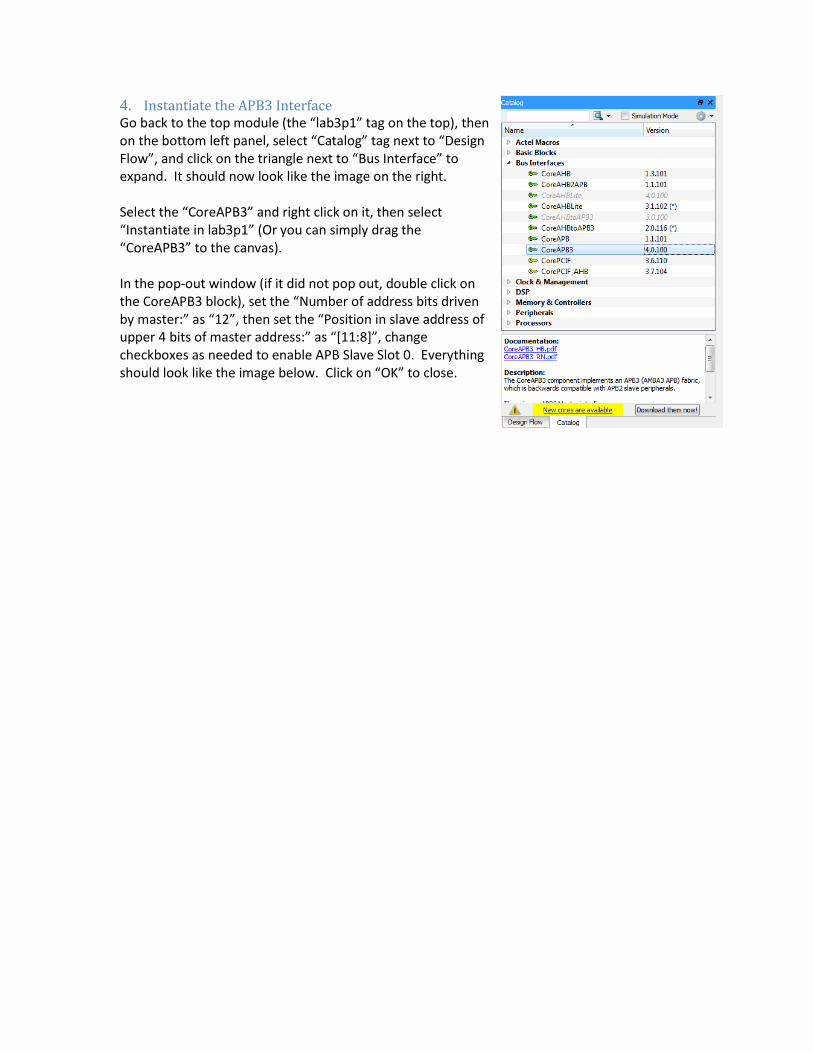
4. Instantiate the APB3 Interface Go back to the top module (the “lab3p1” tag on the top), then on the bottom left panel, select “Catalog” tag next to “Design Flow”, and click on the triangle next to “Bus Interface” to expand. It should now look like the image on the right.
Select the “CoreAPB3” and right click on it, then select “Instantiate in lab3p1” (Or you can simply drag the “CoreAPB3” to the canvas).
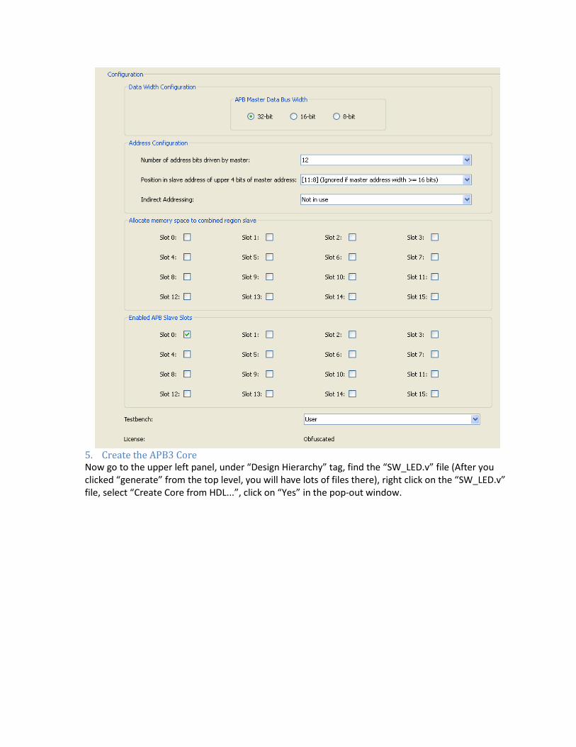
In the pop-out window (if it did not pop out, double click on the CoreAPB3 block), set the “Number of address bits driven by master:” as “12”, then set the “Position in slave address of upper 4 bits of master address:” as “[11:8]”, change checkboxes as needed to enable APB Slave Slot 0. Everything should look like the image below. Click on “OK” to close.
5. Create the APB3 Core Now go to the upper left panel, under “Design Hierarchy” tag, find the “SW_LED.v” file (After you clicked “generate” from the top level, you will have lots of files there), right click on the “SW_LED.v” file, select “Create Core from HDL...”, click on “Yes” in the pop-out window.
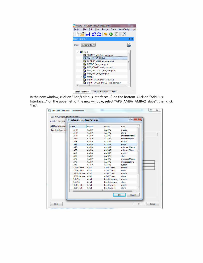
In the new window, click on “Add/Edit bus interfaces...” on the bottom. Click on “Add Bus Interface...” on the upper left of the new window, select “APB_AMBA_AMBA2_slave”, then click “OK”.
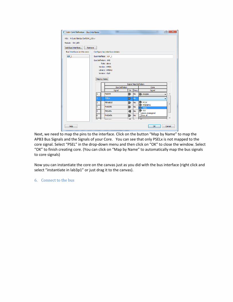
Next, we need to map the pins to the interface. Click on the button “Map by Name” to map the APB3 Bus Signals and the Signals of your Core. You can see that only PSELx is not mapped to the core signal. Select “PSEL” in the drop-down menu and then click on “OK” to close the window. Select “OK” to finish creating core. (You can click on “Map by Name” to automatically map the bus signals to core signals)
Now you can instantiate the core on the canvas just as you did with the bus interface (right click and select “instantiate in lab3p1” or just drag it to the canvas). 6. Connect to the bus
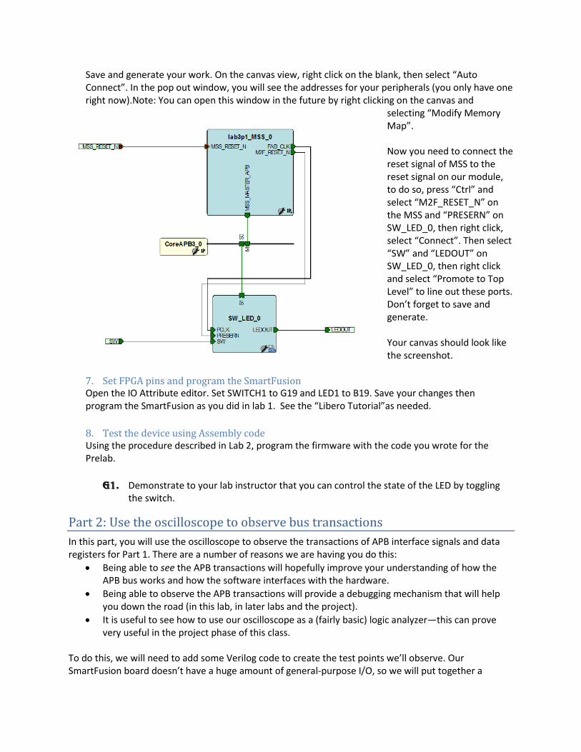
Save and generate your work. On the canvas view, right click on the blank, then select “Auto Connect”. In the pop out window, you will see the addresses for your peripherals (you only have one right now).Note: You can open this window in the future by right clicking on the canvas and
selecting “Modify Memory Map”. Now you need to connect the reset signal of MSS to the reset signal on our module, to do so, press “Ctrl” and select “M2F_RESET_N” on the MSS and “PRESERN” on SW_LED_0, then right click, select “Connect”. Then select “SW” and “LEDOUT” on SW_LED_0, then right click and select “Promote to Top Level” to line out these ports. Don’t forget to save and generate.
Your canvas should look like the screenshot.
7. Set FPGA pins and program the SmartFusion Open the IO Attribute editor. Set SWITCH1 to G19 and LED1 to B19. Save your changes then program the SmartFusion as you did in lab 1. See the “Libero Tutorial”as needed.
8. Test the device using Assembly code Using the procedure described in Lab 2, program the firmware with the code you wrote for the Prelab.
G1. Demonstrate to your lab instructor that you can control the state of the LED by toggling the switch.
Part 2: Use the oscilloscope to observe bus transactions
In this part, you will use the oscilloscope to observe the transactions of APB interface signals and data registers for Part 1. There are a number of reasons we are having you do this:
Being able to see the APB transactions will hopefully improve your understanding of how the APB bus works and how the software interfaces with the hardware.
Being able to observe the APB transactions will provide a debugging mechanism that will help you down the road (in this lab, in later labs and the project).
It is useful to see how to use our oscilloscope as a (fairly basic) logic analyzer—this can prove very useful in the project phase of this class.
To do this, we will need to add some Verilog code to create the test points we’ll observe. Our SmartFusion board doesn’t have a huge amount of general-purpose I/O, so we will put together a
number of different pins in different places to get all the information we want. First, in SW_LED.v, add this line in your module header to instantiate a 16-bit output wire named test. We will observe these test points later with our oscilloscope.
output wire [15:0] test
Now add the following lines below the module header.
assign test[15] = PCLK;
assign test[14:12] = PADDR[4:2];
assign test[11] = PSEL;
assign test[10] = PENABLE;
assign test[9] = PREADY;
assign test[8] = PWRITE;
assign test[7:0] = PWRITE ? PWDATA : PRDATA;
Next, in your top level canvas, right click on your SW_LED module and choose “Update Instances with Latest Component”. You will see the output wire “test”. Promote test to top. Open “Create/Edit I/O Attributes” and assign the pins according to the table below:
Now you will connect the SmartFusion to the Logic Analyzer on the oscilloscope through the Probe Cable.
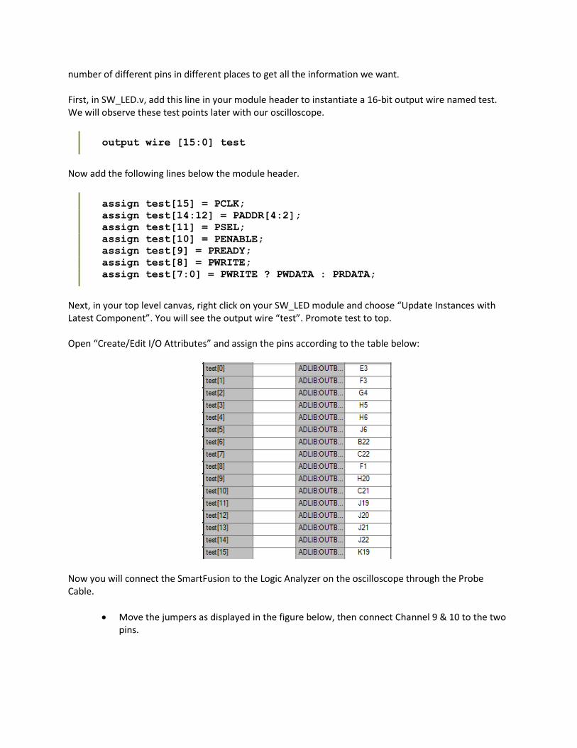
Move the jumpers as displayed in the figure below, then connect Channel 9 & 10 to the two pins.
10 9
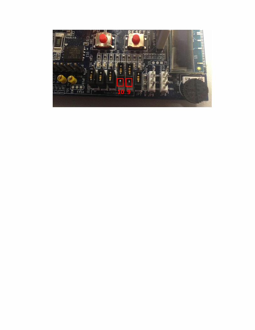
Connect Channels 0-8 to F0 through F8 on the extension board and connect Channels 11-15 to the User I/O. When you are done, the connections should be the same as the figure below.
Connect the cable to digital connector on the bottom of the oscilloscope. Then, to set up the oscilloscope, push “Default Setup”, then “Digital”. Also, we aren’t using either of the analog signals, so disable them by pushing the numbered button associated with the signal.
15……11
8………0
10 9
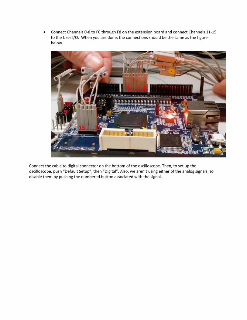
Now we are going to create a data bus. Press the button that corresponds to the option “Bus” on the
screen (you may have to push “Digital” again). Once you do that, you will go to the following screen. Make sure you enable a bus (either BUS1 or BUS2 is fine). The box next to BUS1 or BUS2 should be filled. You will also have to select a trigger source. Push the Trigger button and select D11 to trigger on PSEL. Note, you have to run your assembly code to observe bus transactions. You will also have to toggle the RUN\STOP button to freeze the display and observe a few transactions.
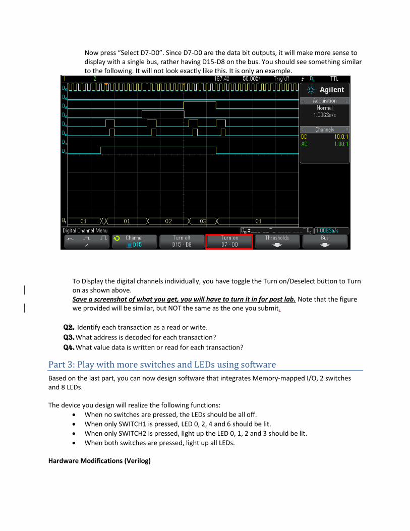
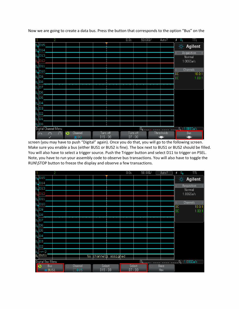
Now press “Select D7-D0”. Since D7-D0 are the data bit outputs, it will make more sense to display with a single bus, rather having D15-D8 on the bus. You should see something similar to the following. It will not look exactly like this. It is only an example.
To Display the digital channels individually, you have toggle the Turn on/Deselect button to Turn on as shown above. Save a screenshot of what you get, you will have to turn it in for post lab. Note that the figure we provided will be similar, but NOT the same as the one you submit.
Q2. Identify each transaction as a read or write.
Q3. What address is decoded for each transaction?
Q4. What value data is written or read for each transaction?
Part 3: Play with more switches and LEDs using software
Based on the last part, you can now design software that integrates Memory-mapped I/O, 2 switches and 8 LEDs. The device you design will realize the following functions:
When no switches are pressed, the LEDs should be all off.
When only SWITCH1 is pressed, LED 0, 2, 4 and 6 should be lit.
When only SWITCH2 is pressed, light up the LED 0, 1, 2 and 3 should be lit.
When both switches are pressed, light up all LEDs. Hardware Modifications (Verilog)
Add the extra switch and LEDs connections to your existing MMIO registers. The hardware should only provide the readings of the switches by the processor and the writing of the LEDs by the processor (the software/assembly will do the rest). Software Modifications (Assembly) Modify the software to implement the functionality specified above using your updated MMIO. For example, read the switch in assembly and write the LEDs accordingly.
G2. Demonstrate your program to your lab instructor.
Part 4: PWM Design while using a servo motor
In this part, your task is to design hardware and software which uses the two buttons on the board to adjust the position of a servo. The hardware will perform the PWM function. A Verilog example is provided below. A register interfaced to the APB3 buss will allow you to change the duty cycle. You will also read switches as you did before onto the APB3 buss. The software will use the switch information to determine what control signals to send to the servo to move it one way or another.
Overview and background
1. PWM and duty cycle The basic idea of PWM is to manipulate the high and low of a pulse, and the term duty cycle is what we use to describe the proportion of time that a signal is being pulled “high” in one cycle. For example, the period of a 100Hz signal is 0.01s, and if the signal has 0.005s of “high” and 0.005s of “low” in each cycle, we say it has “50% duty cycle”. If it were high for .009s and low for .001s it would have a 90% duty cycle (it is high 90% of the time). 2. Servo Motors The basic way to control a servo motor is to adjust the duty cycle. Each brand of motor has its unique pulse cycle and pulse width which found in their product specification. For example, the most common motor we use in lab is Hitec HS-422, the link below is the spec: http://www.servodatabase.com/servo/hitec/hs-422
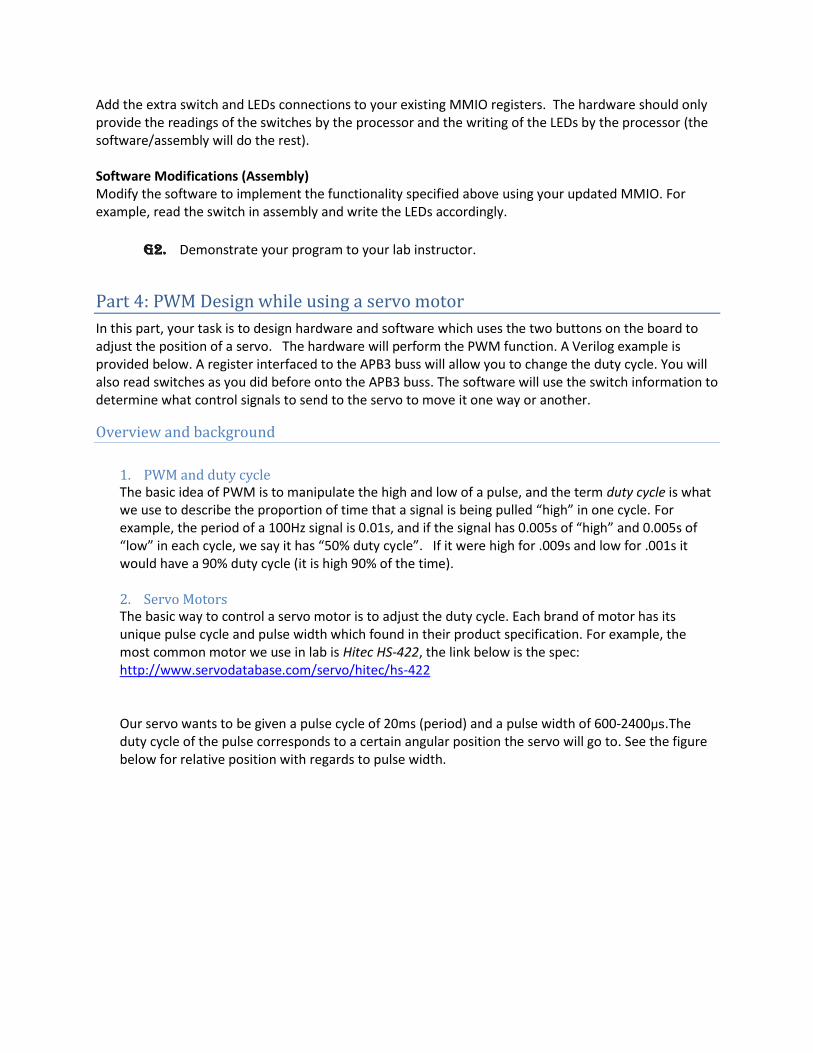
Our servo wants to be given a pulse cycle of 20ms (period) and a pulse width of 600-2400µs.The duty cycle of the pulse corresponds to a certain angular position the servo will go to. See the figure below for relative position with regards to pulse width.
Note that the minimum duty cycle for servo motor will NOT generally be 0%, nor the max 100%! You will have to calculate the max and min duty cycle with the information from the specification for the part you are working with.
Q5. What is the frequency of the pulse that HS-422 requires?
Q6. What is the duty cycle with pulse width 600µs? How about 2400µs?
3. PWM Verilog The following Verilog is provided as a starting point or reference design for a PWM generator. You will have to change the values to accommodate the servos specific requirements. This example provides a duty cycle of 20% with a pulse period of 50 x clk period. You will also need to provide a memory mapped register to control the duty cycle from software.
module pwm(
input clk,
output reg pwm
);
`define pulseWidth 10
`define period 50
reg [31:0] count;
always @(posedge clk)
begin
if (count == `period)
count <= 0;
else
count <= count + 1;
if (count < `pulseWidth)
pwm <= 1;
else
pwm <= 0;
Pulse Width
0.6ms
2.4ms
end
endmodule
Q7. What value should period be to satisfy the servo pulse frequency (or period) requirement? Assume a clock frequency of 100 Mhz.
Q8. What value should pulseWidth be to provide a duty cycle of 50%?
Q9. What has to be a register in the PWM code to provide software control of the duty cycle?
4. Debouncer To control the servo, you will need to detect push button transitions or edges. Because of the switch bounce, more than one high to low transition can occur for a single switch press or release (the redundant transitions are called “glitches”). To eliminate the effect of the “glitches”, we will first synchronize the switch to the system clock and then sample the switch after an estimated bounce time. One way to do this is discussed here: http://www.fpga4fun.com/Debouncer.html A simpler version of that code is provided below. Use PCLK for the clk., bouncy switch source for PB_in and debounced switch for PB_out.
//
// *** Button debouncer. ***
// Changes in the input are ignored until they have been consistent for 2^16 clocks.
//
Module Button_Debouncer(
input clk,
input PB_in, // button input
output reg PB_out // debounced output
);
reg [15:0] PB_cnt; // 16-bit counter
reg [1:0] sync; // used as two flip-flops to synchronize
// button to the clk domain.
// First use two flipflops to synchronize the PB signal the "clk" clock domain
always @(posedge clk)
sync[1:0] <= {sync[0],~PB_in};
wire PB_idle = (PB_out==sync[1]); // See if we have a new input state for PB
wire PB_cnt_max = &PB_cnt; // true when all bits of PB_cnt are 1's
// using & in this way is a
// "reduction operation"
// When the push-button is pushed or released, we increment the counter.
// The counter has to be maxed out before we decide that the push-button
// state has changed
always @(posedge clk) begin
if(PB_idle)
PB_cnt<= 16'd0; // input and output are the same so clear counter
else begin
PB_cnt<= PB_cnt + 16'd1; // input different than output, count
if(PB_cnt_max)
PB_out<= ~PB_out; // if the counter is maxed out,
// change PB output
end
end
endmodule
Q10. “sync” is being used to “synchronize the push buttons to the clock domain”. a. What does that mean? b. How is it doing that?
Q11. What is a “reduction operation” in Verilog? How is it being used here?
Building the device
Design a device that:
When SWITCH1 is pressed once, the motor will rotate 10 degrees CW.
When SWITCH2 is pressed once, the motor will rotate 10 degrees CCW.
The motor will stay still if it has reached the minimum or maximum rotation degrees (0 and 180 degrees).
You may design the device by separating the MMIO modules by their functionalities. One for reading the switches, one for PWM output…etc.
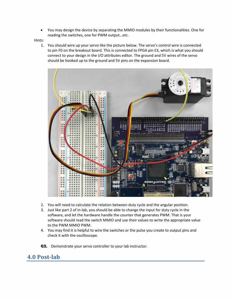
Hints: 1. You should wire up your servo like the picture below. The servo’s control wire is connected
to pin F0 on the breakout board. This is connected to FPGA pin E3, which is what you should connect to your design in the I/O attributes editor. The ground and 5V wires of the servo should be hooked up to the ground and 5V pins on the expansion board.
2. You will need to calculate the relation between duty cycle and the angular position. 3. Just like part 2 of in-lab, you should be able to change the input for duty cycle in the
software, and let the hardware handle the counter that generates PWM. That is your software should read the switch MMIO and use their values to write the appropriate value to the PWM MMIO PWM.
4. You may find it is helpful to wire the switches or the pulse you create to output pins and check it with the oscilloscope.
G3. Demonstrate your servo controller to your lab instructor.
4.0 Post-lab
Q12. In part 4 of the in-lab, theoretically you could create PWM purely in software using the software clock and send 1’s and 0’s to the motor in a while loop. This is what is called “bit-banging”(http://en.wikipedia.org/wiki/Bit_banging). What are the pros and cons of this method?
Q13. Though we did not do bit-banging in this lab, we still have to continuously check the switches with loops. Realistically, given that a human will be using the switches, how often do we need to poll the switches to see if they have been pressed or released? Explain how you arrived at your answer.
5.0 Conclusion
As you may have noticed, even though the hardware is controlling the servo, we still have a loop that is checking to see if a button was pressed.. What’s worse is that the validity of your program depends on how fast a person can press the switch! That doesn’t seem too promising, does it? As your program grows larger and has to handle more tasks, it become obvious that continuous polling of all devices is not the best idea. A processor should be able to handle more than one task. So, this leads us to our next topic: Interrupts. An interrupt is like a conditional case, such that the code will be executed only when a certain event occur, at any time while the machine is running. In this case, if we have the switch detection as an interrupt event, our processor can be working on something else if switches are not being pressed. Also we do not have to worry about missing any switch press, because interrupt will queue all the events that occur. Finally, it is important to think about how you managed to have the software and hardware work together in this lab. In general, hardware is well suited to continuous tasks (such as driving the PWM signal) while software is better suiting to more complex tasks, which we really didn’t have in this lab. So imagine we were trying to create a device that implemented a complex control algorithm (such as keeping an inverted pendulum2 upright).That type of algorithm could be very difficult to implement in hardware. The concept of partitioning the work between the hardware and software will prove to be crucial when it comes to your final project design. And even if you have a design that partitioned the work in a good and reasonable way, you still need to get the two parts to work together. During this lab you have seen how to have software control the hardware.
2 See http://en.wikipedia.org/wiki/Inverted_pendulum.