eecs 270 midterm 1 exam closed book portion · eecs 270 midterm 1 exam closed book portion fall...
TRANSCRIPT
Page 1 of 12
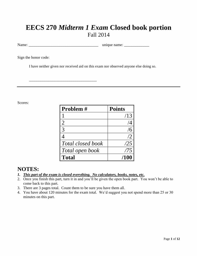
EECS 270 Midterm 1 Exam Closed book portion Fall 2014
Name: ____________________________________ unique name: _____________
Sign the honor code:
I have neither given nor received aid on this exam nor observed anyone else doing so.
___________________________________
Scores:
Problem # Points
1 /13
2 /4
3 /6
4 /2
Total closed book /25
Total open book /75
Total /100
NOTES: 1. This part of the exam is closed everything. No calculators, books, notes, etc.
2. Once you finish this part, turn it in and you’ll be given the open book part. You won’t be able to
come back to this part.
3. There are 3 pages total. Count them to be sure you have them all.
4. You have about 120 minutes for the exam total. We’d suggest you not spend more than 25 or 30
minutes on this part.
Page 2 of 12
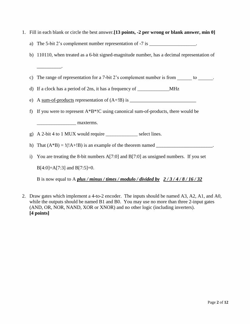
1. Fill in each blank or circle the best answer.[13 points, -2 per wrong or blank answer, min 0]
a) The 5-bit 2’s complement number representation of -7 is ___________________.
b) 110110, when treated as a 6-bit signed-magnitude number, has a decimal representation of
__________.
c) The range of representation for a 7-bit 2’s complement number is from ______ to ______.
d) If a clock has a period of 2ns, it has a frequency of _____________MHz
e) A sum-of-products representation of (A+!B) is ___________________________
f) If you were to represent A*B*!C using canonical sum-of-products, there would be
________________ maxterms.
g) A 2-bit 4 to 1 MUX would require _____________ select lines.
h) That (A*B) = !(!A+!B) is an example of the theorem named _______________________.
i) You are treating the 8-bit numbers A[7:0] and B[7:0] as unsigned numbers. If you set
B[4:0]=A[7:3] and B[7:5]=0.
B is now equal to A plus / minus / times / modulo / divided by 2 / 3 / 4 / 8 / 16 / 32
2. Draw gates which implement a 4-to-2 encoder. The inputs should be named A3, A2, A1, and A0,
while the outputs should be named B1 and B0. You may use no more than three 2-input gates
(AND, OR, NOR, NAND, XOR or XNOR) and no other logic (including inverters).
[4 points]
Page 3 of 12
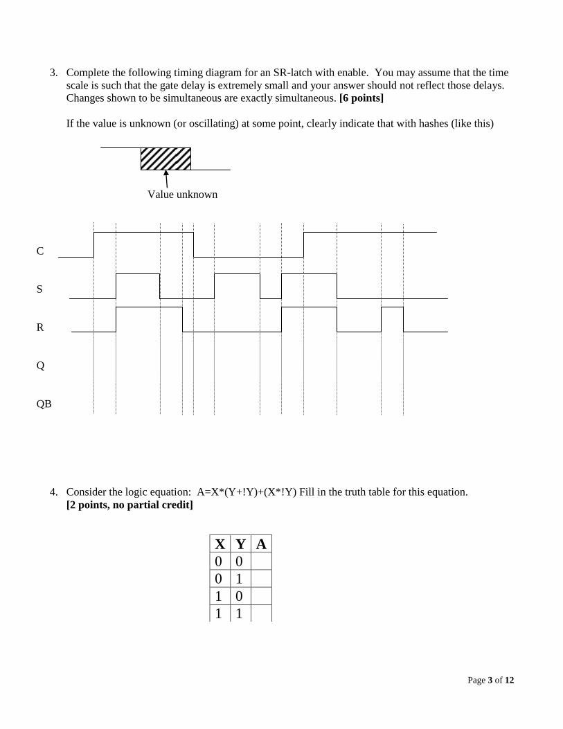
3. Complete the following timing diagram for an SR-latch with enable. You may assume that the time
scale is such that the gate delay is extremely small and your answer should not reflect those delays.
Changes shown to be simultaneous are exactly simultaneous. [6 points]
If the value is unknown (or oscillating) at some point, clearly indicate that with hashes (like this)
4. Consider the logic equation: A=X*(Y+!Y)+(X*!Y) Fill in the truth table for this equation.
[2 points, no partial credit]
X Y A
0 0
0 1
1 0
1 1
C
S
R
Q
QB
Value unknown
Page 4 of 12
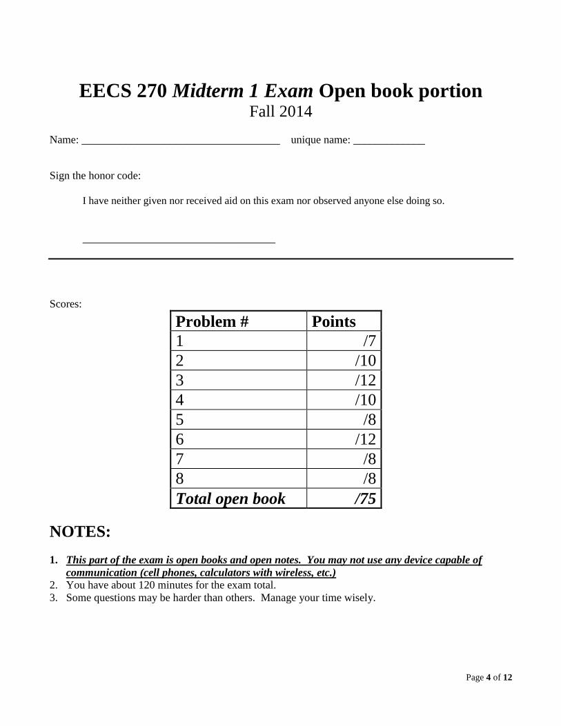
EECS 270 Midterm 1 Exam Open book portion Fall 2014
Name: ____________________________________ unique name: _____________
Sign the honor code:
I have neither given nor received aid on this exam nor observed anyone else doing so.
___________________________________
Scores:
Problem # Points
1 /7
2 /10
3 /12
4 /10
5 /8
6 /12
7 /8
8 /8
Total open book /75
NOTES:
1. This part of the exam is open books and open notes. You may not use any device capable of
communication (cell phones, calculators with wireless, etc.)
2. You have about 120 minutes for the exam total.
3. Some questions may be harder than others. Manage your time wisely.

Page 5 of 12
1) Design a state transition diagram for a state machine that takes two inputs, A and B and has one
output, X. X is to be a 1 if, and only if, A has been the same as B for the last two clock periods.
[7 points]
So if A=000111001
B=100100001
X=001100011

Page 6 of 12
2) Design a state transition diagram for a state machine that takes one input, A and has one output, X.
X should be a 1 if, and only if, the last four values of A have been either 1011, 1001, or 0100.
[10 points]
Page 7 of 12
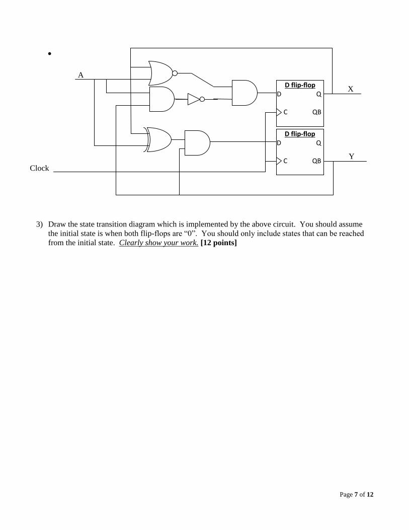
3) Draw the state transition diagram which is implemented by the above circuit. You should assume
the initial state is when both flip-flops are “0”. You should only include states that can be reached
from the initial state. Clearly show your work. [12 points]
Clock
X
A
Y
D flip-flop D Q C QB
D flip-flop D Q C QB
Page 8 of 12
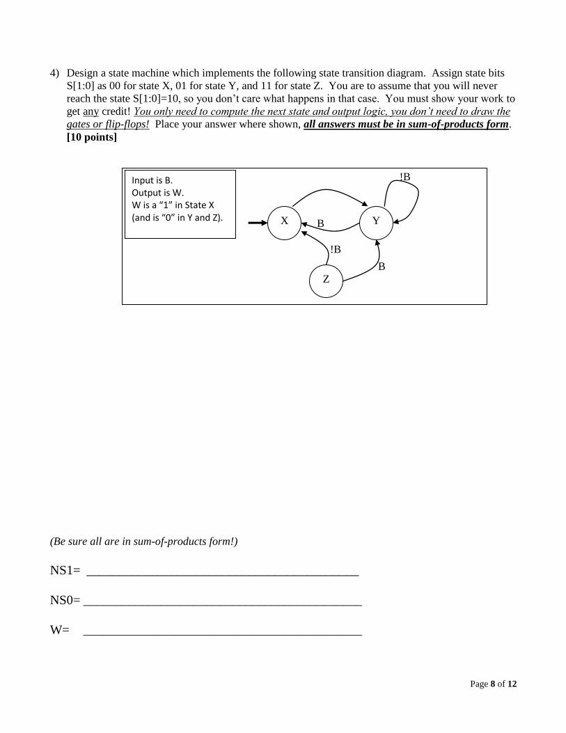
4) Design a state machine which implements the following state transition diagram. Assign state bits
S[1:0] as 00 for state X, 01 for state Y, and 11 for state Z. You are to assume that you will never
reach the state S[1:0]=10, so you don’t care what happens in that case. You must show your work to
get any credit! You only need to compute the next state and output logic, you don’t need to draw the
gates or flip-flops! Place your answer where shown, all answers must be in sum-of-products form.
[10 points]
(Be sure all are in sum-of-products form!)
NS1= __________________________________________
NS0= ___________________________________________
W= ___________________________________________
X Y
Z
!B
B
!B
B
Input is B. Output is W. W is a “1” in State X (and is “0” in Y and Z).

Page 9 of 12
5) Implement a 2-input XOR using only 2-input NAND gates. For full credit, use 5 or fewer NAND
gates. Use assume the inputs are labeled A and B while the output is labeled X.
[8 points, half credit for using more than 5 gates]
Page 10 of 12
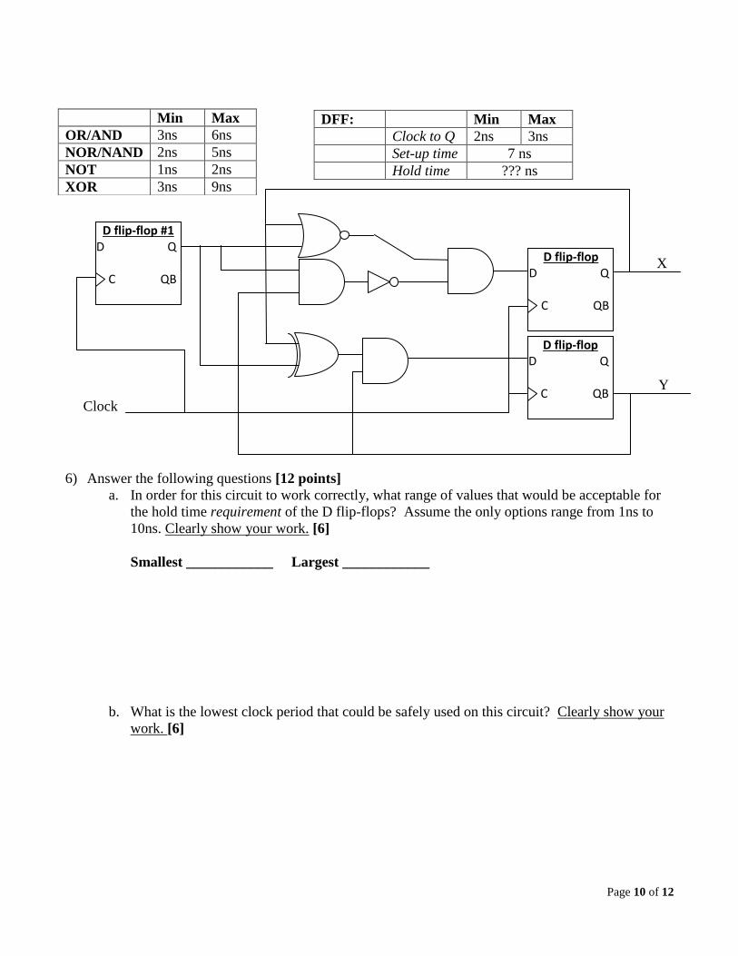
6) Answer the following questions [12 points]
a. In order for this circuit to work correctly, what range of values that would be acceptable for
the hold time requirement of the D flip-flops? Assume the only options range from 1ns to
10ns. Clearly show your work. [6]
Smallest ____________ Largest ____________
b. What is the lowest clock period that could be safely used on this circuit? Clearly show your
work. [6]
DFF: Min Max
Clock to Q 2ns 3ns
Set-up time 7 ns
Hold time ??? ns
Min Max
OR/AND 3ns 6ns
NOR/NAND 2ns 5ns
NOT 1ns 2ns
XOR 3ns 9ns
Clock
X
A
Y
D flip-flop D Q C QB
D flip-flop D Q C QB
D flip-flop #1 D Q C QB
Page 11 of 12
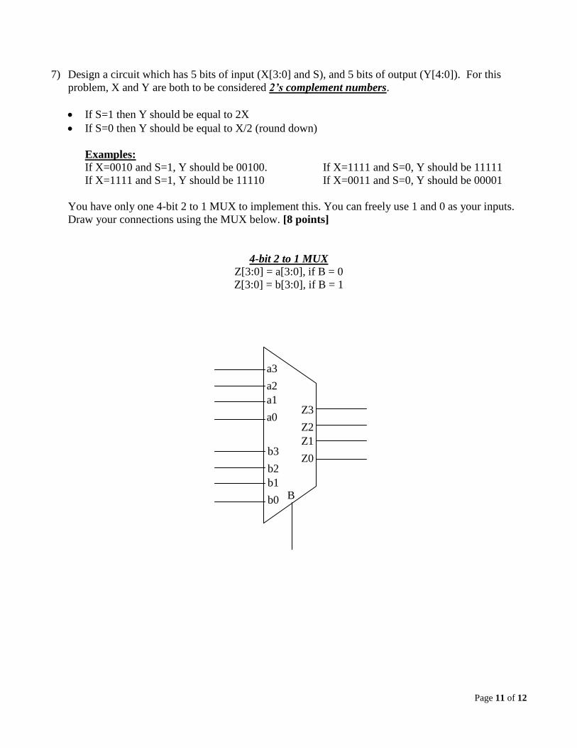
7) Design a circuit which has 5 bits of input (X[3:0] and S), and 5 bits of output (Y[4:0]). For this
problem, X and Y are both to be considered 2’s complement numbers.
If S=1 then Y should be equal to 2X
If S=0 then Y should be equal to X/2 (round down)
Examples:
If X=0010 and S=1, Y should be 00100. If X=1111 and S=0, Y should be 11111
If X=1111 and S=1, Y should be 11110 If X=0011 and S=0, Y should be 00001
You have only one 4-bit 2 to 1 MUX to implement this. You can freely use 1 and 0 as your inputs.
Draw your connections using the MUX below. [8 points]
4-bit 2 to 1 MUX
Z[3:0] = a[3:0], if B = 0
Z[3:0] = b[3:0], if B = 1
B
a3
a2
a1
a0
b3
b2
b1
b0
Z3
Z2
Z1
Z0
Page 12 of 12
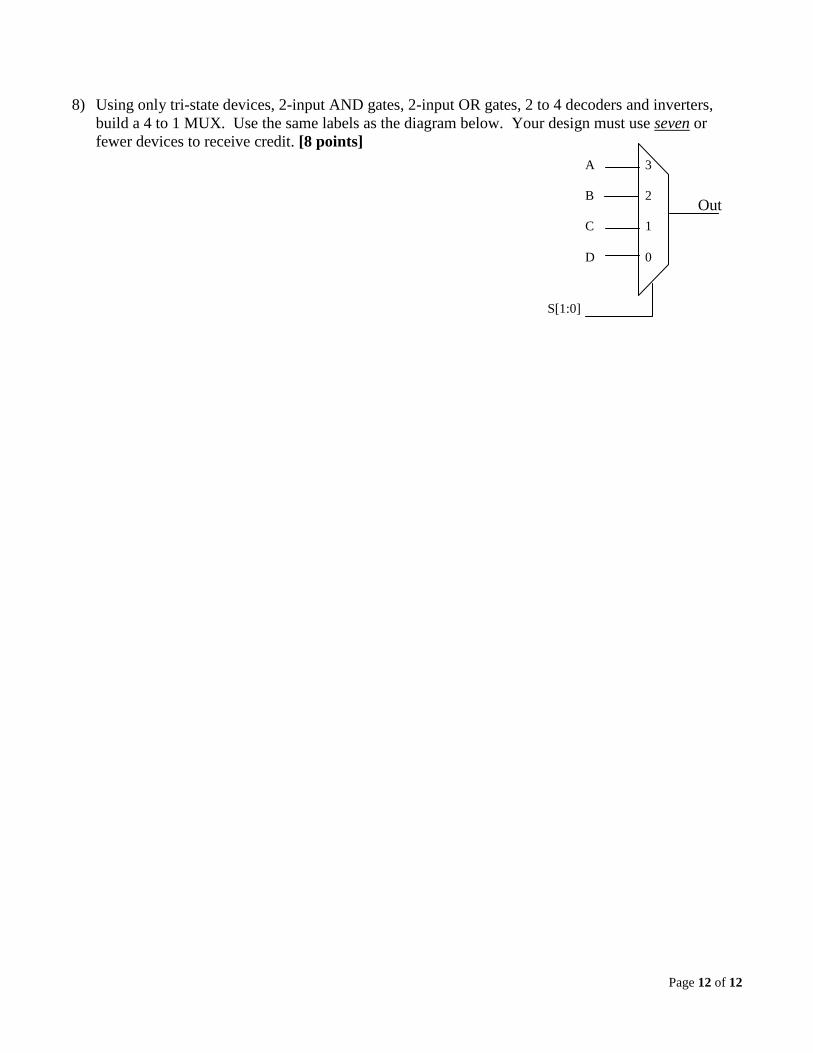
8) Using only tri-state devices, 2-input AND gates, 2-input OR gates, 2 to 4 decoders and inverters,
build a 4 to 1 MUX. Use the same labels as the diagram below. Your design must use seven or
fewer devices to receive credit. [8 points]
A
B
C
D
3
2
1
0
Out
S[1:0]