edward t. yu · curriculum vitae edward t. yu august 2019 2 vice-chair, electrical and computer...
TRANSCRIPT

Curriculum Vitae August 2019
Edward T. Yu Professor of Electrical & Computer Engineering
Judson S. Swearingen Regents Chair in Engineering Director, Center for Dynamics and Control of Materials: an NSF MRSEC
The University of Texas at Austin
The University of Texas at Austin Tel (O): +1.512.232.5167Building 160, MER 1.206M Fax (O): +1.512.471.896910100 Burnet Road e-mail: [email protected], TX 78758 WWW: http://etylab.ece.utexas.edu
https://mrsec.utexas.edu Citizenship: United States
Research Interests Edward Yu directs a research laboratory concerned generally with the characterization, understanding, and application of physical phenomena in solid-state materials and device structures at nanometer to atomic length scales. Current research interests in his group include the following:
• solid-state nanostructure physics, materials, and devices • photovoltaics and other technologies for energy harvesting, generation, and storage • nanoscale imaging and characterization techniques, particularly based on proximal probes • dynamic control and reconfigurability of materials functionality
Education California Institute of Technology, Pasadena, CA Ph.D. (Applied Physics) ADVISOR: Professor Thomas C. McGill
June 1991
Harvard University, Cambridge, MA A.M. (Physics) June 1986Harvard University, Cambridge, MA A.B. (Physics, summa cum laude) June 1986
Professional Experience PROFESSOR and JUDSON S. SWEARINGEN REGENTS CHAIR IN ENGINEERING, The University of Texas at Austin
2009 –
DIRECTOR, Center for Dynamics and Control of Materials: an NSF MRSEC 2017 –
ADJUNCT PROFESSOR, Electrical and Computer Engineering University of California, San Diego
2009 –16
PROFESSOR, Electrical and Computer Engineering University of California, San Diego
1998 − 2009
ASSOCIATE DIRECTOR, Center for Energy Research University of California, San Diego
2008 –09
ASSOCIATE PROFESSOR, Electrical and Computer Engineering University of California, San Diego
1996 –98
ASSISTANT PROFESSOR, Electrical and Computer Engineering University of California, San Diego
1992 –96
Curriculum Vitae Edward T. Yu August 2019
2
VICE-CHAIR, Electrical and Computer Engineering University of California, San Diego
2000
VISITING PROFESSOR, Electrical Engineering Stanford University
1999
VISITING ASSOCIATE, Applied Physics California Institute of Technology
1999
POSTDOCTORAL FELLOW, IBM T. J. Watson Research Center ADVISOR: Dr. Jean-Marc Halbout
1991 – 92
POSTDOCTORAL FELLOW, California Institute of Technology ADVISOR: Professor Thomas C. McGill
1991
Academic and Professional Honors Fellow, IEEE 2012
Fellow, AVS 2009
Outstanding Speaker Award, Tri-Services Workshop on Process Induced Defects in Wide Bandgap Semiconductors
2003
Outstanding Speaker Award, ONR Workshop on Extended Defects in Wide Gap Semiconductors II
2003
Member, Defense Science Study Group 2000 − 01Office of Naval Research Young Investigator Award 1995 − 98Alfred P. Sloan Research Fellowship 1995 − 97National Science Foundation CAREER Award 1995 − 99ECE Graduate Teaching Award 1997AT&T Bell Laboratories Ph.D. Scholarship 1989 – 91National Science Foundation Graduate Fellowship 1986 –89Phi Beta Kappa, Harvard University 1985
Professional Activities Member/Chair:
Chair, DARPA Defense Sciences Research Council (DSRC), 2012 – 14 Associate Chair/Chair-elect, DARPA Defense Sciences Research Council (DSRC), 2010 – 12 Member, DARPA Defense Sciences Research Council (DSRC), 2007 – 16 Fellow, DARPA Defense Sciences Research Council (DSRC), 2005-2007 Member, Defense Science Study Group (DSSG), 2000-2001 Program Chair, AVS Nanometer-Scale Science and Technology Division, 2003-04; Division Chair, 2002-03; Vice-Chair/Chair-elect, 2001-02; Member-at-Large, Division Board, 1998-2000 General Chair, TMS Electronic Materials Committee, 2005–07; Vice-Chair/Program Chair, 2003-05; Secretary, 2001–03; Past Chair, 2007-09; Member, 1998-2009; Member-at-Large, 2009 – present American Physical Society Fellow, American Vacuum Society (AVS)

Curriculum Vitae Edward T. Yu August 2019
3
Böhmische Physical Society Fellow, IEEE Materials Research Society
Conference Chair: Program Chair, Conference on Physics and Chemistry of Semiconductor Interfaces (PCSI), 2002 Program Chair, Electronic Materials Conference, 2004 and 2005 General Chair, Electronic Materials Conference, 2006 and 2007
Program Committee Member (partial list): Electronic Materials Conference, 1995-present Conference on Physics and Chemistry of Semiconductor Interfaces (PCSI), 2001- CIMTEC 2010, 5th Forum on New Materials (International Advisory Board), 2010 SPIE Optics+Photonics: Solar Energy + Technology, Next Generation (Nano) Photonic and Cell Technologies for Solar Energy Conversion, 2010 International Conference on InP and Related Materials, 2009 International Conference on Nitride Semiconductors (ICNS-7), 2007 Sixth International Conference on Nanometer-Scale Science and Technology, 2000 AVS National Symposium, Nanometer-Scale Science and Technology Division, 1999-2000, 2003-04 SPIE Symposium on Instrumentation and Techniques for Nanoscale Materials and Applications, 1999-2000 IEEE MTT-S International Microwave Symposium, 1994
Symposium Organizer: 1998 Spring Meeting, Materials Research Society 2001 Spring Meeting, Materials Research Society 2002 Fall Meeting, Materials Research Society
Guest Editor: MRS Bulletin Special Issue on Nanoscale Characterization of Materials (August 1997) MRS Bulletin Special Issue on Photon Management in Photovoltaics (June 2011)
Editorial Board Member: International Journal of Modern Physics B/Modern Physics Letters B Materials Science and Engineering Reports IEEE Transactions on Nanotechnology
Reviewer: Applied Physics Letters, IEEE Transactions on Microwave Theory and Techniques, IEEE Electron Device Letters, IEEE Transactions on Electron Devices, IEEE Transactions on Nanotechnology, Journal of Applied Physics, Journal of Vacuum Science and Technology, Micron, Nano Letters, Nature Communications, Nature Nanotechnology, Physical Review B, Review of Scientific Instruments, etc.

Curriculum Vitae Edward T. Yu August 2019
4
National Science Foundation, Department of Energy, UC MICRO program, UC SMART program, etc.
Teaching Experience University of California, San Diego
1992-1993: ECE 5B: Our Natural and Artificial Environment – Computers (W, introductory/nonmajor level) ECE 121C: Electromagnetism III (S, senior level)
1993-1994: ECE 239: Nanometer-Scale Probes and Devices (F, advanced graduate level) ECE 5B: Our Natural and Artificial Environment – Computers (W, introductory/nonmajor level) ECE 121C: Electromagnetism III (S, senior level) ECE 138: Introduction to Semiconductor Devices (S, senior level)
1994-95: ECE 138: Introduction to Semiconductor Devices (F, senior level) ECE 5B: Our Natural and Artificial Environment – Computers (W, introductory/nonmajor level) ECE 121C: Electromagnetism III (S, senior level)
1995-96: ECE 103: Fundamentals of Devices and Materials (F, junior level) ECE 5B: Our Natural and Artificial Environment – Computers (W, introductory/nonmajor level)
1996-97: ECE 103: Fundamentals of Devices and Materials (F, junior level) ECE 136: Fundamentals of Semiconductor Device Fabrication (W, senior level) ECE 230C: Solid State Electronics III (S, graduate level)
1997-98: ECE 103: Fundamentals of Devices and Materials (F, junior level) ECE 134: Electronic Materials Science of Integrated Circuits (W, senior level) ECE 230C: Solid State Electronics III (S, graduate level)
1998-99: ECE 103: Fundamentals of Devices and Materials (F, junior level) Sabbatical leave (W) ECE 230C: Solid State Electronics III (S, graduate level)
1999-2000: ECE 103: Fundamentals of Devices and Materials (F, junior level) ECE 136: Fundamentals of Semiconductor Device Fabrication (W, senior level) ECE 230C: Solid State Electronics III (S, graduate level)

Curriculum Vitae Edward T. Yu August 2019
5
2000-2001: ECE 103: Fundamentals of Devices and Materials (F, junior level) ECE 134: Electronic Materials Science of Integrated Circuits (W, senior level) ECE 230C: Solid State Electronics III (S, graduate level)
2001-2002: ECE 103: Fundamentals of Devices and Materials (F, junior level) Course relief due to heavy University service (W) ECE 230C: Solid State Electronics III (S, graduate level)
2002-2003: ECE 103: Fundamentals of Devices and Materials (F, junior level) Course relief due to heavy University service (W) ECE 230C: Solid State Electronics III (S, graduate level)
2003-2004: ECE 135A: Semiconductor Physics (F, senior level) ECE 135B: Electronic Devices (W, senior level) ECE 230C: Solid State Electronics III (S, graduate level)
2004-2005: ECE 135A: Semiconductor Physics (F, senior level) ECE 236A: Semiconductor Heterostructure Materials (F, graduate level) ECE 135B: Electronic Devices (W, senior level) ECE 230C: Solid State Electronics III (S, graduate level)
2005-2006: ECE 236A: Semiconductor Heterostructure Materials (F, graduate level) Sabbatical leave (W) ECE 230C: Solid State Electronics III (S, graduate level) ECE 294: Solid-State Electronics Graduate Seminar (S, graduate level)
2006-2007: ECE 135A: Semiconductor Physics (F, senior level) ECE 236A: Semiconductor Heterostructure Materials (W, graduate level) ECE 230C: Solid State Electronics III (S, graduate level)
2007-2008: ECE 212A: Principles of Nanoscience (F, graduate level) ECE 236A: Semiconductor Heterostructure Materials (W, graduate level) ECE 230C: Solid State Electronics III (S, graduate level)
2008-2009: ECE 212A: Principles of Nanoscience (F, graduate level) ECE 135B: Electronic Devices (W, senior level) ECE 230C: Solid State Electronics III (S, graduate level)

Curriculum Vitae Edward T. Yu August 2019
6
The University of Texas at Austin
2009-2010: EE 396K-23: Semiconductor Heterostructures (F, graduate level) EE 396V: Advanced Solid-State Materials and Nanostructures (S, graduate level)
2010-2011: EE 302: Introduction to Electrical Engineering (F, freshman level) EE 396K-23: Semiconductor Heterostructures (S, graduate level)
2011-2012: EE 302: Introduction to Electrical Engineering (F, freshman level) EE 396K-23: Semiconductor Heterostructures (S, graduate level)
2012-2013: EE 302: Introduction to Electrical Engineering (F, freshman level) EE 396K-23: Semiconductor Heterostructures (S, graduate level) Faculty Advisor, ECE Senior Design Project Team (S)
2013-2014: EE 302: Introduction to Electrical Engineering (F, freshman level) EE 396K-23: Semiconductor Heterostructures (S, graduate level) Faculty Advisor, ECE Senior Design Project Team (F)
2014-2015: EE 302: Introduction to Electrical Engineering (F, freshman level) EE 396K-23: Semiconductor Heterostructures (S, graduate level) Faculty Advisor, ECE Senior Design Project Team (F, S)
2015-2016: EE 302: Introduction to Electrical Engineering (F, freshman level) EE 396K-23: Semiconductor Heterostructures (S, graduate level) Faculty Advisor, ECE Senior Design Project Team (F, S)
2016-2017: Course relief for large extramural proposal development (F) EE 302: Introduction to Electrical Engineering (S, freshman level) Faculty Advisor, ECE Senior Design Project Team (F, S)
2017-2018: EE 302: Introduction to Electrical Engineering (F, freshman level) EE 396K-23: Semiconductor Heterostructures (S, graduate level)
2018-2019: EE 302: Introduction to Electrical Engineering (F, freshman level) Course relief for MRSEC directorship (S)

Curriculum Vitae Edward T. Yu August 2019
7
2019-2020: EE 302: Introduction to Electrical Engineering (F, freshman level) EE 396K-23: Semiconductor Heterostructures (S, graduate level)
Departmental and University Service University of California, San Diego
1992-1993: Examiner, ECE Graduate Comprehensive Exam (Quantum Theory, Spring 1993)
1993-1994: Examiner, ECE Graduate Comprehensive Exam (Quantum Theory, Fall 1993, Spring 1994) Undergraduate Academic Advisor, Engineering Physics Program
1994-1995: Member, ECE Undergraduate Affairs Committee Member, ECE Graduate Admissions Committee Initiator and Coordinator, ECE WWW site Coordinator, Materials Science Graduate Qualifying Exam, Spring 1995 Undergraduate Academic Advisor, Engineering Physics Program
1995-1996: Member, Executive Committee, UCSD Materials Science Program Member and Chair, ECE Web Site Committee Member, ECE Undergraduate Affairs Committee Member, ECE Computer Committee Member, ECE Graduate Admissions Committee Undergraduate Academic Advisor, Engineering Physics Program Faculty Advisor, UCSD IEEE Student Chapter
1996-1997: Member, Executive Committee, UCSD Materials Science Program Member and Chair, ECE Web Site Committee Member, ECE Undergraduate Affairs Committee Member, ECE Computer Committee Member, ECE Graduate Admissions Committee Undergraduate Academic Advisor, Engineering Physics Program Faculty Advisor, UCSD IEEE Student Chapter
1997-1998: Member, Executive Committee, UCSD Materials Science Program Member and Chair, ECE Web Site Committee Member, ECE Undergraduate Affairs Committee Member, ECE Computer Committee

Curriculum Vitae Edward T. Yu August 2019
8
Member, ECE Graduate Admissions Committee Undergraduate Academic Advisor, Engineering Physics Program Faculty Advisor, UCSD IEEE Student Chapter
1998-1999: Member, Executive Committee, UCSD Materials Science Program Member and Chair, ECE Web Site Committee Member, ECE Undergraduate Affairs Committee Member, ECE Computer Committee Member, ECE Graduate Admissions Committee Undergraduate Academic Advisor, Engineering Physics Program Faculty Advisor, UCSD IEEE Student Chapter
1999-2000: Vice Chair/Student Affairs, ECE Department (Winter & Spring 2000) Member, Executive Committee, UCSD Materials Science Program Search Committee Member, Kazuo Iwama Chair in Materials Science Search Committee Member, Director of the Center for Magnetic Recording Research Member, UCSD University Graduate Fellowship Committee Member and Chair, ECE Graduate Affairs Committee Member, ECE Graduate Admissions Committee Undergraduate Academic Advisor, Engineering Physics Program Faculty Advisor, UCSD IEEE Student Chapter
2000-2001: Member, Executive Committee, UCSD Materials Science Program Search Committee Member, Kazuo Iwama Chair in Materials Science Member, Committee on Ethos and Culture of the Jacobs School of Engineering, UCSD Member and Chair, ECE Graduate Affairs Committee Member, ECE Graduate Admissions Committee Undergraduate Academic Advisor, Engineering Physics Program Faculty Advisor, UCSD IEEE Student Chapter
2001-2002: Member, Executive Committee, UCSD Materials Science Program Member, UCSD Academic Senate Committee on Academic Personnel* Chair, Sunset Review Committee for UCSD Center for Magnetic Recording Research Search Committee (observing member), Kazuo Iwama Chair in Materials Science Search Committee (observing member), ECE Electronic Devices and Materials faculty search Member (FWS) and Chair (F), ECE Graduate Affairs Committee
* This is the committee that reviews and makes recommendations for personnel actions (appointment, promotion, acceleration, etc.) for all academic personnel at UCSD, including SOM and SIO. Approximately 600 cases/year were considered at that time.

Curriculum Vitae Edward T. Yu August 2019
9
Member, ECE Graduate Admissions Committee Member, ECE Faculty Council** Undergraduate Academic Advisor, Engineering Physics Program Faculty Advisor, UCSD IEEE Student Chapter
2002-03: Member, Executive Committee, UCSD Materials Science Program Vice-Chair, UCSD Academic Senate Committee on Academic Personnel* Member, University of California Committee on Academic Personnel (WS) Search Committee (observing member), ECE Electronic Devices and Materials faculty search Member, ECE Graduate Affairs Committee Member, ECE Graduate Admissions Committee Undergraduate Academic Advisor, Engineering Physics Program
2003-04: Member, Executive Committee, UCSD Materials Science and Engineering Program Member (F), UCSD Academic Senate Committee on Academic Personnel* Member, ECE Graduate Affairs Committee Member, ECE Graduate Admissions Committee Member, ECE Computer Committee Undergraduate Academic Advisor, Engineering Physics Program
2004-05: Member, Executive Committee, UCSD Materials Science and Engineering Program Vice-Chair, UCSD Academic Senate Committee on Admissions Member, ECE Graduate Affairs Committee Chair, ECE Graduate Admissions Committee Member, ECE Departmental Faculty Recruiting Committee Member, ECE Faculty Search Committee in Micro/Nanotechnology Member, ECE Faculty Workload Committee Member, CMRR Endowed Chair Search Committee Member (1), Chair (1), ECE Department ad hoc faculty review committees Undergraduate Academic Advisor, Engineering Physics Program and ECE Devices/Materials option
2005-06: Member, University of California IUCRP Executive Committee on Electronic Manufacturing/New Materials Member, Executive Committee, UCSD Materials Science and Engineering Program Chair (F), Member (W,S), ECE Graduate Admissions Committee Member, ECE Departmental Faculty Recruiting Committee Member, ECE Faculty Search Committee in Nano Devices/Materials
** This is the ECE faculty advisory committee to the Department Chair.

Curriculum Vitae Edward T. Yu August 2019
10
Member, ECE Faculty Workload Committee Member, CMRR Endowed Chair Search Committee Member (2), ECE Department ad hoc faculty review committees Undergraduate Academic Advisor, Engineering Physics Program and ECE Devices/Materials option
2006-07: Member, University of California IUCRP Executive Committee on Electronic Manufacturing/New Materials Member, Executive Committee, UCSD Materials Science and Engineering Program Member (F), UCSD Academic Senate Committee on Committees Member, UCSD Ethics Program Work Group Chair, ECE Graduate Admissions Committee Chair, ECE Faculty Search Committee in Nanotechnology Member, ECE Committee on Charting the Course IV (long-range planning) Member (3), ECE Department ad hoc faculty review committees Undergraduate Academic Advisor, Engineering Physics Program and ECE Devices/Materials option Graduate Academic Advisor, Applied Physics/Electronic Devices and Materials area
2007-08: Member, University of California IUCRP Executive Committee on Electronic Manufacturing/New Materials Member, Executive Committee, UCSD Materials Science and Engineering Program Member and Vice Chair, UCSD Academic Senate Committee on Admissions Chair, ECE Space Committee Member, ECE Faculty Search Committee in Nanotechnology Chair (1), Member (1), ECE Department ad hoc faculty review committees Undergraduate Academic Advisor, Engineering Physics Program and ECE Devices/Materials option Graduate Academic Advisor, Applied Physics/Electronic Devices and Materials area
2008-09: Associate Director, UCSD Center for Energy Research Chair, UCSD Academic Senate Committee on Admissions Member, UCSD Academic Senate Council Member, UCSD Academic Senate-Administration Council Member, UCSD Enrollment Planning Committee Member, University of California IUCRP Executive Committee on Electronic Manufacturing/New Materials Member, Executive Committee, UCSD Materials Science and Engineering Program Member, ECE Faculty Search Committee Member, Mechanical & Aerospace Engineering Faculty Search Committee in Energy Chair (1), ECE Department ad hoc faculty review committees Undergraduate Academic Advisor, Engineering Physics Program and ECE Devices/Materials option Graduate Academic Advisor, Nanoscale Devices & Systems area

Curriculum Vitae Edward T. Yu August 2019
11
The University of Texas at Austin
2010-11: Member, Cockrell School Promotion and Tenure Committee Member, Cockrell School Hocott Award Committee Member, EERC Space Policy Committee Member, ECE Faculty Search Committee Member, ECE Faculty Expectations Committee
2011-12: Chair, Cockrell School Promotion and Tenure Committee Member, Cockrell School Awards Committee Member, EERC Space Policy Committee Member, ECE Faculty Expectations Committee Member, ECE Teaching Awards Committee Member, ECE Faculty Search Committee
2012-13: Chair, ECE Faculty Search Committee Member, EERC Space Policy Committee Member, ECE Faculty Expectations Committee
2013-14: Member, ECE Faculty Search Committee, Dula Cockrell Centennial Chair in Engineering Member, EERC Space Policy Committee
2014-15: Member, ECE Faculty Search Committee, Dula Cockrell Centennial Chair in Engineering Member, EERC Space Policy Committee Member, Texas Materials Institute Facilities Committee Member, University of Texas Faculty Council Member, University of Texas Faculty Grievance Committee Member, University of Texas Faculty Building Advisory Committee
2015-16: Chair, ECE Faculty Search Committee Member, ECE Search Committee, Dula Cockrell Centennial Chair in Engineering Member, EERC Space Policy Committee Member, Texas Materials Institute Facilities Committee Member, University of Texas Faculty Council Member, University of Texas Faculty Grievance Committee Member, University of Texas Faculty Parking and Transportation Services Committee
2016-17: Chair, ECE Faculty Search Committee

Curriculum Vitae Edward T. Yu August 2019
12
Member, EERC Space Policy Committee Member, Texas Materials Institute Facilities Committee Member, University of Texas Faculty Grievance Committee Member, Ad Hoc Committee for Academic and Research Opportunities in Materials Science & Engineering Member, Materials Science & Engineering Minor Degree Committee Member, Ad Hoc Post-Tenure Review Committee for a Chair Professor in Cockrell School of Engineering
2017-18: Director, Center for Dynamics and Control of Materials: an NSF MRSEC Member, ECE Senior Faculty Search Committee Member, EERC Space Policy Committee Member, Texas Materials Institute Facilities and Executive Committee Member, Ad Hoc Committee for Academic and Research Opportunities in Materials Science & Engineering Member, UGS core curriculum assessment committee
2018-19: Director, Center for Dynamics and Control of Materials: an NSF MRSEC Member, ECE Department Chair Search Committee Member, EERC Space Policy Committee Member, Texas Materials Institute Facilities and Executive Committee Member, Ad Hoc Committee for Academic and Research Opportunities in Materials Science & Engineering
2018-19: Director, Center for Dynamics and Control of Materials: an NSF MRSEC Member, EERC Space Policy Committee Member, Texas Materials Institute Facilities and Executive Committee Member, Ad Hoc Committee for Academic and Research Opportunities in Materials Science & Engineering
Personnel Supervised:
Current Graduate Students:
Name Program/Department Prior Degree/Institution
Gabriel Cossio Ph.D. Candidate (Electrical Engineering), 2014 -
B.S., UT Austin (Physics), 2014
Alex De Palma Ph.D. Candidate (Materials Science & Engineering), 2016 -
B.S., SUNY Albany (Nanoscience), 2016

Curriculum Vitae Edward T. Yu August 2019
13
Claire Ganski Ph.D. Candidate (Materials Science & Engineering), 2018 -
B.S., UCLA (Materials Science/Chemistry), 2018
Brian Gawlik Ph.D. Candidate (Mechanical Engineering), 2013 -
B.S., UT Austin (Mechanical Engineering), 2013
Tae-Hyeon Kim Ph.D. Candidate (Electrical Engineering), 2017 -
B.S., UT Dallas (Electrical Engineering), 2017
Soonil Lee Ph.D. Candidate (Electrical Engineering), 2015 -
B.S., M.S., Yonsei University
Shang-Hsuan Wu Ph.D. Candidate (Electrical Engineering), 2018 -
M.S., National Taiwan University of Science & Technology/Academia Sinica
Current Postdoctoral Fellows and Visitors:
Name Program/Department Prior Degree/Institution
Current Undergraduate Students:
Name Program/Department
Royce Hong B.S. student (Electrical Engineering)
Cassandra Huff B.S. student (Electrical Engineering)
Rolando Martinez B.S. student (Electrical Engineering)
Jerry Yang B.S. student (Electrical Engineering)

Curriculum Vitae Edward T. Yu August 2019
14
Research Group Alumni:
Postdoctoral Fellows/Research Associates:
Name Position/Degree First and/or Current Position
Xiaozhong Dang Postdoctoral Fellow, UCSD, 1998-2000; Ph.D., Peking University
Currently Director at Western Digital
Vaishno Dasika Postdoctoral Fellow, UT Austin, 2011-14; Ph.D., University of Michigan
Currently Engineer at Texas Instruments
Hsien-Yi (“Sam”) Hsu Research Associate, UT Austin, 2016-17; Ph.D., University of Florida
Currently Assistant Professor, City University of Hong Kong
Ronald X. Hu Postdoctoral Fellow, UCSD, 1996 Currently Executive Director at TCL Capital, Ltd. (Shenzhen, China)
Xiaolu Kou Postdoctoral Fellow, UT Austin, 2014-15; Ph.D., UCLA
Currently Principal Failure Analysis Engineer at Western Digital
Li Ji Research Associate, UT Austin, 2016-19; Ph.D., UT Austin, 2016
Currently Professor of Microelectronics, Fudan University
Cengiz Ozkan Postdoctoral Fellow, UCSD, 1997-98; Ph.D., Stanford University
Currently Professor at UC Riverside
Daniel M. Schaadt Postdoctoral Fellow, UCSD, 2003-04; Ph.D., UCSD, 2003
Currently Professor at TU Clausthal/Goslar Energy Center (Germany)
Lei Zhu Postdoctoral Fellow, UT Austin, 2009-11; Ph.D., UCSD, 2009
Currently Trading Analyst at Metacapital (New York, NY)
Ph.D. Students:
Name Position/Degree First and/or Current Position
Christopher Brennan Graduate Student, UT Austin, 2013-18; Ph.D., UT Austin, 2018
Currently Research Staff Member at MIT Lincoln Laboratory
Shadi Dayeh Graduate Student, UCSD, 2004-08; Ph.D., UCSD, 2008
Currently Professor, ECE, at UCSD
Daniel Derkacs Graduate Student, UCSD, 2004-09; Ph.D., UCSD, 2009
Currently Senior Scientist at SolAero Corporation

Curriculum Vitae Edward T. Yu August 2019
15
Chengqing Hu Graduate Student, UT Austin, 2010-15; Ph.D., UT Austin, 2015
Currently Senior R&D Engineer at Intel Corporation
Li Ji Graduate Student, UT Austin, 2011-16; Ph.D., UT Austin, 2016
Currently Professor of Microelectronics at Fudan University
Jeremy Law Graduate Student, UCSD, 2005-09; Ph.D., UCSD, 2009
Currently Senior Systems Engineer at Gener8
Albert Lew Graduate Student, UCSD, 1992-97; Ph.D., UCSD, 1997
Currently Validation Engineer at Texas Instruments
Ping-Chun Li Graduate Student, UT Austin, 2010-15; Ph.D., UT Austin, 2015
Currently RET Design Engineer at Intel Corporation
Xiaohan Li Graduate Student, UT Austin, 2009-14; Ph.D., UT Austin, 2014
Currently Product Development Engineer at Finisar Corporation
Swee Hoe Lim Graduate Student, UCSD, 2004-09; Ph.D., UCSD, 2009
Currently Hardware Development Engineer at Apple Corporation
Claiborne McPheeters Graduate Student, UCSD, 2007-09; Graduate Student, UT Austin, 2009-12; Ph.D., UT Austin, 2012
Currently Senior Principal Engineer at SolAero Corporation
Eric Miller Graduate Student, UCSD, 1997-2003; Ph.D., UCSD, 2003
Currently Chief Engineer, Technology Insertion at Boeing Satellite Systems (El Segundo, CA)
Keunwoo Park Graduate Student, UCSD, 2008-09; Graduate Student, UT Austin, 2009-13; Ph.D., UT Austin, 2013
Currently Senior Front End Device Reliability Engineer at Intel Corporation
Sourobh Raychaudhuri Graduate Student, UCSD, 2003-09; Ph.D., UCSD, 2009
Currently Scientist at PARC (Palo Alto, CA)
Paul A. Rosenthal Graduate Student, UCSD, 1997-2002; Ph.D., UCSD, 2002
Currently Senior Principal Engineer at Raytheon (Los Angeles, CA)
Daniel M. Schaadt Graduate Student, UCSD, 1997-2003; Ph.D., UCSD, 2003
Currently Professor at TU Clausthal/Goslar Energy Center (Germany)
Blake Simpkins Graduate Student, UCSD, 1999-2004; Ph.D., UCSD, 2004
Currently Research Scientist at U.S. Naval Research Laboratory
Kurt V. Smith Graduate Student, UCSD, 1995-2000; Ph.D., UCSD, 2000
Currently Vice President of Quality/Reliability at VisIC Technologies (Santa Barbara, CA)

Curriculum Vitae Edward T. Yu August 2019
16
Brett L. Stein Graduate Student, UCSD, 1993-98; Ph.D., UCSD, 1998
Currently Director, Web Engineering and Analytics at ENSO Financial Analytics
Hongtao Zhang Graduate Student, UCSD, 2001-06; Ph.D., UCSD, 2006
Currently Senior Staff Design Engineer at Xilinx
Zhongjian Zhang Graduate Student, UT Austin, 2012-18; Ph.D., UT Austin, 2018
Currently Research Engineer at Exponent, Inc.
Xiaotian Zhou Graduate Student, UCSD, 2002-07; Ph.D., UCSD, 2007
Currently Investment Director at BOE Ventures
Lei Zhu Graduate Student, UCSD, 2002-09; Ph.D., UCSD, 2009
Currently Trading Analyst at Metacapital (New York, NY)
Songlin Zuo Graduate Student, UCSD, 1997-2002; Ph.D., UCSD, 2002
Currently Engineer at Ampere Corporation (Sunnyvale, CA)
M.S./Other Graduate Students:
Name Position/Degree First and/or Current Position
Heng-Lu (“Henry”) Chang
Graduate Student, UT Austin, 2014-17; M.S., UT Austin, 2017
Currently at AI/ML startup, Los Angeles area
Bin Feng Graduate Student, UCSD, 2003-05; M.S., UCSD, 2005
Currently Founder/CEO, Microduino, Inc.
Jennifer Kim Graduate Student, UCSD, 1993-95; M.S., UCSD, 1995
Subsequently at Qualcomm Corporation
Mo Li Graduate Student, UCSD, 2001-03; M.S., UCSD, 2003
Currently Associate Professor, ECE, at U. of Washington
Mark Llorente Graduate Student, UCSD, 2008-09 Subsequently Graduate Student at UCSD
Peter Matheu Graduate Student, UCSD, 2005-07; M.S., UCSD, 2007
Ph.D., UC Berkeley, 2012; currently at Xockets, Inc.
Christopher McKinney Graduate Student, UCSD, 1997-2002; C.Phil., UCSD, 2002
Currently engineer at City of San Diego, CA
Wesley T. Salzillo Graduate Student, UCSD, 1998-2001; M.S., UCSD, 2001
Subsequently Catholic priest at U. of Washington Newman Center

Curriculum Vitae Edward T. Yu August 2019
17
Ruifeng Sun Graduate Student, UCSD, 2001-03; M.S., UCSD, 2003
Subsequently Graduate Student at University of Oregon
Song Sun Graduate Student, UCSD, 2006-09; M.Eng., UCSD, 2009
Jonathan Talcott Graduate Student, UCSD, 2003-04; M.S., UCSD, 2004
Subsequently at Rockwell Collins (Des Moines, IA)
Raymond Yakura Graduate Student, UCSD, 1996-98; M.S., UCSD, 1998
Subsequently at Teradyne (Agoura Hills, CA)
Undergraduate Students:
Name Position/Degree First and/or Current Position
Anton Arriagada Summer Research Student, UCSD, 2005, 2006; B.S. (EE), Cal Poly Pomona, 2006
Subequently Graduate Student at UCSD
Ronald Ballouz Undergraduate Researcher, UT Austin, 2017-18; B.S. (EE), UT Austin, 2018
Currently Graduate Student at UC Santa Barbara
Ariel Barr Undergraduate Researcher, UT Austin, 2018-19; B.S. (Physics/Mathematics), UT Austin, 2019
Currently Graduate Student at University of Cambridge
Mark Blei Summer REU Student, UT Austin, 2016; B.S. (Physics), Arizona State University
Currently Graduate Student at Arizona State University
Sara G. Bodde Undergraduate Researcher, UCSD, 2001-02; B.S. (ChE), UCSD, 2002
Subsequently Graduate Student at UCSD
Bryan Brasile Summer REU Student, UT Austin, 2015; B.S. (ChE), Ohio State University, 2016
Currently Graduate Student at Penn State University
Mark Cerutti Undergraduate Researcher, UCSD, 2003-04; B.S. (EE), UCSD, 2004
Subsequently Graduate Student at UCSD
Michael Clovis Undergraduate Researcher, UCSD, 1996-97; B.S. (EE), UCSD, 1997
Subsequently at Intel Corporation
Jennie Lou De Quinto Undergraduate Researcher, UCSD, 2002-03; B.S. (EE), UCSD, 2003
Subsequently Graduate Student at University of Southern California
Kristel Deems Undergraduate Researcher, UT Austin, 2011-13; B.S. (EE), UT Austin, 2013
M.S., UC Berkeley, 2015; currently at Intel Corporation
Curriculum Vitae Edward T. Yu August 2019
18
Matthew Dicken Undergraduate Researcher, UCSD, 2002-03; B.S. (EE/Physics), UCSD, 2003
Ph.D., Caltech, 2009; subsequently at Booz Allen Hamilton
Ryan Donohue Undergraduate Researcher, UCSD, 1994-96; B.S. (EE), UCSD, 1996
Subsequently Graduate Student at Stanford University
Alex Dunlap Summer Research Student, UCSD, 2007; B.S. (EE), San Jose State University, 2010
Subsequently Graduate Student at Georgia Tech
Natalie Goddard Summer REU Student, UT Austin, 2019 Currently Undergraduate Student at Rice University
Stephen Hamann Undergraduate Researcher, UCSD, 2008-09; B.S. (EE), UCSD
Undergraduate Student at UCSD
Byron Ho Undergraduate Researcher, UCSD, 2007-08; B.S. (EE), UCSD, 2008
Ph.D., UC Berkeley, 2012; currently at Intel Corporation
Li-Jen (Leon) Ko Undergraduate Researcher, UCSD, 1994-96; B.S. (EE), UCSD, 1996
Subsequently Graduate Student at UCLA
Kalhan Koul Undergraduate Researcher, UT Austin, 2016-19; B.S. (EE/Plan II), UT Austin, 2019
Currently Graduate Student at Stanford University
Jihwan Lee Undergraduate Researcher, UT Austin, 2016-18; B.S. (EE), UT Austin, 2018
Currently Graduate Student at UC San Diego
Warren Mar Undergraduate Researcher, UCSD, 2003-05; B.S. (EE/Physics), UCSD, 2005
Ph.D., Stanford, 2012; currently at BloomReach
Adam McMullen Summer Research Student, UT Austin, 2012; B.S. (ME), Rice University, 2015
Subsequently Graduate Student at UT Austin (Petroleum Engineering)
Alexander Mo Undergraduate Researcher, UT Austin, 2014-16; B.S. (EE), UT Austin, 2017
Currently at Texas Instruments
Jessica Nguyen Undergraduate Researcher, UT Austin, 2014; B.S. (EE), UT Austin, 2016
Currently at Lockheed Martin
Scott Petersen Undergraduate Researcher, UCSD, 1996-97; B.S. (EE), UCSD, 1997
Subsequently at Systems Engineering Associates (San Diego, CA)
Edward J. Preisler Undergraduate Researcher, UCSD, 1997-98; B.S. (EE), UCSD, 1998
Ph.D., Caltech, 2003; currently at Jazz Semiconductor
Ted Sanders Undergraduate Researcher, UCSD, 2008-09; B.S. (EE), UCSD, 2010
Ph.D., Stanford, 2016; currently at Boston Consulting Group

Curriculum Vitae Edward T. Yu August 2019
19
Jonathan Shaw Undergraduate Researcher, UCSD, 2005-06; B.S. (EE), UCSD, 2006
Ph.D., Cornell, 2012; currently Technical Manager at TSMC
Joshua Yang Undergraduate Researcher, UT Austin, 2016-19; B.S. (EE/Mathematics), UT Austin, 2019
Currently Graduate Student at Stanford University
Visitors and Other Alumni:
Name Position/Degree First and/or Current Position
Olivia Barrow Summer RET Researcher, 2019 4th Grade Teacher, Volma Overton Early College Prep (Austin, TX)
Joshua Dunning Laboratory Intern, UT Austin, 2017; graduate of Westlake High School, 2018
Currently Undergraduate Student at Rice University
Marzella Goerig Visiting Graduate Student, UT Austin, 2013
Subsequently Graduate Student at TU Clausthal (Germany)
Kai Huang Visiting Researcher/Professor, UT Austin, 2014-15
Professor of Physics, Xiamen University
Dara Reeder Summer RET Researcher, 2018 5th Grade Teacher, Callison Elementary School (Round Rock, TX)
Rebecca Spillers Summer RET Researcher, 2019 4th Grade Teacher, Purple Sage Elementary School (Round Rock, TX)
Cunda Wang Visiting Researcher/Professor, UCSD, 1997-98
Professor of Applied Physics, Tianjin University
Evan Yu Summer Laboratory Intern, UT Austin, 2018
High School Student at Westlake High School (Austin, TX)
Archival Journal Publications:
1. • X. Zou, L. Ji, J. Ge, D. R. Sadoway, E. T. Yu, and A. J. Bard, “Electrodeposition of crystalline silicon films from silicon dioxide for low-cost photovoltaic applications,” Nat. Commun. accepted (2019).
2. T. D. Siegler, Y. Zhang, A. Dolocan, L. C. Reimnitz, A. Torabi, M. K. Abney, J. Choi, G. Cossio, D. W. Houck, E. T. Yu, X. Li, T. B. Harvey, D. J. Milliron, and B. A. Korgel, “Addition of Monovalent

Curriculum Vitae Edward T. Yu August 2019
• denotes archival journal or conference/book publication with ETY or member of ETY group as first or co-first author
20
Silver Cations to Ch3NH3PbBr3 Produces Crystallographically Oriented Perovskite Thin Films,” ACS Appl. Energy Mater. DOI:10.1021/acsaem.9b01298 (2019).
3. E. S. Walker, S. Muschinske, C. J. Brennan, S. R. Na, T. Trivedi, S. D. March, Y. Sun, T. Yang, A. Yau, D. Jung, A. F. Briggs, E. M. Krivoy, M. L. Lee, K. M. Liechti, E. T. Yu, D. Akinwande, and S. R. Bank, “Composition-dependent structural transition in epitaxial Bi1-xSbx thin films on Si(111),” Phys. Rev. Mater. 3, 064201 (2019).
4. P. Li, L. Ji, N. Gao, H. Wang, S. Ge, K. Huang, J. Kang, and E. T. Yu, “Peak splitting and locking behavior arising from Fano interference between localized surface plasmons and cavity modes,” Phys. Rev. B 99, 125420 (2019).
5. A. Yuksel, E. T. Yu, M. Cullinan, and J. Murthy, “Effect of particle size distribution on near-field energy transfer within the nanoparticle packings,” J. Photonics Energy 9, 032707 (2019).
6. • B. M. Gawlik, G. Cossio, H. Kwon, Z. Jurado, B. Palacios, S. Singhal, A. Alu, E. T. Yu, and S. V. Sreenivasan, “Structural coloration with hourglass-shaped vertical silicon nanopillar arrays,” Opt. Expr. 26, 30952 (2018).
7. • H.-Y. Hsu, L. Ji, C. Zhang, C. H. Mak, R. Liu, T. Wang, X. Zou, S.-Y. Leu, and E. T. Yu, “Ultra-stable 2D layered methylammonium cadmium trihalide perovskite photoelectrodes,” J. Mater. Chem. C DOI: 10.1039/C8TC02153H (2018).
8. J. Liao, L. Ji, J. Zhang, N. Gao, P. Li, K. Huang, E. T. Yu, and J. Kang, “Influence of the substrate to the LSP coupling wavelength and strength,” Nanoscale Res. Lett. 13, 280 (2018).
9. H. Wang, P. Li, N. Gao, K. Huang, J. Kang, L. Ji, and E. Yu, “Asymmetric light reflectance by Fano resonance between Fresnel reflection and localized surface plasmons,” Appl. Phys. Express 11, 092001 (2018).
10. S. Hu, L. Ji, P.-Y. Chen, H.-L. Chang, A. Posadas, H. W. Wu, E. T. Yu, D. J. Smith, A. A. Demkov, and J. G. Ekerdt, “Crystalline SrZrO3 deposition on Ge (001) by atomic layer deposition for high-k dielectric application,” J. Appl. Phys. 124, 044102 (2018).
11. • S. Lee, J. Ahn, L. Mathew, R. Rao, Z. J. Zhang, J. H. Kim, S. K. Banerjee, and E. T. Yu, “Highly improved passivation of c-Si surfaces using a gradient i a-Si:H layer,” J. Appl. Phys. 123, 163101 (2018).
12. • Z. J. Zhang, A. C. De Palma, C. J. Brennan, G. Cossio, R. Ghosh, S. K. Banerjee, and E. T. Yu, “Probing nanoscale variations in strain and band structure of MoS2 on Au nanopyramids using tip-enhanced Raman spectroscopy,” Phys. Rev. B 97, 085305 (2018).
13. • L. Ji, H.-Y. Hsu, J. C. Lee, A. J. Bard, and E. T. Yu, “Solution-processed epitaxial growth of hybrid halide perovskites and high-performance photodetectors,” Nano Lett. 18, 994 (2018).
14. S. Vishniakou, R. Chen, Y. G. Ro, C. J. Brennan, C. Levy, R. Liu, E. T. Yu and S. A. Dayeh, “Improved performance of zinc oxide thin film transistor pressure sensors and a demonstration of a commercial chip compatibility with the new force sensing technology,” Adv. Mater. Technologies DOI: 10.1002/admt.201700279 (2018).

Curriculum Vitae Edward T. Yu August 2019
• denotes archival journal or conference/book publication with ETY or member of ETY group as first or co-first author
21
15. X. Zou, L. Ji, X. Yang, T. Lim, E. T. Yu, and A. J. Bard, “Electrochemical Deposition of Thin Film Silicon p-n Junction in Molten Salt,” J. Am. Chem. Soc. 139, 16060 (2017).
16. • C. J. Brennan, R. Ghosh, K. Koul, S. K. Banerjee, N. Lu, and E. T. Yu, “Out-of-plane electromechanical response of monolayer molybdenum disulfide measured by piezoresponse force microscopy,” Nano Lett. 17, 5464 (2017).
17. A. Yuksel, E. T. Yu, J. Murthy, and M. Cullinan, “Effect of Substrate and Nanoparticle Spacing on Plasmonic Enhancement in Three-Dimensional Nanoparticle Structures,” J. Micro Nano-Manuf. 5, 040903 (2017).
18. X. Yang, L. Ji, X. Zou, T. Lim, J. Zhao, E. T. Yu, and A. J. Bard, “Toward Cost-effective Manufacturing of Si Solar Cells: Electrodeposition of High Quality Si Thin Films in a CaCl2-based Molten Salt,” Angew. Chemie Int. Ed. 56, 15078 (2017).
19. • L. Ji, H.-Y. Hsu, X. Li, K. Huang, Y. Zhang, J. C. Lee, A. J. Bard, and E. T. Yu, “Metal-oxide-semiconductor photoelectrodes employing local dielectric breakdown and integrating antireflection coating,” Nature Mater. 16, 127-31 (2017).
20. H. Y. Hsu, L. Ji, M. Du, J. Zhao, E. T. Yu, and A. J. Bard, “Optimization of Lead-free Organic–inorganic Tin Halide Perovskite Semiconductors by Scanning Electrochemical Microscopy,” Electrochimica Acta 220, 205 (2016).
21. S. Hu, M. D. McDaniel, A. Posadas, C. Hu, H. W. Wu, E. T. Yu, D. J. Smith, A. A Demkov, and J. G. Ekerdt, “Monolithic Integration of Perovskites on Ge(001) by Atomic Layer Deposition: A Case Study with SrHfxTi1-xO3,” MRS Commun. 6, 125 (2016).
22. H. Y. Hsu, L. Ji, M. Du, J. Zhao, E. T. Yu, and A. J. Bard, “Optimization of PbI2/MeNH3PbI3 Perovskite Composites by Scanning Electrochemical Microscopy,” J. Phys. Chem. C 120, 19890 (2016).
23. • C. Hu, M. D. McDaniel, A. Jiang, A. Posadas, A. A. Demkov, J. G. Ekerdt, and E. T. Yu, “A low-leakage epitaxial high-k gate oxide for germanium metal-oxide-semiconductor devices,” ACS Appl. Mater. Interfaces 8, 5416 (2016).
24. K. Huang, W. Pan, J. F. Zhu, J. C. Li, N. Gao, C. Liu, L. Ji, E. T. Yu, and J. Kang, “Asymmetric light reflectance from metal nanoparticle arrays on dielectric surfaces,” Sci. Rep. 5, 18331 (2015).
25. H.-Y. Hsu, L. Ji, H. S. Ahn, J. Zhao, E. T. Yu, and A. J. Bard, “A liquid junction photoelectrochemical solar cell based on p-type MeNH3PbI3 perovskite with 1.05V open-circuit photovoltage,” J. Am. Chem. Soc. 137, 14758 (2015).
26. • X. H. Li, P.-C. Li, L. Ji, C. Stender, S. R. Tatavarti, K. Sablon, and E. T. Yu, “Integration of subwavelength optical nanostructures for improved antireflection performance of mechanically flexible GaAs solar cells fabricated by epitaxial liftoff,” Sol. Energy Mater. Solar Cells 143, 567 (2015).
27. • C. J. Brennan, J. Nguyen, E. T. Yu, and N. Lu, “Interface Adhesion between 2D Materials and Elastomers Measured by Buckle Delaminations,” Adv. Mater. Interfaces 2, 1500176 (2015).

Curriculum Vitae Edward T. Yu August 2019
• denotes archival journal or conference/book publication with ETY or member of ETY group as first or co-first author
22
28. • Z. J. Zhang, D. C. Dillen, E. Tutuc, and E. T. Yu, “Strain and hole gas induced Raman shifts in Ge-SixGe1-x core-shell nanowires using tip-enhanced Raman spectroscopy,” Nano Lett. 15, 4303 (2015).
29. • K. W. Park, E. M. Krivoy, H. P. Nair, S. R. Bank, and E. T. Yu, “Cross-sectional scanning thermal microscopy of ErAs/GaAs superlattices grown by molecular beam epitaxy,” Nanotechnology 26, 265701 (2015).
30. M. D. McDaniel, C. Hu, S. Lu, T. Q. Ngo, A. Posadas, A. Jiang, D. J. Smith, E. T. Yu, A. A. Demkov, and J. G. Ekerdt, “Atomic layer deposition of crystalline SrHfO3 directly on Ge (001) for high-k dielectric applications,” J. Appl. Phys. 117, 054101 (2015).
31. • L. Ji, M. D. McDaniel, S. Wang, A. B. Posadas, X. H. Li, H. Huang, J. C. Lee, A. A. Demkov, A. J. Bard, J. G. Ekerdt, and E. T. Yu, “A silicon-based photocathode for water reduction with an epitaxial SrTiO3 protection layer and a nanostructured catalyst,” Nature Nanotechnol. 10, 84 (2015).
32. • X. Li, P.-C. Li, L. Ji, C. Stender, C. McPheeters, S. R. Tatavarti, K. Sablon, and E. T. Yu, “Subwavelength nanostructures integrated with polymer-packaged III-V solar cells for omnidirectional, broad-spectrum improvement of photovoltaic performance,” Prog. Photovolt: Res. Appl. 23, 1398 (2015).
33. • V. D. Dasika, E. M. Krivoy, H. P. Nair, S. J. Maddox, K. W. Park, D. Jung, M. L. Lee, E. T. Yu, and S. R. Bank, “Increased InAs quantum dot size and density using bismuth as a surfactant,” Appl. Phys. Lett. 105, 253104 (2014).
34. N. Gao, W. Lin, X. Chen, K. Huang, S. Li, J. Li, H. Chen, X. Yang, L. Ji, E. T. Yu, and J. Kang, “Quantum state engineering with ultra-short-period (AlN)m/(GaN)n superlattices for narrowband deep-ultraviolet detection,” Nanoscale 6, 14733 (2014).
35. • X. H. Li, V. D. Dasika, P.-C. Li, L. Ji, S. R. Bank, and E. T. Yu, “Minimized open-circuit voltage reduction in GaAs/InGaAs quantum well solar cells with bandgap-engineered graded quantum well depths,” Appl. Phys. Lett. 105, 123906 (2014).
36. • C. Hu, M. D. McDaniel, A. Posadas, A. A. Demkov, J. G. Ekerdt, and E. T. Yu, “Highly controllable and stable quantized conductance and resistive switching mechanism in single-crystal TiO2 resistive memory on silicon,” Nano Lett. 14, 4360 (2014).
37. • P. C. Li, J. C. Chang, A. LaPorta, and E. T. Yu, “Fabrication of large area birefringent nanocylinders for optical torque wrench via nanosphere lithography,” Nanotechnology 25, 235304 (2014).
38. M. D. McDaniel, T. Q. Ngo, A. Posadas, C. Hu, S. Lu, D. J. Smith, E. T. Yu, A. A. Demkov, and J. G. Ekerdt, “A chemical route to monolithic integration of crystalline oxides on semiconductors,” Adv. Mater. Interfaces 1, 1400081 (2014).
39. T. Q. Ngo, A. B. Posadas, M. D. McDaniel, C. Hu, J. Bruley, E. T. Yu, A. A. Demkov, and J. G. Ekerdt, “Epitaxial c-axis oriented BaTiO3 thin films on SrTiO3-buffered Si (001) by atomic layer deposition,” Appl. Phys. Lett. 104, 082910 (2014).

Curriculum Vitae Edward T. Yu August 2019
• denotes archival journal or conference/book publication with ETY or member of ETY group as first or co-first author
23
40. • L. Ji, Y.-F. Chang, B. Fowler, Y.-C. Chen, T.-M. Tsai, K.-C. Chang, M.-C. Chen, T.-C. Chang, S. M. Sze, E. T. Yu, and J. C. Lee, “Integrated One Diode - One Resistor Architecture in Nano-Pillar SiOx Resistive Switching Memory by Nano-Sphere Lithography,” Nano Lett. 14, 813 (2014).
41. • X. H. Li, P. C. Li, D. Z. Hu, D. M. Schaadt, and E. T. Yu, “Angular dependence of light trapping in In0.3Ga0.7As/GaAs quantum-well solar cells,” J. Appl. Phys. 115, 044303 (2014).
42. A. K. Satpati, N. Arroyo-Curras, L. Ji, E. T. Yu, and A. J. Bard, “Electrochemical Monitoring of TiO2 Atomic Layer Deposition (ALD) by Chronoamperometry and Scanning Electrochemical Microscopy (SECM),” Chem. Mater. 25, 4165 (2013).
43. • C. Hu, K. W. Park, A. Posadas, J. L. Jordan-Sweet, A. A. Demkov, and E. T. Yu, “Voltage-controlled ferromagnetism and magnetoresistance in LaCoO3/SrTiO3 heterostructures,” J. Appl. Phys. 114, 183909 (2013).
44. Y.-F. Chang, L. Ji, Y. Wang, P.-Y. Chen, F. Zhou, F. Xue, B. Fowler, E. T. Yu, and J. C. Lee, “Investigation of edge- and bulk-related resistive switching behaviors and backward-scan effects in SiOx-based resistive switching memory,” Appl. Phys. Lett. 103, 193508 (2013).
45. • C. Hu, M. D. McDaniel, J. G. Ekerdt, and E. T. Yu, “High ON/OFF Ratio and Quantized Conductance in Resistive Switching of TiO2 on Silicon,” IEEE Electron Device Lett. 34, 1385 (2013).
46. • P. C. Li and E. T. Yu, “Flexible, low-loss, large-area, wide-angle, wavelength-selective plasmonic multilayer metasurface,” J. Appl. Phys. 114, 133104 (2013).
47. • P. C. Li and E. T. Yu, “Large-area omnidirectional antireflection coating on low-index materials,” J. Opt. Soc. Am. B 30, 2584 (2013).
48. • X. H. Li, P. C. Li, D. Z. Hu, D. M. Schaadt, and E. T. Yu, “Light trapping in thin-film solar cells via scattering by nanostructured antireflection coatings,” J. Appl. Phys. 114, 044310 (2013).
49. Y.-F. Chang, L. Ji, Z.-J. Wu, F. Zhou, Y. Wang, F. Xue, B. Fowler, E. T. Yu, P. S. Ho, and J. C. Lee, “Oxygen-induced bi-modal failure phenomenon in SiOx-based resistive switching memory,” Appl. Phys. Lett. 103, 033521 (2013).
50. • K. W. Park, H. P. Nair, A. M. Crook, S. R. Bank, and E. T. Yu, “Quantitative scanning thermal microscopy of ErAs/GaAs superlattice structures grown by molecular beam epitaxy,” Appl. Phys. Lett. 102, 061912 (2013).
51. • P. C. Li and E. T. Yu, “Wide-angle wavelength-selective multilayer optical metasurfaces robust to interlayer misalignment,” J. Opt. Soc. Am. B 30, 27 (2013).
52. • C. O. McPheeters and E. T. Yu, “Computational analysis of thin film InGaAs/GaAs quantum well solar cells with back side light trapping structures,” Opt. Express 20, A864 (2012).
53. • K. W. Park, V. D. Dasika, H. P. Nair, A. M. Crook, S. R. Bank and E. T. Yu, “Conductivity and structure of ErAs nanoparticles embedded in GaAs pn junctions analyzed via conductive atomic force microscopy,” Appl. Phys. Lett. 100, 233117 (2012).
Curriculum Vitae Edward T. Yu August 2019
• denotes archival journal or conference/book publication with ETY or member of ETY group as first or co-first author
24
54. • C. O. McPheeters, D. Hu, D. M. Schaadt, and E. T. Yu, “Semiconductor heterostructures and optimization of light trapping structures for efficient thin-film solar cells,” J. Opt. 14, 024007 (2012).
55. J. H. Yum, G. Bersuker, T. Akyol, D. A. Ferrer, M. Lei, K. W. Park, T. W. Hudnall, M. C. Downer, C. W. Bielawski, E. T. Yu, J. Price, J. C. Lee, and S. K. Banerjee, “Epitaxial ALD BeO: Efficient Oxygen Diffusion Barrier for EOT Scaling and Reliability Improvement,” IEEE Trans. Electron Devices 58, 4384 (2011).
56. • P. C. Li, Y. Zhao, A. Alu, and E. T. Yu, “Experimental realization and modeling of a subwavelength frequency-selective plasmonic metasurface,” Appl. Phys. Lett. 99, 221106 (2011).
57. • K. W. Park, H. P. Nair, A. M. Crook, S. R. Bank, and E. T. Yu, “Scanning capacitance microscopy of ErAs nanoparticles embedded in GaAs pn junctions,” Appl. Phys. Lett. 99, 133114 (2011).
58. • E. T. Yu and J. van de Lagemaat, “Photon management for photovoltaics,” MRS Bulletin 36, 424 (2011).
59. • L. Zhu and E. T. Yu, “Ballistic transport and electrical spin signal enhancement in a nanoscale three-terminal spintronic device,” Appl. Phys. Lett. 98, 142115 (2011).
60. D. Hu, C. O. McPheeters, E. T. Yu, and D. M. Schaadt, “Improvement of performance of InAs quantum dot solar cell by inserting thin AlAs layers,” Nanoscale Res. Lett. 6, 83 (2011).
61. • L. Zhu and E. T. Yu, “Influence of surface treatment and interface layers on electrical spin injection efficiency and transport in InAs,” J. Vac. Sci. Technol. B 28, 1164 (2010).
62. W. Melitz, J. Shen, S. Lee, J. S. Lee, A. C. Kummel, R. Droopad, and E. T. Yu, "Scanning tunneling spectroscopy and Kelvin probe force microscopy investigation of Fermi energy level pinning mechanism on InAs and InGaAs clean surfaces," J. Appl. Phys. 108, 023711 (2010).
63. L. Q. Wang, E. Yu, Y. Taur, and P. Asbeck, "Design of tunneling field-effect transistors based on staggered heterojunctions for ultralow-power applications," IEEE Electron Device Lett. 31, 431 (2010).
64. • J. J. M. Law, E. T. Yu, G. Koblmuller, F. Wu, and J. S. Speck, "Low defect-mediated reverse-bias leakage in (0001) GaN via high-temperature molecular-beam epitaxy," Appl. Phys. Lett. 96, 102111 (2010).
65. • S. H. Lim and E. T. Yu, “Ultraviolet and solar-blind spectral imaging with subwavelength transmission gratings,” Appl. Phys. Lett. 95, 161107 (2009).
66. • C. O. McPheeters, C. J. Hill, S. H. Lim, D. Derkacs, D. Z. Ting, and E. T. Yu, “Improved performance of In(Ga)As/GaAs quantum dot solar cells via light scattering by nanoparticles,” J. Appl. Phys. 106, 056101 (2009).
67. A. Arriagada, E. T. Yu, and P. Bandaru, “Determination of thermal parameters of one-dimensional nanostructures through a thermal transient method,” J. Therm. Anal. Calorim. 97, 1023-26 (2009).

Curriculum Vitae Edward T. Yu August 2019
• denotes archival journal or conference/book publication with ETY or member of ETY group as first or co-first author
25
68. • S. Raychaudhuri, S. A. Dayeh, D. Wang, and E. T. Yu, “Precise semiconductor nanowire placement through dielectrophoresis,” Nano Lett. 9, 2260-66 (2009).
69. • S. A. Dayeh, E. T. Yu, and D. Wang, “Surface Diffusion and Substrate - Nanowire Adatom Exchange in InAs Nanowire Growth,” Nano Lett. 9, 1967-72 (2009).
70. • S. H. Lim, D. Derkacs, and E. T. Yu, “Light scattering into silicon-on-insulator waveguide modes by random and periodic nanodot gold arrays,” J. Appl. Phys. 105, 073101 (2009).
71. • S. A. Dayeh, D. Susac, K. L. Kavanagh, E. T. Yu, and D. Wang, “Structural and room temperature transport properties of zincblende and wurtzite InAs nanowires,” Adv. Func. Mater. 19, 2102-08 (2009).
72. • J. J. M. Law, S. A. Dayeh, D. Wang, and E. T. Yu, “Scanning capacitance characterization of potential screening in InAs nanowire devices,” J. Appl. Phys. 105, 014306 (2009).
73. • S. A. Dayeh, E. T. Yu, and D. Wang, “Transport coefficients of InAs nanowires as function of their diameter,” Small 5, 77 (2009).
74. • S. A. Dayeh, P. Chen, Y. Jing, E. T. Yu, S. S. Lau, and D. Wang, “Vertical integration and electrical isolation of InAs nanowires on insulator on silicon,” Appl. Phys. Lett. 93, 203109 (2008).
75. • S. A. Dayeh, D. Susac, K. L. Kavanagh, E. T. Yu, and D. Wang, “Field dependent transport properties in InAs nanowire field effect transistors,” Nano Lett. 8, 3114 (2008).
76. • P. Matheu, S. H. Lim, D. Derkacs, C. McPheeters, and E. T. Yu, “Metal and dielectric nanoparticle scattering for improved optical absorption in photovoltaic devices,” Appl. Phys. Lett. 93, 113108 (2008).
77. • D. Derkacs, W. V. Chen, P. M. Matheu, S. H. Lim, P. K. L. Yu, and E. T. Yu, “Nanoparticle-induced light scattering for improved performance of quantum-well solar cells,” Appl. Phys. Lett. 93, 091107 (2008).
78. C. Novotny, E. T. Yu, and P. K. L. Yu, “InP nanowire/polymer hybrid photodiode,” Nano Lett. 8, 775 (2008).
79. • J. J. M. Law, E. T. Yu, B. A. Haskell, P. T. Fini, S. Nakamura, J. S. Speck, and S. P. DenBaars, “Characterization of nanoscale electronic structure in nonpolar GaN using scanning capacitance microscopy,” J. Appl. Phys. 103, 014305 (2008).
80. • S. A. Dayeh, E. T. Yu, and D. Wang, “Growth of InAs nanowires on SiO2 substrates: nucleation, evolution and role of Au nanoparticles,” J. Phys. Chem. C 111, 13331 (2007).
81. • S. A. Dayeh, E. T. Yu, and D. Wang, “Excess indium and substrate effects on the growth of InAs nanowires,” Small 3, 1683 (2007).
82. • S. A. Dayeh, E. T. Yu, and D. Wang, “III-V nanowire growth mechanism: V/III ratio and temperature effects,” Nano Lett. 7, 2486 (2007).

Curriculum Vitae Edward T. Yu August 2019
• denotes archival journal or conference/book publication with ETY or member of ETY group as first or co-first author
26
83. • X. Zhou, S. A. Dayeh, D. Wang, and E. T. Yu, “Scanning gate microscopy of InAs nanowires,” Appl. Phys. Lett. 90, 233118 (2007).
84. • S. A. Dayeh, C. Soci, P. K. L. Yu, E. T. Yu, and D. Wang, “Transport properties of InAs nanowire field-effect transistors: the effects of surface states,” J. Vac. Sci. Technol. B 25, 1432 (2007).
85. • X. Zhou, S. A. Dayeh, D. Wang, and E. T. Yu, “Analysis of local carrier modulation in InAs nanowire field-effect transistors,” J. Vac. Sci. Technol. B 25, 1427 (2007).
86. • S. H. Lim, W. Mar, P. Matheu, D. Derkacs, and E. T. Yu, “Photocurrent spectroscopy of optical absorption enhancement in silicon photodiodes via scattering from surface plasmon polaritons in gold nanoparticles,” J. Appl. Phys. 101, 104309 (2007).
87. • S. A. Dayeh, C. Soci, P. K. L. Yu, E. T. Yu, and D. Wang, “Influence of surface states on the extraction of transport parameters from InAs nanowire field-effect transistors,” Appl. Phys. Lett. 90, 162112 (2007).
88. • S. A. Dayeh, D. P. R. Aplin, X. Zhou, P. K. L. Yu, E. T. Yu, and D. Wang, “High electron mobility InAs nanowire field-effect transistors,” Small 3, 326 (2007).
89. • D. Derkacs, S. H. Lim, P. Matheu, W. Mar, and E. T. Yu, “Improved performance of amorphous silicon solar cells via scattering from surface plasmon polaritons in nearby metallic nanoparticles,” Appl. Phys. Lett. 89, 093103 (2006).
90. • X. Zhou, S. A. Dayeh, D. Aplin, D. Wang, and E. T. Yu, “Direct observation of ballistic and drift carrier transport regimes in InAs nanowires,” Appl. Phys. Lett. 89, 053113 (2006).
91. • S. Raychaudhuri and E. T. Yu, “Calculation of critical dimensions for wurtzite and cubic zincblende coaxial nanowire heterostructures,” J. Vac. Sci. Technol. B 24, 2053 (2006).
92. • X. Zhou, S. A. Dayeh, D. Aplin, D. Wang, and E. T. Yu, “Scanned electrical probe characterization of carrier transport behavior in InAs nanowires,” J. Vac. Sci. Technol. B 24, 2036 (2006).
93. • S. Raychaudhuri and E. T. Yu, “Critical dimensions in coherently strained coaxial nanowire heterostructures,” J. Appl. Phys. 99, 114308 (2006).
94. • B. S. Simpkins, H. Zhang, and E. T. Yu, “Defects in nitride semiconductors: from nanoscale imaging to macroscopic device behavior,” Materials Science and Semiconductor Processing 9, 308 (2006).
95. • X. Zhou, E. T. Yu, D. S. Green, and J. S. Speck, “Dependence of local electronic structure in p-type GaN on crystal polarity and presence of inversion domain boundaries,” J. Vac. Sci. Technol. B 24, 245 (2006).
96. • H. Zhang and E. T. Yu, “Demonstration and analysis of reduced reverse bias leakage current via design of nitride semiconductor heterostructures grown by molecular beam epitaxy,” J. Appl. Phys. 99, 014501 (2006).
97. • H. Zhang, E. J. Miller, and E. T. Yu, “Analysis of leakage current mechanisms in Schottky contacts to GaN and Al0.25Ga0.75N/GaN grown by molecular-beam epitaxy,” J. Appl. Phys. 99, 023703 (2006).

Curriculum Vitae Edward T. Yu August 2019
• denotes archival journal or conference/book publication with ETY or member of ETY group as first or co-first author
27
98. • X. Zhou, E. T. Yu, D. I. Florescu, J. C. Ramer, D. S. Lee, S. M. Ting, and E. A. Armour, “Imaging of thickness and compositional fluctuations in InGaN/GaN quantum wells by scanning capacitance microscopy,” J. Vac. Sci. Technol. B 23, 1808 (2005).
99. • X. Zhou, E. T. Yu, D. I. Florescu, J. C. Ramer, D. S. Lee, S. M. Ting, and E. A. Armour, “Observation of In concentration variations in InGaN/GaN quantum-well heterostructures by scanning capacitance microscopy,” Appl. Phys. Lett. 86, 202113 (2005).
100. • D. M. Schaadt, B. Feng, and E. T. Yu, “Enhanced semiconductor optical absorption via surface plasmon excitation in metal nanoparticles,” Appl. Phys. Lett. 86, 063106 (2005).
101. • X. Zhou, E. T. Yu, D. Florescu, J. C. Ramer, D. S. Lee, and E. A. Armour, “Observation of subsurface monolayer thickness fluctuations in InGaN/GaN quantum wells by scanning capacitance microscopy and spectroscopy,” Appl. Phys. Lett. 85, 407 (2004).
102. • D. M. Schaadt, E. T. Yu, V. Vaithyanathan, and D. G. Schlom, “Nanoscale current transport in epitaxial SrTiO3 on n+-Si (001) investigated with conductive atomic force microscopy,” J. Vac. Sci. Technol. B 22, 2030 (2004).
103. • H. Zhang, E. J. Miller, E. T. Yu, C. Poblenz, and J. S. Speck, “Measurement of polarization charge and conduction band offset at InxGa1-xN/GaN heterojunction interfaces,” Appl. Phys. Lett. 84, 4644 (2004).
104. • H. Zhang, E. J. Miller, E. T. Yu, C. Poblenz, and J. S. Speck, “Analysis of interface electronic structure in InxGa1-xN/GaN heterostructures,” J. Vac. Sci. Technol. B 22, 2169 (2004).
105. • B. S. Simpkins, E. T. Yu, U. Chowdhury, M. M. Wong, T. G. Zhu, D. W. Yoo, and R. D. Dupuis, “Local conductivity and surface photovoltage variations due to magnesium segregation in p-type GaN,” J. Appl. Phys. 95, 6225 (2004).
106. • E. J. Miller, E. T. Yu, P. Waltereit, and J. S. Speck, “Analysis of reverse bias leakage current mechanisms in GaN grown by molecular beam epitaxy,” Appl. Phys. Lett. 84, 535 (2004).
107. • E. J. Miller, D. M. Schaadt, E. T. Yu, X. L. Sun, L. J. Brillson, P. Waltereit, and J. S. Speck, “Origin and microscopic mechanism for suppression of leakage currents in Schottky contacts to GaN grown by molecular-beam epitaxy,” J. Appl. Phys. 94, 7611 (2003).
108. • B. S. Simpkins, E. T. Yu, P. Waltereit, and J. S. Speck, “Correlated scanning Kelvin probe and conductive atomic force microscopy studies of dislocations in gallium nitride,” J. Appl. Phys. 94, 1448 (2003).
109. • B. S. Simpkins and E. T. Yu, “Influence of AlN Buffer on Electronic Properties and Dislocation Microstructure of AlGaN/GaN Grown by Molecular Beam Epitaxy on SiC,” J. Vac. Sci. Technol. B 21, 1818 (2003).
110. • E. J. Miller, D. M. Schaadt, E. T. Yu, P. Waltereit, C. Poblenz, and J. S. Speck, “Reverse-bias leakage current reduction in GaN Schottky diodes by electrochemical surface treatment,” Appl. Phys. Lett. 82, 1293 (2003).

Curriculum Vitae Edward T. Yu August 2019
• denotes archival journal or conference/book publication with ETY or member of ETY group as first or co-first author
28
111. • P. A. Rosenthal, Y. Taur, and E. T. Yu, “Direct measurement and characterization of n+ super-halo implants in a 120 nm gate-length Si metal-oxide-semiconductor field-effect transistor using cross-sectional scanning capacitance microscopy,” Appl. Phys. Lett. 81, 3993 (2002).
112. • D. M. Schaadt and E. T. Yu, “Scanning capacitance spectroscopy of an AlGaN/GaN heterostructure field-effect transistor: analysis of probe tip effects,” J. Vac. Sci. Technol. B 20, 1671 (2002).
113. • E. J. Miller, E. T. Yu, C. Poblenz, C. Elsass, and J. S. Speck, “Direct measurement of the polarization charge in AlGaN/GaN heterostructures using capacitance-voltage carrier profiling,” Appl. Phys. Lett. 80, 3551 (2002).
114. • S. L. Zuo, Y. G. Hong, E. T. Yu, and J. F. Klem, “Cross-sectional scanning tunneling microscopy of GaAsSb/GaAs quantum well structures,” J. Appl. Phys. 92, 3761 (2002).
115. • B. S. Simpkins, D. M. Schaadt, E. T. Yu, and R. J. Molnar, “Scanning Kelvin probe microscopy of surface electronic structure in GaN grown by hydride vapor phase epitaxy,” J. Appl. Phys. 91, 9924 (2002).
116. • E. J. Miller, D. M. Schaadt, E. T. Yu, C. Poblenz, C. Elsass, and J. S. Speck, “Reduction of reverse-bias leakage current in Schottky diodes on GaN grown by molecular-beam epitaxy using surface modification with an atomic force microscope,” J. Appl. Phys. 91, 9821 (2002).
117. B. B. Maranville, A. L. Shapiro, F. Hellman, D. M. Schaadt, and E. T. Yu, “Miscut-angle dependence of perpendicular magnetic anisotropy in thin epitaxial CoPt3 films grown on vicinal MgO,” Appl. Phys. Lett. 81, 517 (2002).
118. L. Jia, E. T. Yu, D. Keogh, S. S. Lau, P. M. Asbeck, P. Miraglia, A. Roskowski, and R. F. Davis, “Polarization charges and polarization-induced barriers in AlxGa1-xN/GaN and InyGa1-yN/GaN heterostructures,” Appl. Phys. Lett. 79, 2916 (2001).
119. • E. J. Miller and E. T. Yu, “Influence of the dipole interaction energy on clustering in InxGa1-xN alloys,” Appl. Phys. Lett.78, 2303 (2001).
120. • D. M. Schaadt, E. J. Miller, E. T. Yu, and J. M. Redwing, “Quantitative analysis of nanoscale electronic properties in an AlXGa1-XN/GaN heterostructure field-effect transistor structure,” J. Vac. Sci. Technol. B 19, 1671 (2001).
121. • X. Z. Dang, E. T. Yu, E. J. Piner, and B. T. McDermott, “Influence of surface processing and passivation on carrier concentrations and transport properties in AlGaN/GaN heterostructures,” J. Appl. Phys. 90, 1357 (2001).
122. • D. M. Schaadt, E. J. Miller, E. T. Yu, and J. M. Redwing, “Lateral variations in threshold voltage of an AlxGa1-xN/GaN heterostructure field-effect transistor,” Appl. Phys. Lett. 78, 88 (2001).
123. • K. V. Smith, E. T. Yu, C. Elsass, B. Heying, and J. S. Speck, “Localized variations in electronic structure of AlGaN/GaN heterostructures grown by molecular-beam epitaxy,” Appl. Phys. Lett. 79, 2749 (2001).

Curriculum Vitae Edward T. Yu August 2019
• denotes archival journal or conference/book publication with ETY or member of ETY group as first or co-first author
29
124. • E. J. Miller, X. Z. Dang, and E. T. Yu, “Gate leakage current mechanisms in AlGaN/GaN heterostructure field-effect transistors,” J. Appl. Phys.88, 5951 (2000).
125. • K. V. Smith, X. Z. Dang, E. T. Yu, and J. M. Redwing, “Charging effects in AlGaN/GaN heterostructures probed using scanning capacitance microscopy,” J. Vac. Sci. Technol. B 18, 2304 (2000).
126. • E. J. Miller, X. Z. Dang, H. H. Wieder, P. M. Asbeck, E. T. Yu, G. J. Sullivan, and J. M. Redwing, “Trap characterization by gate-drain conductance and capacitance dispersion studies in an AlGaN/GaN HFET,” J. Appl. Phys. 87, 8070 (2000).
127. • D. M. Schaadt, E. T. Yu, S. Sankar, and A. E. Berkowitz, “Characterization and analysis of a novel hybrid magnetoelectronic device for magnetic field sensing,” J. Vac. Sci. Technol. A 18, 1834 (2000).
128. • D. M. Schaadt, E. T. Yu, S. Sankar, and A. E. Berkowitz, “Proximal probe characterization of nanoscale charge transport properties in Co/SiO2 multilayer structures,” J. Elec. Mater. 29, 1299 (2000).
129. • K. V. Smith, E. T. Yu, J. M. Redwing, and K. S. Boutros, “Local electronic properties of AlGaN/GaN heterostructures probed by scanning capacitance microscopy,” J. Elec. Mater. 29, 274 (2000).
130. • P. A. Rosenthal, E. T. Yu, R. L. Pierson, and P. J. Zampardi, “Characterization of AlxGa1-xAs/GaAs heterojunction bipolar transistor structures using cross-sectional scanning force microscopy,” J. Appl. Phys. 87, 1937 (2000).
131. P. M. Asbeck, E. T. Yu, S. S. Lau, W. Sun, X. Dang, and C. Shi, “Enhancement of base conductivity via the piezoelectric effect in AlGaN/GaN HBT’s,” Solid State Electronics 44, 211 (2000).
132. • K. V. Smith, E. T. Yu, J. M. Redwing, and K. S. Boutros, “Scanning capacitance microscopy of AlGaN/GaN heterostructure field-effect transistor epitaxial layer structures,” Appl. Phys. Lett. 75, 2250 (1999).
133. • D. M. Schaadt, E. T. Yu, S. Sankar, and A. E. Berkowitz, “A monolithic field-effect-transistor-amplified magnetic field sensor,” Appl. Phys. Lett. 75, 731 (1999).
134. • X. Z. Dang, P. M. Asbeck, E. T. Yu, G. J. Sullivan, M. Y. Chen, B. T. McDermott, K. S. Boutros, and J. M. Redwing, “Measurement of drift mobility in AlGaN/GaN heterostructure field-effect transistor,” Appl. Phys. Lett. 74, 3890 (1999).
135. • X. Z. Dang, R. J. Welty, D. Qiao, P. M. Asbeck, S. S. Lau, E. T. Yu, K. S. Boutros, and J. M. Redwing, “Fabrication and characterization of enhanced barrier AlGaN/GaN heterostructure field-effect transistor,” Electronics Letters 35, 602 (1999).
136. • E. T. Yu, S. L. Zuo, W. G. Bi, C. W. Tu, A. A. Allerman, and R. M. Biefeld, “Nanometer-scale compositional structure in III-V semiconductor heterostructures characterized by scanning tunneling microscopy,” J. Vac. Sci. Technol. A 17, 2246 (1999).
137. • E. T. Yu, P. M. Asbeck, S. S. Lau, X. Z. Dang, and G. J. Sullivan, “Spontaneous and piezoelectric polarization effects in III-V nitride heterostructures,” J. Vac. Sci. Technol. B 17, 1742 (1999).

Curriculum Vitae Edward T. Yu August 2019
• denotes archival journal or conference/book publication with ETY or member of ETY group as first or co-first author
30
138. • S. L. Zuo, E. T. Yu, A. A. Allerman, and R. M. Biefeld, “Cross-sectional scanning tunneling microscopy of InAsSb/InAsP superlattices,” J. Vac. Sci. Technol. B 17, 1781 (1999).
139. C. Shi, P. M. Asbeck, and E. T. Yu, “Piezoelectric polarization associated with dislocations in wurtzite GaN,” Appl. Phys. Lett. 74, 573 (1999).
140. • D. M. Schaadt, E. T. Yu, S. Sankar, and A. E. Berkowitz, “Charge storage in Co nanoclusters embedded in SiO2 by scanning force microscopy,” Appl. Phys. Lett. 74, 472 (1999).
141. C. H. Yun, N. W. Cheung, Y. Zheng, R. J. Welty, Z. F. Guan, K. V. Smith, P. M. Asbeck, E. T. Yu, and S. S. Lau, “Transfer of patterned ion-cut silicon layers,” Appl. Phys. Lett. 73, 2772 (1998).
142. • E. T. Yu, X. Z. Dang, L. S. Yu, D. Qiao, P. M. Asbeck, S. S. Lau, G. J. Sullivan, K. S. Boutros, and J. M. Redwing, “Schottky barrier engineering in III-V nitrides via the piezoelectric effect,” Appl. Phys. Lett. 73, 1880 (1998).
143. • B. L. Stein, E. T. Yu, E. T. Croke, A. T. Hunter, T. Laursen, J. W. Mayer, and C. C. Ahn, “Deep-level transient spectroscopy of Si/SiGeC heterostructures,” Appl. Phys. Lett. 73, 647 (1998).
144. • X. Z. Dang, D. J. Qiao, C. D. Wang, L.S. Yu, S. S. Lau, E. T. Yu, and J. M. Redwing, “Persistent photoconductivity and defect levels in n-type AlGaN/GaN heterostructures,” Appl. Phys. Lett. 72, 2745 (1998).
145. • E. T. Yu, “Cross-Sectional Scanning Tunneling Microscopy of Atomic-Scale Structure in Semiconductor Heterostructures,” Micron 30, 51 (1999).
146. • S. L Zuo, W. G. Bi, C. W. Tu, and E. T. Yu, “A scanning tunneling microscopy study of atomic-scale clustering in InAsP/InP heterostructures,” Appl. Phys. Lett. 72, 2135 (1998).
147. • C. D. Wang, L. S. Yu, S. S. Lau, E. T. Yu, W. Kim, A. Botchkarev, and H. Morkoc, “Deep level defects in n-type GaN grown by molecular-beam epitaxy,” Appl. Phys. Lett. 72, 1211 (1998).
148. • S. L. Zuo, W. G. Bi, C. W. Tu, and E. T. Yu, “Atomic Scale Compositional Structure of InAsP/InP and InNAsP/InP Heterostructures Grown by Molecular-Beam Epitaxy,” J. Vac. Sci. Technol. B 16, 2395 (1998).
149. • B. L. Stein, E. T. Yu, E. T. Croke, A. T. Hunter, T. Laursen, A. E. Bair, J. W. Mayer, and C. C. Ahn, “Electronic Properties of Si/Si1–x–yGexCy Heterojunctions,” J. Vac. Sci. Technol. B 16, 1639 (1998).
150. • A. Y. Lew, S. L. Zuo, E. T. Yu, D. H. Chow, and R. H. Miles, “Correlation Between Atomic-Scale Structure and Mobility Anisotropy in InAs/Ga1–xInxSb Superlattices,” Phys. Rev. B 57, 6534 (1998).
151. • E. T. Yu, G. J. Sullivan, P. M. Asbeck, C. D. Wang, D. Qiao, and S. S. Lau, “Measurement of Piezoelectrically Induced Charge in GaN/AlGaN Heterostructure Field-Effect Transistors,” Appl. Phys. Lett. 71, 2794 (1997).
152. • E. T. Yu, “Atomic-Scale Characterization of Semiconductor Heterostructures By Cross-Sectional Scanning Tunneling Microscopy,” MRS Bulletin 22, 22 (1997).

Curriculum Vitae Edward T. Yu August 2019
• denotes archival journal or conference/book publication with ETY or member of ETY group as first or co-first author
31
153. • E. T. Yu and S. J. Pennycook, “Nanoscale Characterization of Materials,” MRS Bulletin 22, 17 (1997).
154. P. M. Asbeck, E. T. Yu, S. S. Lau, G. J. Sullivan, J. Van Hove, and J. M. Redwing, “Piezoelectric Charge Densities in AlGaN/GaN HFET’s,” Electronics Letters 33, 1230 (1997).
155. • E. T. Yu, “Cross-Sectional Scanning Tunneling Microscopy,” Chemical Reviews 97, 1017 (1997).
156. • B. L. Stein, E. T. Yu, E. T. Croke, A. T. Hunter, T. Laursen, A. E. Bair, J. W. Mayer, and C. C. Ahn, “Measurement of Band Offsets in Si/Si1–xGex and Si/Si1–x–yGexCy Heterojunctions,” J. Vac. Sci. Technol. B 15, 1108 (1997).
157. Q. Z. Liu, L. Shen, K. V. Smith, E. T. Yu, S. S. Lau, N. R. Perkins, and T. F. Kuech, “Epitaxy of Al Films on GaN Studied by Reflection High Energy Electron Diffraction and Atomic Force Microscopy,” Appl. Phys. Lett. 70, 990 (1997).
158. • A. Y. Lew, S.-L. Zuo, E. T. Yu, and R. H. Miles, “Anisotropy and Growth-Sequence Dependence of Atomic-Scale Interface Structure in InAs/Ga1–xInxSb Superlattices,” Appl. Phys. Lett. 70, 75 (1997).
159. Y.-H. Zhang, A. Y. Lew, E. T. Yu, and Y. Chen, “Microstructural Properties of InAs/InAs1–xSbx Superlattices and InAs1–xSbx Ordered Alloys Grown by Modulated Molecular Beam Epitaxy,” J. Cryst. Growth 175/176, 833 (1997).
160. • B. L. Stein, E. T. Yu, E. T. Croke, A. T. Hunter, T. Laursen, A. E. Bair, J. W. Mayer, and C. C. Ahn, “Band Offsets in Si/Si1–x–yGexCy Heterojunctions Measured by Admittance Spectroscopy,” Appl. Phys. Lett. 70, 3413 (1997).
161. • A. Y. Lew, C. H. Yan, R. B. Welstand, J. T. Zhu, C. W. Tu, E. T. Yu, and P. K. L. Yu, “Interface Structure in Arsenide/Phosphide Heterostructures Grown by Gas-Source MBE and Low-Pressure MOVPE,” J. Elec. Mater. 26, 64 (1997).
162. • E. T. Yu, “Nanoscale Characterization of Semiconductor Materials and Devices Using Scanning Probe Techniques,” Mat. Sci. Eng. Repts. R17, 147 (1996).
163. • A. Y. Lew, E. T. Yu, and Y.-H. Zhang, “Atomic-Scale Structure of InAs/InAsSb Superlattices Grown by Modulated Molecular-Beam Epitaxy,” J. Vac. Sci. Technol. B 14, 2940 (1996).
164. • E. T. Yu, K. Barmak, P. Ronsheim, M. B. Johnson, P. McFarland, and J.-M. Halbout, “Two-Dimensional Profiling of Shallow Junctions in Si Metal-Oxide-Semiconductor Structures Using Scanning Tunneling Spectroscopy and Transmission Electron Microscopy,” J. Appl. Phys. 79, 2115 (1996).
165. C. H. Yan, A. Y. Lew, E. T. Yu, and C. W. Tu, “P2 Induced P/As Exchange on GaAs During Gas-Source Molecular-Beam Epitaxy Growth Interruption,” J. Cryst. Growth 164, 77 (1996).
166. • A. Y. Lew, C. H. Yan, C. W. Tu, and E. T. Yu, “Characterization of Arsenide/Phosphide Heterostructure Interfaces by Scanning Tunneling Microscopy,” Appl. Surf. Sci. 104, 522 (1996).
Curriculum Vitae Edward T. Yu August 2019
• denotes archival journal or conference/book publication with ETY or member of ETY group as first or co-first author
32
167. • A. Y. Lew, C. H. Yan, C. W. Tu, and E. T. Yu, “Characterization of Arsenide/Phosphide Heterostructure Interfaces Grown by Gas-Source Molecular-Beam Epitaxy,” Appl. Phys. Lett. 67, 932 (1995).
168. • A. Y. Lew, E. T. Yu, D. H. Chow, and R. H. Miles, “Scanning Tunneling Microscopy of InAs/Ga1–
xInxSb Superlattices,” Appl. Phys. Lett. 65, 201 (1994).
169. M. W. Wang, J. F. Swenberg, M. C. Phillips, E. T. Yu, J. O. McCaldin, R. W. Grant, and T. C. McGill, “X-Ray Photoelectron Spectroscopy Measurement of Valence Band Offsets for Mg-Based Semiconductor Compounds,” Appl. Phys. Lett. 64, 3455 (1994).
170. M. W. Wang, J. F. Swenberg, R. J. Miles, M. C. Phillips, E. T. Yu, J. O. McCaldin, R. W. Grant, and T. C. McGill, “Measurement of the MgSe/Cd0.54Zn0.46Se Valence Band Offset by X-ray Photoelectron Spectroscopy,” J. Cryst. Growth 138, 508 (1994).
171. • E. T. Yu, J. O. McCaldin, and T. C. McGill, “Band Offsets in Semiconductor Heterojunctions,” Solid State Phys. 46, 1 (1992).
172. M. W. Wang, M. C. Phillips, J. F. Swenberg, E. T. Yu, J. O. McCaldin, and T. C. McGill, “n-CdSe/p-ZnTe Based Wide Band-Gap Light Emitters – Numerical Simulation and Design,” J. Appl. Phys. 73, 4660 (1993).
173. • E. T. Yu, J.-M. Halbout, A. R. Powell, and S. S. Iyer, “Scanning Tunneling Microscopy and Spectroscopy of Si/SiGe (001) Superlattices,” Appl. Phys. Lett. 61, 3166 (1992).
174. • E. T. Yu, M. B. Johnson, A. R. Powell, J.-M. Halbout, and S. S. Iyer, “Scanning Tunneling Microscopy and Spectroscopy of Si-Based Heterostructures,” J. Vac. Sci. Technol. B 11, 1149 (1993).
175. • E. T. Yu, M. B. Johnson, V. P. Kesan, J.-M. Halbout, and S. S. Iyer, “Cross-Sectional Scanning Tunneling Microscopy of MBE-Grown Si p-n Junctions and Si/SiGe Superlattices,” J. Cryst. Growth 127, 435 (1993).
176. R. M. Feenstra, E. T. Yu, J. M. Woodall, P. D. Kirchner, C. Lin, and G. D. Pettit, “Cross-Sectional Imaging and Spectroscopy of GaAs Doping Superlattices by Scanning Tunneling Microscopy,” Appl. Phys. Lett. 61, 795 (1992).
177. • E. T. Yu, M. B. Johnson, and J.-M. Halbout, “Electrical Profiling of Si (001) p-n Junctions by Scanning Tunneling Microscopy,” Appl. Phys. Lett. 61, 201 (1992).
178. • E. T. Yu, M. C. Phillips, D. H. Chow, D. A. Collins, M. W. Wang, J. O. McCaldin, and T. C. McGill, “Interfacial Reactions and Band Offsets in the AlSb/GaSb/ZnTe Material System,” Phys. Rev. B 46, 13379 (1992).
179. D. Z.-Y. Ting, E. T. Yu, and T. C. McGill, “Multiband Treatment of Quantum Transport in Interband Tunnel Devices,” Phys. Rev. B 45, 3583 (1992).
180. D. Z.-Y. Ting, E. T. Yu, and T. C. McGill, “Effect of Band Mixing on Hole Tunneling Times in GaAs/AlAs Double Barrier Heterostructures,” Phys. Rev. B 45, 3576 (1992).

Curriculum Vitae Edward T. Yu August 2019
• denotes archival journal or conference/book publication with ETY or member of ETY group as first or co-first author
33
181. • E. T. Yu, M. C. Phillips, J. O. McCaldin, and T. C. McGill, “Measurement of the CdSe/ZnTe Valence Band Offset by XPS,” J. Vac. Sci. Technol. B 9, 2233 (1991).
182. D. Z.-Y. Ting, E. T. Yu, and T. C. McGill, “Band Structure Effects on Interband Tunnel Structures,” J. Vac. Sci. Technol. B 9, 2405 (1991).
183. • E. T. Yu, D. A. Collins, D. Z.-Y. Ting, D. H. Chow, and T. C. McGill, “Demonstration of Resonant Transmission in InAs/GaSb/InAs Interband Tunneling Devices,” Appl. Phys. Lett. 57, 2675 (1990).
184. D. Z.-Y. Ting, E. T. Yu, and T. C. McGill, “The Role of Heavy-Hole States in Interband Tunnel Structures,” Appl. Phys. Lett. 58, 292 (1991).
185. M. C. Phillips, E. T. Yu, Y. Rajakarunanayake, J. O. McCaldin, D. A. Collins, and T. C. McGill, “Characterization of CdSe/ZnTe Heterojunctions,” J. Cryst. Growth 111, 820 (1991).
186. D. A. Collins, D. Z.-Y. Ting, D. H. Chow, E. T. Yu, J. R. Soderstrom, Y. Rajakarunanayake, and T. C. McGill, “Interband Tunneling in InAs/GaSb/AlSb Heterostructures,” J. Cryst. Growth 111, 664 (1991).
187. D. Z.-Y. Ting, D. A. Collins, E. T. Yu, D. H. Chow, and T. C. McGill, “Large Peak Current Densities in Novel Resonant Interband Tunneling Heterostructures,” Appl. Phys. Lett. 57, 1257 (1990).
188. D. A. Collins, E. T. Yu, Y. Rajakarunanayake, J. R. Soderstrom, D. Z.-Y. Ting, D. H. Chow, and T. C. McGill, “Experimental Observation of Negative Differential Resistance from an InAs/GaSb Interface,” Appl. Phys. Lett. 57, 683 (1990).
189. D. A. Collins, D. H. Chow, D. Z.-Y. Ting, E. T. Yu, J. R. Soderstrom, and T. C. McGill, “Evidence for Coherent Interaction Between Quantum Well States in AlAs/GaAs Triple Barrier Heterostructures,” Superlattices and Microstructures 8, 455 (1990).
190. • E. T. Yu, E. T. Croke, D. H. Chow, D. A. Collins, M. C. Phillips, T. C. McGill, J. O. McCaldin, and R. H. Miles, “Measurement of the Valence Band Offset in Novel Heterojunction Systems: Si/Ge (100) and AlSb/ZnTe (100),” J. Vac. Sci. Technol. B 8, 908 (1990).
191. D. Z.-Y. Ting, E. T. Yu, D. A. Collins, D. H. Chow, and T. C. McGill, “Modeling of Novel Heterojunction Tunnel Structures,” J. Vac. Sci. Technol. B 8, 810 (1990).
192. D. H. Chow, E. T. Yu, J. R. Soderstrom, D. Z.-Y. Ting, and T. C. McGill, “Negative Differential Resistance Due to Resonant Interband Tunneling of Holes,” J. Appl. Phys. 68, 3744 (1990).
193. J. R. Soderstrom, E. T. Yu, M. K. Jackson, Y. Rajakarunanayake, and T. C. McGill, “Two Band Modelling of Narrow Bandgap and Interband Tunneling Devices,” J. Appl. Phys. 68, 1372 (1990).
194. • E. T. Yu, E. T. Croke, T. C. McGill, and R. H. Miles, “Measurement of the Valence Band Offset in Strained Si/Ge (100) Heterojunctions by X-Ray Photoelectron Spectroscopy,” Appl. Phys. Lett. 56, 569 (1990).
195. D. A. Collins, D. H. Chow, D. Z.-Y. Ting, E. T. Yu, J. R. Soderstrom, and T. C. McGill, “Large Peak-to-Valley Current Ratios in Triple Barrier Heterostructures,” Solid-State Electron. 32, 1095 (1989).

Curriculum Vitae Edward T. Yu August 2019
• denotes archival journal or conference/book publication with ETY or member of ETY group as first or co-first author
34
196. • E. T. Yu, D. H. Chow, and T. C. McGill, “Commutativity of the GaAs/AlAs (100) Valence Band Offset,” J. Vac. Sci. Technol. B 7, 391 (1989).
197. • E. T. Yu, M. K. Jackson, and T. C. McGill, “Hole Tunneling Times in GaAs/AlAs Double Barrier Heterostructures,”Appl. Phys. Lett. 55, 744 (1989).
198. • E. T. Yu, D. H. Chow, and T. C. McGill, “Commutativity of the GaAs/AlAs (100) Valence Band Offset,” Phys. Rev. B 38, 12764 (1988).
199. • E. T. Yu and T. C. McGill, “III-V/II-VI Double-Barrier Resonant Tunneling Structures,” Appl. Phys. Lett. 53, 60 (1988).
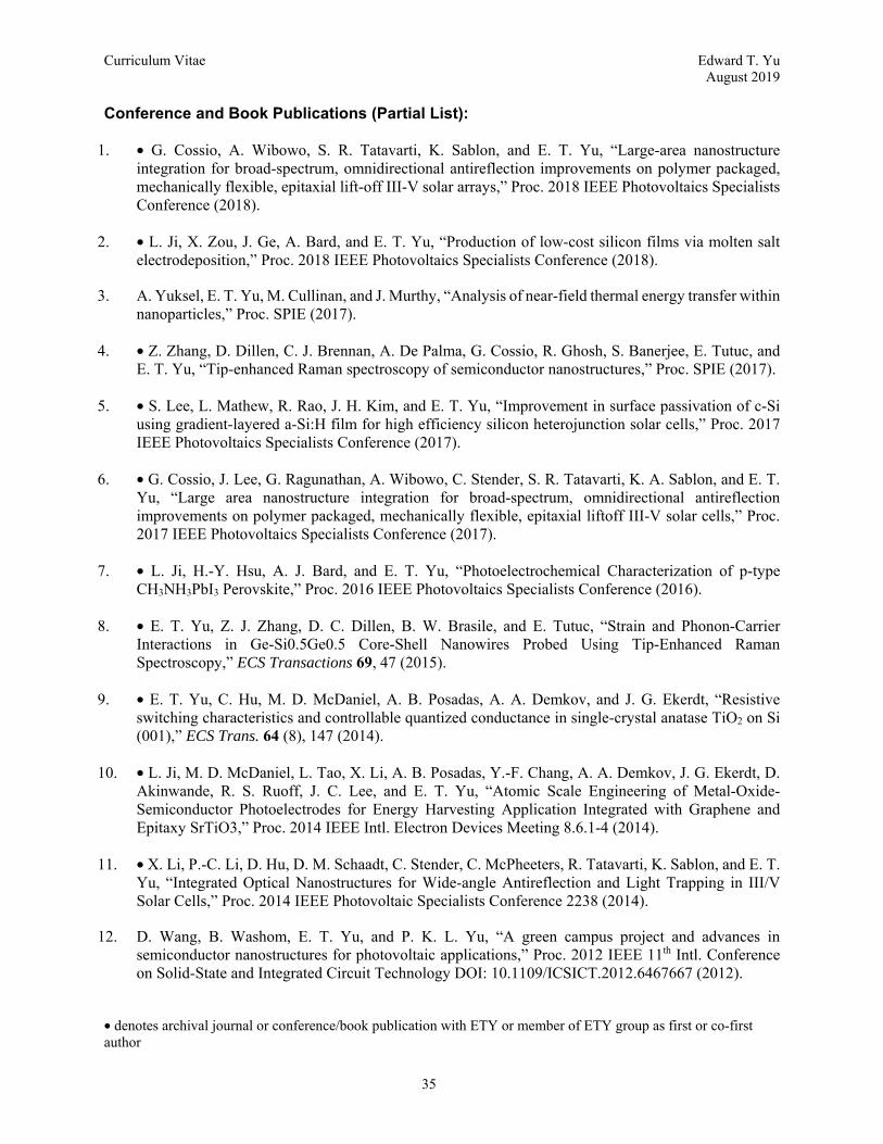
Curriculum Vitae Edward T. Yu August 2019
• denotes archival journal or conference/book publication with ETY or member of ETY group as first or co-first author
35
Conference and Book Publications (Partial List):
1. • G. Cossio, A. Wibowo, S. R. Tatavarti, K. Sablon, and E. T. Yu, “Large-area nanostructure integration for broad-spectrum, omnidirectional antireflection improvements on polymer packaged, mechanically flexible, epitaxial lift-off III-V solar arrays,” Proc. 2018 IEEE Photovoltaics Specialists Conference (2018).
2. • L. Ji, X. Zou, J. Ge, A. Bard, and E. T. Yu, “Production of low-cost silicon films via molten salt electrodeposition,” Proc. 2018 IEEE Photovoltaics Specialists Conference (2018).
3. A. Yuksel, E. T. Yu, M. Cullinan, and J. Murthy, “Analysis of near-field thermal energy transfer within nanoparticles,” Proc. SPIE (2017).
4. • Z. Zhang, D. Dillen, C. J. Brennan, A. De Palma, G. Cossio, R. Ghosh, S. Banerjee, E. Tutuc, and E. T. Yu, “Tip-enhanced Raman spectroscopy of semiconductor nanostructures,” Proc. SPIE (2017).
5. • S. Lee, L. Mathew, R. Rao, J. H. Kim, and E. T. Yu, “Improvement in surface passivation of c-Si using gradient-layered a-Si:H film for high efficiency silicon heterojunction solar cells,” Proc. 2017 IEEE Photovoltaics Specialists Conference (2017).
6. • G. Cossio, J. Lee, G. Ragunathan, A. Wibowo, C. Stender, S. R. Tatavarti, K. A. Sablon, and E. T. Yu, “Large area nanostructure integration for broad-spectrum, omnidirectional antireflection improvements on polymer packaged, mechanically flexible, epitaxial liftoff III-V solar cells,” Proc. 2017 IEEE Photovoltaics Specialists Conference (2017).
7. • L. Ji, H.-Y. Hsu, A. J. Bard, and E. T. Yu, “Photoelectrochemical Characterization of p-type CH3NH3PbI3 Perovskite,” Proc. 2016 IEEE Photovoltaics Specialists Conference (2016).
8. • E. T. Yu, Z. J. Zhang, D. C. Dillen, B. W. Brasile, and E. Tutuc, “Strain and Phonon-Carrier Interactions in Ge-Si0.5Ge0.5 Core-Shell Nanowires Probed Using Tip-Enhanced Raman Spectroscopy,” ECS Transactions 69, 47 (2015).
9. • E. T. Yu, C. Hu, M. D. McDaniel, A. B. Posadas, A. A. Demkov, and J. G. Ekerdt, “Resistive switching characteristics and controllable quantized conductance in single-crystal anatase TiO2 on Si (001),” ECS Trans. 64 (8), 147 (2014).
10. • L. Ji, M. D. McDaniel, L. Tao, X. Li, A. B. Posadas, Y.-F. Chang, A. A. Demkov, J. G. Ekerdt, D. Akinwande, R. S. Ruoff, J. C. Lee, and E. T. Yu, “Atomic Scale Engineering of Metal-Oxide-Semiconductor Photoelectrodes for Energy Harvesting Application Integrated with Graphene and Epitaxy SrTiO3,” Proc. 2014 IEEE Intl. Electron Devices Meeting 8.6.1-4 (2014).
11. • X. Li, P.-C. Li, D. Hu, D. M. Schaadt, C. Stender, C. McPheeters, R. Tatavarti, K. Sablon, and E. T. Yu, “Integrated Optical Nanostructures for Wide-angle Antireflection and Light Trapping in III/V Solar Cells,” Proc. 2014 IEEE Photovoltaic Specialists Conference 2238 (2014).
12. D. Wang, B. Washom, E. T. Yu, and P. K. L. Yu, “A green campus project and advances in semiconductor nanostructures for photovoltaic applications,” Proc. 2012 IEEE 11th Intl. Conference on Solid-State and Integrated Circuit Technology DOI: 10.1109/ICSICT.2012.6467667 (2012).

Curriculum Vitae Edward T. Yu August 2019
• denotes archival journal or conference/book publication with ETY or member of ETY group as first or co-first author
36
13. • C. O. McPheeters, D. Hu, X. Li, D. M. Schaadt, and E. T. Yu, “Performance benefits for thin-film solar cells incorporating semiconductor heterostructures and light trapping,” Proc. 2012 IEEE Photovoltaic Specialists Conference 444 (2012).
14. J. H. Yum, G. Bersuker, D. A. Ferrer, T. Akyol, M. Lei, K. W. Park, T. W. Hudnall, M. C. Downer, C. W. Bielawski, E. T. Yu, J. Price, P. Kirsch, R. Jammy, J. C. Lee, and S. K. Banerjee, “ALD beryllium oxide: novel barrier layer for high performance gate stacks on Si and high mobility substrates,” Proc. 2011 IEEE Int’l Electron Devices Meeting 28.2.1-4 (2011).
15. • E. T. Yu, “Engineering of plasmonic effects in photodetectors and high-efficiency photovoltaics,” Proc. 3rd Intl. Nanoelectronics Conference DOI: 10.1109/INEC.2010.5424447 (2010).
16. • C. O. McPheeters, C. J. Hill, D. Hu, S. H. Lim, D. Derkacs, D. Z. Ting, D. M. Schaadt, S. D. Gunapala, and E. T. Yu, “Toward high-efficiency quantum dot solar cells: optimized gratings for ultrathin waveguide devices,” Proc. SPIE 7772, 777209-1-7 (2010).
17. • D. Derkacs, W. V. Chen, P. Matheu, S. H. Lim, P. K. L. Yu, and E. T. Yu, “Coupling of light scattered by nanoparticles into waveguide modes in quantum-well solar cells,” Proc. SPIE 7047, 704703-1-10 (2008).
18. • E. T. Yu, D. Derkacs, S. H. Lim, P. Matheu, and D. M. Schaadt, “Plasmonic nanoparticle scattering for enhanced performance of photovoltaic and photodetector devices,” Proc. SPIE 7033, 70331V-1-9 (2008).
19. • J. J. M. Law, S. A. Dayeh, D. Wang, and E. T. Yu, “Scanning Capacitance Characterization of Potential Screening in InAs Nanowire Devices,” Proceedings of IEEE International Conference on Nanotechnology (2008).
20. • S. A. Dayeh, D. Susac, P. Chen, Y. Jing, K. L. Kavanagh, S. S. Lau, E. T. Yu, and D. Wang, “Optimal Control over the InAs Nanowire Growth for System Integration and their Structural and Transport Properties,” Proceedings of IEEE International Conference on Nanotechnology (2008).
21. • B. S. Simpkins, E. T. Yu, P. Waltereit, and J. S. Speck, “Distinguishing negatively-charged and highly conductive dislocations in gallium nitride using scanning Kelvin probe and conductive atomic force microscopy,” Mat. Res. Soc. Symp. Proc. 743, 35 (2003).
22. C. Wetzel, E. T. Yu, J. S. Speck, A. Rizzi, and Y. Arakawa, eds., GaN and Related Alloys – 2002 (Materials Research Society, 2003), xxi+862pp.
23. • E. T. Yu, “Spontaneous and piezoelectric polarization effects in nitride heterostructures,” in III-V Nitride Semiconductors: Applications and Devices, E. T. Yu and O. Manasreh, eds. (Taylor & Francis, 2003), pp. 161-191.
24. L. S. Yu and E. T. Yu, “Characterization of Schottky contacts on nitride semiconductors,” in III-V Nitride Semiconductors: Applications and Devices, E. T. Yu and O. Manasreh, eds. (Taylor & Francis, 2003), pp. 67-105.

Curriculum Vitae Edward T. Yu August 2019
• denotes archival journal or conference/book publication with ETY or member of ETY group as first or co-first author
37
25. L. Jia, D. Keogh, L. S. Yu, S. S. Lau, E. T. Yu, P. M. Asbeck, P. Miraglia, A. Roskowski, and R. F. Davis, “I-V characteristics of polarization-induced barriers in AlGaN/GaN heterostructures,” 2001 International Semiconductor Device Research Symposium Proceedings, p. 201 (2001).
26. • D. M. Schaadt and E. T. Yu, “Frequency response of trap states in an AlxGa1-xN/GaN heterostructure field-effect transistor measured at the nanoscale by dC/dV spectroscopy,” Mat. Res. Soc. Symp. Proc. 680E, E5.1.1 (2001).
27. • K. V. Smith and E. T. Yu, “Analysis of localized charge trapping behavior in AlGaN/GaN heterostructures,” Proceedings of the IEEE 27th International Symposium on Compound Semiconductors, 1 (2000).
28. • X. Z. Dang, P. M. Asbeck, E. T. Yu, K. S. Boutros, and J. M. Redwing, “Long time-constant trap effects in nitride heterostructure field-effect transistors,” Mat. Res. Soc. Symp. Proc. 622, T.28.1-6 (2000).
29. C. H. Yun, A. B. Wengrow, N. W. Cheung, Y. Zheng, R. J. Welty, Z. F. Guan, K. V. Smith, P. M. Asbeck, E. T. Yu, and S. S. Lau, “Ion-cut silicon layer transfer with patterned implantation of hydrogen,” Electrochemical Society Proceedings 99-3, 125 (1999).
30. C. C. Shi, P. M. Asbeck, and E. T. Yu, “Surface potential effects due to the piezoelectric charge associated with dislocations in GaN,” 41st Electronic Materials Conference Abstracts, p. 27 (1999).
31. • K. V. Smith, E. T. Yu, J. M. Redwing, and K. S. Boutros, “Local electronic structure of AlGaN/GaN heterostructures probed by scanning capacitance microscopy,” 41st Electronic Materials Conference Abstracts, p. 27 (1999).
32. • D. M. Schaadt, E. T. Yu, S. Sankar, and A. E. Berkowitz, “Nanoscale charge transport properties of Co/SiO2 multilayer structures and their application in a novel magnetic field sensor,” 41st Electronic Materials Conference Abstracts, p. 23 (1999).
33. • E. T. Yu, S. L. Zuo, and A. Y. Lew, “An atomic-scale view of semiconductor heterostructures using scanning tunneling microscopy (Invited),” Proceedings of the 5th International Conference on Solid-State and Integrated Circuit Technology, p. 657 (1998).
34. • E. T. Yu, X. Z. Dang, L. S. Yu, D. Qiao, P. M. Asbeck, S. S. Lau, G. J. Sullivan, K. S. Boutros, and J. M. Redwing, “Piezoelectric enhancement of Schottky barrier heights in GaN/AlGaN HFET structures,” 56th Annual Device Research Conference Digest, p. 116 (1998).
35. • P. A. Rosenthal, E. T. Yu, R. L. Pierson, and P. J. Zampardi, “Cross-sectional Kelvin probe force microscopy of epitaxial layers for heterojunction bipolar transistors,” 40th Electronic Materials Conference Abstracts, p. 6 (1998).
36. • X. Z. Dang, E. T. Yu, K. S. Boutros, and J. M. Redwing, “Characterization of defect levels in n-type Al0.15Ga0.85N/GaN heterostructures,” 40th Electronic Materials Conference Abstracts, p. 42 (1998).
37. • E. T. Yu, P. M. Asbeck, S. S. Lau, and G. J. Sullivan, “Piezoelectric Effects in AlGaN/GaN Heterostructure Field-Effect Transistors (Invited),” Electrochemical Society Proceedings 98-2, 468 (1998).

Curriculum Vitae Edward T. Yu August 2019
• denotes archival journal or conference/book publication with ETY or member of ETY group as first or co-first author
38
38. • E. T. Yu, “Nanoscale Characterization of Device Structures by Scanning Tunneling Microscopy (Invited),” 1997 Conference on Challenges in Predictive Process Simulation Meeting Abstracts, Tu-1910 (1997).
39. Q. Z. Liu, L. S. Yu, K. V. Smith, F. Deng, C. W. Tu, P. M. Asbeck, E. T. Yu, and S. S. Lau, “Metal-GaN Contact Technology (Invited),” Electrochemical Society Proceedings 97-34, 11 (1998).
40. Q. Z. Liu, K. V. Smith, E. T. Yu, S. S. Lau, N. R. Perkins, and T. F. Kuech, “On the Epitaxy of Metal Films on GaN,” Mat. Res. Soc. Symp. Proc. 449, 1079 (1997).
41. • A. Y. Lew, S. L. Zuo, E. T. Yu, and R. H. Miles, “Anisotropy in Atomic-Scale Interface Structure and Mobility in InAs/GaInSb Superlattices,” Mat. Res. Soc. Symp. Proc. 448, 147 (1997).
42. • A. Y. Lew, C. H. Yan, C. W. Tu, and E. T. Yu, “Investigation of Arsenide/Phosphide Heterostructures by Scanning Tunneling Microscopy,” Bull. Am. Phys. Soc. 40, 256 (1995).
43. • A. Y. Lew, E. T. Yu, D. H. Chow, and R. H. Miles, “Cross-Sectional Scanning Tunneling Microscopy of III-V Heterostructures Grown by Molecular-Beam Epitaxy,” Mat. Res. Soc. Symp. Proc. 340, 241 (1994).
44. M. B. Johnson, U. Maier, H. P. Meier, H. Salemink, E. T. Yu, and S. S. Iyer, “Atomic-Scale View of Epitaxial Layers with Cross-Sectional STM,” in Semiconductor Interfaces at the Sub-Nanometer Scale, ed. by H. W. M. Salemink and M. D. Pashley, Proceedings of the NATO Advanced Research Workshop on Physical Properties of Semiconductor Interfaces at Sub-Nanometer Scale, Riva del Garda, Italy (Kluwer Academic Publishers, The Netherlands, 1993).
45. R. M. Feenstra, A. Vaterlaus, E. T. Yu, P. D. Kirchner, C. L. Lin, J. M. Woodall, and G. D. Pettit, “Cross-Sectional Scanning Tunneling Microscopy of GaAs Doping Superlattices: Pinned vs. Unpinned Surfaces,” in Semiconductor Interfaces at the Sub-Nanometer Scale, ed. by H. W. M. Salemink and M. D. Pashley, Proceedings of the NATO Advanced Research Workshop on Physical Properties of Semiconductor Interfaces at Sub-Nanometer Scale, Riva del Garda, Italy (Kluwer Academic Publishers, The Netherlands, 1993) p. 127.
46. M. B. Johnson, H. W. M. Salemink, O. Albrektsen, and E. T. Yu, “Atomic Scale View of Epitaxial Layers with Cross-Sectional STM,” in Low-Dimensional Systems: New Concepts, Proceedings of the Seventh International Winter School, Mauterndorf, Austria (Springer-Verlag, New York, 1992), p. 108.
47. • E. T. Yu, Y. Rajakarunanayake, M. C. Phillips, J. O. McCaldin, and T. C. McGill, “Heterojunction Approaches to Light Emitters: The Role of Band Offsets,” Extended Abstracts of the 22nd Conference on Solid State Devices and Materials, Sendai, Japan (1990).
48. D. Z.-Y. Ting, E. T. Yu, D. A. Collins, D. H. Chow, and T. C. McGill, “Modeling InAs/GaSb/AlSb Interband Tunnel Structures,” in Computational Electronics: Semiconductor Transport and Device Simulation (Kluwer Academic Publishers, Dordrecht, Netherlands, 1991), p. 189.
49. D. A. Collins, D. H. Chow, E. T. Yu, D. Z.-Y. Ting, J. R. Soderstrom , Y. Rajakarunanayake, and T. C. McGill, “InAs/GaSb/AlSb: The Material System of Choice for Novel Tunneling Devices,” in Resonant Tunneling in Semiconductors, ed. by L. L. Chang and E. E. Mendez (Plenum Press, New York, 1991), p. 515 (1991).
Curriculum Vitae Edward T. Yu August 2019
• denotes archival journal or conference/book publication with ETY or member of ETY group as first or co-first author
39
50. D. Z.-Y. Ting, E. T. Yu, and T. C. McGill, “Theoretical Studies of Current Transport in Interband Tunnel Structures Using the Effective Bond Orbital Model,” 1990 International Electron Devices Meeting Technical Digest, 31.6.1 (1990).
51. D. H. Chow, J. R. Soderstrom, D. A. Collins, D. Z.-Y. Ting, E. T. Yu, and T. C. McGill, “Novel InAs/GaSb/AlSb Tunnel Structures,” in Quantum-Well and Superlattice Physics III, SPIE Vol. 1283 (Society of Photo-Optical Instrumentation Engineers, Bellingham, Washington, 1990), p. 2.
52. • E. T. Yu, M. C. Phillips, D. H. Chow, D. A. Collins, and T. C. McGill, “Measurement of Band Offsets in III-V/II-VI Semiconductor Heterostructures,” Bull. Am. Phys. Soc. 35, 416 (1990).
53. • E. T. Yu, E. T. Croke, T. C. McGill, and R. H. Miles, “Measurement of the Strain Dependence of the Si/Ge (100) Valence Band Offset,” in Growth of Semiconductor Structures and High Tc Thin Films on Semiconductors, SPIE Vol. 1285 (Society of Photo-Optical Instrumentation Engineers, Bellingham, Washington, 1990), p. 212.
Research Presentations of Edward T. Yu and Group (Partial List)
1. E. T. Yu, “Dielectric Polarization in Old and New Settings,” presentation at Harry H. Wieder Memorial Symposium, La Jolla, CA, August 2019. (Invited)
2. E. T. Yu, “Using Strain to Control Electronic Behavior in Atomically Thin Materials,” presentation at Jackson State University-UCSB PREM Materials Science Conference, Jackson, MS, July 2019. (Invited)
3. A. C. De Palma, G. Cossio, K. Jones, Q. Jiamin, X. Li, and E. T. Yu, “Photoluminescence Properties of MoS2 Under Large Strain Gradients,” presentation at 61st Electronic Materials Conference, Ann Arbor, MI, June 2019.
4. E. T. Yu, “Center for Dynamics and Control of Materials: an NSF MRSEC at UT Austin,” presentation/panel discussion at NSF Nanoscale Science and Engineering Grantees Conference, Alexandria, VA, December 2018. (Invited)
5. A. Yuksel, E. T. Yu, M. Cullinan, and J. Murthy, “Heat Transfer Modeling of Nanoparticle Packings on a Substrate,” presentation at ASME 2018 International Mechanical Engineering Congress and Exposition, Pittsburgh, PA, November 2018.
6. E. T. Yu, “Creating an Environment for Large-Scale, Interdisciplinary Research and Education – The Center for Dynamics and Control of Materials: an NSF MRSEC at UT Austin,” ECE Colloquium, University of Texas at Dallas, November 2018. (Invited)
7. E. T. Yu, “Center for Dynamics and Control of Materials: an NSF MRSEC at UT Austin,” presentation/panel discussion at Iberian Nanotechnology Laboratory (INL) Directors Forum, Braga, Portugal, October 2018. (Invited)
8. E. T. Yu, Z. J. Zhang, C. J. Brennan, A. C. De Palma, G. Cossio, and K. Koul, “Strain and electromechanical coupling at the nanoscale in atomically thin transition metal dichalcogenides,” presentation at Meeting of the Electrochemical Society, Cancun, Mexico, October 2018. (Invited)
Curriculum Vitae Edward T. Yu August 2019
40
9. A. Yuksel, E. T. Yu, M. Cullinan, and J. Murthy, “Effect of Interfacial Thermal Conductance Between the Nanoparticles,” presentation at ASME 2018 International Technical Conference and Exhibition on Packaging and Integration of Electronic and Photonic Microsystems, San Francisco, CA, August 2018.
10. A. C. De Palma, Z. J. Zhang, C. J. Brennan, K. Tran, Z. Dai, X. Li, N. Lu, and E. T. Yu, “Evolution of Raman modes of monolayer and multilayer WSe2 with strain,” presentation at 60th Electronic Materials Conference, Santa Barbara, CA, June 2018.
11. S. Muschinske, E. S. Walker, C. J. Brennan, Y. Sun, A. Yau, T. Trivedi, A. Roy, S. D. March, A. F. Briggs, E. M. Krivoy, D. Akinwande, M. L. Lee, E. T. Yu, and S. R. Bank, “Epitaxial growth and characterization of 2D Bi1-xSbx alloys on Si (111),” presentation at 60th Electronic Materials Conference, Santa Barbara, CA, June 2018.
12. G. Cossio, A. Wibowo, S. R. Tatavarti, K. Sablon, and E. T. Yu, “Large-area nanostructure integration for broad-spectrum, omnidirectional antireflection improvements on polymer packaged, mechanically flexible, epitaxial lift-off III-V solar arrays,” presentation at IEEE Photovoltaic Specialists Conference, Waikoloa, HI, June 2018.
13. L. Ji, X. Zou, J. Ge, A. Bard, and E. T. Yu, “Production of low-cost silicon films via molten salt electrodeposition,” presentation at IEEE Photovoltaic Specialists Conference, Waikoloa, HI, June 2018.
14. A. Yuksel, E. T. Yu, M. Cullinan, and J. Murthy, “Uncertainty Analysis of Near-Field Thermal Energy Transfer within Nanoparticle Packing,” presentation at 17th IEEE Intersociety Conference on Thermal and Thermomechanical Phenomena in Electronic Systems, San Diego, CA, May 2018.
15. D. A. Sanchez, Z. Dai, P. Wang, A. Cantu-Chavez, C. J. Brennan, E. T. Yu, R. Huang, and N. Lu, “Measuring and modeling liquid-filled nanobubbles trapped by 2D materials,” presentation at Conference on Physics and Chemistry of Semiconductor Interfaces (PCSI), Kona, HI, January 2018.
16. C. J. Brennan, K. Koul, N. Lu, and E. T. Yu, “Out-of-plane electromechanical response of transition metal dichalcogenides,” presentation at Conference on Physics and Chemistry of Semiconductor Interfaces (PCSI), Kona, HI, January 2018.
17. E. T. Yu, “Materials and Device Engineering at Small Spatial and Temporal Scales,” University of Texas ECE Colloquium, Austin, TX, October 2017. (Invited)
18. E. T. Yu, “Tip enhanced Raman spectroscopy of semiconductor nanostructures,” presentation at 2017 SPIE Optics and Photonics Conference, San Diego, CA, August 2017. (Invited)
19. A. Yuksel, M. Cullinan, E. T. Yu, and J. Y. Murthy, “Analysis of near-field thermal energy transfer within nanoparticles,” presentation at 2017 SPIE Optics and Photonics Conference, San Diego, CA, August 2017.
20. S. Lee, L. Mathew, R. Rao, J. H. Kim, and E. T. Yu, “Improvement in surface passivation of c-Si using gradient-layered a-Si:H film for high efficiency silicon heterojunction solar cells,” presentation at IEEE Photovoltaic Specialists Conference, Washington, DC, June 2017.
21. G. Cossio, J. Lee, G. Ragunathan, A. Wibowo, C. Stender, S. R. Tatavarti, K. A. Sablon, and E. T. Yu, “Large area nanostructure integration for broad-spectrum, omnidirectional antireflection

Curriculum Vitae Edward T. Yu August 2019
41
improvements on polymer packaged, mechanically flexible, epitaxial liftoff III-V solar cells,” presentation at IEEE Photovoltaic Specialists Conference, Washington, DC, June 2017.
22. Z. J. Zhang, C. J. Brennan, R. Ghosh, S. K. Banerjee, and E. T. Yu, “Tip-enhanced Raman spectroscopy of monolayer and bilayer MoS2,” presentation at 59th Electronic Materials Conference, South Bend, IN, June 2017.
23. C. J. Brennan, R. Ghosh, K. Koul, S. K. Banerjee, N. Lu, and E. T. Yu, “Probing out-of-plane electromechanical response and flexoelectricity of monolayer MoS2 using piezoresponse force microscopy,” presentation at 59th Electronic Materials Conference, South Bend, IN, June 2017.
24. E. S. Walker, C. J. Brennan, A. Roy, J. Damasco, S. D. March, A. F. Briggs, E. Davis, W. Zhu, D. Akinwande, N. Mason, E. T. Yu, and S. R. Bank, “Growth optimization of epitaxial bismuth thin films towards the 2D limit,” presentation at 59th Electronic Materials Conference, South Bend, IN, June 2017.
25. E. S. Walker, S. Muschinske, N. Yoon, C. J. Brennan, S. R. Na, S. D. March, Y. Sun, A. F. Briggs, E. Davis, D. Akinwande, M. L. Lee, K. J. Liechti, E. T. Yu, D. Wasserman, and S. R. Bank, “Epitaxial growth and transfer of Bi1-xSbx thin films,” presentation at 59th Electronic Materials Conference, South Bend, IN, June 2017.
26. C. Brennan, R. Ghosh, K. Koul, S. Banerjee, N. Lu, and E. T. Yu, “Electromechanical Response of Single and Few Layer MoS2 Using Piezoresponse Force Microscopy,” presentation at Fall Meeting of the Materials Research Society, Boston, MA, December 2016.
27. E. T. Yu, “Bandgap and conductivity engineering in metal-oxide-semiconductor water-splitting photoelectrodes,” presentation at ACS Symposium on Applications of Photonics in Energy and Life Sciences, Galveston, TX, November 2016. (Invited)
28. Z. J. Zhang, D. Dillen, E. Tutuc, and E. T. Yu, “Tip-enhanced Raman spectroscopy of electrically contacted Ge-SixGe1-x core-shell nanowires,” presentation at 58th Electronic Materials Conference, Newark, DE, June 2016.
29. L. Ji, H.-Y. Hsu, A. J. Bard, and E. T. Yu, “Photoelectrochemical characterization of p-type CH3NH3PbI3 perovskite,” presentation at IEEE Photovoltaic Specialists Conference, Portland, OR, June 2016.
30. E. T. Yu, “Imaging, electron transport, and energy harvesting using solid-state nanostructures,” ECE Department colloquium (Eleanore Hale Wilson Lecture), University of Minnesota, February 2016.
31. E. T. Yu, “Imaging and solar energy harvesting using solid-state nanostructures,” ECE Department seminar, Rice University, November 2015.
32. E. T. Yu, Z. J. Zhang, D. C. Dillen, and E. Tutuc, “Strain and phonon-carrier interactions in Ge-SixGe1-x core-shell nanowires probed using tip-enhanced Raman spectroscopy,” presentation at 228th Meeting of the Electrochemical Society, Phoenix, October 2015. (Invited)
33. E. T. Yu, C. Hu, M. D. McDaniel, A. B. Posadas, A. A. Demkov, and J. G. Ekerdt, “Epitaxial Oxides on Silicon for Resistive Switching Memories with Controllable Conductance Quantization,” presentation at CMOS Emerging Technologies Research Conference, Vancouver, Canada, May 2015. (Invited)

Curriculum Vitae Edward T. Yu August 2019
42
34. E. T. Yu, C. Hu, L. Ji, M. D. McDaniel, S. J. Wang, X. H. Li, H. Huang, A. B. Posadas, A. J. Bard, A. A. Demkov, J. G. Ekerdt, and J. C. Lee, “Exploiting nanoscale phenomena in epitaxial oxides grown on silicon,” presentation at KAUST Workshop on Functional Nanomaterials, Jeddah, Saudi Arabia, March 2015. (Invited)
35. L. Ji, M. McDaniel, L. Tao, X. Li, A. Posadas, Y.-F. Chang, A. Demkov, J. Ekerdt, D. Akinwande, R. Ruoff, J. Lee, and E. Yu, “Atomic Scale Engineering of Metal-Oxide-Semiconductor Photoelectrodes for Energy Harvesting Application Integrated with Graphene and Epitaxial SrTiO3,” presentation at 2014 IEEE International Electron Devices Meeting (IEDM), San Francisco, CA, December 2014.
36. C. Hu, M. D. McDaniel, A. B. Posadas, A. A. Demkov, J. G. Ekerdt, and E. T. Yu, “Resistive switching mechanism and controllable quantized conductance in single crystal TiO2 epitaxial oxides on Si (001),” presentation at Fall Meeting of the Materials Research Society, Boston, MA, December 2014.
37. X. Li, V. D. Dasika, P.-C. Li, L. Ji, S. R. Bank, and E. T. Yu, “Minimized reduction in open-circuit voltage for GaAs/InGaAs quantum well solar cells with bandgap-engineered graded quantum well depths,” presentation at 6th World Conference on Photovoltaic Energy Conversion, Kyoto, Japan, November 2014.
38. X. Li, P.-C. Li, C. Stender, R. Tatavarti, K. Sablon, and E. T. Yu, “Integrated optical nanostructures for wide angle antireflection and light trapping in III/V solar cells,” presentation at 6th World Conference on Photovoltaic Energy Conversion, Kyoto, Japan, November 2014.
39. E. T. Yu, C. Hu, M. D. McDaniel, A. B. Posadas, A. A. Demkov, and J. G. Ekerdt, “Resistive switching characteristics and controllable quantized conductance in single-crystal anatase TiO2 on Si (001),” presentation at 226th Meeting of the Electrochemical Society, Cancun, Mexico, October 2014. (Invited)
40. E. T. Yu, “Seeing (and using) the very small: imaging and solid-state device engineering at the nanoscale,” Materials Science & Engineering seminar, University of Texas at Austin, September 2014.
41. Z. Zhang, D. Dillen, E. Tutuc, and E. T. Yu, “Strain and hole gas induced Raman shifts in Ge-SixGe1-x core-shell nanowires using tip-enhanced Raman spectroscopy,” presentation at 56th Electronic Materials Conference, Santa Barbara, CA, June 2014.
42. V. D. Dasika, H. P. Nair, S. R. Bank, and E. T. Yu, “Raman spectroscopy investigation of nitrogen incorporation in GaSbN,” presentation at 56th Electronic Materials Conference, Santa Barbara, CA, June 2014.
43. L. Ji, Y.-F. Chang, B. Fowler, Y.-C. Chen, T.-M. Tsai, K.-C. Chang, M.-C. Chen, T.-C. Chang, S. M. Sze, E. T. Yu, and J. C. Lee, “Resistive Switching of SiOx with One Diode-One Resistor Nanopillar Architecture Fabricated via Nanosphere Lithography,” presentation at 72nd Device Research Conference, Santa Barbara, CA, June 2014.
44. X. Li, P.-C. Li, D. Hu, D. M. Schaadt, C. Stender, C. McPheeters, R. Tatavarti, K. Sablon, and E. T. Yu, “Integrated Optical Nanostructures for Wide-angle Antireflection and Light Trapping in III/V Solar Cells,” presentation at IEEE Photovoltaic Specialists Conference, Denver, CO, June 2014.

Curriculum Vitae Edward T. Yu August 2019
43
45. P. C. Li and E. T. Yu, “Large-Area, Flexible, Wavelength-Selective Three-Dimensional Optical Metasurface,” presentation at Spring Meeting of the Materials Research Society, San Francisco, CA, April 2014.
46. L. Ji, Y.-F. Chang, F. Zhou, F. Xue, B. Fowler, T.-M. Tsai, K.-C. Chang, T.-C. Chang, J. C. Lee, and E. T. Yu, “Study of SiOx-based resistive switching memory by nanosphere lithography,” presentation at Spring Meeting of the Materials Research Society, San Francisco, CA, April 2014.
47. Y.-F. Chang, L. Ji, F. Zhou, B. Fowler, E. T. Yu, and J. C. Lee, “High-density nano-pillar SiOx-based resistive switching memory using nano-sphere lithography to fabricate a one diode - one resistor 1D-1R architecture,” presentation at 21st International Symposium on VLSI Technology, Systems, and Applications, Hsinchu, Taiwan, April 2014.
48. L. Ji, M. D. McDaniel, S. Wang, A. Posadas, J. G. Ekerdt, A. A. Demkov, A. J. Bard, and E. T. Yu, “Efficient and stable photoelectrochemical water splitting with metal-insulator-semiconductor photoelectrodes grown by molecular beam epitaxy,” presentation at 41st Conference on Physics and Chemistry of Semiconductor Interfaces, Santa Fe, NM, January 2014.
49. Y.-F. Chang, L. Ji, P.-Y. Chen, F. Zhou, F. Xue, B. Fowler, E. T. Yu, and J. C. Lee, “Study of SiOx-based resistive switching memory by nanosphere lithography,” presentation at IEEE Semiconductor Interface Specialists Conference, Arlington, VA, December 2013.
50. K.W. Park, H.P. Nair, E.M. Krivoy, S.R. Bank, and E.T. Yu, “Thermal characterization of rare earth/III-V superlattice and nanocomposite structures using scanned probe microscopy,” presentation at 2013 Electronic Materials Conference, South Bend, IN, June 2013.
51. V.D. Dasika, E.M. Krivoy, H.P. Nair, S.J. Maddox, K.W. Park, D. Jung, M.L. Lee, E.T. Yu, and S.R. Bank, “InAs Quantum Dot Growth using Bismuth as a Surfactant for Optoelectronic Applications,” presentation at Conf. on Lasers and Electro Optics (CLEO), San Jose, CA, June 2013.
52. J. C. Chang, M. de Messieres, P. C. Li, O. I. Kulaeva, V. M. Studitsky, E. T. Yu, and A. La Porta, “Mechanical stability of mononucleosome revealed by optical torque wrench,” presentation at 57th Annual Meeting of the Biophysical Society, Philadelphia, PA, February 2013.
53. K. W. Park, H. P. Nair, S. R. Band, and E. T. Yu, “Proximal probe characterization of thermal conductivity in ErAs/GaAs superlattice grown by molecular beam epitaxy,” presentation at 40th Conference on Physics and Chemistry of Semiconductor Interfaces, Waikoloa, HI, January 2013.
54. D. Wang, B. Washom, E. T. Yu, and P. K. L. Yu, “A Green Campus project and advances in semiconductor nanostructures for photovoltaic applications,” presentation at IEEE International Conference on Solid-State and Integrated Circuit Technology,” Xian, China, October 2012. (Invited)
55. E. T. Yu, “Light trapping and quantum semiconductor structures for high efficiency photovoltaics,” presentation at IEEE Colloquium on Energy Harvesting Devices, College Park, MD, September 2012. (Invited)
56. E. T. Yu, “Photonic control and plasmonics for photovoltaics,” presentations at 2012 Inter-Continental Advanced Materials for Photonics Summer School on Renewable & Sustainable Energy, Boulder, CO, August 2012. (Invited)

Curriculum Vitae Edward T. Yu August 2019
44
57. V. D. Dasika, H. P. Nair, E. M. Krivoy, K. W. Park, E. T. Yu, and S. R. Bank, “InAs quantum dot growth using Bi as a surfactant,” presentation at 2012 Electronic Materials Conference, State College, PA, June 2012.
58. K. W. Park, V. D. Dasika, H. P. Nair, A. M. Crook, S. R. Bank, and E. T. Yu, “Scanned probe characterization of ErAs/GaAs nanostructures below the resolution limit via statistical analysis,” presentation at 2012 Electronic Materials Conference, State College, PA, June 2012.
59. P. C. Li and E. T. Yu, “Wide-angle wavelength selective optical metasurfaces,” presentation at 2012 Electronic Materials Conference, State College, PA, June 2012.
60. C. O. McPheeters, D. Hu, X. Li, D. M. Schaadt, and E. T. Yu, “Performance benefits for thin film solar cells incorporating semiconductor heterostructures and light trapping,” presentation at IEEE Photovoltaic Specialists Conference, Austin, TX, June 2012.
61. P. C. Li, Y. Zhao, A. Alu, and E. T. Yu, “Wide angle, wavelength-selective plasmonic multilayer metasurfaces,” presentation at 2012 Spring Meeting of the Materials Research Society, San Francisco, CA, April 2012.
62. E. T. Yu, C. O. McPheeters, X. Li, D. Hu, and D. M. Schaadt, “Quantum-well and quantum-dot structures for high-efficiency photovoltaics,” presentation at American Physical Society March Meeting, Boston, MA, February 2012. (Invited)
63. E. T. Yu, “Seeing the very small: imaging and solid-state device engineering at the nanoscale,” Electrical & Computer Engineering Department Colloquium, Texas Tech University, February 2012.
64. C. Hu, K. W. Park, A. Posadas, A. A. Demkov, and E. T. Yu, “Voltage-controlled magnetoresistance in a LaCoO3/SrTiO3 heterostructure,” presentation at 39th Conference on Physics and Chemistry of Semiconductor Interfaces, Santa Fe, NM, January 2012.
65. E. T. Yu, C. O. McPheeters, X. Li, D. Hu, and D. M. Schaadt, “Nanostructured III-V solar cells: light trapping and quantum semiconductor structures for high-efficiency photovoltaics,” presentation at NNIN Workshop on Materials and Manufacturing for Energy and Electronics, Austin, TX, January 2012. (Invited)
66. P. K. L. Yu, E. T. Yu, and D. Wang, “Advances in semiconductor nanostructures for photonic applications,” presentation at 20th International Symposium on Processing and Fabrication of Advanced Materials, Hong Kong, China, December 2011. (Invited)
67. E. T. Yu, “Light trapping and quantum semiconductor structures for high-efficiency photovoltaics,” presentation at OSA Conference on Optics for Solar Energy, Austin, TX, November 2011. (Invited)
68. H. Tang, P. Rannou, R. A. Mesch, L. Zhu, E. T. Yu, J. C. Lee, and C. G. Willson, “Mobility enhancement in mesophases of liquid crystalline organic semiconductors,” presentation at Organic Microelectronics and Optoelectronics Workshop VII, San Francisco, CA, July 2011.
69. E. T. Yu, C. O. McPheeters, D. Derkacs, and S. H. Lim, “Exploiting Nanostructure-based Scattering Effects in High-efficiency Photovoltaic Devices,” presentation at 2011 Spring Meeting of the Materials Research Society, San Francisco, CA, April 2011. (Invited)

Curriculum Vitae Edward T. Yu August 2019
45
70. E. T. Yu, C. O. McPheeters, and P. C. Li, “Exploiting interactions among metal, dielectric, and semiconductor nanostructures for photovoltaic devices,” presentation at 2011 Villa Conference on Interaction Among Nanostructures, Las Vegas, NV, April 2011. (Invited)
71. E. T. Yu, “Seeing the very small: imaging and solid-state device engineering at the nanoscale,” Materials Science & Engineering Department Colloquium, University of Texas at Dallas, April 2011.
72. E. T. Yu, “Exploiting plasmonic and nanostructure-based scattering effects for photovoltaic devices,” presentation at Lawrence Workshop on Epitaxy, Tempe, AZ, February 2011. (Invited)
73. K. W. Park, H. P. Nair, A. M. Crook, V. Dasika, S. R. Bank, and E. T. Yu, “Scanning probe microscopy studies of GaAs pn junctions with embedded ErAs nanoparticles,” presentation at 38th Conference on Physics and Chemistry of Semiconductor Interfaces, San Diego, CA, January 2011.
74. E. T. Yu, “Solid-state nanostructures for high-efficiency photovoltaics,” IEEE Distinguished Lecture, El Paso, TX, September 2010.
75. A. M. Crook, H. P. Nair, K. W. Park, E. T. Yu, and S. R. Bank, “Investigating the MBE overgrowth of semimetallic nanoparticles for nanophotonics,” presentation at 2010 North American Molecular-Beam Epitaxy Conference, Breckenridge, CO, September 2010.
76. H. P. Nair, A. M. Crook, K. W. Park, D. A. Ferrer, S. K. Banerjee, E. T. Yu, and S. R. Bank, “Investigation of MBE-grown ErAs nanoparticle morphology for high-performance optical and electronic devices,” presentation at 2010 North American Molecular-Beam Epitaxy Conference, Breckenridge, CO, September 2010.
77. C. O. McPheeters, C. J. Hill, D. Hu, S. H. Lim, D. Derkacs, D. Z. Ting, D. M. Schaadt, S. D. Gunapala, and E. T. Yu, “Toward high-efficiency quantum dot solar cells: optimized gratings for ultrathin waveguide devices,” presentation at 2010 SPIE Optics+Photonics Conference, San Diego, CA, August 2010.
78. A. Crook, H. Nair, K. W. Park, E. T. Yu, and S. R. Bank, “Overgrowth investigation of epitaxial semimetallic nanoparticles for photonic devices,” presentation at 52nd Electronic Materials Conference, Notre Dame, IN, June 2010.
79. K. W. Park, A. Crook, H. Nair, S. R. Bank, and E. T. Yu, “Scanned probe characterization of self-assembled ErAs/GaAs semimetal/semiconductor nanostructures grown by molecular-beam epitaxy,” presentation at 52nd Electronic Materials Conference, Notre Dame, IN, June 2010.
80. D. Z. Hu, C. O. McPheeters, E. T. Yu, and D. M. Schaadt, “Influence of monolayer AlAs on solar cells with InAs quantum dots embedded in InGaAs/GaAs matrix,” presentation at International Conference on Superlattices, Nanostructures, and Nanodevices (ICSNN-2010), Beijing, China, 2010.
81. P. Asbeck, L. Wang, S. Gu, Y. Taur, and E. T. Yu, “Tunneling MOSFET’s based on III-V staggered heterojunctions,” presentation at 2010 Spring MRS Meeting, San Francisco, CA, April 2010. (Invited)
82. E. T. Yu, “Engineering of plasmonic effects in photodetectors and high-efficiency photovoltaics,” presentation at 2010 IEEE International Nanoelectronics Conference, Hong Kong, China, January 2010. (Invited)

Curriculum Vitae Edward T. Yu August 2019
46
83. E. T. Yu, “Plasmonic and nanoparticle scattering effects in high-efficiency photovoltaics,” presentation at 2009 International Workshop on Physics of Semiconductor Devices, Delhi, India, December 2009. (Invited)
84. E. T. Yu, “Seeing the very small: imaging and solid-state device engineering at the nanoscale,” Department of Physics/IGERT seminar, University of Texas at Austin, Austin, TX, September 2009.
85. E. T. Yu, “New approaches for high-efficiency photovoltaics: solid-state device engineering at the nanoscale,” presentation at Applied Materials, Santa Clara, CA, July 2009.
86. J. J. M. Law, G. Koblmuller, F. Wu, J. S. Speck, and E. T. Yu, “Low dislocation-mediated reverse bias leakage in (0001) GaN via novel high-temperature MBE growth,” presentation at 51st Electronic Materials Conference, University Park, PA, June 2009.
87. E. T. Yu, “Seeing the very small: imaging and solid-state device engineering at the nanoscale,” Department of Electrical and Computer Engineering Distinguished Lecture Series, University of Texas, Austin, TX, April 2009.
88. E. T. Yu, “New technologies for solar energy harvesting: current reality and future potential,” presentation at La Jolla Research and Innovation Summit, La Jolla, CA, April 2009. (Invited)
89. E. T. Yu, “Exploiting nanoscale phenomena in solid-state devices: New concepts for energy and electronics,” Department of Physics seminar, University of California, Davis, CA, February 2009.
90. E. T. Yu, “Exploiting nanowires and nanoparticles for photovoltaics,” presentation at Workshop on Research Frontiers and Capability Gaps for Controlling and Designing Functional Materials, Los Alamos, NM, January 2009. (Invited)
91. L. Zhu and E. T. Yu, “Magnetoresistance amplification in a three-terminal ferromagnet/semiconductor spintronic device,” presentation at 36th Conference on Physics and Chemistry of Semiconductor Interfaces, Santa Barbara, CA, January 2009.
92. E. T. Yu, “Seeing the very small: imaging and solid-state device engineering at the nanoscale,” Department of Electrical and Computer Engineering seminar, University of Texas, Austin, TX, December 2008.
93. D. Derkacs, W. V. Chen, P. K. L. Yu, and E. T. Yu, “Improved performance of quantum well solar cells via nanoparticle light scattering,” presentation at Fall MRS Conference, Boston, MA, December 2008.
94. E. T. Yu, D. Derkacs, W. V. Chen, and P. K. L. Yu, “Plasmonic scattering enhancement of quantum-well solar cells,” presentation at 2008 OSA Frontiers in Optics Conference, Rochester, NY, October 2008. (Invited)
95. E. T. Yu, “Seeing the very small: imaging and solid-state device engineering at the nanoscale,” presentation at Korea University workshop on materials science and engineering, Seoul, Korea, August 2008. (Invited)
96. E. T. Yu, D. Derkacs, W. V. Chen, and P. K. L. Yu, “Quantum well and plasmonic nanostructures for high-efficiency photovoltaics,” presentation at 2008 SPIE Optics+Photonics Conference, San Diego, CA, August 2008. (Invited)

Curriculum Vitae Edward T. Yu August 2019
47
97. E. T. Yu, D. Derkacs, S. H. Lim, P. Matheu, D. M. Schaadt, W. V. Chen, and P. K. L. Yu, “Plasmonic nanoparticle scattering for enhanced performance of photovoltaic and photodetector devices,” presentation at 2008 SPIE Optics+Photonics Conference, San Diego, CA, August 2008. (Invited)
98. S. A. Dayeh, D. Susac, P. Chen, Y. Jing, K. Kavanagh, E. T. Yu, and D. Wang, “Optimal control over the InAs nanowire growth for system integration and their structural and transport properties,” presentation at 8th International Conference on Nanotechnology (2008 IEEE NANO), Arlington, TX, August 2008.
99. J. Law, S. Dayeh, D. Wang, and E. T. Yu, “Scanning capacitance characterization of potential screening in InAs nanowire devices,” presentation at 8th International Conference on Nanotechnology (2008 IEEE NANO), Arlington, TX, August 2008.
100. D. Z. Hu, C. McPheeters, E. T. Yu, and D. M. Schaadt, “Enhanced optical absorption via excitation of surface plasmon resonances in metal nanoparticles placed on a semiconductor device,” presentation at Summer School on Plasmonics, Porquorolles Island, France, 2008.
101. S. Dayeh, D. Susac, K. Kavanagh, E. T. Yu, and D. Wang, “Structural and electronic properties of zincblende and wurtzite InAs nanowires,” presentation at 2008 Electronic Materials Conference, Santa Barbara, CA, June 2008.
102. J. Law, S. Dayeh, D. Wang, and E. T. Yu, “Scanning capacitance characterization of potential screening in InAs nanowires,” presentation at 2008 Electronic Materials Conference, Santa Barbara, CA, June 2008.
103. S. A. Dayeh, Y. Jing, P. Chen, E. T. Yu, D. Wang, and S. S. Lau, “Integration of vertically and electrically isolated III-V nanowires on silicon,” presentation at 2008 Spring MRS Meeting, San Francisco, CA, April 2008.
104. S. A. Dayeh, S. M. Eichfeld, Y. Jing, P. Chen, E. T. Yu, D. Wang, J. M. Redwing, and S. S. Lau, “Vertically-aligned Si nanowires on silicon on insulator,” presentation at 2008 Spring MRS Meeting, San Francisco, CA, April 2008.
105. E. T. Yu, “Exploiting nanoscale phenomena in solid-state devices: New concepts for energy and electronics,” presentation at UCSD Jacobs School of Engineering Corporate Affiliates Program Board Meeting, La Jolla, CA, February 2008.
106. S. A. Dayeh, D. Wang, and E. T. Yu, “Mechanistic studies and precise control of III-V nanowire growth,” presentation at 35th Conference on Physics and Chemistry of Semiconductor Interfaces, Santa Fe, NM, January 2008.
107. S. A. Dayeh, E. T. Yu, and D. Wang, “Room temperature electron transport properties in InAs nanowires,” presentation at 2007 MRS Fall Meeting, Boston, MA, November 2007.
108. S. A. Dayeh, E. T. Yu, and D. Wang, “Optimum control over the Vapor-Liquid-Solid nanowire morphology through surface kinetics,” presentation at 2007 MRS Fall Meeting, Boston, MA, November 2007.
109. S. A. Dayeh, P. K. L. Yu, E. T. Yu, and D. Wang, “III-V nanowire growth mechanisms: VLS or VSS,” presentation at 49th Electronic Materials Conference, Notre Dame, IN, June 2007.
Curriculum Vitae Edward T. Yu August 2019
48
110. E. T. Yu, D. Derkacs, S. H. Lim, W. Mar, P. Matheu, and D. M. Schaadt, “Increasing efficiency of photovoltaics via surface plasmon polariton scattering effects in metal nanoparticles,“ presentation at Nanotech 2007 Conference, Santa Clara, CA, May 2007. (Invited)
111. S. A. Dayeh, P. K. L. Yu, E. T. Yu, and D. Wang, “Field-, diameter-, and surface state-dependent transport behavior in semiconductor nanowires,” presentation at 2007 MRS Spring Meeting, San Francisco, CA, April 2007.
112. E. T. Yu, “Seeing the very small: nanoscience and nanotechnology in electronic devices,” Department Colloquium, Department of Physics, Arizona State University, Tempe, AZ, March 2007.
113. E. T. Yu, “Seeing the very small: nanoscience and nanotechnology in electronic devices,” seminar presentation, Department of Materials Science & Engineering, UCLA, January 2007.
114. S. A. Dayeh, C. Soci, P. K. L. Yu, D. Wang, and E. T. Yu, “Interface state effects on the transport properties of InAs nanowire field-effect transistors,” presentation at 34th Conference on Physics and Chemistry of Semiconductor Interfaces, Salt Lake City, UT, January 2007.
115. X. Zhou, S. A. Dayeh, D. Wang, and E. T. Yu, “Scanning gate microscopy characterization of InAs nanowires,” presentation at 34th Conference on Physics and Chemistry of Semiconductor Interfaces, Salt Lake City, UT, January 2007.
116. E. T. Yu, “Seeing the very small: nanoscience and nanotechnology in electronic devices,” seminar presentation, Department of Mechanical Engineering, Northwestern University, Evanston, IL, September 2006.
117. E. T. Yu, “Prospects for realization of electrically pumped Si lasers,” presentation at DSRC Summer Conference, San Diego, CA, July 2006.
118. R. D. Yang, X. Zhou, E. T. Yu, and A. C. Kummel, “Trap energy determination by analysis of isothermal gated space-charge-limited current in organic thin-film transistors,” presentation at 48th Electronic Materials Conference, University Park, PA, June 2006.
119. S. A. Dayeh, D. Aplin, E. T. Yu, P. K. L. Yu, and D. L. Wang, “Growth mechanism and optimization of InAs nanowires synthesized by OMVPE,” presentation at 48th Electronic Materials Conference, University Park, PA, June 2006.
120. E. T. Yu, “Batteries and portable communications – some perspectives from the ‘field’,” presentation at DSRC Workshop II on 100% Efficient Electronics, Arlington, VA, March 2006.
121. E. T. Yu, “Seeing the very small: nanoscience and nanotechnology in electronic devices,” seminar presentation, San Diego Chapter of IEEE, San Diego, CA, March 2006.
122. S. Raychaudhuri and E. T. Yu, “Calculation of critical dimensions in coherently strained coaxial nanowire heterostructures,” presentation at 33rd Conference on Physics and Chemistry of Semiconductor Interfaces, Cocoa Beach, FL, January 2006.
123. X. Zhou, S. A. Dayeh, D. Aplin, D. Wang, and E. T. Yu, “Scanned electrical probe characterization of carrier transport behavior in InAs nanowires,” presentation at 33rd Conference on Physics and Chemistry of Semiconductor Interfaces, Cocoa Beach, FL, January 2006.
Curriculum Vitae Edward T. Yu August 2019
49
124. R. D. Yang, X. Zhou, A. Sharoni, C. Colesniuc, J. Park, E. T. Yu, I. K. Schuller, and A. C. Kummel, “Impedance spectroscopy and scanning Kelvin probe microscopy studies of charge injection and transport in phthallocyanine thin films,” presentation at 2005 Fall Meeting of the Materials Research Society, Boston, MA, November 2005.
125. E. T. Yu, B. S. Simpkins, X. Zhou, H. Zhang, E. J. Miller, and D. M. Schaadt, “Nanoscale electronic structure of defects in nitride semiconductors imaged by scanned probe microscopy,” presentation at 11th International Conference on Defects – Recognition, Imaging, and Physics in Semiconductors (DRIP XI), Beijing, China, September 2005. (Invited)
126. E. T. Yu, “Research prospects in wide band gap semiconductors,” presentation at 2005 Defense Sciences Research Council Summer Conference, San Diego, CA, July 2005.
127. S. A. Dayeh, D. Aplin, X. Zhou, P. K. L. Yu, E. T. Yu, and D. Wang, “Synthesis and characterization of InAs nanowires,” presentation at 47th Electronic Materials Conference, Santa Barbara, CA, June 2005.
128. H. Zhang, E. J. Miller, and E. T. Yu, “Analysis of leakage current mechanisms in GaN and AlGaN/GaN Schottky diodes,” presentation at 47th Electronic Materials Conference, Santa Barbara, CA, June 2005.
129. E. T. Yu and X. Zhou, “Nanoscale imaging of electronic structure in InGaN/GaN quantum wells,” presentation at International Conference on Metallurgical Coatings and Thin Films, San Diego, CA, May 2005. (Invited)
130. X. Zhou, E. T. Yu, D. I. Florescu, J. C. Ramer, D. S. Lee, S. M. Ting, and E. A. Armour, and W. E. Quinn, “Imaging of monolayer fluctuations and In clustering in InGaN/GaN quantum wells by scanning capacitance microscopy,” presentation at 32nd Conference on Physics and Chemistry of Semiconductor Interfaces, Bozeman, MT, January 2005.
131. E. T. Yu, “Probing electronic materials and devices at the nanometer scale,” colloquium presentation at Department of Materials Science and Engineering, University of California at Irvine, December 2004.
132. X. Zhou, E. T. Yu, D. I. Florescu, J. C. Ramer, D. S. Lee, S. M. Ting, and E. A. Armour, “Nanoscale imaging of InGaN thickness fluctuations and In clustering in InGaN/GaN quantum-well structures using SCM,” presentation at 2004 Fall Meeting of the Materials Research Society, Boston, MA, November 2004.
133. E. T. Yu, “Characterization for next-generation electronics,” presentation at Next Generation Electronics Workshop, Adelphi, MD, November 2004. (Invited)
134. E. T. Yu, X. Zhou, D. I. Florescu, J. C. Ramer, D. S. Lee, and E. A. Armour, “Scanned probe characterization of nanoscale structure in InGaN/GaN quantum wells,” presentation at AFOSR Workshop on Nanoscale Issues in Nitride Semiconductors, Anchorage, AK, August 2004. (Invited)
135. X. Zhou, E. T. Yu, D. I. Florescu, J. C. Ramer, D. S. Lee, and E. A. Armour, “Capacitance-voltage and scanning probe studies of InGaN/GaN quantum-well structures,” presentation at 46th Electronic Materials Conference, Notre Dame, IN, June 2004.

Curriculum Vitae Edward T. Yu August 2019
50
136. E. T. Yu, B. S. Simpkins, P. Waltereit, and J. S. Speck, “Electrical properties of dislocations in MBE-grown n-GaN,” presentation at 2004 Workshop on Compound Semiconductor Materials and Devices (WOCSEMMAD), Pasadena, CA, February 2004.
137. E. T. Yu, “Probing electronic materials and devices at the nanometer scale,” colloquium presentation at Department of Electrical and Computer Engineering, University of California at Riverside, January 2004.
138. D. M. Schaadt, E. T. Yu, V. Vaithyanathan, and D. G. Schlom, “Nanoscale current transport in epitaxial SrTiO3 on n+-Si imaged with conductive atomic force microscopy,” presentation at 31st Conference on Physics and Chemistry of Semiconductor Interfaces, Kona, HI, January 2004.
139. H. Zhang, E. J. Miller, E. T. Yu, C. Poblenz, and J. S. Speck, “Capacitance-voltage measurement of polarization charge and conduction-band offset at the InxGa1-xN/GaN heterojunction interface,” presentation at 31st Conference on Physics and Chemistry of Semiconductor Interfaces, Kona, HI, January 2004.
140. E. T. Yu, “Defects and nanoscale electronic structure in nitride semiconductors,” seminar presentation at Raytheon RF Components, Andover, MA, December 2003.
141. E. T. Yu, E. J. Miller, D. M. Schaadt, and B. S. Simpkins, “Nanoscale characterization and mitigation of defects in nitride semiconductors,” presentation at 2003 International Symposium on Compound Semiconductors, San Diego, August 2003. (Invited)
142. E. T. Yu, E. J. Miller, D. M. Schaadt, and B. S. Simpkins, “From microscopic characterization to processes for defect mitigation in nitride semiconductors,” Tri-Services Workshop on Process Induced Defects in Wide Bandgap Semiconductors, Grants Pass, OR, August 2003. (Invited, received Outstanding Speaker Award)
143. E. T. Yu, B. S. Simpkins, E. J. Miller, and D. M. Schaadt, “Influence of dislocations on charge distributions and carrier transport in nitride semiconductors,” ONR Workshop on Extended Defects in Wide Gap Semiconductors II, Irvington, VA, July 2003. (Invited, received Outstanding Speaker Award)
144. B. S. Simpkins, E. T. Yu, U. Chowdhury, M. M. Wong, T. G. Zhu, D. W. Yoo, and R. D. Dupuis, “Local conductivity and surface potential measurements of Mg-doped p-GaN,” presentation at 45th Electronic Materials Conference, Salt Lake City, UT, June 2003.
145. E. T. Yu, “Probing electronic materials and devices at the nanometer scale,” seminar presentation at SPAWAR Systems Center, San Diego, May 2003.
146. J. P. McGuire, C. Ciuti, L. J. Sham, and E. T. Yu, “Spintronics of an InAs surface layer with ferromagnetic gates,” presentation at 2003 March Meeting of the American Physical Society, Austin, TX, March 2003.
147. E. T. Yu, E. J. Miller, D. M. Schaadt, and B. S. Simpkins, “Electronic properties of defects in GaN characterized by scanning probe microscopy,” ONR Workshop on Characterization of Defects in Wide Bandgap Semiconductors, Hawaii, March 2003. (Invited)
148. E. T. Yu, “Probing electronic materials and devices at the nanometer scale,” Materials Research Lecture at California Institute of Technology, Pasadena, CA, February 19, 2003.

Curriculum Vitae Edward T. Yu August 2019
51
149. B. S. Simpkins and E. T. Yu, “Influence of AlN buffer on electronic properties and dislocation microstructure of AlGaN/GaN grown by molecular-beam epitaxy on SiC,” presentation at 30th Conference on Physics and Chemistry of Semiconductor Interfaces, Salt Lake City, UT, January 2003.
150. B. S. Simpkins, E. T. Yu, P. Waltereit, and J. S. Speck, “Correlated scanning Kelvin probe and conducting atomic force microscopy studies of dislocations in gallium nitride,” presentation at 2002 Fall MRS Meeting, Boston, MA, December 2002.
151. E. T. Yu, “Probing electronic materials and devices at the nanometer scale,” seminar presentation at Department of Materials Science and Engineering, Carnegie Mellon University, September 13, 2002.
152. E. T. Yu, “Probing electronic materials and devices at the nanometer scale,” seminar presentation at National Renewable Energy Laboratory, Golden, CO, August 23, 2002.
153. E. J. Miller, D. M. Schaadt, C. W. McKinney, E. T. Yu, P. Waltereit, C. Poblenz, and J. S. Speck, “Reverse-bias leakage current reduction in GaN Schottky diodes by surface modification with an atomic force microscope,” presentation at the 44th Electronic Materials Conference, Santa Barbara, CA, June 27, 2002.
154. E. T. Yu, “Probing electronic materials and devices at the nanometer scale,” seminar presentation at Department of Materials Science and Engineering, Stanford University, May 17, 2002.
155. B. S. Simpkins and E. T. Yu, “Polarization effects and local electronic properties in nitride heterostructures,” seminar presentation at Raytheon RF Components, Andover, MA, April 29, 2002.
156. E. T. Yu, “Probing electronic materials and devices at the nanometer scale,” seminar presentation at Department of Electrical Engineering, Ohio State University, Columbus, OH, April 9, 2002.
157. E. T. Yu, E. J. Miller, and D. M. Schaadt, “Scanning probe characterization of nanoscale charge transport,” Workshop on Induced Collective Phenomena in Semiconductors, Indianapolis, IN, March 2002.
158. P. M. Asbeck, E. T. Yu, S. S. Lau, L. Jia, and L. S. Yu, “Leakage currents through potential barriers in nitride materials and influence of polarization effects,” presentation at ONR Workshop on Extended Defects in Wide Gap Semiconductors: Electrical and Optical Effects, Belize, January 2002. (Invited)
159. E. T. Yu, E. J. Miller, D. M. Schaadt, C. Poblenz, C. Elsass, and J. S. Speck, “Electrical properties of extended defects in nitride semiconductors characterized by scanning probe microscopy,” presentation at ONR Workshop on Extended Defects in Wide Gap Semiconductors: Electrical and Optical Effects, Belize, January 2002. (Invited)
160. E. J. Miller, E. T. Yu, C. Poblenz, C. R. Elsass, and J. S. Speck, “Direct measurement of the polarization charge in AlGaN/GaN heterostructures using capacitance-voltage carrier profiling,” presentation at 29th Conference on Physics and Chemistry of Semiconductor Interfaces, Santa Fe, NM, January 2002.
161. D. M. Schaadt and E. T. Yu, “Scanning capacitance spectroscopy of an AlxGa1-xN/GaN heterostructure field-effect transistor structure: analysis of probe tip effects,” presentation at 29th Conference on Physics and Chemistry of Semiconductor Interfaces, Santa Fe, NM, January 2002.

Curriculum Vitae Edward T. Yu August 2019
52
162. E. T. Yu, “Nanoscale engineered photonic structures as strategic materials for defense applications,” presentation at Institute for Defense Analyses, Arlington, VA, December 2001.
163. E. J. Miller, D. M. Schaadt, E. T. Yu, C. Poblenz, C. R. Elsass, P. Waltereit, and J. S. Speck, “Characterization and local passivation of reverse-bias leakage paths in an AlGaN/GaN heterostructure,” presentation at 2001 MRS Fall Meeting, Boston, December 2001.
164. E. T. Yu, D. M. Schaadt, and K. V. Smith, “Nanoscale characterization of nitride heterostructures by scanning capacitance microscopy,” presentation at ONR Workshop on Near-Surface Effects in Semiconductor Substrates, Kodiak, AK, August 2001. (Invited)
165. E. T. Yu, D. M. Schaadt, K. V. Smith, and E. J. Miller, “Scanning capacitance characterization of AlGaN/GaN heterostructures,” presentation at 2001 GaN Electronics Workshop, Santa Barbara, CA, May 2001. (Invited)
166. E. T. Yu, “Probing electronic materials and devices at the nanoscale,” seminar presentation at UCSD Department of Physics, La Jolla, CA, May 2001.
167. P. M. Asbeck, E. T. Yu, S. S. Lau, L. Jia, D. Keogh, D. Qiao, E. Miller, P. Miraglia, A. Roskowski, and R. F. Davis, “Polarization-induced energy barriers in electronic devices,” presentation at 2001 MRS Spring Meeting, San Francisco, April 2001. (Invited)
168. D. M. Schaadt, E. T. Yu, and J. M. Redwing, “Frequency response of trap states in an AlxGa1-xN/GaN heterostructure field-effect transistor measured at the nanoscale by dC/dV spectroscopy,” presentation at 2001 MRS Spring Meeting, San Francisco, April 2001.
169. E. J. Miller and E. T. Yu, “Influence of the dipole interaction energy on clustering in InGaN,” presentation at 2001 MRS Spring Meeting, San Francisco, April 2001.
170. D. M. Schaadt, E. J. Miller, E. T. Yu, and J. M. Redwing, “Quantitative analysis of nanoscale electronic properties in an AlxGa1-xN/GaN heterostructure field-effect transistor structure,” presentation at the 28th Conference on Physics and Chemistry of Semiconductor Interfaces, Orlando, FL, January 2001.
171. E. T. Yu et al., “Nanoscale electronic properties in nitride semiconductor heterostructures,” presentation at 2000 AVS National Symposium, Boston, MA (2000). (Invited)
172. E. T. Yu, “Characterization of local electronic properties in nitride semiconductors,” presentation at ONR Workshop on Polarization Effects on Semiconductors, Glacier National Park, MT (2000). (Invited)
173. E. T. Yu, K. V. Smith, D. M. Schaadt, E. J. Miller, and B. S. Simpkins, “Characterization of nanoscale electronic properties in nitride semiconductors,” presentation at 27th International Symposium on Compound Semiconductors, Monterey, CA (2000). (Invited)
174. E. T. Yu, “Polarization effects and nanoscale electronic properties in nitride semiconductors,” seminar presentation at Lucent Technologies Bell Laboratories, Murray Hill, NJ, July 2000.
175. D. M. Schaadt, E. T. Yu, S. Sankar, and A. E. Berkowitz, “Hybrid magnetoelectronic device for magnetic field sensing,” presentation at 2000 Symposium on Spin Electronics, Halle, Germany (2000).

Curriculum Vitae Edward T. Yu August 2019
53
176. E. T. Yu, “Polarization effects and nanoscale electronic properties in nitride semiconductors,” seminar presentation at Wright-Patterson Air Force Base, OH, June 2000.
177. E. T. Yu et al., “Charge trapping effects in AlGaN/GaN HEMT structures,” presentation at ONR/NRL Workshop on Traps in AlGaN/GaN HEMT’s, Washington, DC (2000). (Invited)
178. P. A. Rosenthal, E. T. Yu, and P. J. Zampardi, “Structural and electronic properties of AlGaAs/GaAs heterojunction bipolar transistors characterized using cross-sectional scanning force microscopy,” presentation at 2000 Electronic Materials Conference, Denver, CO (2000).
179. K. V. Smith, X. Z. Dang, E. T. Yu, J. M. Redwing, D. A. Keough, C. Elsass, B. Heying, and J. S. Speck, “Comparison of charge trapping effects in AlGaN/GaN heterostructures based on Al composition, doping and growth technique,” presentation at 2000 Electronic Materials Conference, Denver, CO (2000).
180. X. Z. Dang, P. M. Asbeck, E. T. Yu, G. J. Sullivan, K. S. Boutros, and J. M. Redwing, “Long time constant trap effects in AlGaN/GaN HFET’s,” presentation at 2000 MRS Spring Meeting, San Francisco (2000).
181. B. B. Maranville, A. Shapiro, F. Hellman, D. M. Schaadt, and E. T. Yu, “Perpendicular magnetic anisotropy of CoPt3 on vicinal substrates,” presentation G26.011 at 2000 March Meeting of the American Physical Society, Minneapolis, MN (2000).
182. K. V. Smith, E. T. Yu, K. S. Boutros, and J. M. Redwing, “Charging effects in AlGaN/GaN heterostructures probed using scanning capacitance microscopy,” presentation at the 27th Conference on Physics and Chemistry of Semiconductor Interfaces, Salt Lake City, January 2000.
183. E. T. Yu and S. L. Zuo, “STM studies of semiconductor alloy layer and interface structure at the atomic scale”, presentation at 1999 MRS Fall Meeting, Boston (1999). (Invited)
184. E. T. Yu, K. V. Smith, X. Dang, P. M. Asbeck, and S. S. Lau, “Polarization effects and nanoscale electronic properties in nitride semiconductor heterostructures,” presentation at 1999 MRS Fall Meeting, Boston (1999). (Invited)
185. D. M. Schaadt, E. T. Yu, S. Sankar, and A. E. Berkowitz, “Novel hybrid magnetoelectronic device for magnetic field sensing,” presentation at 1999 National Symposium of the American Vacuum Society, Seattle, October 1999.
186. E. T. Yu, “Probing materials and devices at the atomic scale,” seminar presentation at VTT Electronics Laboratory, Espoo, Finland, Spetember 1999.
187. E. T. Yu, “Probing materials and devices at the atomic scale,” presentation at the TEKES Nanotechnology Workshop, Helsinki, Finland, September 1999. (Invited)
188. P. M. Asbeck, E. T. Yu, S. S. Lau, and W. Sun, “Vertical Transistors Implemented with GaN-Based Materials: Prospects and Progress,” presentation at XXVIth General Assembly of the International Union of Radio Science, Toronto, Canada, August 1999. (Invited)
189. K. V. Smith, E. T. Yu, J. M. Redwing, and K. S. Boutros, “Local electronic structure of AlGaN/GaN heterostructures probed by scanning capacitance microscopy,” presentation at 1999 Electronic Materials Conference, Santa Barbara, CA, July 1999.

Curriculum Vitae Edward T. Yu August 2019
54
190. D. M. Schaadt, E. T. Yu, S. Sankar, and A. E. Berkowitz, “Nanoscale charge transport properties of Co/SiO2 multilayer structures and their application in a novel magnetic field sensor,” presentation at 1999 Electronic Materials Conference, Santa Barbara, CA, July 1999.
191. C. C. Shi, P. M. Asbeck, and E. T. Yu, “Surface potential effects due to the piezoelectric charge associated with dislocations in GaN,” presentation at 1999 Electronic Materials Conference, Santa Barbara, CA, July 1999.
192. D. M. Schaadt, E. T. Yu, S. Sankar, and A. E. Berkowitz, “Charging and discharging of Co/SiO2 multilayer structures investigated by scanning force microscopy,” presentation at 1999 Spring MRS Meeting, San Francisco, April 1999.
193. Y. Zheng, Z. F. Guan, R. J. Welty, K. V. Smith, P. M. Asbeck, E. T. Yu, S. S. Lau, T. Hoechbauer, R. D. Verda, M. Nastasi, T. E. Haynes, C. H. Yun, A. B. Wengrow, and N. W. Cheung, “Patterned ion-cut techniques for semiconductors,” presentation at 1999 Spring MRS Meeting, San Francisco, April 1999.
194. E. T. Yu, “Probing electronic materials and device structures at the nanometer scale,” seminar presentation at California Institute of Technology, 14 April 1999.
195. E. T. Yu, “Probing electronic materials and device structures at the atomic scale,” seminar presentation at Stanford University, 18 March 1999.
196. E. T. Yu, “Polarization effects in III-V nitride heterostructure materials and device engineering,” seminar presentation at HP Labs, Palo Alto, CA, 19 March 1999.
197. E. T. Yu, “Probing electronic materials and device structures at the atomic scale,” seminar presentation at University of California at Berkeley, 5 March 1999.
198. E. T. Yu, “Polarization effects in III-V nitride heterostructure materials and device engineering,” seminar presentation at Stanford University, 4 March 1999.
199. E. T. Yu, “Spontaneous and piezoelectric polarization effects in III-V nitride heterostructures,” seminar presentation at Xerox Palo Alto Research Center (PARC), 26 February 1999.
200. E. T. Yu, “Probing electronic materials and device structures at the atomic slale,” seminar presentation at Jet Propulsion Laboratory, Pasadena, CA, 2 February 1999.
201. E. T. Yu, “Probing electronic materials and device structures at the atomic scale,” Laboratory Colloquium at HRL Laboratories, Malibu, CA, 28 January 1999.
202. P. M. Asbeck, E. T. Yu, S. S. Lau, and W. Sun, “Enhancement of base conductivity via the piezoelectric effect in AlGaN/GaN heterostructure bipolar transistors,” presentation at the Workshop on Wide Bandgap Bipolar Devices, Panama City Beach, FL, January 1999.
203. E. T. Yu, “Spontaneous and piezoelectric polarization effects in III-V nitride heterostructures,” presented at 1999 Conference on Physics and Chemistry of Semiconductor Interfaces, San Diego, January 1999. (Invited)

Curriculum Vitae Edward T. Yu August 2019
55
204. S. L. Zuo, E. T. Yu, A. A. Allerman, and R. M. Biefeld, “Cross-sectional scanning tunneling microscopy of InAsSb/InAsP superlattices,” presented at the 1999 Conference on Physics and Chemistry of Semiconductor Interfaces, San Diego, January 1999.
205. E. T. Yu, “Probing electronic materials and device structures at the atomic scale,” Department of Materials Science and Engineering Colloquium, UCLA, November 1998.
206. E. T. Yu, “Probing electronic materials and device structures at the atomic scale,” Department of Physics Condensed Matter Seminar, UCSD, November 1998.
207. X. Z. Dang, P. M. Asbeck, E. T. Yu, G. J. Sullivan, M. Y. Chen, B. T. McDermott, and K. S. Boutros, “Drift mobility in AlGaN/GaN heterostructure field-effect transistors,” presentation at the 1998 Materials Research Society Fall Meeting, Boston, December 1998.
208. E. T. Yu, “Cross-sectional scanning tunneling microscopy of InAs/GaInSb and InAsP/InAsSb superlattices for infrared applications,” presented at the Second Workshop on Characterization, Future Opportunities and Applications of 6.1Å III-V Semiconductors, Washington, DC, August 1998. (Invited)
209. E. T. Yu, “Nanoscale characterization of materials and devices by scanning probe techniques,” presented at US-Finland Workshop on Microstructuring Science and Technology, Espoo, Finland, August 1998. (Invited)
210. E. T. Yu, X. Z. Dang, L. S. Yu, D. Qiao, P. M. Asbeck, S. S. Lau, G. J. Sullivan, K. S. Boutros, and J. M. Redwing, “Piezoelectric enhancement of Schottky barrier heights in GaN/AlGaN HFET structures,” presented at the 1998 Device Research Conference, Charlottesville, VA, June 1998.
211. X. Z. Dang, E. T. Yu, K. S. Boutros, and J. M. Redwing, “Characterization of defect levels in n-type Al0.15Ga0.85N/GaN heterostructures,” presented at the Electronic Materials Conference, Charlottesville, VA, June 1998.
212. P. A. Rosenthal, E. T. Yu, R. L. Pierson, and P. J. Zampardi, “Cross-sectional Kelvin probe force microscopy of epitaxial layers for heterojunction bipolar transistors,” presented at Electronic Materials Conference, Charlottesville, VA, June 1998.
213. E. T. Yu, “Atomic-Scale Characterization of Semiconductor Heterostructures,” presented at 1998 National Symposium of the American Vacuum Society, Baltimore, November 1998. (Invited)
214. E. T. Yu, “STM Studies of Atomic-Scale Properties of Semiconductor Heterostructures,” presented at ICSICT ’98, Beijing, China, October 1998. (Invited)
215. E. T. Yu, “Cross-Sectional Scanning Tunneling Microscopy of Semiconductor Heterostructures,” presented at the 1998 Workshop on New Trends and Developments in Surface Science and Scanning Probe Microscopy, San Francisco, CA, May 29, 1998. (Invited)
216. S. L. Zuo, W. G. Bi, C. W. Tu, E. T. Yu, A. A. Allerman, and R. M. Biefeld, “Scanning tunneling microscopy of InAsP/InP and InAsP/InAsSb heterostructures,” presented at the 1998 Spring Meeting of the Materials Research Society, San Francisco, CA (1998).

Curriculum Vitae Edward T. Yu August 2019
56
217. E. T. Yu, P. M. Asbeck, X. Z. Dang, L. S. Yu, D. Qiao, S. S. Lau, and G. J. Sullivan, “Piezoelectric effects in GaN/AlGaN heterostructure field effect transistors,” presented at the 28th State-of-the-Art Program on Compound Semiconductors, San Diego, CA (1998). (Invited)
218. S. L. Zuo, W. G. Bi, C. W. Tu, and E. T. Yu, “Atomic Scale Compositional Structure of InAsP/InP Heterostructures Grown by Molecular-Beam Epitaxy,” presented at the 1998 Conference on Physics and Chemistry of Semiconductor Interfaces (1998).
219. E. T. Yu, “Atomic Scale Characterization of Semiconductor Heterostructures and Devices,” seminar presentation at Sandia National Laboratories, 14 January 1998.
220. E. T. Yu, “Atomic Scale Characterization of Semiconductor Heterostructures and Devices,” Materials Research Lecture seminar presentation at California Institute of Technology, 19 November 1997.
221. E. T. Yu, S. L. Zuo, A. Y. Lew, R. H. Miles, W. G. Bi, and C. W. Tu, “Atomic-Scale Properties of Semiconductor Heterostructures Probed by Scanning Tunneling Microscopy,” presented at 9th CIMTEC – World Ceramics Congress and Forum on New Materials, Florence, Italy, June 1998. (Invited)
222. E. T. Yu, S. L. Zuo, A. Y. Lew, W. G. Bi, and C. W. Tu, “Atomic-Scale Characterization by Cross-Sectional Scanning Tunneling Microscopy,” presented at 1998 ICMCTF, San Diego, CA, Spring 1998. (Invited)
223. B. L. Stein, E. T. Yu, E. T. Croke, A. T. Hunter, T. Laursen, A. E. Bair, J. W. Mayer, and C. C. Ahn, “Electronic Properties of Si/Si1–x–yGexCy Heterojunctions,” presented at the 2nd International Symposium on Silicon Heterostructures: from Physics to Devices, Barga, Italy, September 1997 (1997).
224. Q. Z. Liu, L. S. Yu, K. V. Smith, D. Qiao, C. D. Wang, C. W. Tu, P. M. Asbeck, E. T. Yu, and S. S. Lau, “Metal-GaN Contact Technology,” presented at 1997 International Meeting of The Electrochemical Society, Paris, France, September 1997 (1997). (Invited)
225. P. M. Asbeck, G. J. Sullivan, E. T. Yu, S. S. Lau, and B. McDermott, “Role of the Piezoelectric Effect in AlGaN/GaN HFET Behavior,” presented at the 1997 Device Research Conference, Ft. Collins, CO (1997).
226. E. T. Yu, “Cross-Sectional Scanning Tunneling Microscopy for Nanoscale Characterization of ULSI Devices,” presented at 1997 Conference on Challenges in Predictive Process Simulation, Wandlitz, Germany, August 1997 (1997). (Invited)
227. E. T. Yu, “Electronic Properties of Si/SiGeC Heterostructures,” presented at the Bohmische Physical Society Symposium, Tempe, AZ, June 1997 (1997). (Invited)
228. E. T. Yu, A. Y. Lew, S. L. Zuo, D. H. Chow, R. H. Miles, and Y.-H. Zhang, “Atomic-Scale Structure of Semiconductor Interfaces and Alloy Layers Studied by Scanning Tunneling Microscopy,” presented at the 1997 Scanning Microscopy Conference, Chicago, IL (1997). (Invited)
229. E. T. Yu, “Band Offsets in Si/SiGeC Heterojunctions,” invited presentation/discussion leader, Workshop on Growth and Device Applications of SiGeC Alloys, Austin, TX, April 1997 (1997). (Invited)

Curriculum Vitae Edward T. Yu August 2019
57
230. E. T. Yu, “Cross-Sectional Scanning Tunneling Microscopy of Semiconductor Heterostructures and Devices,” seminar presentation at University of Texas at Austin, April 1997 (1997).
231. B. L. Stein, E. T. Yu, E. T. Croke, A. T. Hunter, T. Laursen, A. E. Bair, J. W. Mayer, and C. C. Ahn, “Measurement of Band Offsets in Si/Si1–xGex and Si/Si1–x–yGexCy Heterojunctions,” presented at the 1997 Conference on Physics and Chemistry of Semiconductor Interfaces, Research Triangle Park, NC, (1997).
232. Q. Z. Liu, K. V. Smith, E. T. Yu, S. S. Lau, N. R. Perkins, and T. F. Kuech, “On the Epitaxy of Metal Films on GaN,” presented at the 1996 Materials Research Society Fall Meeting, Boston, MA (1996).
233. A. Y. Lew, S. L. Zuo, E. T. Yu, and R. H. Miles, “Anisotropy in Atomic-Scale Interface Structure and Mobility in InAs/GaInSb Superlattices,” presented at the 1996 Materials Research Society Fall Meeting, Boston, MA (1996).
234. Y.-H. Zhang, A. Y. Lew, E. T. Yu, and Y. Chen, “Microstructure Properties of InAs/InAs1–xSbx Superlattices and InAs1–xSbx Ordered Alloys Grown by Modulated Molecular Beam Epitaxy,” presented at the 1996 International Conference on Molecular-Beam Epitaxy, Malibu, CA (1996).
235. E. T. Yu, “Atomic-Scale Characterization of Semiconductor Heterostructures and Devices,” presented at 1996 Defense Sciences Research Council Summer Conference, La Jolla, CA, July 1996 (1996). (Invited)
236. B. L. Stein, E. T. Yu, E. T. Croke, A. T. Hunter, T. Laursen, A. E. Bair, J. W. Mayer, and C. C. Ahn, “Band Offsets in Si/Si1–x–yGexCy Heterojunctions Measured by Admittance Spectroscopy,” presented at the 1996 Electronic Materials Conference, Santa Barbara, CA (1996).
237. A. Y. Lew, E. T. Yu, and Y.-H. Zhang, “Atomic-Scale Structure of InAs/InAsSb Superlattices Grown by Modulated Molecular-Beam Epitaxy,” presented at the 1996 Conference on Physics and Chemistry of Semiconductor Interfaces, La Jolla, CA (1996).
238. E. T. Yu, “Cross-Sectional Scanning Tunneling Microscopy of Semiconductor Heterostructures and Devices,” seminar presentation at Stanford University, Stanford, CA, April 1996 (1996).
239. E. T. Yu, A. Y. Lew, R. B. Welstand, C. H. Yan, J. T. Zhu, C. W. Tu, P. K. L. Yu, D. H. Chow, R. H. Miles, and Y.-H. Zhang, “Cross-Sectional Scanning Tunneling Microscopy of Arsenide/Antimonide and Arsenide/Phosphide Semiconductor Heterostructures,” presented at the 1996 Materials Research Society Spring Meeting, San Francisco, CA (1996). (Invited)
240. C. H. Yan, A. Y. Lew, E. T. Yu, and C. W. Tu, “P2 Induced P/As Exchange on GaAs During Gas-Source Molecular-Beam Epitaxy Growth Interruption,” presented at the 1995 Conference on Chemical Beam Epitaxy, La Jolla, CA (1995).
241. E. T. Yu, “Cross-Sectional Scanning Tunneling Microscopy of Semiconductor Heterostructures and Devices,” seminar presentation at Hughes Research Laboratories, Malibu, CA, July 1995 (1995).
242. A. Y. Lew, C. H. Yan, C. W. Tu, and E. T. Yu, “Characterization of Arsenide/Phosphide Heterostructure Interfaces by Scanning Tunneling Microscopy,” presented at the 1995 International Conference on Formation of Semiconductor Interfaces, Princeton, NJ (1995).

Curriculum Vitae Edward T. Yu August 2019
58
243. A. Y. Lew, C. H. Yan, R. B. Welstand, J. T. Zhu, C. W. Tu, E. T. Yu, and P. K. L. Yu, “Interface Structure in Arsenide/Phosphide Heterostructures Grown by Gas-Source MBE and Low-Pressure MOVPE,” presented at the 1995 Electronic Materials Conference, Charlottesville, VA (1995).
244. A. Y. Lew, C. H. Yan, C. W. Tu, and E. T. Yu, “Investigation of Arsenide/Phosphide Heterostructures by Scanning Tunneling Microscopy,” presented at the 1995 American Physical Society March Meeting, San Jose, CA (1995).
245. E. T. Yu, “Cross-Sectional Scanning Tunneling Microscopy of Semiconductor Materials and Devices,” seminar presentation at University of California at Berkeley, February 1995 (1995).
246. E. T. Yu, “Cross-Sectional Scanning Tunneling Microscopy of Semiconductor Materials and Devices,” seminar presentation at Arizona State University, Tempe, AZ, November 1994 (1994).
247. A. Y. Lew, E. T. Yu, D. H. Chow, and R. H. Miles, “Cross-Sectional Scanning Tunneling Microscopy of InAs/GaInSb Superlattices,” presentation at 27th Annual Symposium of the Southern California Chapter of the American Vacuum Society, Pasadena, CA, September 1994 (1994).
248. E. T. Yu, “Atomic-Scale Imaging of Electronic and Optoelectronic Devices,” seminar presentation, Photonics Society of Chinese-Americans, San Diego, CA, July 1994 (1994).
249. E. T. Yu, “Cross-Sectional Scanning Tunneling Microscopy of Semiconductor Materials and Devices,” seminar presentation at University of California at Los Angeles, June 1994 (1994).
250. E. T. Yu, A. Y. Lew, D. H. Chow, R. H. Miles, and J. N. Schulman, “Interfacial Properties of InAs/GaInSb Superlattices Studied by Cross-Sectional STM,” presentation at the Engineering Foundation Conference on Surfaces and Interfaces in Mesoscopic Devices, Kona, HI, April 1994 (1994).
251. E. T. Yu, “Cross-Sectional Scanning Tunneling Microscopy of Semiconductor Materials and Devices,” seminar presentation at University of California at Santa Barbara, April 1994 (1994).
252. A. Y. Lew, E. T. Yu, D. H. Chow, and R. H. Miles, “Cross-Sectional Scanning Tunneling Microscopy of III-V Heterostructures Grown by Molecular-Beam Epitaxy,” presented at the 1994 Materials Research Society Spring Meeting, San Francisco, CA (1994).
253. M. W. Wang, J. F. Swenberg, R. J. Miles, M. C. Phillips, E. T. Yu, J. O. McCaldin, R. W. Grant, and T. C. McGill, “Measurement of the MgSe/Cd0.54Zn0.46Se Valence Band Offset by X-ray Photoelectron Spectroscopy,” presented at 6th International Conference on II-VI Compounds and Related Optoelectronic Materials, Newport, RI (1993).
254. E. T. Yu, A. Y. Lew, D. H. Chow, and R. H. Miles, “Cross-Sectional Scanning Tunneling Microscopy of InAs/GaInSb Infrared Superlattices,” presentation at 6.1Å Workshop, Santa Barbara, CA, December 1993 (1993).
255. E. T. Yu, “Electronic Profiling of Semiconductor Materials and Devices by Scanning Tunneling Microscopy,” seminar presentation at Naval Command, Control and Ocean Surveillance Center, San Diego, CA, April 1993 (1993).

Curriculum Vitae Edward T. Yu August 2019
59
256. E. T. Yu, “Electronic Profiling of Semiconductor Materials and Devices by Scanning Tunneling Microscopy,” seminar presentation at Hughes Technology Center, Carlsbad, CA, January 1993 (1993).
257. E. T. Yu, “Electronic Profiling of Semiconductor Devices by Scanning Tunneling Microscopy,” seminar presented at Department of Electrical and Computer Engineering, University of California, San Diego January 1993 (1993).
258. M. B. Johnson, U. Maier, H. P. Meier, H. Salemink, E. T. Yu, and S. S. Iyer, “Atomic-Scale View of Epitaxial Layers with Cross-Sectional STM,” presented at the NATO Advanced Research Workshop on Physical Properties of Semiconductor Interfaces at Sub-Nanometer Scale, Riva del Garda, Italy (1992).
259. R. M. Feenstra, A. Vaterlaus, E. T. Yu, P. D. Kirchner, C. L. Lin, J. M. Woodall, and G. D. Pettit, “Cross-Sectional Scanning Tunneling Microscopy of GaAs Doping Superlattices: Pinned vs. Unpinned Surfaces,” presented at the NATO Advanced Research Workshop on Physical Properties of Semiconductor Interfaces at Sub-Nanometer Scale, Riva del Garda, Italy (1992).
260. E. T. Yu, M. B. Johnson, A. R. Powell, J.-M. Halbout, and S. S. Iyer, “Scanning Tunneling Microscopy and Spectroscopy of Si-Based Heterostructures,” presented at the 1992 Symposium of the American Vacuum Society, Chicago, IL (1992).
261. E. T. Yu, M. B. Johnson, V. P. Kesan, J.-M. Halbout, and S. S. Iyer, “Cross-Sectional Scanning Tunneling Microscopy of MBE-Grown Si p-n Junctions and Si/SiGe Superlattices,” presented at the 1992 International Conference on Molecular-Beam Epitaxy, Schwäbisch Gmünd, Germany (1992).
262. E. T. Yu, “Electronic Profiling of Semiconductor Materials and Devices by Scanning Tunneling Microscopy,” seminar presented at California Institute of Technology, Pasadena, CA, July 1992 (1992).
263. E. T. Yu, “Electronic Profiling of Semiconductor Devices by Scanning Tunneling Microscopy,” seminar presented at Hughes Research Laboratories, Malibu, CA, June 1992 (1992).
264. M. B. Johnson, H. W. M. Salemink, O. Albrektsen, and E. T. Yu, “Atomic Scale View of Epitaxial Layers with Cross-Sectional STM,” presented at the Seventh International Winter School, Mauterndorf, Austria (1992).
265. E. T. Yu, M. C. Phillips, M. W. Wang, D. H. Chow, J. O. McCaldin, and T. C. McGill, “Measurement of the AlSb/ZnTe Valence Band Offset by X-Ray Photoelectron Spectroscopy,” presented at the 1991 Electronic Materials Conference, Boulder, CO (1991).
266. E. T. Yu, “Measurements of Heterojunction Band Offsets and Investigations of Novel Resonant Tunneling Structures,” seminar presented at Department of Electrical and Computer Engineering, University of California, San Diego, April 1991 (1991).
267. E. T. Yu, M. C. Phillips, J. O. McCaldin, and T. C. McGill, “Measurement of the CdSe/ZnTe Valence Band Offset by XPS,” presented at the 1991 Conference on Physics and Chemistry of Semiconductor Interfaces, Long Beach, CA (1991).

Curriculum Vitae Edward T. Yu August 2019
60
268. E. T. Yu, “Measurements of Heterojunction Band Offsets and Investigations of Novel Resonant Tunneling Structures,” seminar presented at General Electric Corporate Research and Development Center, February 1991 (1991).
269. E. T. Yu, “Measurements of Heterojunction Band Offsets and Investigations of Novel Resonant Tunneling Structures,” seminar presented at IBM T. J. Watson Research Center, February 1991 (1991).
270. D. Z.-Y. Ting, E. T. Yu, and T. C. McGill, “Band Structure Effects on Interband Tunnel Structures,” presented at the 1991 Conference on Physics and Chemistry of Semiconductor Interfaces, Long Beach, CA (1991).
271. D. Z.-Y. Ting, E. T. Yu, and T. C. McGill, “Theoretical Studies of Current Transport in Interband Tunnel Structures Using the Effective Bond Orbital Model,” presented at the 1990 International Electron Devices Meeting, San Francisco, CA (1990).
272. M. C. Phillips, E. T. Yu, Y. Rajakarunanayake, J. O. McCaldin, D. A. Collins, and T. C. McGill, “Characterization of CdSe/ZnTe Heterojunctions,” presented at the 1990 International Conference on Molecular-Beam Epitaxy, La Jolla, CA (1990).
273. E. T. Yu, Y. Rajakarunanayake, M. C. Phillips, J. O. McCaldin, and T. C. McGill, “Heterojunction Approaches to Light Emitters: The Role of Band Offsets,” presented at the 22nd Conference on Solid State Devices and Materials, Sendai, Japan (1990). (Invited)
274. D. A. Collins, D. Z.-Y. Ting, D. H. Chow, E. T. Yu, J. R. Soderstrom, Y. Rajakarunanayake, and T. C. McGill, “Interband Tunneling in InAs/GaSb/AlSb Heterostructures,” presented at the 1990 International Conference on Molecular-Beam Epitaxy, La Jolla, CA (1990).
275. D. Z.-Y. Ting, E. T. Yu, D. A. Collins, D. H. Chow, and T. C. McGill, “Modeling InAs/GaSb/AlSb Interband Tunnel Structures,” presented at the 1990 Workshop on Computational Electronics, Urbana, IL (1990).
276. D. A. Collins, D. H. Chow, E. T. Yu, D. Z.-Y. Ting, J. R. Soderstrom , Y. Rajakarunanayake, and T. C. McGill, “InAs/GaSb/AlSb: The Material System of Choice for Novel Tunneling Devices,” presented at the 1990 NATO Advanced Workshop on Resonant Tunneling in Semiconductors, El Escorial, Spain (1990).
277. E. T. Yu, M. C. Phillips, D. H. Chow, D. A. Collins, and T. C. McGill, “Measurement of Band Offsets in III-V/II-VI Semiconductor Heterostructures,” presented at the 1990 American Physical Society March Meeting, Anaheim, CA (1990).
278. E. T. Yu, E. T. Croke, D. H. Chow, D. A. Collins, M. C. Phillips, T. C. McGill, J. O. McCaldin, and R. H. Miles, “Measurement of the Valence Band Offset in Novel Heterojunction Systems: Si/Ge (100) and AlSb/ZnTe (100),” presented at the 1990 Conference on Physics and Chemistry of Semiconductor Intefaces, Clearwater, FL (1990).
279. D. Z.-Y. Ting, E. T. Yu, D. A. Collins, D. H. Chow, and T. C. McGill, “Modeling of Novel Heterojunction Tunnel Structures,” presented at the 1990 Conference on Physics and Chemistry of Semiconductor Intefaces, Clearwater, FL (1990).

Curriculum Vitae Edward T. Yu August 2019
61
280. E. T. Yu, E. T. Croke, T. C. McGill, and R. H. Miles, “Measurement of the Strain Dependence of the Si/Ge (100) Valence Band Offset,” presented at the 1990 SPIE Conference on Growth of Semiconductor Structures and High Tc Thin Films on Semiconductors, San Diego, CA (1990).
281. D. H. Chow, J. R. Soderstrom, D. A. Collins, D. Z.-Y. Ting, E. T. Yu, and T. C. McGill, “Novel InAs/GaSb/AlSb Tunnel Structures,” presented at the 1990 SPIE Conference on Quantum-Well and Superlattice Physics III, San Diego, CA (1990).
282. D. A. Collins, D. H. Chow, D. Z.-Y. Ting, E. T. Yu, J. R. Soderstrom, and T. C. McGill, “Large Peak-to-Valley Current Ratios in Triple Barrier Heterostructures,” presented at the 1989 Conference on Hot Carriers in Semiconductors, Phoenix, AZ (1989).
283. E. T. Yu, D. H. Chow, and T. C. McGill, “Commutativity of the GaAs/AlAs (100) Valence Band Offset,” presented at the 1988 Molecular-Beam Epitaxy Workshop, West Lafayette, IN (1988).

Curriculum Vitae Edward T. Yu August 2019
62
Professional References
Available upon request.