eden: enabling energy-efficient, high-performance deep ... · dnn with low energy, high...
TRANSCRIPT

EDEN: Enabling Energy-Efficient, High-PerformanceDeep Neural Network Inference Using Approximate DRAM
Skanda Koppula Lois Orosa A. Giray YağlıkçıRoknoddin Azizi Taha Shahroodi Konstantinos Kanellopoulos Onur Mutlu
ETH Zürich
ABSTRACTThe effectiveness of deep neural networks (DNN) in vision, speech,and language processing has prompted a tremendous demand forenergy-efficient high-performance DNN inference systems. Due tothe increasing memory intensity of most DNN workloads, mainmemory can dominate the system’s energy consumption and stalltime. One effective way to reduce the energy consumption andincrease the performance of DNN inference systems is by usingapproximate memory, which operates with reduced supply volt-age and reduced access latency parameters that violate standardspecifications. Using approximate memory reduces reliability, lead-ing to higher bit error rates. Fortunately, neural networks have anintrinsic capacity to tolerate increased bit errors. This can enableenergy-efficient and high-performance neural network inferenceusing approximate DRAM devices.
Based on this observation, we propose EDEN, the first generalframework that reduces DNN energy consumption and DNN eval-uation latency by using approximate DRAM devices, while strictlymeeting a user-specified target DNN accuracy. EDEN relies on twokey ideas: 1) retraining the DNN for a target approximate DRAMdevice to increase the DNN’s error tolerance, and 2) efficient map-ping of the error tolerance of each individual DNN data type to acorresponding approximate DRAM partition in a way that meetsthe user-specified DNN accuracy requirements.
We evaluate EDEN on multi-core CPUs, GPUs, and DNN accel-erators with error models obtained from real approximate DRAMdevices. We show that EDEN’s DNN retraining technique reliablyimproves the error resiliency of the DNN by an order of magnitude.For a target accuracy within 1% of the original DNN, our resultsshow that EDEN enables 1) an average DRAM energy reductionof 21%, 37%, 31%, and 32% in CPU, GPU, and two different DNNaccelerator architectures, respectively, across a variety of state-of-the-art networks, and 2) an average (maximum) speedup of 8% (17%)and 2.7% (5.5%) in CPU and GPU architectures, respectively, whenevaluating latency-bound neural networks.
CCS CONCEPTS• Computing methodologies → Neural networks; • Computersystems organization → Neural networks; Special purpose sys-tems; • Hardware → Dynamic memory.
KEYWORDSdeep neural networks, error tolerance, energy efficiency, machinelearning, DRAM, memory systems
Permission to make digital or hard copies of part or all of this work for personal orclassroom use is granted without fee provided that copies are not made or distributedfor profit or commercial advantage and that copies bear this notice and the full citationon the first page. Copyrights for third-party components of this work must be honored.For all other uses, contact the owner/author(s).MICRO-52, October 12–16, 2019, Columbus, OH, USA© 2019 Copyright held by the owner/author(s).ACM ISBN 978-1-4503-6938-1/19/10.https://doi.org/10.1145/3352460.3358280
ACM Reference Format:Skanda Koppula, Lois Orosa, A. Giray Yağlıkçı, Roknoddin Azizi, Taha Shah-roodi, Konstantinos Kanellopoulos, and Onur Mutlu. 2019. EDEN: EnablingEnergy-Efficient, High-Performance Deep Neural Network Inference UsingApproximate DRAM. In Proceedings of The 52nd Annual IEEE/ACM Interna-tional Symposium on Microarchitecture (MICRO-52). Columbus, OH, USA,October 12-16, 2019, 16 pages. https://doi.org/10.1145/3352460.3358280
1 INTRODUCTIONDeep neural networks (DNNs) [87, 90] are an effective solution tochallenges in computer vision, speech recognition, language trans-lation, drug discovery, robotics, particle physics, and a number ofother domains [9, 22, 41, 49, 50, 68, 84, 87, 102, 137, 149]. DNNsand their various flavors (convolutional neural networks [84], fully-connected neural networks [88], and recurrent neural networks[49]) are commonly evaluated in settings with edge devices thatdemand low energy and real-time responses [13, 146]. Unfortu-nately, DNNs have high computational and memory demands thatmake these energy and performance requirements difficult to fulfill.As such, neural networks have been the subject of many recentaccelerators and DNN-focused architectures. Recent works (e.g.,[6–8, 14, 25, 26, 29, 52, 54, 70, 100, 126, 152, 154, 158, 181]) focus onbuilding specialized architectures for efficient computation sched-uling and dataflow to execute DNNs [86, 109].
Improvements to accelerator efficiency [27, 85], DNN-optimizedGPU kernels [23, 28], and libraries designed to efficiently lever-age instruction set extensions [23, 83] have improved the compu-tational efficiency of DNN evaluation. However, improving thememory efficiency of DNN evaluation is an on-going challenge[13, 29, 37, 54, 107, 148]. The memory intensity of DNN inference isincreasing, and the sizes of state-of-art DNNs have grown dramati-cally in recent years. The winning model of the 2017 ILSVRC imagerecognition challenge [140], ResNeXt, contains 837M FP32 parame-ters (3.3 GB) [171]. This is 13.5x the parameter count of AlexNet,the winning model in 2012 [84]. More recent models have brokenthe one billion FP32 parameter mark (3.7 GB) [153]. As the machinelearning community trends towards larger, more expressive neuralnetworks, we expect off-chip memory problems to bottleneck DNNevaluation.
The focus of this work is to alleviate two main issues (energyand latency) of off-chip DRAM for neural network workloads. First,DRAM has high energy consumption. Prior works on DNN accelera-tors report that between 30 to 80% of system energy is consumed byDRAM [26, 99, 113, 130]. Second, DRAM has high latency. A load orstore that misses the last level cache (LLC) can take 100x longer timeto service compared to an L1 cache hit [32, 43, 44, 96, 114–116, 159].Prior work in accelerator design has targeted DRAM latency as achallenge for sparse and irregular DNN inference [165].
To overcome both DRAM energy and latency issues, recentworks use three main approaches. First, some works reduce nu-meric bitwidth, reuse model weights, and use other algorithmicstrategies to reduce the memory requirements of the DNN work-load [24, 48, 55, 60, 64, 66, 82, 103, 117, 146, 172, 175, 176, 184]. Sec-ond, other works propose new DRAM designs that offer lower en-
1

ergy and latency than commodity DRAM [19–21, 57, 91, 93, 94, 168].Third, some works propose processing-in-memory approaches thatcan reduce data movement and access data with lower latency andenergy [13, 29, 40, 45, 65, 101, 107, 148, 150, 152]. In this work, wepropose an approach that is orthogonal to these existing works: wecustomize the major operational parameters (e.g., voltage, latency)of existing DRAM chips to better suit the intrinsic characteristicsof a DNN. Our approach is based on two key insights:
(1) DNNs demonstrate remarkable robustness to errors intro-duced in input, weight, and output data types. This errortolerance allows accurate DNN evaluation on unreliable hard-ware if the DNN error tolerance is accurately characterizedand bit error rates are appropriately controlled.
(2) DRAMmanufacturers trade performance for reliability. Priorworks show that reducing DRAM supply voltage and timingparameters improves the DRAM energy consumption andlatency, respectively, at the cost of reduced reliability, i.e.,increased bit error rate [15, 19, 21, 47, 94].
To exploit these two insights, we propose EDEN1: the first frame-work that improves energy efficiency and performance for DNNinference by using approximate DRAM, which operates with re-duced DRAM parameters (e.g., voltage and latency). EDEN strictlymeets a user-specified target DNN accuracy by providing a generalframework that 1) uses a new retraining mechanism to improvethe accuracy of a DNN when executed on approximate DRAM, and2) maps the DNN to the approximate DRAM using information ob-tained from rigorous characterizations of the DNN error toleranceand DRAM error properties.
EDEN is based on three key steps. First, EDEN improves the errortolerance of the target DNN by retraining the DNN using the errorcharacteristics of the approximate DRAM module. Second, EDENprofiles the improved DNN to identify the error tolerance levelsof all DNN data (e.g., different layer weights of the DNN). Third,EDEN maps different DNN data to different DRAM partitions thatbest fit each datum’s characteristics, and accordingly selects thevoltage and latency parameters to operate each DRAM partition.By applying these three steps, EDEN can map an arbitrary DNNworkload to an arbitrary approximate DRAM module to evaluate aDNN with low energy, high performance, and high accuracy.
To show example benefits of our approach, we use EDEN torun inference on DNNs using approximate DRAM with 1) reducedDRAM supply voltage (VDD ) to decrease DRAM energy consump-tion, and 2) reduced DRAM latency to reduce the execution time oflatency-bound DNNs. EDEN adjusts the DRAM supply voltage andDRAM latency through interaction with the memory controllerfirmware. For a target accuracy within 1% of the original DNN, ourresults show that EDEN enables 1) an average DRAM energy re-duction of 32% across CPU, GPU and DNN accelerator (e.g., TensorProcessing Unit [69]) architectures, and 2) cycle reductions of upto 17% when evaluating latency-bound neural networks.
Our evaluation indicates that the larger benefits of EDEN wouldstem from its capacity to run on most hardware platforms in usetoday for neural network inference, including CPUs, GPUs, FPGAs,and DNN accelerators. Because EDEN is a general approach, itsprinciples can be applied 1) on any platform that uses DRAM, and 2)across memory technologies that can trade-off different parameters(e.g., voltage, latency) at the expense of reliability. Although ourevaluation examines supply voltage and access latency reductions,the EDEN framework can be used also to improve performanceand energy in other ways: for example, EDEN could increase the
1Energy-Efficient Deep Neural Network Inference Using Approximate DRAM
effective memory bandwidth by increasing the data bus frequencyat the expense of reliability.
This paper makes the following five key contributions:• We introduce EDEN, the first general framework that in-creases the energy efficiency and performance of DNN in-ference by using approximate DRAM that operates withreduced voltage and latency parameters at the expense ofreliability. EDEN provides a systematic way to scale mainmemory parameters (e.g., supply voltage and latencies) whileachieving a user-specified DNN accuracy target.
• We introduce a methodology to retain DNN accuracy in thepresence of approximate DRAM. Our evaluation shows thatEDEN increases the bit error tolerance of a DNN by 5-10x(depending on the network) through a customized retrainingprocedure called curricular retraining.
• We provide a systematic, empirical characterization of theresiliency of state-of-art DNN workloads [63, 64, 146] tothe errors introduced by approximate DRAM. We examineerror resiliency across different numeric precisions, pruninglevels, and data types (e.g. DNN layer weights). We find that1) lower precision levels and DNN data closer to the first andlast layers exhibit lower error resiliency, and 2) magnitude-based pruning does not have a significant impact on errorresiliency.
• We propose four error models to represent the common errorpatterns that an approximate DRAM device exhibits. To doso, we characterize the bit flip distributions that are causedby reduced voltage and latency parameters on eight realDDR4 DRAM modules.
• We evaluate EDEN on multi-core CPUs, GPUs, and DNNaccelerators. For a target accuracy within 1% of the originalDNN, our results show that EDEN enables 1) an averageDRAM energy reduction of 21%, 37%, 31%, and 32% in CPU,GPU, and two different DNN accelerator architectures, re-spectively, across a variety of state-of-the-art networks, and2) an average (maximum) speedup of 8% (17%) and 2.7% (5.5%)in CPU and GPU architectures, respectively, when evaluat-ing latency-bound neural networks. For a target accuracythe same as the original, EDEN enables 16% average energysavings and 4% average speedup in CPU architectures.
2 BACKGROUND2.1 Deep Neural NetworksA deep neural network (DNN) is a neural network with more thantwo layers [87]. DNNs are composed of a variety of different layers,including convolutional layers, fully-connected layers, and poolinglayers. Figure 1 shows the three main data types of a DNN layer,and how three DNN layers are connected with each other. Eachof these layers is defined by a weight matrix learned via a one-time training process that is executed before the DNN is ready forinference. The three DNN data types that require loads and storesfrom main memory include each layer’s input feature maps (IFMs),output feature maps (OFMs), and the weights. Each layer processesits IFMs using the layer’s weights, and produces OFMs. The OFMsof a layer are fed to the next layer as the next layer’s IFMs. In thiswork, we explore the introduction of bit errors into the three datatypes of each layer.
Modern DNNs contain hundreds of layers, providing the DNNwith a large number of trainable weights. The existence of sucha large number of weights is commonly referred to as overpara-meterization, and is, in part, the source of a DNN’s accuracy [42].
2

LayerN-1
LayerN
LayerN+1
WeightsWeightsWeights
OFMs/IFMs… …OFMs/IFMsOFMs/IFMs
WeightsWeightsWeights WeightsWeightsWeights
OFMs/IFMsOFMs/IFMsOFMs/IFMsOFMs/IFMsOFMs/IFMsOFMs/IFMs
OFMs/IFMsOFMs/IFMsOFMs/IFMs
Figure 1: Example of three DNN layers. Each layer is com-posed of its weights, input feature maps (IFMs), and outputfeature maps (OFMs).
Overparameterization allows the model to have sufficient learn-ing capacity so that the network can approximate complex input-output functions, and adequately capture high-level semantics (e.g.,the characteristics of a cat in an input image) [120]. Importantly,overparameterization allows the network to obtain some level oferror resilience, generalize across different inputs, and be robustto insignificant changes to the input (e.g., background pixels in animage) [123]. Common training-time techniques such as addingwhite noise and input feature map dropout try to force the networkto not rely on any single OFM element and enable robustness inthe presence of statistical variance in the IFMs [160]. In this work,we show that we can also adapt DNNs and their training proce-dure to achieve partial error robustness against bit errors causedby approximate DRAM, by fundamentally taking advantage of theoverparameterization in the DNN.
Quantization. Quantizing floating-point weights and OFMs intolow-precision fixed-point numbers can greatly improve perfor-mance and energy consumption of DNNs [62]. Many prior worksdemonstrate that it is possible to quantize DNNs to limited numericprecision (e.g., eight-bit integers) without significantly affectingDNN accuracy [33, 55, 62, 66, 103, 165, 170, 184]. In our evaluations,we quantize all DNN models to four different numeric precisions :int4 (4-bit), int8 (8-bit), int16 (16-bit), and FP32 (32-bit).
Pruning. Pruning [34] reduces the memory footprint of a DNN bysparsifying the weights and feature maps. This is done by zeroingthe lowest magnitude weights and retraining [55, 98, 177]. We studythe effects of pruning in our evaluations.
Training. Training is the process of estimating the best set ofweights that maximize the accuracy of DNN inference. Training isusually performedwith an iterative gradient descent algorithm [139]using a particular training dataset. The training dataset is dividedinto batches. One iteration is the number of batches needed to com-plete one epoch. One epoch completes when the entire dataset ispassed once through the training algorithm.
2.2 DRAM Organization and Operation
DRAMOrganization. A DRAM device is organized hierarchically.Figure 2a shows a DRAM cell that consists of a capacitor and anaccess transistor. A capacitor encodes a bit value with its chargelevel. The DRAM cell capacitor is connected to a bitline via an accesstransistor that is controlled by a wordline. Figure 2b shows how theDRAM cells are organized in the form of a 2D array (i.e., a subarray).Cells in a column of a subarray share a single bitline. Turning on anaccess transistor causes charge sharing between the capacitor andthe bitline, which shifts the bitline voltage up or down based onthe charge level of the cell’s capacitor. Each bitline is connected toa sense amplifier (SA) circuit that detects this shift and amplifies itto a full 0 or 1. The cells that share the same wordline in a subarrayare referred to as a DRAM row. A row decoder drives a wordlineto enable all cells in a DRAM row. Therefore, charge sharing andsense amplification operate at row granularity. The array of senseamplifiers in a subarray is referred to as row buffer. Each subarray
SA SA SA SA SA SA
RowDecod
erWordline
Bitline
AccessTransistor
Capa
citor
(c)DRAMdevice(b)DRAMSubarray(a)DRAMCell
Mem
oryCo
ntroller
RowBuffer
bank
DRAMchips
bank
bank
…ba
nk
bank
I/Ologic
bank
bank
bus
Figure 2: DRAM organization.
typically consists of 512-1024 rows each of which is typically aslarge as 2-8KB.
Figure 2c shows the organization of subarrays, banks, and chipsthat form a DRAM device. Each bank partially decodes a given rowaddress and selects the corresponding subarray’s row buffer. Ona read operation, the I/O logic sends the requested portion of thetarget row from the corresponding subarray’s row buffer to thememory controller. A DRAM chip contains multiple banks thatcan operate in parallel. A DRAM device is composed of multipleDRAM chips that share the same command/address bus and aresimultaneously accessed to provide high bandwidth and capacity.In a typical system, each memory controller interfaces with a singleDRAM bus. We refer the readers to [17, 19–21, 56, 57, 73, 79, 91, 93,94, 105, 106, 151, 162, 168, 182] for more detail on DRAM structureand design.
DRAM Operation. Accessing data stored in each row followsthe sequence of memory controller commands illustrated in Fig-ure 3. First, the activation command (ACT) activates the row bypulling up the wordline and enabling sense amplification. Aftera manufacturer-specified tRCD nanoseconds, the data is reliablysensed and amplified in the row buffer. Second, the read command(READ) reads the data from the row buffer to the IO circuitry. Aftera manufacturer-specified CL nanoseconds, the data is available onthe memory bus. Third, the precharge command (PRE) prepares theDRAM bank for activation of another row. A precharge commandcan be issued a manufacturer-specified tRAS nanoseconds after anactivation command, and an activation command can be issued tRPnanoseconds after a precharge command. tRCD , tRAS , tRP , and CLare examples of DRAM timing parameters and their nominal valuesprovided in DRAM DDR4 datasheets are 12.5ns, 32ns, 12.5ns, and12.5ns respectively [67].
ACT READ PRE ACT
Data
tRCD CLtRAS tRP
TimingParameters
Commands
DataBus
Figure 3: DRAM read timing.We explore reductions of tRCD ,tRAS , and tRP as part of EDEN’s evaluation. CL is a charac-teristic of the device, and not adjustable in the memory con-troller [67].
2.3 Reducing DRAM ParametersWe build on a large body of work on characterizing DRAM behaviorin sub-reliable operation regimes of supply voltage and latencyparameters [15, 18, 19, 21, 58, 76–78, 93, 94, 105, 128].
DRAM Voltage Reduction. Voltage reduction is critical to re-ducing DRAM power consumption since power is proportionalto the square of supply voltage (i.e., VDD 2 × f ) [112, 167]. Priorresearch [21, 36] shows that reducing voltage increases the propaga-tion delay of signals, which can cause errors when using unmodified
3

timing parameters. One work avoids these errors by increasing thetRCD and tRP latencies [21] to ensure reliable operation. In contrast,our goal in this work is to aggressively reduce power consumptionand latency by decreasing both supply voltage and timing parame-ters, which inevitably causes errors in the form of bit flips in theweakest cells of DRAM, making DRAM approximate. Resultingerror patterns often exhibit locality. Chang et al. [21] observe thatthese bit flips accumulate in certain regions (e.g., banks and rows)of DRAM.
DRAM Access Latency Reduction. Latency reduction is criticalto increase system performance, as heavily emphasized by a recentstudy on workload-DRAM interactions [46]. Previous works char-acterize real DRAM devices to find the minimum reliable row acti-vation (tRCD ) and precharge (tRP ) latency values [18, 19, 76, 93, 94].According to these studies, the minimum DRAM latency values aresignificantly smaller than the values that datasheets report, dueto conservative guardbands introduced by DRAM manufacturers.Further reducing these latency values cause bit flips in weak orunstable DRAM cells.
DRAMRefresh Rate Reduction. Other than voltage and latency,previous research also shows that reducing the refresh rate ofDRAM chips both can increase performance and reduce energyconsumption at the cost of introducing errors [35, 58, 72, 74, 75,105, 106, 128, 129] that are tolerable by many workloads that cantolerate bit errors [5, 71, 122, 183].
3 EDEN FRAMEWORKTo efficiently solve the energy and latency issues of off-chip DRAMfor neural network workloads, we propose EDEN. EDEN is thefirst general framework that improves energy efficiency and perfor-mance for neural network inference by using approximate DRAM.EDEN is based on two main insights: 1) neural networks are toler-ant to errors, and 2) DRAM timing parameters and voltage can bereduced at the cost of introducing more bit errors.
We first provide an overview of EDEN in Section 3.1, and explainEDEN’s three steps in Sections 3.2, 3.3, and 3.4. Finally, Section 3.5explains the changes required by the target DNN inference systemto support a DNN generated by EDEN.
3.1 EDEN: A High Level OverviewEDEN enables the effective execution of DNN workloads usingapproximate DRAM through three key steps: 1) boosting DNN errortolerance, 2) DNN error tolerance characterization, and 3) DNN-DRAM mapping. These steps are repeated iteratively until EDENfinds the most aggressive DNN and DRAM configuration that meetsthe target accuracy requirements. EDEN transforms a DNN thatis trained on reliable hardware into a device-tuned DNN that isable to run on a system that uses approximate DRAM at a targetaccuracy level. EDEN allows tight control of the trade-off betweenaccuracy and performance by enabling the user/system to specifythe maximal tolerable accuracy degradation. Figure 4 provides anoverview of the three steps of EDEN, which we describe next.
1. Boosting DNN Error Tolerance. EDEN introduces curricularretraining, a new retraining mechanism that boosts a DNN’s errortolerance for a target approximate DRAM module. Our curricularretraining mechanism uses the error characteristics of the targetapproximate DRAM to inject errors into the DNN training proce-dure and boost the DNN accuracy. The key novelty of curricularretraining is to inject errors at a progressive rate during the train-ing process with the goal of increasing DNN error tolerance whileavoiding accuracy collapse with error correction. EDEN boosts
Final
DNNDNNtoDRAM
Mapping
3
Baseline
DNN
DNNErrorProfile
DNNAccuracyTarget
Boosted
DNNBoos=ng
DNNErrorTolerance
1
DNNErrorToleranceCharacteriza=on
2
DRAMErrorProfile
Figure 4: Overview of the EDEN framework.
the intrinsic bit error tolerance of the baseline DNN by 5-10x. Wedescribe our boosting mechanism in Section 3.2.
2. DNN Error Tolerance Characterization. EDEN characterizesthe error resilience of each boosted DNN data type (i.e., IFMs, OFMs,and DNNweights) to identify the limits of bit error tolerance. EDENmeasures the effect of bit errors on overall accuracy using the DNNvalidation dataset. We describe error tolerance characterization inSection 3.3.
3. DNN to DRAM Mapping. EDEN maps the error tolerance ofeach DNN data type to a corresponding approximate DRAM parti-tion (e.g., chip, bank, or subarray) in a way that meets the specifiedaccuracy requirements, while maximizing performance. We de-scribe DNN to DRAM mapping in Section 3.4.
Together, the three steps of EDEN enable a baseline DNN tobecome a specialized DNN that is error-tolerant and device-tunedto a target approximate DRAM. EDEN enables energy efficient, high-performance DNN inference on the target approximate DRAMwitha user-defined accuracy.
3.2 Boosting DNN Error ToleranceAccording to our evaluations, the error tolerance of common DNNsis not sufficient to enable significant DRAM voltage and timingparameter reductions. To overcome this issue, we propose curricularretraining, a new retraining mechanism that improves the errortolerance of a DNN when running with approximate DRAM thatinjects errors into memory locations accessed by the DNN.
The key idea of curricular retraining is based on the observationthat introducing high error rates immediately at the beginning ofretraining process occasionally causes training divergence and aphenomenon called accuracy collapse. To mitigate this problem,curricular retraining slowly increases the error rate of the approxi-mate DRAM from 0 to a target value in a step-wise fashion. In ourexperiments, we observe a good training convergence rate whenwe increase the error rate every two epochs (i.e., two passes ofthe entire training dataset). EDEN uses approximate DRAM in theforward pass, and it uses reliable DRAM for the backward pass.
We demonstrate in Section 6.4 that our curricular retrainingmechanism is effective at improving the accuracy of DNN inferenceexecuted on systems with approximate DRAM.
Our experiments show that curricular retraining does not helpto improve DNN accuracy on reliable DRAM. This implies thatintroducing bit error is not a regularization technique,2 but rather, away of obtaining congruence between the DNN training algorithmsand the errors injected by approximate DRAM.
Correcting Implausible Values. While executing curricular re-training, a single bit error in the exponent bits of a floating point
2Regularization is a technique that makes slight modifications to the training algorithmsuch that the DNN model generalizes better.
4
value can cause accuracy collapse in the trained DNN. For exam-ple, a bit error in the exponent of a weight creates an enormouslylarge value (e.g., >108) that propagates through the DNN layers,dominating weights that are significantly smaller (e.g., <10).
To avoid this issue, we propose a mechanism to avoid accuracycollapse caused by bit errors introduced by approximate DRAM.The key idea of our mechanism is to correct the values that areimplausible. When a value is loaded from memory, our mechanismprobabilistically detects that a data type likely contains an error bycomparing its value against predefined thresholds. The thresholdsof the curricular retraining data types are computed during trainingof the baseline DNN on DRAM with nominal parameters. Thosethresholds usually have rather small values (e.g., most weights inSqueezeNet1.1 are within the range [-5,5]).
Upon detection of an error (i.e, the fact that a value is out ofthe threshold range) during curricular retraining, EDEN 1) correctsthe erroneous value by zeroing the value, and 2) uses the correctedvalue for curricular retraining.
Our mechanism for correcting implausible values can be imple-mented in two ways. First, a software implementation that modifiesthe DNN framework to include extra instructions that correct im-plausible values resulting from each DNN memory access. Second,a hardware implementation that adds a simple hardware logic tothe memory controller that corrects implausible values resultingfrom each approximate DRAMmemory request. Section 5 describesour low cost hardware implementation.
In our experiments, we find that our mechanism for correctingimplausible values increases the tolerable bit error rate from 10−7to 10−3 to achieve <1% accuracy degradation in the eight FP32DNNs we analyze. We evaluate an alternative mechanism for errorcorrection that saturates an out-of-threshold value (by resetting tothe closest threshold value) instead of zeroing it. We observe thatsaturating obtains lower DNN accuracy than zeroing at the sameapproximate DRAM bit error rate across all DNNmodels (e.g., 8% onCIFAR-10 and 7% on ImageNet). We also correct implausible valuesduring the execution of DNN inference to improve the inferenceaccuracy (Section 3.5).
3.3 DNN Error Tolerance CharacterizationEDEN aims to guarantee that the accuracy of a DNN meets theminimum value required by the user. To this end, EDEN character-izes the boosted DNN (obtained from our boosting mechanism inSection 3.2) to find the maximum tolerable bit error rate (BER) byprogressively decreasing the approximate DRAM parameters, i.e.,voltage and latency. EDEN performs either a coarse-grained or afine-grained DNN error tolerance characterization.
Coarse-Grained Characterization. EDEN’s coarse-grained char-acterization determines the highest BER that can be applied uni-formly to the entire DNN, while meeting the accuracy requirementsof the user. This characterization is useful for mapping the DNNto commodity systems (see Section 3.4) that apply reduced DRAMparameters to an entire DRAM module (without fine-grained con-trol).
To find the highest BER that satisfies the accuracy goal, ourcoarse-grained characterization method performs a logarithmic-scale binary search on the error rates. We can use binary search be-cause we found that DNN error-tolerance curves are monotonicallydecreasing. To adjust the BER while doing this characterization,EDEN can either 1) tune the parameters of approximate DRAM,or 2) use DRAM error models for injecting bit errors into memorylocations (see Section 4). EDEN optimizes the error resiliency of
a DNN by repeating cycles of DNN error tolerance boosting (Sec-tion 3.2), coarse-grained DNN characterization, and DNN to DRAMmapping (Section 3.4) until the highest tolerable BER stops improv-ing. We evaluate our coarse-grained characterization mechanismin Section 6.5.
Fine-Grained Characterization. EDEN can exploit variation inthe error tolerances of different DNN data types by clustering thedata according to its error tolerance level, and assigning each clusterto a different DRAM partition whose error rate matches the errortolerance level of the cluster (see Section 3.4). For example, we findthat the first and the last convolutional layers have tolerable BERs2-3x smaller than the average middle layer in a DNN (in agreementwith prior work [166, 180]).
To conduct a fine-grained DNN characterization, EDEN searchesfor the highest tolerable BER of each weight and IFM that stillyields an acceptable DNN accuracy. This search space is exponen-tial with respect to the DNN’s layer count. To tackle the searchspace challenge, EDEN employs a DNN data sweep procedure thatperforms iterations over a list of DNN data types. The mechanismtries to increase the tolerable error rate of a data type by a smallamount, and tests if the DNN still meets the accuracy requirements.When a DNN data type cannot tolerate more increase in error rate,it is removed from the sweep list. We evaluate our fine-grainedcharacterization mechanism in Section 6.6.
Effect of Pruning. EDEN does not include pruning (Section 2.1)as part of its boosting routine due to two observations. First, wefind that DNN sparsification does not improve the error tolerance.Our experiments show that when we create 10%, 50%, 75%, and90% sparsity through energy-aware pruning [175], error toleranceof FP32 and int8 DNNs, DNN error tolerance does not improvesignificantly. Second, the zero values in the network, which increasewith pruning, are sensitive to memory error perturbations.
3.4 DNN to DRAMMappingAfter characterizing the error tolerance of each DNN data type,EDENmaps each data type to the appropriate DRAMpartition (withthe appropriate voltage and latency parameters) that satisfies thedata type’s error tolerance. Our mechanism aims to map a data typethat is very tolerant (intolerant) to errors into a DRAM partitionwith the highest (lowest) BER, matching the error tolerance of theDNN and the BER of the DRAM partition as much as possible.
DRAMBit ErrorRateCharacterization. To obtain the BER char-acteristics of a DRAM device (both in aggregate and for each par-tition), we perform reduced voltage and reduced latency tests fora number of data patterns. For each voltage level, we iterativelytest two consecutive rows at a time. We populate these rows withinverted data patterns for the worst-case evaluation. Then, weread each bit with reduced timing parameters (e.g., tRCD). Thischaracterization requires fine-grained control of the DRAM tim-ing parameters and supply voltage level. EDEN’s characterizationmechanism is very similar to experimental DRAM characterizationmechanisms proposed and evaluated in prior works for DRAMvoltage [21, 47] and DRAM latency [18, 19, 58, 76, 93, 94].
Coarse-grained DNN to DRAM module mapping. All DNNdata types stored within the same DRAMmodule are exposed to thesame DRAM voltage level and timing parameters. These parametersare tuned to produce a bit error rate that is tolerable by all DNNdata types that are mapped to the module.
Under coarse-grained mapping, the application does not needto be modified. Algorithms used in DNN inference are oblivious to
5
the DRAM mapping used by the memory controller. The memorycontroller maps all inference-related requests to the appropriateapproximate DRAM module. Data that cannot tolerate bit errorsat any reduced voltage and latency levels is stored in a separateDRAM module whose voltage and latency parameters follow themanufacturer specifications.
Coarse-grained mapping can be easily supported by existing sys-tems that allow the modification ofVdd and/or tRCD/RP parametersin the BIOS across the entire DRAM module. Section 5 describesthe simple hardware changes required to support coarse-grainedmapping. We evaluate our coarse-grained mapping mechanism inSection 6.5.
Fine-grainedDNN toDRAMmodulemapping. DNNdata typesstored in different DRAM partitions can be exposed to differentDRAM voltage levels and/or timing parameters. DRAM can bepartitioned at chip, rank, bank, or subarray level granularities. Al-gorithm 1 describes our algorithm for fine-grained mapping of DNNdata to DRAM partitions. Our algorithm uses rigorous DRAM char-acterization and DNN characterization to iteratively assign DNNdata to DRAM partitions in three basic steps. First, our mechanismlooks for DRAM partitions that have BERs lower than the tolera-ble BER of a given DNN data type. Second, we select the DRAMpartition with the largest parameter reduction that meets the BERrequirements. Third, if the partition has enough space available,our mechanism assigns the DNN data type to the DRAM partition.We evaluate our fine-grained mapping mechanism in Section 6.6.
Algorithm 1 Fine-grained DNN to DRAM mapping1 function DNN_to_DRAM_Mapping(DNN_characterization,
DRAM_characterization):
2 sorted_data = sort_DNN_data(DNN_characterization)
3 for (target_BER, DNN_data) in sorted_data:
4 # Find the DRAM partition that has the least
voltage/latency at target_BER, and can fit
the DNN_data
5 for DRAM_partition in DRAM_characterization
6 partition_params =
get_voltage_latency(DRAM_partition,
target_BER)
7 if DNN_data.size < DRAM_partition.size :
8 if partition_params < best_parameters:
9 best_parameters = partition_params
10 chosen_partition = DRAM_partition
11 DRAM_partition.size -= DNN_data.size
12 final_mapping[chosen_partition].append(DNN_data)
13 return final_mapping
A system that supports fine-grained mapping requires changesin the memory controller (for voltage and latency adjustment) andin DRAM (for only voltage adjustment). We describe the hardwarechanges required to support fine-grained mapping in Section 5.
3.5 DNN Inference with Approximate DRAMEDEN generates a boosted DNN for running inference in a tar-get system that uses approximate DRAM. EDEN does not requireany modifications in DNN inference hardware, framework, or al-gorithm, except for correcting implausible values. Similar to whathappens in our curricular retraining (Section 3.2), a single bit errorin the exponent bits of a floating point value can cause accuracy
collapse during DNN inference. We use the same mechanism for cor-recting implausible values in our curricular retraining mechanism(i.e., we zero the values that are outside of a predefined thresholdrange) to avoid accuracy collapse caused by bit errors introducedby approximate DRAM during DNN inference.
4 ENABLING EDENWITH ERROR MODELSEDEN requires extensive characterization of the target approximateDRAM device for boosting DNN error tolerance (Section 3.2), char-acterization of DNN error tolerance (Section 3.3), and mapping ofthe DNN to the approximate DRAM device (Section 3.4). However,applying EDEN in a target system where DNN inference can beperformed is not always feasible or practical. For example, a low-cost DNN inference accelerator [26] might perform very slowlywhen executing our curricular retraining mechanism, because itis not optimized for training. Similarly, the target hardware mightnot be available, or might have very limited availability (e.g., in thepre-production phase of a new approximate hardware design).
To solve this problem and enable EDEN even when target DRAMdevices are not available for characterization, we propose to executethe EDEN framework in a system that is different from the targetapproximate system. We call this idea EDEN offloading. The mainchallenge of offloading EDEN to a different system is how to faith-fully emulate the errors injected by the target approximate DRAMinto the DNN. To address this challenge, we use four different errormodels that are representative of most of the error patterns thatare observed in real approximate DRAM modules.
EDEN’s DRAMErrorModels. EDEN uses four probabilistic errormodels that closely fit the error patterns observed in a real approx-imate DRAM module. Our models contain information about thelocation of weak cells in the DRAMmodule, which is used to decidethe spatial distribution of bit errors during DNN error toleranceboosting. We create four different types of error models from thedata we obtain based on our characterization of existing DRAMdevices using SoftMC [58] and a variety of DDR3 and DDR4 DRAMmodules. Our error models are consistent with the error patternsobserved by prior works [19, 21, 76–78, 94]. In addition, our errormodels are parameterizable and can be tuned to model individualDRAM chips, ranks, banks, and subarrays from different vendors.
• Error Model 0: the bit errors follow a uniform randomdistribution across a DRAM bank. Several prior works ob-serve that reducing activation latency (tRCD ) and prechargelatency (tRP ) can cause randomly distributed bit flips dueto manufacturing process variation at the level of DRAMcells [15, 19, 93, 94]. We model these errors with two keyparameters: 1) P is the percentage of weak cells (i.e., cellsthat fail with reduced DRAM parameters), and 2) FA is theprobability of an error in any weak cell. Such uniform ran-dom distributions are already observed in prior works [10,53, 133, 164].
• Error Model 1: the bit errors follow a vertical distributionacross the bitlines of a DRAM bank. Prior works [19, 21,76, 93] observe that some bitlines experience more bit flipsthan others under reduced DRAM parameters due to: 1)manufacturing process variation across sense amplifiers [19,21, 76], and 2) design-induced latency variation that arisesfrom the varying distance between different bitlines andthe row decoder [93]. We model this error distribution withtwo key parameters: 1) PB is the percentage of weak cells inbitline B, and 2) FB is the probability of an error in the weakcells of bitline B.
6

1.1 1.210 9
10 6
10 3
100
Bit E
rror R
ate
Vendor A0xff0xcc0xaa0x00
1.1 1.2Supply Voltage (V)
Vendor B
1.1 1.2 1.3
Vendor C
2.5 5.0 7.5 10.010 9
10 6
10 3
100
Bit E
rror R
ate
Vendor A
2.5 5.0 7.5 10.0tRCD (ns)
Vendor B
2.5 5.0 7.5 10.0
Vendor C
Figure 5: Bit error rates depend on the data pattern storedin DRAM, with reduced supply voltage [21] and reducedtRCD [19, 21, 76, 93, 94], motivating Error Model 3. Data isbased on DDR3 DRAMmodules from three major vendors.
• Error Model 2: the bit errors follow a horizontal distribu-tion across the wordlines of a DRAM bank. Prior works [19,21, 76, 93] observe that some DRAM rows experience morebit flips than others under reduced DRAM parameters due to1) manufacturing process variation across DRAM rows [19,21, 76], and 2) design-induced latency variation that arisesfrom the varying distance between different DRAM rowsand the row buffer [93]. We model this error distributionwith two key parameters: 1) PW is the percentage of weakcells in wordlineW , and 2) FW is the probability of an errorin the weak cells of wordlineW .
• Error Model 3: the bit errors follow a uniform randomdistribution that depends on the content of the cells (i.e., thisis a data-dependent error model). Figure 5 illustrates how thebit error rates depend on the data pattern stored in DRAM,for reduced voltage (top) and reduced tRCD (bottom). Weobserve that 0-to-1 flips are more probable with tRCD scaling,and 1-to-0 flips are more probable with voltage scaling. Priorworks provide rigorous analyses of data patterns in DRAMwith reduced voltage [21] and timing parameters [19] thatshow results similar to ours. This error model has three keyparameters: 1) P is the percentage of weak cells, 2) FV 1 isthe probability of an error in the weak cells that contain a 1value, and 3) FV 0 is the probability of an error in the weakcells that contain a 0 value.
Model Selection. EDEN applies a maximum likelihood estimation(MLE) [128] procedure to determine 1) the parameters (P , FA, PB ,FB , PW , FW , FV 1 and FV 0) of each error model, and 2) the errormodel that is most likely to produce the errors observed in the realapproximate DRAM chip. In case two models have very similarprobability of producing the observed errors, our selection mecha-nism chooses Error Model 0 if possible, or one of the error modelsrandomly otherwise. Our selection mechanism favors Error Model0 because we find that it the is error model that performs better.We observe that generating and injecting errors by software withError Model 0 in both DNN retraining and inference is 1.3x fasterthan injecting errors with other error models in our experimentalsetup. We observe that Error Model 0 provides 1) a reasonable ap-proximation of Error Model 1, ifmax(FB ) −min(FB ) < 0.05 and
PB ≈ P , and 2) a reasonable approximation of Error Model 2, ifmax(FW ) −min(FW ) < 0.05 and PW ≈ P .
Handling Error Variations. Error rates and error patterns dependon two types of factors. First, factors intrinsic to the DRAM device.The most common intrinsic factors are caused by manufacturer[21, 105], chip, and bank variability [77, 94]. Intrinsic factors areestablished at DRAM fabrication time. Second, factors extrinsic tothe DRAM device that depend on environmental or operating condi-tions. The most common extrinsic factors are aging [111, 147], datavalues [74], and temperature [51]. Extrinsic factors can introducesignificant variability in the error patterns.
EDEN can capture intrinsic factors in the error model with aunique DRAM characterization pass. However, capturing extrinsicfactors in the error model is more challenging. Our DNN modelscapture three factors extrinsic to the DRAM device.
First, EDEN can capture data dependent errors by generatingdifferent error models for different DNN models (i.e., different IFMand weight values in memory). For each DNN model, EDEN storesthe actual weight and IFM values in the target approximate DRAMbefore characterization to capture data dependencies.
Second, EDEN can capture temperature variations by generatingdifferent error models for the same approximate DRAM operatingat different temperatures. Errors increase with higher tempera-tures [94, 105], so the model must match the temperature of DNNinference execution.
Third, EDEN can capture DRAM aging by periodically regen-erating new error models. In our experiments with real DRAMmodules, we find that the errors are temporally consistent and sta-ble for days of continuous execution (with ±5°C deviations fromthe profiling temperature), without requiring re-characterization.Prior works [76, 94] report similar results.
We find in our evaluation that our error models are sufficientlyexpressive to generate a boosted DNN that executes on real ap-proximate DRAM with minimal accuracy loss (Section 6.4). Ourfour error models are also sufficiently expressive to encompass thebit-error models proposed in prior works [12, 128].
5 MEMORY CONTROLLER SUPPORTTo obtain the most out of EDEN, we modify the memory controllerto 1) correct implausible values during both curricular retrainingand DNN inference, 2) support coarse-grained memory mapping,and 3) support fine-grained memory mapping.
Hardware Support forCorrecting ImplausibleValues.We cor-rect implausible values that cause accuracy collapse during bothcurricular retraining (Section 3.2) and DNN inference (Section 3.5).Our mechanism 1) compares a loaded value to an upper-bound anda lower-bound threshold, and 2) sets the value to zero (i.e., suppliesthe load with a zero result) in case the value is out of bounds. Be-cause these operations are done for every memory access that loadsa DNN value, it can cause significant performance degradation ifperformed in software. To mitigate this issue, we incorporate simplehardware logic in the memory controller that we call bounding logic.Our bounding logic 1) compares the exponent part of the loadedfloating point value to DNN-specific upper-bound and lower-boundthresholds, and 2) zeros the input value if the value is out of bounds.In our implementation, the latency of this logic is only 1 cycle andits hardware cost is negligible.
Enabling Coarse-Grained Mapping. Coarse-grained mappingapplies the same voltage and timing parameters to the entire DRAMfor executing a particular DNN workload. However, different DNN
7

workloads might require applying different sets of DRAM parame-ters to maximize energy savings and performance. In many existingcommodity systems, the memory controller sets the DRAM volt-age and the timing parameters at start-up, and it is not possible tochange them at runtime. To overcome this limitation, the memorycontroller requires minimal hardware support for changing theDRAM parameters of each DRAM module at runtime.
Enabling Fine-Grained Mapping. Fine-grained mapping appliesdifferent voltage and/or timing parameters to different DRAM par-titions.
To apply different voltages to different memory partitions, EDEN1) adopts the approach used by Voltron [21] to implement a robustdesign for voltage scaling at the bank granularity based on mod-est changes to the power delivery network, and 2) tracks whichmemory partition is operating at what voltage. To implement thismechanism in commodity DDR4/LPDDR4 chips with 16/32 banks,EDEN requires at most 32B of meta-data to represent all 8-bit volt-age step values.
To apply different timing parameters to different memory parti-tions, EDEN requires memory controller support for 1) configuringthe targetmemory partition to operate at specific timing parameters,and 2) tracking which memory partition is operating at what la-tency. For the timing parameter we tested in our evaluation (tRCD ),4-bits are enough to encode all possible values of the parameterwith enough resolution.
It is sufficient for EDEN to split DRAM into at most 210 partitions,because most commonly used DNN architectures have at most 1024different types of error-resilient IFMs and weights. EDEN requires1KB of metadata to support 210 partitions. To support mappings atsubarray level granularity (i.e., the finest supported granularity),EDEN needs a larger amount of metadata. For example, for an 8GBDDR4 DRAM module with 2048 subarrays, EDEN needs to store2KB of metadata.
6 DNN ACCURACY EVALUATIONIn this section, we evaluate EDEN’s ability to improve DNN ac-curacy in approximate DRAM. We explain our methodology (Sec-tion 6.1), evaluate the accuracy of our error models (Section 6.2),evaluate the error tolerance of the DNN baselines (Section 6.3),and analyze the accuracy of our curricular retraining mechanism(Section 6.4).
6.1 MethodologyWe use an FPGA-based infrastructure running SoftMC [3, 58] toreduce DRAM voltage and timing parameters. SoftMC allows ex-ecuting memory controller commands on individual banks, andmodifying tRCD and other DRAM timing parameters. We performall our experiments at room temperature. Using this infrastructure,we can obtain characteristics of real approximate DRAM devices.However, our infrastructure also has some performance limitationscaused by delays introduced with SoftMC’s FPGA buffering, host-FPGA data transmission, and instruction batching on the FPGA.
To overcome these performance limitations, we emulate realapproximate DRAMmodules by using the error models described inSection 4. To ensure that our evaluation is accurate, we validate ourerror models against real approximate DRAM devices (Section 6.2).
We incorporate EDEN’s error models into DNN inference li-braries by following the methodology described in Figure 6. Wecreate a framework on top of PyTorch [127] that allows us to mod-ify the loading of weights and IFMs. Our PyTorch implementation1) injects errors into the original IFM and weight values using
our DRAM error models, and 2) applies our mechanism to correctimplausible values caused by bit errors in IFMs and weights (Sec-tion 3.2). Our DRAM error models are implemented as custom GPUkernels for efficient and simple integration into PyTorch. This sim-ulation allows us to obtain DNN accuracy estimates 80-90x fasterthan with the SoftMC infrastructure.
ErrorInjec*onUsingDRAMErrorModels
Weight/IFMCorrec*ngImplausible
Values
FinalWeight/IFM
Figure 6: Methodology to incorporate DRAM error modelsin the DNN evaluation framework.
DNN Baselines. We describe the DNN baselines that we usein the evaluation of the three EDEN steps (Sections 3.2, 3.3,and 3.4). Table 1 lists the eight modern and commonly-usedDNN models we evaluate. We target both small (e.g., CIFAR-10 [4]) and large-scale (e.g., ILSVRC2012 [140]) image classifica-tion datasets. ResNet101 [59], VGG-16 [156], and DenseNet201 [63]models are top-five winners of past ImageNet ILSVRC competitions[84, 140]. We use Google MobileNetV2 [146] to test smaller, mobile-optimized networks that are widely used on mobile platforms, andSqueezeNet [64] to test embedded, real-time applications. Table 1also shows the summed sizes of all IFMs and weights of each net-work for processing one input, which is a good indicator of thememory intensity of each DNN model.
Model Dataset Model Size IFM+WeightSize
ResNet101 [59] CIFAR10 [4] 163.0MB 100.0MBMobileNetV2 [146] CIFAR10 [4] 22.7MB 68.5MBVGG-16 [156] ILSVRC2012 [140] 528.0MB 218.0MBDenseNet201 [63] ILSVRC2012 [140] 76.0MB 439.0MBSqueezeNet1.1 [64] ILSVRC2012 [140] 4.8MB 53.8MBAlexnet [84] CIFAR10 [4] 233.0MB 208.0MBYOLO [137] MSCOCO [104] 237.0MB 360.0MBYOLO-Tiny [137] MSCOCO [104] 33.8MB 51.3MBLeNet⋆ [89] CIFAR10 [4] 1.65MB 2.30MB⋆ we use this small model in some evaluations where the experimental
setup does not support large models.
Table 1: DNNmodels used in our evaluations. The listed totalmodel size and summed IFM+weight sizes are for the FP32variant of each model.
Table 2 shows the accuracy we obtain in our experiments for ourbaseline networks across four different numeric precisions (int4,int8, int16 and FP32), using reliable commodity DRAM.We quantizeusing the popular symmetric linear DNN quantization scheme [103].This quantization scheme applies weight-dependent affine scalingto linearly map weights into the range [−2b−1, 2b−1 − 1], where bis the target model weight bit precision. YOLO and YOLO-Tiny’sframework only support int8 and FP32 numeric precisions.
Our baseline accuracies match stated numbers in relevant liter-ature [59, 63, 64, 146, 156]. Two of the models, DenseNet201 andSqueezeNet1.1, suffer from accuracy collapse at 4-bit precision. Wedid not use hyper-parameter tuning in our baselines or subsequentexperiments. All results use the default DNN architectures andlearning rates.
6.2 Accuracy Validation of the Error ModelsEDEN uses errors obtained from real DRAM devices to build and se-lect accurate error models. We profile the DRAM 1) before running
8

Model int4 int8 int16 FP32ResNet101 [59] 89.11% 93.14% 93.11% 94.20%MobileNetV2 [146] 51.00% 70.44% 70.46% 78.35%VGG-16 [156] 59.05% 70.48% 70.53% 71.59%DenseNet201 [63] 0.31% 74.60% 74.82% 76.90%SqueezeNet1.1 [64] 8.07% 57.07% 57.39% 58.18%Alexnet [84] 83.13% 86.04% 87.21% 89.13%YOLO⋆ [137] – 44.60% – 55.30%YOLO-Tiny⋆ [137] – 14.10% – 23.70%LeNet [89] – 61.30% – 67.40%
⋆ these models use mean average precision (mAP) instead ofthe accuracy metric.
Table 2: Baseline accuracies of the networks used in our eval-uationwith reliable DRAMmemory (no bit errors) using dif-ferent numeric precisions.
DNN inference, and 2) when the environmental factors that can af-fect the error patterns change (e.g., when temperature changes). Wefind that an error model can be accurate for many days if the envi-ronmental conditions do not change significantly, as also observedin prior work [76, 93, 94].
We derive our probabilistic error models (Section 4) from dataobtained from eight real DRAM modules. We use the same FPGAinfrastructure as the one described in Section 6.1. We find thatcomplete profiling of a 16-bank, 4GB DDR4 DRAM module takesunder 4 minutes in our evaluation setup. We can speed up theprofiling time by 2-5x using more sophisticated DRAM profilingmethodologies [129].
We validate our error models by comparing the DNN accuracyobtained after injecting bit errors using our DRAM error models tothe accuracy obtained with each real approximate DRAM module.Figure 7 shows an example of the DNN accuracy obtained usingDRAMmodules from three major vendors with reduced voltage andtRCD , and the DNN accuracy obtained using our Error Model 0. Weuse Error Model 0 because it is the model that fits better the errorsobserved in the three tested DRAMmodules. Our main observationis that the DNN accuracy obtained with our model is very similar tothat obtained with real approximate DRAM devices. We concludethat our error models mimic very well the errors observed in realapproximate DRAM devices.
1.0 1.1 1.2Voltage (V)
0.2
0.3
0.4
0.5
0.6
0.7
Accu
racy
5 10tRCD (ns)
Vendor A, SoftMCVendor B, SoftMCVendor C, SoftMC
Vendor A, Error Model 0Vendor B, Error Model 0Vendor C, Error Model 0
Figure 7: LeNet/CIFAR-10 accuracies obtained using real ap-proximate DRAM devices (via SoftMC) and using our ErrorModel 0. Error bars show the 95% confidence interval of Er-ror Model 0.
6.3 Error Tolerance of Baseline DNNsTo better understand the baseline error tolerance of each DNN(before boosting the error tolerance), we examine the error toler-ance of the baseline DNNs. This also shows us how differences in
quantization, best-fit error model, and BER can potentially affectthe final DNN accuracy.
Figure 8 shows the accuracy of ResNet101 at different precisionlevels and BERs using all four error models. We see that all DNNsexhibit an accuracy drop at high BER (> 10−2), but different errormodels cause the drop-off for all DNNs to be higher or lower. Thisis rooted in how each error model disperses bit errors into the DNNIFMs and weights. A good example of this is Error Model 1, whichexhibits the most early and extreme drop-offs, especially for FP32DNNs. We find that the cause of this is that, in our experimentalsetup, IFMs and weights are aligned in DRAM, so the MSBs ofdifferent DNN data types are mapped to the same bitline B. If thepercentage of weak cells in bitline B (PB ) is high, the DNN suffersmany MSB failures. However, Error Model 0 distributes these weakcell failures uniformly and randomly across the bank, causing farfewer MSB failures. In general, the way in which each error modelcaptures the distribution of weak cells across data layout in memorygreatly affects its impact on the error curve.
0.00
0.25
0.50
0.75
1.00
Accu
racy
Error Model 0 Error Model 1
10 4 10 3 10 2 10 1
BER
0.00
0.25
0.50
0.75
1.00
Accu
racy
Error Model 2
10 4 10 3 10 2 10 1
BER
Error Model 3
4-bit8-bit16-bit32-bit
Figure 8: ResNet101 accuracy across different BERs (x-axis)and quantization levels when we use four error models toinject bit errors.We fit the parameters of the errormodels tothe errors observed by reducing tRCD in a real DRAM devicefrom Vendor A.
Quantization. Precision also affects the error model and the errortolerance curve. For example, in Error Model 2, we observe that theint-4 DNN has the weakest error tolerance curve. We find that thisis because Error Model 2 clusters weak cells along a row: a largenumber of neighboring 4-bit values end up corrupted when ErrorModel 2 indicates a weak wordline. This is in contrast to largerprecisions, which might have numbers distributed more evenlyacross rows, or error models that do not capture error locality (e.g.,Error Model 0). In general, we find that clusters of erroneous valuescause significant problems with accuracy (the errors compoundfaster as they interact with each other in the DNN). Such locality oferrors is more common in low-bitwidth precisions and with spatialcorrelation-based error models (Error Models 1 and 2).
DNN Size. We observe that larger DNNs (e.g., VGG16) are moreerror resilient. Larger models exhibit an accuracy drop-off at higherBER (> 10−2) as compared to smaller models (e.g. SqueezeNet1.1,< 10−3). These results are not plotted.
9

Accuracy Collapse. We can observe the accuracy collapse phe-nomenon caused by implausible values (see Section 3.2) when weincrease the bit error rate over 10−6 in large networks. These im-plausible values propagate, and in the end, they cause accuracycollapse in the DNN.
6.4 Curricular Retraining EvaluationWe run DNN inference on real DRAM devices using the boostedDNN model generated by our curricular retraining mechanism.To our knowledge, this is the first demonstration of DNN infer-ence on real approximate memory. We also evaluate our curricularretraining mechanism using our error models (see Section 4).
Experimental Setup. We evaluate curricular retraining using realDRAM devices by running LeNet [89] on the CIFAR-10 [4] vali-dation dataset. We use SoftMC [58] to scale VDD and tRCD on anFPGA-based infrastructure connected to a DDR3 DRAM module.We also evaluate curricular retraining using our error models byrunning ResNet [59] on the CIFAR-10 validation dataset.
Results with Real DRAM. Figure 9 shows the accuracy of 1) base-line LeNet without applying any retraining mechanism (Baseline),and 2) LeNeT boosted with our curricular retraining mechanism(Boosted), as a function of DRAM supply voltage and tRCD . Wemake two observations. First, EDEN’s boosted LeNet allows a volt-age reduction of ∼0.25V and a tRCD reduction of 4.5ns, while main-taining accuracy values equivalent to those provided by nominalvoltage (1.35V) and nominal tRCD (12.5ns). Second, the accuracy ofbaseline LeNet decreases very quickly when reducing voltage andtRCD below the nominal values. We conclude that our curricularretraining mechanism can effectively boost the accuracy of LeNeTon approximate DRAM with reduced voltage and tRCD .
1.05 1.20 1.35Voltage (V)
0.2
0.4
0.6
0.8
Accu
racy
Baseline Boosted
2.5 5.0 7.5 10.0 12.5tRCD (ns)
Figure 9: LeNet accuracy using baseline and boosted DNNs.
Results with Error Models. Figure 10 (left) shows an experimentthat retrains ResNet101with two differentmodels: 1) a good-fit errormodel (that closely matches the tested device) and 2) a poor-fit errormodel. We make two observations. First, retraining using a poor-fiterror model (red), yields little improvement over the baseline (noretraining, green). Second, retraining with a good-fit error model(blue) improves BER at the 89% accuracy point by >10x (shifting theBER curve right). We conclude that using a good-fit error model inthe retraining mechanism is critical to avoid accuracy collapse.
Figure 10 (right) shows the effectiveness of our curricular re-training mechanism using a good-fit error model. We make twoobservations. First, the accuracy of the DNNwith regular retraining(purple) collapses, compared to the baseline DNN (no retraining,green). Second, the DNN trained with our curricular retraining(orange) exhibits a boosted error tolerance. We conclude that ourcurricular retraining mechanism is effective at boosting the DNNaccuracy in systems that use approximate DRAM.
Running this retraining process for 10-15 epochs is sufficient toboost tolerable BERs by 5-10x to achieve the same DNN accuracy
10 4 10 3 10 2 10 10.0
0.2
0.4
0.6
0.8
1.0
Bit Error Rate
Accu
racy
Poor-Fit Error ModelGood-Fit Error ModelBaseline
Poor-Fit Error ModelGood-Fit Error ModelBaseline
10 4 10 3 10 2 10 1
Non-Curricular RetrainingCurricular RetrainingBaseline
Non-Curricular RetrainingCurricular RetrainingBaseline
Figure 10: Accuracy of boosted ResNet101 DNNs in presenceof memory errors. Left: accuracy of poor-fit and good-fit er-rormodels. Right: accuracy of non-curricular and curricularretraining using a good-fit error model.
as the baseline DNN executed in DRAM with nominal parameters.For our ResNet101 on CIFAR-10 with an NVIDIA Tesla P100, thisone-time boosting completes within 10 minutes.
6.5 Coarse-Grained DNN Characterizationand Mapping
In this section, we show the results of EDEN’s coarse-grained DNNcharacterization (see Section 3.3) and how the target DNN modelmaps to an approximate DRAM with optimized parameters for atarget accuracy degradation of < 1%.
Characterization. Table 3 shows the DNN’s maximum tolerableBER for eight DNN models with FP32 and int8 numeric precisions.
FP32 int8Model BER ∆VDD ∆tRCD BER ∆VDD ∆tRCDResNet101 4.0% -0.30V -5.5ns 4.0% -0.30V -5.5nsMobileNetV2 1.0% -0.25V -1.0ns 0.5% -0.10V -1.0nsVGG-16 5.0% -0.35V -6.0ns 5.0% -0.35V -6.0nsDenseNet201 1.5% -0.25V -2.0ns 1.5% -0.25V -2.0nsSqueezeNet1.1 0.5% -0.10V -1.0ns 0.5% -0.10V -1.0nsAlexNet 3.0% -0.30V -4.5ns 3.0% -0.30V -4.5nsYOLO 5.0% -0.35V -6.0ns 4.0% -0.30V -5.5nsYOLO-Tiny 3.5% -0.30V -5.0ns 3.0% -0.30V -4.5ns
Table 3: Maximum tolerable BER for each DNN usingEDEN’s coarse-grained characterization, and DRAM param-eter reduction to achieve themaximum tolerable BER. Nom-inal parameters are VDD = 1.35V and tRCD = 12.5ns.
We observe that themaximum tolerable BER demonstrates signif-icant variation depending on the DNN model. For example, YOLOtolerates 5% BER and SqueezeNet tolerates only 0.5%. We concludethat 1) the maximum tolerable BER highly depends on the DNNmodel, and 2) DNN characterization is required to optimize approx-imate DRAM parameters for each DNN model.
Mapping. EDEN maps each DNN model to an approximate DRAMmodule that operates with the maximum reduction in voltage(∆VDD ) and tRCD (∆tRCD ) that leads to a BER below the maxi-mum DNN tolerable BER for that DNN model. Table 3 shows themaximum reduction in DRAM voltage (∆VDD ) and tRCD (∆tRCD )that causes a DRAM BER below the maximum tolerable BER, for atarget DRAM module from vendor A. The nominal DRAM parame-ters for this DRAM module are VDD = 1.35V and tRCD = 12.5ns .We make two observations. First, the tolerable BER of a network
10

is directly related to the maximum tolerable VDD and tRCD reduc-tions. Second, the reductions in VDD and tRCD are very significantcompared to the nominal values. For example, EDEN can reducevoltage by 26% and tRCD by 48% in YOLO while maintaining theDNN accuracy to be within 1% of the original accuracy.
6.6 Fine-Grained DNN Characterizationand Mapping
Characterization. We characterize the ResNet101 DNN modelwith our fine-grained DNN characterization procedure (see Sec-tion 3.3). For each IFM and weight, we iteratively increase the biterror rate until we reach the maximum tolerable BER of the datatype for a particular target accuracy degradation. We perform afull network retraining in each iteration. To reduce the runtime ofour procedure , we sample 10% of the validation set during eachinference run to obtain the accuracy estimate. We also bootstrapthe BERs to the BER found in coarse-grained DNN characteriza-tion and use a linear scale in 0.5 increments around that value. ForResNet101, this one-time characterization completes in one hourusing an Intel Xeon CPU E3-1225 [1].
Figure 11 shows the maximum tolerable BER for each IFM andweight in ResNet101 obtained with our fine-grained DNN charac-terization method (Section 3.3), assuming a maximum accuracy lossof <1%. Each bar in the figure represents the BER tolerance of anIFM or weight, and they are ordered by their depth in the DNN,going deeper from left to right. We make three observations. First,fine-grained characterization enables individual IFMs and weightsto tolerate up to 3x BER (13% for the last weight) of the maximumtolerable BER of the coarse-grained approach (4% for ResNet101 inTable 3). Second, weights usually tolerate more errors than IFMs.Third, the maximum tolerable BER is smaller in the first layers thanin the middle layers of the DNN. We conclude that fine-grainedDNN characterization enables a significant increase in the maxi-mum tolerable BER compared to coarse-grained characterization.
Weights and IFMs
2%4%6%8%
10%12%
BER
IFMs Weights
Figure 11: Fine-grained characterization of the tolerableBERs of ResNet101 IFMs and weights. Deeper layers are onthe right.Mapping. We map each individual IFM or weight into differentDRAM partitions based on 1) the BER tolerance of each IFM andweight, and 2) the BER of each DRAM partition, using our algo-rithm in Section 3.4. Figure 12 shows an example that maps theResNet101 IFMs and weights from Figure 11 into 4 different DRAMpartitions with different voltage parameters that introduce differ-ent BERs (four horizontal colored bars), following the algorithm inSection 3.4.
We conclude that the wide range of tolerable BERs across allResNet101 data types enables the use of both 1) DRAM partitionswith significant voltage reduction (e.g., horizontal red line), and 2)DRAM partitions with moderate voltage reduction (e.g., horizontalblue line).
7 SYSTEM LEVEL EVALUATIONWe evaluate EDEN in three different DNN inference architectures:CPUs, GPUs, and inference accelerators.
Weights and IFMs
2%4%6%8%
10%12%
BER
IFMs Weights
Figure 12: Mapping of ResNet101 IFMs and weights intofour partitions with different VDD values (colored horizon-tal lines)
7.1 CPU Inference
Experimental Setup. We evaluate EDEN on top of a multi-coreOoO CPU using the simulated core configuration listed in Table4. We use ZSim [145] and Ramulator [81] to simulate the core andthe DRAM subsystem, respectively. We use DRAMPower [16] toestimate energy consumption for DDR4 devices.We use a 2-channel,32-bank 8GB DDR4-2133 DRAM device.
Cores 2 Cores @ 4.0 GHz, 32nm, 4-wide OoO,Buffers: 18-entry fetch, 128-entry decode,128-entry reorder buffer,
L1 Caches 32KB, 8-way, 2-cycle, Split Data/Instr.L2 Caches 512KB per core, 8-way, 4-cycle, Shared Data/Instr.,
Stream PrefetcherL3 Caches 8MB per core, 16-way, 6-cycle, Shared Data/Instr.,
Stream PrefetcherMain Memory 8GB DDR4-2133 DRAM, 2 channels, 16 banks/channel
Table 4: Simulated system configuration.We use twelve different inference benchmarks: eight from the In-
tel OpenVINO toolkit [83] and four from the AlexeyAB-fork of theDarkNet framework [136]. For each DNN, we study the FP32 andthe int8-quantized variant. We use 8-bit quantization in our base-lines, because it is commonly used for production CPU workloads[66]. We evaluate EDEN’s coarse-grained DNN characterizationprocedure and target a < 1% accuracy degradation. Table 3 lists thereduced VDD and tRCD values.
DRAM Energy. Figure 13 shows the DRAM energy savings ofEDEN, compared to a system with DRAM operating at nominalvoltage and nominal latency. We make two observations. First,EDEN achieves significant DRAM energy savings across differentDNN models. The average DRAM energy savings is 21% across allworkloads, and 29% each for YOLO and VGG. Second, the DRAMenergy savings for FP32 and int8 are roughly the same, because thevoltage reduction is very similar for both precisions (see Table 3).
FP32 int8 FP32 int8 FP32 int8 FP32 int8 FP32 int8 FP32 int8 FP32 int80%
10%
20%
30%
DRA
M E
nerg
yRe
duct
ion
YOLO-T YOLO ResNet VGG SqueezeNetDenseNet Gmean
Figure 13: DRAM energy savings of EDEN. We use FP32 andquantized int8 networks.
We also perform evaluations for a target accuracy that is the sameas the original. Our results show that EDEN enables an averageDRAM energy reduction of 16% (up to 18%).
We conclude that EDEN is effective at saving DNN inferenceenergy by reducing voltage while maintaining the DNN accuracywithin 1% of the original.
11
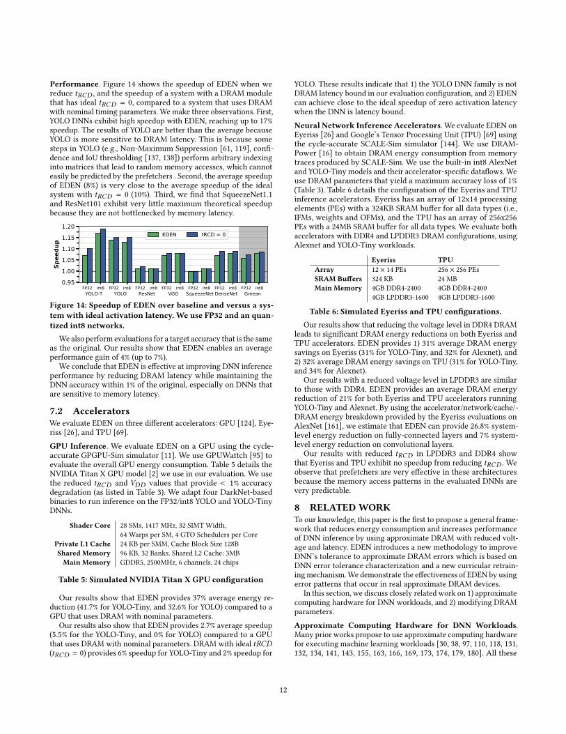
Performance. Figure 14 shows the speedup of EDEN when wereduce tRCD , and the speedup of a system with a DRAM modulethat has ideal tRCD = 0, compared to a system that uses DRAMwith nominal timing parameters. We make three observations. First,YOLO DNNs exhibit high speedup with EDEN, reaching up to 17%speedup. The results of YOLO are better than the average becauseYOLO is more sensitive to DRAM latency. This is because somesteps in YOLO (e.g., Non-Maximum Suppression [61, 119], confi-dence and IoU thresholding [137, 138]) perform arbitrary indexinginto matrices that lead to random memory accesses, which cannoteasily be predicted by the prefetchers . Second, the average speedupof EDEN (8%) is very close to the average speedup of the idealsystem with tRCD = 0 (10%). Third, we find that SqueezeNet1.1and ResNet101 exhibit very little maximum theoretical speedupbecause they are not bottlenecked by memory latency.
FP32 int8 FP32 int8 FP32 int8 FP32 int8 FP32 int8 FP32 int8 FP32 int80.951.001.051.101.151.20
Spee
dup
YOLO-T YOLO ResNet VGG SqueezeNet DenseNet Gmean
EDEN tRCD = 0
Figure 14: Speedup of EDEN over baseline and versus a sys-tem with ideal activation latency. We use FP32 and an quan-tized int8 networks.
We also perform evaluations for a target accuracy that is the sameas the original. Our results show that EDEN enables an averageperformance gain of 4% (up to 7%).
We conclude that EDEN is effective at improving DNN inferenceperformance by reducing DRAM latency while maintaining theDNN accuracy within 1% of the original, especially on DNNs thatare sensitive to memory latency.
7.2 AcceleratorsWe evaluate EDEN on three different accelerators: GPU [124], Eye-riss [26], and TPU [69].
GPU Inference. We evaluate EDEN on a GPU using the cycle-accurate GPGPU-Sim simulator [11]. We use GPUWattch [95] toevaluate the overall GPU energy consumption. Table 5 details theNVIDIA Titan X GPU model [2] we use in our evaluation. We usethe reduced tRCD and VDD values that provide < 1% accuracydegradation (as listed in Table 3). We adapt four DarkNet-basedbinaries to run inference on the FP32/int8 YOLO and YOLO-TinyDNNs.
Shader Core 28 SMs, 1417 MHz, 32 SIMT Width,64 Warps per SM, 4 GTO Schedulers per Core
Private L1 Cache 24 KB per SMM, Cache Block Size 128BShared Memory 96 KB, 32 Banks. Shared L2 Cache: 3MBMain Memory GDDR5, 2500MHz, 6 channels, 24 chips
Table 5: Simulated NVIDIA Titan X GPU configuration
Our results show that EDEN provides 37% average energy re-duction (41.7% for YOLO-Tiny, and 32.6% for YOLO) compared to aGPU that uses DRAM with nominal parameters.
Our results also show that EDEN provides 2.7% average speedup(5.5% for the YOLO-Tiny, and 0% for YOLO) compared to a GPUthat uses DRAM with nominal parameters. DRAM with ideal tRCD(tRCD = 0) provides 6% speedup for YOLO-Tiny and 2% speedup for
YOLO. These results indicate that 1) the YOLO DNN family is notDRAM latency bound in our evaluation configuration, and 2) EDENcan achieve close to the ideal speedup of zero activation latencywhen the DNN is latency bound.
Neural Network Inference Accelerators. We evaluate EDEN onEyeriss [26] and Google’s Tensor Processing Unit (TPU) [69] usingthe cycle-accurate SCALE-Sim simulator [144]. We use DRAM-Power [16] to obtain DRAM energy consumption from memorytraces produced by SCALE-Sim. We use the built-in int8 AlexNetand YOLO-Tiny models and their accelerator-specific dataflows. Weuse DRAM parameters that yield a maximum accuracy loss of 1%(Table 3). Table 6 details the configuration of the Eyeriss and TPUinference accelerators. Eyeriss has an array of 12x14 processingelements (PEs) with a 324KB SRAM buffer for all data types (i.e.,IFMs, weights and OFMs), and the TPU has an array of 256x256PEs with a 24MB SRAM buffer for all data types. We evaluate bothaccelerators with DDR4 and LPDDR3 DRAM configurations, usingAlexnet and YOLO-Tiny workloads.
Eyeriss TPUArray 12 × 14 PEs 256 × 256 PEsSRAM Buffers 324 KB 24 MBMain Memory 4GB DDR4-2400 4GB DDR4-2400
4GB LPDDR3-1600 4GB LPDDR3-1600
Table 6: Simulated Eyeriss and TPU configurations.
Our results show that reducing the voltage level in DDR4 DRAMleads to significant DRAM energy reductions on both Eyeriss andTPU accelerators. EDEN provides 1) 31% average DRAM energysavings on Eyeriss (31% for YOLO-Tiny, and 32% for Alexnet), and2) 32% average DRAM energy savings on TPU (31% for YOLO-Tiny,and 34% for Alexnet).
Our results with a reduced voltage level in LPDDR3 are similarto those with DDR4. EDEN provides an average DRAM energyreduction of 21% for both Eyeriss and TPU accelerators runningYOLO-Tiny and Alexnet. By using the accelerator/network/cache/-DRAM energy breakdown provided by the Eyeriss evaluations onAlexNet [161], we estimate that EDEN can provide 26.8% system-level energy reduction on fully-connected layers and 7% system-level energy reduction on convolutional layers.
Our results with reduced tRCD in LPDDR3 and DDR4 showthat Eyeriss and TPU exhibit no speedup from reducing tRCD . Weobserve that prefetchers are very effective in these architecturesbecause the memory access patterns in the evaluated DNNs arevery predictable.
8 RELATEDWORKTo our knowledge, this paper is the first to propose a general frame-work that reduces energy consumption and increases performanceof DNN inference by using approximate DRAM with reduced volt-age and latency. EDEN introduces a new methodology to improveDNN’s tolerance to approximate DRAM errors which is based onDNN error tolerance characterization and a new curricular retrain-ingmechanism.We demonstrate the effectiveness of EDEN by usingerror patterns that occur in real approximate DRAM devices.
In this section, we discuss closely related work on 1) approximatecomputing hardware for DNN workloads, and 2) modifying DRAMparameters.
Approximate Computing Hardware for DNN Workloads.Many prior works propose to use approximate computing hardwarefor executing machine learning workloads [30, 38, 97, 110, 118, 131,132, 134, 141, 143, 155, 163, 166, 169, 173, 174, 179, 180]. All these
12
works propose techniques for improving DNN tolerance for differ-ent types of approximate hardware mechanisms and error injectionrates. Compared to these works, EDEN is unique in 1) being thefirst work to use approximate DRAM with reduced voltage andlatency, 2) being the first demonstration of DNN inference usingerror characterization of real approximate DRAM devices, 3) usinga novel curricular retraining mechanism that is able to customizethe DNN for tolerating high error rates injected by the target ap-proximate DRAM, and 4) mapping each DNN data type to a DRAMpartition based on the error tolerance of the DNN data type andthe bit error rate of the DRAM partition. We classify related workson approximate hardware for DNN workloads into six categories.
First, works that reduce DRAM refresh to save DNN energy [121,122, 164]. RANA [164] and St-DRC [121] propose to reduce DRAMrefresh rate in the embedded DRAM (eDRAM) memory of DNNaccelerators. Nguyen et al. [122] propose to apply similar refresh op-timization techniques to off-chip DRAM in DNN accelerators. Thesemechanisms use customized retraining mechanisms to improve theaccuracy of the DNN in the presence of a moderate amount oferrors.
Second, works that study the error tolerance of neural networksto uniform random faults in SRAM memory [97, 118, 134, 142, 143].For example, Li et al. [97] analyze the effect of various numericrepresentations on error tolerance. Minerva [135] proposes analgorithm-aware fault mitigation technique to mitigate the effectsof low-voltage SRAM in DNN accelerators.
Third, works that study approximate arithmetic logic in DNNworkloads [141, 141, 178, 179]. ThUnderVolt [178] proposes to un-derscale the voltage of arithmetic elements. Salami et al. [141] andZhang et al. [179] present fault-mitigation techniques for neuralnetworks that minimize errors in faulty registers and logic blockswith pruning and retraining.
Fourth, works that study approximate emerging memory tech-nologies for neural network acceleration. Panda et al. [125] andKim [80] propose neuromorphic accelerators that use spintronicsand memristors to run a proof-of-concept fuzzy neural network.
Fifth, works that study the effects of approximate storage deviceson DNN workloads [132, 155]. Qin et al. [132] study the error toler-ance of neural networks that are stored in approximate non-volatilememory (NVM) media. The authors study the effects of turning theECC off in parts of the NVM media that store the neural networkdata. Wen et al. [155] propose to mitigate the effects of unreliabledisk reads with a specialized ECC variant that aims to mitigateerror patterns present in weights of shallow neural networks.
Sixth, works that study the intrinsic error resilience of DNNs byinjecting randomly-distributed errors in DNN data [110, 110, 141,163, 166, 179, 180]. These works assume that the errors can comefrom any component of the system (i.e., they do not target a specificapproximate hardware component). Marques et al. [110] study theaccuracy of DNNs under different error injection rates and proposevarious error mitigation techniques. This work uses a simple prob-abilistic method to artificially inject errors into the DNN model.ApproxANN [180] uses an algorithm that optimizes the DNN accu-racy by taking into account the error tolerance and the criticality ofeach component of the network. The quality-configurable Neuro-morphic Processing Engine (qcNPE) [166] uses processing elementswith dynamically configurable accuracy for executing approximateneural networks.
Modifying DRAM Parameters. Many prior works study the ef-fects of modifying DRAM parameters on reliability, performanceand energy consumption. We already discuss some prior works
that reduce DRAM voltage, access latency, and refresh rate in Sec-tion 2.3. EDEN leverages the characterization techniques introducedin Voltron [21] and Flexible-Latency DRAM [19] to perform theDRAM characterization required to map a DNN to approximateDRAM with reduced voltage and reduced latency (Section 3.4). Weclassify other related works that modify DRAM parameters intothree categories.
First, works that aim to characterize and reduce energy con-sumption at reduced supply voltage levels [21, 36, 39, 47]. David etal. [36] propose memory dynamic voltage and frequency scaling(DVFS) to reduce DRAM power. MemScale [39] provides dynamicvoltage and/or frequency scaling in main memory to reduce energyconsumption, while meeting a maximum tolerable performancedegradation. Voltron [21] studies voltage reduction in real DRAMdevices in detail and proposes solutions to reduce voltage reliablybased on observed error characteristics and system performancerequirements. VAMPIRE [47] proposes a new DRAM power modelthat is based on the characteristics of real DRAM devices.
Second, works that investigate DRAM characteristics under re-duced access latency [15, 19, 21, 76–78, 93, 94]. Adaptive-LatencyDRAM [94] characterizes the guardbands present in timing parame-ters defined by DRAMmanufacturers, and exploits the extra timingmargins to reliably reduce DRAM latency across different chipsand temperatures. Flexible-Latency DRAM [19] analyzes the spatialdistribution of reduced-latency-induced cell failures, and uses thisinformation to reliably access different regions of DRAM with dif-ferent timing parameters. DIVA-DRAM [93] proposes an automaticmethod for finding the lowest reliable operation latency of DRAM,via a combination of runtime profiling and ECC.
Third, works that aim to reduce DRAM latency by modifying themicroarchitecture of DRAM or the memory controller [31, 56, 57, 91,92, 108, 157, 168]. These works reduce latency without introducingbit errors.
9 CONCLUSIONThis paper introduces EDEN, the first general framework that en-ables energy-efficient and high-performance DNN inference viaapproximate DRAM, while strictly meeting a target DNN accuracy.EDEN uses an iterative mechanism that profiles the DNN and thetarget approximate DRAM with reduced voltage and timing pa-rameters. EDEN improves DNN accuracy with a novel curricularretraining mechanism that tolerates high bit error rates. We evalu-ate EDEN in both simulation and on real hardware. Our evaluationshows that EDEN enables 1) an average DRAM energy reductionof 21%, 37%, 31%, and 32% in CPU, GPU, Eyeriss, and TPU architec-tures, respectively, across a variety of state-of-the-art DNNs, and 2)average (maximum) performance gains of 8% (17%) in CPUs and2.7% (5.5%) in GPUs, for latency-bound DNNs. We expect that thecore principles of EDEN generalize well across different memorydevices, memory parameters, and memory technologies. We hopethat EDEN enables further research and development on the use ofapproximate memory for machine learning workloads.
ACKNOWLEDGMENTSWe thank the anonymous reviewers for feedback. We thank theSAFARI Research Group members for feedback and the stimulat-ing intellectual environment they provide. We acknowledge thegenerous funding provided by our industrial partners: Alibaba, Face-book, Google, Huawei, Intel, Microsoft, and VMware. This researchwas supported in part by the Semiconductor Research Corporation.Skanda Koppula was supported by the Fulbright/Swiss GovernmentExcellent Scholarship 2018.0529.
13

REFERENCES[1] “Intel Xeon CPU E3-1225,” https://ark.intel.com/content/www/us/en/ark/
products/52270/intel-xeon-processor-e3-1225-6m-cache-3-10-ghz.html.[2] “NVIDIA Titan X GPU,” https://www.nvidia.com/en-us/geforce/products/
10series/titan-x-pascal/.[3] “SoftMC Source Code.” https://github.com/CMU-SAFARI/SoftMC[4] “The CIFAR-10 Dataset.” https://www.cs.toronto.edu/~kriz/cifar.html[5] S. Advani, N. Chandramoorthy, K. Swaminathan, K. Irick, Y. C. P. Cho, J. Samp-
son, and V. Narayanan, “Refresh Enabled Video Analytics (REVA): Implicationson Power and Performance of DRAM Supported Embedded Visual Systems,” inICCD, 2014.
[6] J. Albericio, P. Judd, T. Hetherington, T. Aamodt, N. E. Jerger, and A. Moshovos,“Cnvlutin: Ineffectual-Neuron-Free Deep Neural Network Computing,” in ISCA,2016.
[7] M. Alwani, H. Chen,M. Ferdman, and P.Milder, “Fused-Layer CNNAccelerators,”in MICRO, 2016.
[8] R. Andri, L. Cavigelli, D. Rossi, and L. Benini, “YodaNN: An Architecture forUltralow Power Binary-Weight CNN Acceleration,” TCAD, 2017.
[9] A. Aurisano, A. Radovic, D. Rocco, A. Himmel, M. Messier, E. Niner, G. Pawloski,F. Psihas, A. Sousa, and P. Vahle, “A Convolutional Neural Network NeutrinoEvent Classifier,” JINST, 2016.
[10] S. Baek, S. Cho, and R. Melhem, “Refresh Now and Then,” TC, 2013.[11] A. Bakhoda, G. L. Yuan, W. W. Fung, H. Wong, and T. M. Aamodt, “Analyzing
CUDA Workloads using a Detailed GPU Simulator,” in ISPASS, 2009.[12] E. Baseman, N. Debardeleben, S. Blanchard, J. Moore, O. Tkachenko, K. Ferreira,
T. Siddiqua, and V. Sridharan, “Physics-Informed Machine Learning for DRAMError Modeling,” in DFT, 2018.
[13] A. Boroumand, S. Ghose, Y. Kim, R. Ausavarungnirun, E. Shiu, R. Thakur, D. Kim,A. Kuusela, A. Knies, P. Ranganathan, and O. Mutlu, “Google Workloads forConsumer Devices: Mitigating Data Movement Bottlenecks,” in ASPLOS, 2018.
[14] L. Cavigelli and L. Benini, “Origami: A 803-GOp/s/W Convolutional NetworkAccelerator,” TCSVT, 2017.
[15] K. Chandrasekar, S. Goossens, C. Weis, M. Koedam, B. Akesson, N. Wehn, andK. Goossens, “Exploiting Expendable Process-Margins in DRAMs for Run-TimePerformance Optimization,” in DATE, 2014.
[16] K. Chandrasekar, C. Weis, Y. Li, B. Akesson, N. Wehn, and K. Goossens, “DRAM-Power: Open-source DRAM Power & Energy Estimation Tool,” 2012.
[17] K. K. Chang, D. Lee, Z. Chishti, A. R. Alameldeen, C. Wilkerson, Y. Kim, andO. Mutlu, “Improving DRAM Performance by Parallelizing Refreshes with Ac-cesses,” in HPCA, 2014.
[18] K. K. Chang, “Understanding and Improving the Latency of DRAM-Based Mem-ory Systems,” Ph.D. dissertation, Carnegie Mellon Univ., 2017.
[19] K. K. Chang, A. Kashyap, H. Hassan, S. Ghose, K. Hsieh, D. Lee, T. Li, G. Pekhi-menko, S. Khan, and O. Mutlu, “Understanding Latency Variation in ModernDRAM Chips: Experimental Characterization, Analysis, and Optimization,” inSIGMETRICS, 2016.
[20] K. K. Chang, P. J. Nair, D. Lee, S. Ghose, M. K. Qureshi, and O. Mutlu, “Low-CostInter-Linked Subarrays (LISA): Enabling Fast Inter-Subarray Data Movement inDRAM,” in HPCA, 2016.
[21] K. K. Chang, A. G. Yağlıkçı, S. Ghose, A. Agrawal, N. Chatterjee, A. Kashyap,D. Lee, M. O’Connor, H. Hassan, and O. Mutlu, “Understanding Reduced-VoltageOperation in Modern DRAM Devices: Experimental Characterization, Analysis,and Mechanisms,” SIGMETRICS, 2017.
[22] G. Chen, C. Parada, and G. Heigold, “Small-Footprint Keyword Spotting usingDeep Neural Networks.” in ICASSP, 2014.
[23] T. Chen, T. Moreau, Z. Jiang, L. Zheng, S. Jiao, E. Yan, H. Shen, M. Cowan,L. Wang, Y. Hu, L. Ceze, C. Guestrin, and A. Krishnamurthy, “TVM: An Auto-mated End-to-End Optimizing Compiler for Deep Learning,” in OSDI, 2018.
[24] T. Chen, B. Xu, C. Zhang, and C. Guestrin, “Training Deep Nets with SublinearMemory Cost,” arXiv, 2016.
[25] T. Chen, Z. Du, N. Sun, J. Wang, C. Wu, Y. Chen, and O. Temam, “Dian-Nao: A Small-Footprint High-Throughput Accelerator for Ubiquitous Machine-Learning,” ASPLOS, 2014.
[26] Y.-H. Chen, T. Krishna, J. S. Emer, and V. Sze, “Eyeriss: An Energy-EfficientReconfigurable Accelerator for Deep Convolutional Neural Networks,” JSSC,2017.
[27] Y.-H. Chen, T.-J. Yang, J. Emer, and V. Sze, “Eyeriss v2: A Flexible Acceleratorfor Emerging Deep Neural Networks on Mobile Devices,” JETCAS, 2019.
[28] S. Chetlur, C. Woolley, P. Vandermersch, J. Cohen, J. Tran, B. Catanzaro, andE. Shelhamer, “cuDNN: Efficient Primitives for Deep Learning,” arXiv, 2014.
[29] P. Chi, S. Li, C. Xu, T. Zhang, J. Zhao, Y. Liu, Y. Wang, and Y. Xie, “PRIME: ANovel Processing-In-Memory Architecture for Neural Network Computation InReRAM-Based Main Memory,” in ISCA, 2016.
[30] V. K. Chippa, S. T. Chakradhar, K. Roy, and A. Raghunathan, “Analysis and Char-acterization of Inherent Application Resilience for Approximate Computing,” inDAC, 2013.
[31] J. Choi, W. Shin, J. Jang, J. Suh, Y. Kwon, Y. Moon, and L.-S. Kim, “Multiple CloneRow DRAM: A Low Latency and Area Optimized DRAM,” in ISCA, 2015.
[32] Y. Chou, B. Fahs, and S. Abraham, “Microarchitecture Optimizations for Exploit-ing Memory-Level Parallelism,” in ISCA, 2004.
[33] M. Courbariaux, I. Hubara, D. Soudry, R. El-Yaniv, and Y. Bengio, “BinarizedNeural Networks: Training Deep Neural Networks withWeights and ActivationsConstrained to+ 1 or-1,” arXiv, 2016.
[34] Y. L. Cun, J. S. Denker, and S. A. Solla, “Optimal Brain Damage,” in NIPS, 1990.[35] A. Das, H. Hassan, and O. Mutlu, “VRL-DRAM: Improving DRAM Performance
via Variable Refresh Latency,” in DAC, 2018.[36] H. David, C. Fallin, E. Gorbatov, U. R. Hanebutte, and O. Mutlu, “Memory Power
Management via Dynamic Voltage/Frequency Scaling,” in ICAC, 2011.[37] C. De Sa, M. Leszczynski, J. Zhang, A. Marzoev, C. R. Aberger, K. Olukotun, and
C. Ré, “High-Accuracy Low-Precision Training,” arXiv, 2018.[38] J. Deng, Y. Rang, Z. Du, Y. Wang, H. Li, O. Temam, P. Ienne, D. Novo, X. Li,
Y. Chen, and C. Wu, “Retraining-Based Timing Error Mitigation for HardwareNeural Networks,” in DATE, 2015.
[39] Q. Deng, D. Meisner, L. Ramos, T. F. Wenisch, and R. Bianchini, “MemScale:Active Low-Power Modes for Main Memory,” in ASPLOS, 2011.
[40] Q. Deng, L. Jiang, Y. Zhang, M. Zhang, and J. Yang, “DrAcc: A DRAM BasedAccelerator for Accurate CNN Inference,” in DAC, 2018.
[41] C. Dong, C. C. Loy, K. He, and X. Tang, “Learning a Deep Convolutional Networkfor Image Super-Resolution,” in ECCV, 2014.
[42] S. S. Du and J. D. Lee, “On the Power of Over-parametrization in Neural Networkswith Quadratic Activation,” arXiv, 2018.
[43] J. Dundas and T. Mudge, “Improving Data Cache Performance by Pre-executingInstructions Under a Cache Miss,” in ICS, 1997.
[44] J. D. Dundas, “Improving Processor Performance by Dynamically Pre-Processingthe Instruction Stream,” University of Michigan, Tech. Rep., 1999.
[45] M. Gao, J. Pu, X. Yang, M. Horowitz, and C. Kozyrakis, “TETRIS: Scalable andEfficient Neural Network Acceleration with 3D Memory,” ASPLOS, 2017.
[46] S. Ghose, T. Li, N. Hajinazar, D. Senol Cali, and O. Mutlu, “Demystifying ComplexWorkload-DRAM Interactions: An Experimental Study,” in SIGMETRICS, 2019.
[47] S. Ghose, A. G. Yağlıkçı, R. Gupta, D. Lee, K. Kudrolli, W. X. Liu, H. Hassan, K. K.Chang, N. Chatterjee, A. Agrawal, M. O’Connor, and O. Mutlu, “What YourDRAMPowerModels Are Not Telling You: Lessons from aDetailed ExperimentalStudy,” SIGMETRICS, 2018.
[48] A. N. Gomez, M. Ren, R. Urtasun, and R. B. Grosse, “The Reversible ResidualNetwork: Backpropagation without Storing Activations,” in NIPS, 2017.
[49] A. Graves and N. Jaitly, “Towards End-to-End Speech Recognition with Recur-rent Neural Networks,” in ICML, 2014.
[50] S. Gu, E. Holly, T. Lillicrap, and S. Levine, “Deep Reinforcement Learning forRobotic Manipulation with Asynchronous Off-Policy Updates,” in ICRA, 2017.
[51] M. Guan and L. Wang, “Temperature Aware Refresh for DRAM PerformanceImprovement in 3D ICs,” in ISQED, 2015.
[52] K. Guo, L. Sui, J. Qiu, J. Yu, J. Wang, S. Yao, S. Han, Y. Wang, and H. Yang,“Angel-Eye: A Complete Design Flow for Mapping CNN onto Embedded FPGA,”TCAD, 2017.
[53] T. Hamamoto, S. Sugiura, and S. Sawada, “On the Retention Time Distributionof Dynamic Random Access Memory (DRAM),” TED, 1998.
[54] S. Han, X. Liu, H. Mao, J. Pu, A. Pedram, M. A. Horowitz, and W. J. Dally, “EIE:Efficient Inference Engine on Compressed Deep Neural Network,” in ISCA, 2016.
[55] S. Han, H. Mao, and W. J. Dally, “Deep Compression: Compressing Deep NeuralNetworks with Pruning, Trained Quantization and Huffman Coding,” arXiv,2015.
[56] H. Hassan, G. Pekhimenko, N. Vijaykumar, V. Seshadri, D. Lee, O. Ergin, andO. Mutlu, “ChargeCache: Reducing DRAM Latency by Exploiting Row AccessLocality,” in HPCA, 2016.
[57] H. Hassan, M. Patel, J. S. Kim, A. G. Yaglikci, N. Vijaykumar, N. Mansouri Ghiasi,S. Ghose, and O. Mutlu, “CROW : A Low-Cost Substrate for Improving DRAMPerformance, Energy Efficiency, and Reliability,” in ISCA, 2019.
[58] H. Hassan, N. Vijaykumar, S. Khan, S. Ghose, K. Chang, G. Pekhimenko, D. Lee,O. Ergin, and O. Mutlu, “SoftMC: A Flexible and Practical Open-Source Infras-tructure for Enabling Experimental DRAM Studies,” in HPCA, 2017.
[59] K. He, X. Zhang, S. Ren, and J. Sun, “Deep Residual Learning for Image Recogni-tion,” in CVPR, 2016.
[60] Y. He, J. Lin, Z. Liu, H. Wang, L.-J. Li, and S. Han, “AMC: AutoML for ModelCompression and Acceleration on Mobile Devices,” in ECCV, 2018.
[61] J. Hosang, R. Benenson, and B. Schiele, “Learning Non-maximum Suppression,”in CVPR, 2017.
[62] I. Hubara, M. Courbariaux, D. Soudry, R. El-Yaniv, and Y. Bengio, “QuantizedNeural Networks: Training Neural Networks with Low Precision Weights andActivations,” IMLR, 2017.
[63] F. Iandola, M. Moskewicz, S. Karayev, R. Girshick, T. Darrell, and K. Keutzer,“DenseNet: Implementing Efficient ConvNet Descriptor Pyramids,” arXiv, 2014.
[64] F. N. Iandola, S. Han, M. W. Moskewicz, K. Ashraf, W. J. Dally, and K. Keutzer,“SqueezeNet: AlexNet-Level Accuracy with 50x Fewer Parameters and< 0.5 mbModel Size,” arXiv, 2016.
[65] M. Imani, M. Samragh, Y. Kim, S. Gupta, F. Koushanfar, and T. Rosing, “RAPIDNN:In-Memory Deep Neural Network Acceleration Framework,” arXiv, 2018.
[66] B. Jacob, S. Kligys, B. Chen, M. Zhu, M. Tang, A. Howard, H. Adam, andD. Kalenichenko, “Quantization and Training of Neural Networks for EfficientInteger-Arithmetic-Only Inference,” in CVPR, 2018.
[67] JEDEC Standard, “DDR4 SDRAM Specification (JESD79-4),” 2012.[68] W. Jin, C. Coley, R. Barzilay, and T. Jaakkola, “Predicting Organic Reaction
Outcomes with Weisfeiler-Lehman Network,” in NIPS, 2017.[69] N. P. Jouppi, C. Young, N. Patil, D. Patterson, G. Agrawal, R. Bajwa, S. Bates,
S. Bhatia, N. Boden, A. Borchers et al., “In-Datacenter Performance Analysis ofa Tensor Processing Unit,” in ISCA, 2017.
14
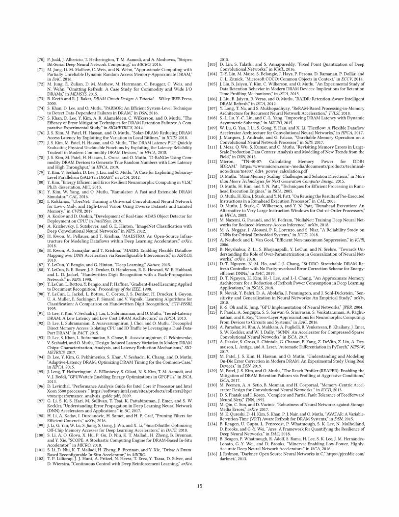
[70] P. Judd, J. Albericio, T. Hetherington, T. M. Aamodt, and A. Moshovos, “Stripes:Bit-Serial Deep Neural Network Computing,” in MICRO, 2016.
[71] M. Jung, D. M. Mathew, C. Weis, and N. Wehn, “Approximate Computing withPartially Unreliable Dynamic Random Access Memory-Approximate DRAM,”in DAC, 2016.
[72] M. Jung, É. Zulian, D. M. Mathew, M. Herrmann, C. Brugger, C. Weis, andN. Wehn, “Omitting Refresh: A Case Study for Commodity and Wide I/ODRAMs,” in MEMSYS, 2015.
[73] B. Keeth and R. J. Baker, DRAM Circuit Design: A Tutorial. Wiley-IEEE Press,2000.
[74] S. Khan, D. Lee, and O. Mutlu, “PARBOR: An Efficient System-Level Techniqueto Detect Data-Dependent Failures in DRAM,” in DSN, 2016.
[75] S. Khan, D. Lee, Y. Kim, A. R. Alameldeen, C. Wilkerson, and O. Mutlu, “TheEfficacy of Error Mitigation Techniques for DRAM Retention Failures: A Com-parative Experimental Study,” in SIGMETRICS, 2014.
[76] J. S. Kim, M. Patel, H. Hassan, and O. Mutlu, “Solar-DRAM: Reducing DRAMAccess Latency by Exploiting the Variation in Local Bitlines,” in ICCD, 2018.
[77] J. S. Kim, M. Patel, H. Hassan, and O. Mutlu, “The DRAM Latency PUF: QuicklyEvaluating Physical Unclonable Functions by Exploiting the Latency-ReliabilityTradeoff in Modern Commodity DRAM Devices,” in HPCA, 2018.
[78] J. S. Kim, M. Patel, H. Hassan, L. Orosa, and O. Mutlu, “D-RaNGe: Using Com-modity DRAM Devices to Generate True Random Numbers with Low Latencyand High Throughput,” in HPCA, 2019.
[79] Y. Kim, V. Seshadri, D. Lee, J. Liu, and O. Mutlu, “A Case for Exploiting Subarray-Level Parallelism (SALP) in DRAM,” in ISCA, 2012.
[80] Y. Kim, “Energy Efficient and Error Resilient Neuromorphic Computing in VLSI,”Ph.D. dissertation, MIT, 2013.
[81] Y. Kim, W. Yang, and O. Mutlu, “Ramulator: A Fast and Extensible DRAMSimulator.” CAL, 2016.
[82] I. Kokkinos, “UberNet: Training a Universal Convolutional Neural Networkfor Low-, Mid-, and High-Level Vision Using Diverse Datasets and LimitedMemory.” in CVPR, 2017.
[83] A. Kozlov and D. Osokin, “Development of Real-time ADAS Object Detector forDeployment on CPU,” in IntelliSys, 2019.
[84] A. Krizhevsky, I. Sutskever, and G. E. Hinton, “ImageNet Classification withDeep Convolutional Neural Networks,” in NIPS, 2012.
[85] H. Kwon, M. Pellauer, and T. Krishna, “MAESTRO: An Open-Source Infras-tructure for Modeling Dataflows within Deep Learning Accelerators,” arXiv,2018.
[86] H. Kwon, A. Samajdar, and T. Krishna, “MAERI: Enabling Flexible DataflowMapping over DNN Accelerators via Reconfigurable Interconnects,” in ASPLOS,2018.
[87] Y. LeCun, Y. Bengio, and G. Hinton, “Deep Learning,” Nature, 2015.[88] Y. LeCun, B. E. Boser, J. S. Denker, D. Henderson, R. E. Howard, W. E. Hubbard,
and L. D. Jackel, “Handwritten Digit Recognition with a Back-PropagationNetwork,” in NIPS, 1990.
[89] Y. LeCun, L. Bottou, Y. Bengio, and P. Haffner, “Gradient-Based Learning Appliedto Document Recognition,” Proceedings of the IEEE, 1998.
[90] Y. LeCun, L. Jackel, L. Bottou, C. Cortes, J. S. Denker, H. Drucker, I. Guyon,U. A. Muller, E. Sackinger, P. Simard, and V. Vapnik, “Learning Algorithms forClassification: A Comparison on Handwritten Digit Recognition,” CTP-PBSRI,1995.
[91] D. Lee, Y. Kim, V. Seshadri, J. Liu, L. Subramanian, and O. Mutlu, “Tiered-LatencyDRAM: A Low Latency and Low Cost DRAM Architecture,” in HPCA, 2013.
[92] D. Lee, L. Subramanian, R. Ausavarungnirun, J. Choi, and O. Mutlu, “DecoupledDirect Memory Access: Isolating CPU and IO Traffic by Leveraging a Dual-Data-Port DRAM,” in PACT, 2015.
[93] D. Lee, S. Khan, L. Subramanian, S. Ghose, R. Ausavarungnirun, G. Pekhimenko,V. Seshadri, and O. Mutlu, “Design-Induced Latency Variation in Modern DRAMChips: Characterization, Analysis, and Latency Reduction Mechanisms,” SIG-METRICS, 2017.
[94] D. Lee, Y. Kim, G. Pekhimenko, S. Khan, V. Seshadri, K. Chang, and O. Mutlu,“Adaptive-Latency DRAM: Optimizing DRAM Timing for the Common-Case,”in HPCA, 2015.
[95] J. Leng, T. Hetherington, A. ElTantawy, S. Gilani, N. S. Kim, T. M. Aamodt, andV. J. Reddi, “GPUWattch: Enabling Energy Optimizations in GPGPUs,” in ISCA,2013.
[96] D. Levinthal, “Performance Analysis Guide for Intel Core i7 Processor and IntelXeon 5500 processors ,” https://software.intel.com/sites/products/collateral/hpc/vtune/performance_analysis_guide.pdf, 2009.
[97] G. Li, S. K. S. Hari, M. Sullivan, T. Tsai, K. Pattabiraman, J. Emer, and S. W.Keckler, “Understanding Error Propagation in Deep Learning Neural Network(DNN) Accelerators and Applications,” in SC, 2017.
[98] H. Li, A. Kadav, I. Durdanovic, H. Samet, and H. P. Graf, “Pruning Filters forEfficient Convnets,” arXiv, 2016.
[99] J. Li, G. Yan, W. Lu, S. Jiang, S. Gong, J. Wu, and X. Li, “SmartShuttle: OptimizingOff-Chip Memory Accesses for Deep Learning Accelerators,” in DATE, 2018.
[100] S. Li, A. O. Glova, X. Hu, P. Gu, D. Niu, K. T. Malladi, H. Zheng, B. Brennan,and Y. Xie, “SCOPE: A Stochastic Computing Engine for DRAM-Based In-SituAccelerator.” in MICRO, 2018.
[101] S. Li, D. Niu, K. T. Malladi, H. Zheng, B. Brennan, and Y. Xie, “Drisa: A Dram-Based Reconfigurable In-Situ Accelerator,” in MICRO.
[102] T. P. Lillicrap, J. J. Hunt, A. Pritzel, N. Heess, T. Erez, Y. Tassa, D. Silver, andD. Wierstra, “Continuous Control with Deep Reinforcement Learning,” arXiv,
2015.[103] D. Lin, S. Talathi, and S. Annapureddy, “Fixed Point Quantization of Deep
Convolutional Networks,” in ICML, 2016.[104] T.-Y. Lin, M. Maire, S. Belongie, J. Hays, P. Perona, D. Ramanan, P. Dollár, and
C. L. Zitnick, “Microsoft COCO: Common Objects in Context,” in ECCV, 2014.[105] J. Liu, B. Jaiyen, Y. Kim, C. Wilkerson, and O. Mutlu, “An Experimental Study of
Data Retention Behavior in Modern DRAM Devices: Implications for RetentionTime Profiling Mechanisms,” in ISCA, 2013.
[106] J. Liu, B. Jaiyen, R. Veras, and O. Mutlu, “RAIDR: Retention-Aware IntelligentDRAM Refresh,” in ISCA, 2012.
[107] Y. Long, T. Na, and S. Mukhopadhyay, “ReRAM-Based Processing-in-MemoryArchitecture for Recurrent Neural Network Acceleration,” TVLSI, 2018.
[108] S.-L. Lu, Y.-C. Lin, and C.-L. Yang, “Improving DRAM Latency with DynamicAsymmetric Subarray,” in MICRO, 2015.
[109] W. Lu, G. Yan, J. Li, S. Gong, Y. Han, and X. Li, “Flexflow: A Flexible DataflowAccelerator Architecture for Convolutional Neural Networks,” in HPCA, 2017.
[110] J. Marques, J. Andrade, and G. Falcao, “Unreliable Memory Operation on aConvolutional Neural Network Processor,” in SiPS, 2017.
[111] J. Meza, Q. Wu, S. Kumar, and O. Mutlu, “Revisiting Memory Errors in Large-Scale Production Data Centers: Analysis and Modeling of New Trends from theField,” in DSN, 2015.
[112] Micron, “TN-40-07: Calculating Memory Power for DDR4SDRAM.” https://www.micron.com/-/media/documents/products/technical-note/dram/tn4007_ddr4_power_calculation.pdf
[113] O. Mutlu, “Main Memory Scaling: Challenges and Solution Directions,” in Morethan Moore Technologies for Next Generation Computer Design, 2015.
[114] O. Mutlu, H. Kim, and Y. N. Patt, “Techniques for Efficient Processing in Runa-head Execution Engines,” in ISCA, 2005.
[115] O.Mutlu, H. Kim, J. Stark, and Y. N. Patt, “On Reusing the Results of Pre-ExecutedInstructions in a Runahead Execution Processor,” in CAL, 2005.
[116] O. Mutlu, J. Stark, C. Wilkerson, and Y. N. Patt, “Runahead Execution: AnAlternative to Very Large Instruction Windows for Out-of-Order Processors,”in HPCA, 2003.
[117] M. Nazemi, G. Pasandi, and M. Pedram, “NullaNet: Training Deep Neural Net-works for Reduced-Memory-Access Inference,” arXiv, 2018.
[118] M. A. Neggaz, I. Alouani, P. R. Lorenzo, and S. Niar, “A Reliability Study onCNNs for Critical Embedded Systems,” in ICCD, 2018.
[119] A. Neubeck and L. Van Gool, “Efficient Non-maximum Suppression,” in ICPR,2006.
[120] B. Neyshabur, Z. Li, S. Bhojanapalli, Y. LeCun, and N. Srebro, “Towards Un-derstanding the Role of Over-Parametrization in Generalization of Neural Net-works,” arXiv, 2018.
[121] D.-T. Nguyen, N.-M. Ho, and I.-J. Chang, “St-DRC: Stretchable DRAM Re-fresh Controller with No Parity-overhead Error Correction Scheme for Energy-efficient DNNs,” in DAC, 2019.
[122] D. T. Nguyen, H. Kim, H.-J. Lee, and I.-J. Chang, “An Approximate MemoryArchitecture for a Reduction of Refresh Power Consumption in Deep LearningApplications,” in ISCAS, 2018.
[123] R. Novak, Y. Bahri, D. A. Abolafia, J. Pennington, and J. Sohl-Dickstein, “Sen-sitivity and Generalization in Neural Networks: An Empirical Study,” arXiv,2018.
[124] K.-S. Oh and K. Jung, “GPU Implementation of Neural Networks,” JPRR, 2004.[125] P. Panda, A. Sengupta, S. S. Sarwar, G. Srinivasan, S. Venkataramani, A. Raghu-
nathan, and K. Roy, “Cross-Layer Approximations for Neuromorphic Computing:From Devices to Circuits and Systems,” in DAC, 2016.
[126] A. Parashar, M. Rhu, A. Mukkara, A. Puglielli, R. Venkatesan, B. Khailany, J. Emer,S. W. Keckler, and W. J. Dally, “SCNN: An Accelerator for Compressed-SparseConvolutional Neural Networks,” in ISCA, 2017.
[127] A. Paszke, S. Gross, S. Chintala, G. Chanan, E. Yang, Z. DeVito, Z. Lin, A. Des-maison, L. Antiga, and A. Lerer, “Automatic Differentiation in PyTorch,” NIPS-W,2017.
[128] M. Patel, J. S. Kim, H. Hassan, and O. Mutlu, “Understanding and ModelingOn-Die Error Correction in Modern DRAM: An Experimental Study Using RealDevices,” in DSN, 2019.
[129] M. Patel, J. S. Kim, and O. Mutlu, “The Reach Profiler (REAPER): Enabling theMitigation of DRAM Retention Failures via Profiling at Aggressive Conditions,”ISCA, 2017.
[130] M. Peemen, A. A. Setio, B. Mesman, and H. Corporaal, “Memory-Centric Accel-erator Design for Convolutional Neural Networks.” in ICCD, 2013.
[131] D. S. Phatak and I. Koren, “Complete and Partial Fault Tolerance of FeedforwardNeural Nets,” TNN, 1995.
[132] M. Qin, C. Sun, and D. Vucinic, “Robustness of Neural Networks against StorageMedia Errors,” arXiv, 2017.
[133] M. K. Qureshi, D.-H. Kim, S. Khan, P. J. Nair, and O. Mutlu, “AVATAR: A Variable-Retention-Time (VRT) Aware Refresh for DRAM Systems,” in DSN, 2015.
[134] B. Reagen, U. Gupta, L. Pentecost, P. Whatmough, S. K. Lee, N. Mulholland,D. Brooks, and G.-Y. Wei, “Ares: A Framework for Quantifying the Resilience ofDeep Neural Networks,” in DAC, 2018.
[135] B. Reagen, P. Whatmough, R. Adolf, S. Rama, H. Lee, S. K. Lee, J. M. Hernández-Lobato, G.-Y. Wei, and D. Brooks, “Minerva: Enabling Low-Power, Highly-Accurate Deep Neural Network Accelerators,” in ISCA, 2016.
[136] J. Redmon, “Darknet: Open Source Neural Networks in C,” https://pjreddie.com/darknet/, 2013.
15

[137] J. Redmon and A. Farhadi, “YOLO9000: Better, Faster, Stronger,” arXiv, 2017.[138] H. Rezatofighi, N. Tsoi, J. Gwak, A. Sadeghian, I. Reid, and S. Savarese, “General-
ized Intersection Over Union: AMetric and a Loss for Bounding Box Regression,”in CVPR, 2019.
[139] H. Robbins and S. Monro, “A Stochastic Approximation Method,” The Annals ofMathematical Statistics, 1951.
[140] O. Russakovsky, J. Deng, H. Su, J. Krause, S. Satheesh, S. Ma, Z. Huang, A. Karpa-thy, A. Khosla, M. Bernstein, A. C. Berg, and L. Fei-Fei, “ImageNet Large ScaleVisual Recognition Challenge,” IJCV, 2015.
[141] B. Salami, O. Unsal, and A. Cristal, “On the Resilience of RTL NN Accelerators:Fault Characterization and Mitigation,” arXiv, 2018.
[142] B. Salami, O. S. Unsal, and A. C. Kestelman, “Comprehensive Evaluation ofSupply Voltage Underscaling in FPGA On-chip Memories,” in MICRO, 2018.
[143] A. H. Salavati and A. Karbasi, “Multi-Level Error-Resilient Neural Networks,” inISIT, 2012.
[144] A. Samajdar, Y. Zhu, P. N. Whatmough, M. Mattina, and T. Krishna, “SCALE-Sim:Systolic CNN Accelerator,” in arXiv, 2018.
[145] D. Sanchez and C. Kozyrakis, “ZSim: Fast and Accurate MicroarchitecturalSimulation of Thousand-Core Systems,” in ISCA, 2013.
[146] M. Sandler, A. Howard, M. Zhu, A. Zhmoginov, and L.-C. Chen, “MobileNetV2:The Next Generation of On-Device Computer Vision Networks,” in CVPR, 2018.
[147] B. Schroeder, E. Pinheiro, and W.-D. Weber, “DRAM Errors in the Wild: ALarge-Scale Field Study,” in SIGMETRICS, 2009.
[148] F. Schuiki, M. Schaffner, F. K. Gürkaynak, and L. Benini, “A Scalable Near-Memory Architecture for Training Deep Neural Networks on Large In-MemoryDatasets,” arXiv, 2018.
[149] M. H. Segler, T. Kogej, C. Tyrchan, and M. P. Waller, “Generating FocusedMolecule Libraries for Drug Discovery with Recurrent Neural Networks,” ACScentral science, 2017.
[150] V. Seshadri, D. Lee, T. Mullins, H. Hassan, A. Boroumand, J. Kim, M. A. Kozuch,O. Mutlu, P. B. Gibbons, and T. C. Mowry, “Ambit: In-Memory Accelerator forBulk Bitwise Operations Using Commodity DRAM Technology,” in MICRO,2017.
[151] V. Seshadri and O. Mutlu, “In-DRAM Bulk Bitwise Execution Engine,” arXiv,2019.
[152] A. Shafiee, A. Nag, N. Muralimanohar, R. Balasubramonian, J. P. Strachan, M. Hu,R. S. Williams, and V. Srikumar, “ISAAC: A Convolutional Neural NetworkAccelerator with In-Situ Analog Arithmetic In Crossbars,” ISCA, 2016.
[153] N. Shazeer, A. Mirhoseini, K. Maziarz, A. Davis, Q. Le, G. Hinton, and J. Dean,“Outrageously Large Neural Networks: The Sparsely-Gated Mixture-of-ExpertsLayer,” arXiv, 2017.
[154] Y. Shen, M. Ferdman, and P. Milder, “Escher: A CNN Accelerator with FlexibleBuffering to Minimize Off-Chip Transfer,” in FCCM, 2017.
[155] W. Shi, Y. Wen, Z. Liu, X. Zhao, D. Boumber, R. Vilalta, and L. Xu, “Fault ResilientPhysical Neural Networks on a Single Chip,” in CASES, 2014.
[156] K. Simonyan and A. Zisserman, “Very Deep Convolutional Networks for Large-Scale Image Recognition,” arXiv, 2014.
[157] Y. H. Son, O. Seongil, Y. Ro, J. W. Lee, and J. H. Ahn, “Reducing Memory AccessLatency with Asymmetric DRAM Bank Organizations,” in ISCA, 2013.
[158] L. Song, Y. Wang, Y. Han, X. Zhao, B. Liu, and X. Li, “C-Brain: A Deep LearningAccelerator that Tames the Diversity of CNNs through Adaptive Data-LevelParallelization,” in DAC, 2016.
[159] E. Sprangle and D. Carmean, “Increasing Processor Performance by Implement-ing Deeper Pipelines,” in ISCA, 2002.
[160] N. Srivastava, G. Hinton, A. Krizhevsky, I. Sutskever, and R. Salakhutdinov,“Dropout: A Simple Way to Prevent Neural Networks from Overfitting,” JMLR,2014.
[161] V. Sze, Y.-H. Chen, T.-J. Yang, and J. S. Emer, “Efficient Processing of Deep NeuralNetworks: A tutorial and Survey,” Proceedings of the IEEE, 2017.
[162] X. Tang, M. Kandemir, P. Yedlapalli, and J. Kotra, “Improving Bank-Level Paral-lelism for Irregular Applications,” in MICRO, 2016.
[163] O. Temam, “A Defect-Tolerant Accelerator for Emerging High-PerformanceApplications,” in ISCA, 2012.
[164] F. Tu, W. Wu, S. Yin, L. Liu, and S. Wei, “RANA: Towards Efficient NeuralAcceleration with Refresh-Optimized Embedded DRAM,” in ISCA, 2018.
[165] K. Ueyoshi, K. Ando, K. Hirose, S. Takamaeda-Yamazaki, J. Kadomoto, T. Miy-ata, M. Hamada, T. Kuroda, and M. Motomura, “QUEST: A 7.49 TOPS Multi-Purpose Log-Quantized DNN Inference Engine Stacked on 96MB 3D SRAMUsing Inductive-Coupling Technology in 40nm CMOS,” in ISSCC, 2018.
[166] S. Venkataramani, A. Ranjan, K. Roy, and A. Raghunathan, “AxNN: Energy-Efficient Neuromorphic Systems using Approximate Computing,” in ISLPED,2014.
[167] T. Vogelsang, “Understanding the Energy Consumption of Dynamic RandomAccess Memories,” in MICRO, 2010.
[168] Y. Wang, A. Tavakkol, L. Orosa, S. Ghose, N. M. Ghiasi, M. Patel, J. S. Kim,H. Hassan, M. Sadrosadati, and O. Mutlu, “Reducing DRAM Latency via Charge-Level-Aware Look-Ahead Partial Restoration,” in MICRO, 2018.
[169] P. N. Whatmough, S. K. Lee, H. Lee, S. Rama, D. Brooks, and G. Wei, “14.3 A28nm SoC with a 1.2GHz 568nJ/Prediction Sparse Deep-Neural-Network Enginewith >0.1 Timing Error Rate Tolerance for IoT Applications,” in ISSCC, 2017.
[170] J. Wu, C. Leng, Y. Wang, Q. Hu, and J. Cheng, “Quantized Convolutional NeuralNetworks for Mobile Devices,” in CVPR, 2016.
[171] S. Xie, R. Girshick, P. Dollár, Z. Tu, and K. He, “Aggregated Residual Transfor-mations for Deep Neural Networks,” in CVPR, 2017.
[172] H. Yang, Y. Zhu, and J. Liu, “ECC: Platform-Independent Energy-ConstrainedDeep Neural Network Compression via a Bilinear Regression Model,” in CVPR,2019.
[173] L. Yang and B. Murmann, “Approximate SRAM for Energy-Efficient, Privacy-Preserving Convolutional Neural Networks,” in ISVLSI, 2017.
[174] L. Yang and B. Murmann, “SRAM Voltage Scaling for Energy-Efficient Convolu-tional Neural Networks,” in ISQED, 2017.
[175] T.-J. Yang, Y.-H. Chen, and V. Sze, “Designing Energy-Efficient ConvolutionalNeural Networks using Energy-Aware Pruning,” in CVPR, 2017.
[176] T.-J. Yang, A. Howard, B. Chen, X. Zhang, A. Go, M. Sandler, V. Sze, and H. Adam,“NetAdapt: Platform-AwareNeural NetworkAdaptation forMobile Applications,”in ECCV, 2018.
[177] J. Yu, A. Lukefahr, D. Palframan, G. Dasika, R. Das, and S. Mahlke, “Scalpel:Customizing DNN Pruning to the Underlying Hardware Parallelism,” in ISCA,2017.
[178] J. Zhang, K. Rangineni, Z. Ghodsi, and S. Garg, “Thundervolt: Enabling Ag-gressive Voltage Underscaling and Timing Error Resilience for Energy EfficientDeep Learning Accelerators,” in DAC, 2018.
[179] J. J. Zhang, T. Gu, K. Basu, and S. Garg, “Analyzing and Mitigating the Impactof Permanent Faults on a Systolic Array Based Neural Network Accelerator,” inVTS, 2018.
[180] Q. Zhang, T. Wang, Y. Tian, F. Yuan, and Q. Xu, “ApproxANN: An ApproximateComputing Framework for Artificial Neural Network,” in DATE, 2015.
[181] S. Zhang, Z. Du, L. Zhang, H. Lan, S. Liu, L. Li, Q. Guo, T. Chen, and Y. Chen,“Cambricon-X: An Accelerator for Sparse Neural Networks,” in MICRO, 2016.
[182] T. Zhang, K. Chen, C. Xu, G. Sun, T. Wang, and Y. Xie, “Half-DRAM: A High-Bandwidth and Low-power DRAM Architecture from the Rethinking of Fine-grained Activation,” in ISCA, 2014.
[183] X. Zhang, Y. Zhang, B. Childers, and J. Yang, “AWARD: Approximation-aWAreRestore in Further Scaling DRAM,” in MEMSYS, 2016.
[184] C. Zhu, S. Han, H. Mao, and W. J. Dally, “Trained Ternary Quantization,” arXiv,2016.
16