ecen720: high-speed links circuits and systems...
TRANSCRIPT

Sam PalermoAnalog & Mixed-Signal Center
Texas A&M University
ECEN720: High-Speed Links Circuits and Systems
Spring 2014
Lecture 15: Optical I/O

Announcements
• Exam 2 is on Thursday April 24• Comprehensive, but will focus on lectures 7-14• 85 minutes• 1 standard 8.5x11 note sheet (front & back)• Bring your calculator
2

Agenda
• Electrical Channel Issues• Optical Channel• Optical Transmitter Technology• Optical Receiver Technology• Optical Integration Approaches
3

High-Speed Electrical Link System
4
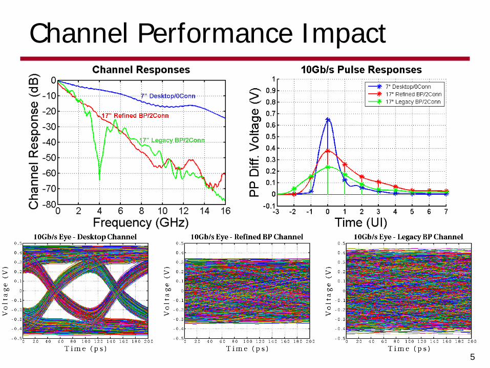
Channel Performance Impact
5

Link with EqualizationSe
rializ
er
DTX[N:0]
TX Clk Generation
(PLL)
TX FIR Equalization
RX Clk Recovery
(CDR/Fwd Clk)
Σ
RX CTLE + DFE Equalization
Des
eria
lizer
DRX[N:0]
Channel
f
6

Channel Performance Impact
7

High-Speed Optical Link System
Optical Channel• Optical interconnects remove many channel limitations• Reduced complexity and power
consumption• Potential for high information density with
wavelength-division multiplexing (WDM)
8
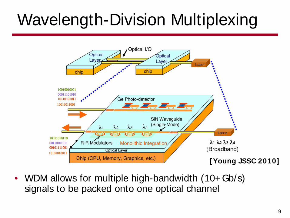
Wavelength-Division Multiplexing
• WDM allows for multiple high-bandwidth (10+Gb/s) signals to be packed onto one optical channel
[Young JSSC 2010]
9

Agenda
• Electrical Channel Issues• Optical Channel• Optical Transmitter Technology• Optical Receiver Technology• Optical Integration Approaches
10

Optical Channels
• Short distance optical I/O channels are typically either waveguide (fiber)-based or free-space
• Optical channel advantages• Much lower loss• Lower cross-talk• Smaller waveguides relative to electrical traces• Potential for multiple data channels on single
fiber via WDM
11

Waveguide (Fiber)-Based Optical Links
• Optical fiber loss is specified in dB/km• Single-Mode Fiber loss
~0.25dB/km at 1550nm• RF coaxial cable loss ~100dB/km
at 10GHz
• Frequency dependent loss is very small• <0.5dB/km over a bandwidth
>10THz
• Bandwidth may be limited by dispersion (pulse-spreading)• Important to limit laser linewidth
for long distances (>1km)
n2
n1core
cladding For TIR: n1 > n2
Optical Fiber Cross-Section
Single-Mode Fiber Loss & Dispersion
[Sackinger]12

Inter-Chip Waveguide Examples
• Typical differential electrical strip lines are at ~500µm pitch
12-Channel Ribbon Fiber
Optical Polymer Waveguide in PCB
[Reflex Photonics][Immonen 2009]
12 channels at a 250µm pitch10Gb/s mod. → 40Gb/s/mm
<100µm channel pitch possible10Gb/s mod. → 100+Gb/s/mm
13

Free-Space Optical Links
• Free-space (air or glass) interconnect systems have also been proposed
• Optical imaging system routes light chip-to-chip
[Gruber]
14
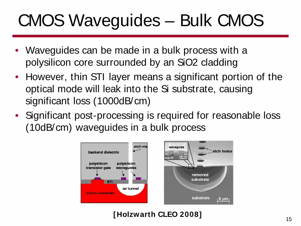
CMOS Waveguides – Bulk CMOS
• Waveguides can be made in a bulk process with a polysilicon core surrounded by an SiO2 cladding
• However, thin STI layer means a significant portion of the optical mode will leak into the Si substrate, causing significant loss (1000dB/cm)
• Significant post-processing is required for reasonable loss (10dB/cm) waveguides in a bulk process
[Holzwarth CLEO 2008]15
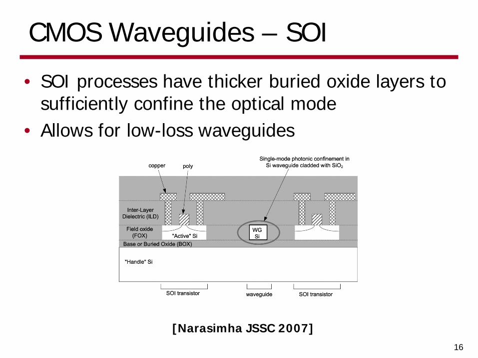
CMOS Waveguides – SOI
• SOI processes have thicker buried oxide layers to sufficiently confine the optical mode
• Allows for low-loss waveguides
[Narasimha JSSC 2007]16

CMOS Waveguides – Back-End Processing
• Waveguides & optical devices can be fabricated above metallization
• Reduces active area consumption
• Allows for independent optimization of transistor and optical device processes
[Young JSSC 2010]
17

Agenda
• Electrical Channel Issues• Optical Channel• Optical Transmitter Technology• Optical Receiver Technology• Optical Integration Approaches
18

Optical Modulation Techniques
• Due to it’s narrow frequency (wavelength) spectrum, a single-longitudinal mode (SLM) laser source often generates the optical power that is modulated for data communication• This is required for long-haul (multi-km) communication• May not be necessary for short distance (~100m) chip-to-chip I/Os
• Two modulation techniques• Direct modulation of laser• External modulation of continuous-wave (CW) “DC” laser with
absorptive or refractive modulators
19

• Directly modulating laser output power• Simplest approach• Introduces laser “chirp”, which is unwanted frequency
(wavelength) modulation• This chirp causes unwanted pulse dispersion when passed
through a long fiber
Directly Modulated Laser
20

• External modulation of continuous-wave (CW) “DC” laser with absorptive or refractive modulators• Adds an extra component• Doesn’t add chirp, and allows for a transform limited
spectrum
Externally Modulated Laser
21

Optical Sources for Chip-to-Chip Links
• Vertical-Cavity Surface-Emitting Laser (VCSEL)
• Mach-Zehnder Modulator (MZM)
• Electro-Absorption Modulator (EAM)
• Ring-Resonator Modulator (RRM)
22

Vertical-Cavity Surface-Emitting Laser (VCSEL)
• VCSEL emits light perpendicular from top (or bottom) surface
• Important to always operate VCSEL above threshold current, ITH, to prevent “turn-on delay” which results in ISI
• Operate at finite extinction ratio (P1/P0)
n-contact
p-contact
gain regionoxide layer
bottom mirror
top mirror
light output
ITH = 700µAη = 0.37mW/mA
( )
∆∆
=
−=
AW Efficiency Slope
IP
IIP THo
η
η
VCSEL Cross-Section VCSEL L-I-V Curves
η
23
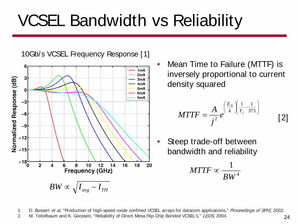
VCSEL Bandwidth vs Reliability
THavg IIBW −∝
−
= 37311
2j
ATk
E
ejAMTTF
10Gb/s VCSEL Frequency Response [1]
4
1BW
MTTF ∝
• Mean Time to Failure (MTTF) is inversely proportional to current density squared
[2]
• Steep trade-off between bandwidth and reliability
1. D. Bossert et al, "Production of high-speed oxide confined VCSEL arrays for datacom applications," Proceedings of SPIE, 2002.2. M. Teitelbaum and K. Goossen, "Reliability of Direct Mesa Flip-Chip Bonded VCSEL’s," LEOS, 2004. 24

VCSEL Drivers
• Current-mode drivers often used due to linear L-I relationship
• Equalization can be added to extend VCSEL bandwidth for a given current density
D+
D-
Dummy Load
LVddPout
Imod Ibias
S. Palermo and M. Horowitz, “High-Speed Transmitters in 90nm CMOS for High-Density Optical Interconnects," ESSCIRC, 2006.
D-15:1 x1
D0x4
D1x1
D2x1
D[4:0]Φ[4:0],Φ[4:0]
IV+ = IDC + D-1I-1 + D0I0
+ D1I1 + D2I2
Pout
LVdd = 2.8V
thick oxide
devices
IDC[7:0]Ileak
IV-
I-1
I2[7:0]
I1[7:0]
I0[7:0]
I-1[7:0]
I0
I1
I2
Z1
Z0
Z-1
Z-2
Vdd = 1V
5:1
5:1
5:1
Tap Synchronization & Multiplexing
Tap Weights = Ix[7:0]
Current-Mode VCSEL Driver VCSEL Driver w/ 4-tap FIR Equalization
25

Electro-Absorption Modulator (EAM)
• Absorption edge shifts with changing bias voltage due to the “quantum-confined Stark or Franz-Keldysh effect” & modulation occurs
• Modulators can be surface-normal devices or waveguide-based
• Maximizing voltage swing allows for good contrast ratio over a wide wavelength range
• Devices are relatively small and can be treated as lump-capacitance loads
• 10 – 500fF depending on device type
QWAFEM Modulator*
*N. Helman et al, “Misalignment-Tolerant Surface-Normal Low-Voltage Modulator for Optical Interconnects," JSTQE, 2005.
Waveguide EAM [Liu]
26

Ring-Resonator Modulator (RRM)
• Refractive devices which modulate by changing the interference light coupled into the ring with the waveguide light
• Devices are relatively small (ring diameters < 20µm) and can be treated as lumped capacitance loads (~10fF)
• Devices can be used in WDM systems to selectively modulate an individual wavelength or as a “drop” filter at receivers
Optical Device Performance from: I. Young, E. Mohammed, J. Liao, A. Kern, S. Palermo, B. Block, M. Reshotko, and P. Chang, “Optical I/O Technology for Tera-Scale Computing," ISSCC, 2009. 27

Wavelength Division Multiplexing w/ Ring Resonators
• Ring resonators can act as both modulators and add/drop filters to steer light to receivers or switch light to different waveguides
• Potential to pack >100 waveguides, each modulated at more than 10Gb/s on a single on-chip waveguide with width <1µm (pitch ~4µm)
[Rabus]
28

Ring-Resonator-Based Silicon Photonics Transceiver
• High-voltage drivers with simple pre-emphasis to extend bandwidth of silicon ring-resonator modulators
• Forwarded-clock receiver with adaptive power-sensitivity RX• Bias-based tuning loop to stabilize photonic device’s
resonance wavelength
[Li ISSCC 2013]
29

CMOS Modulator Driver• Simple CMOS-style
voltage-mode drivers can drive EAM and RRM due to their small size
• Device may require swing higher than nominal CMOS supply• Pulsed-Cascode driver can
reliably provide swing of 2xVdd (or 4xVdd) at up to 2FO4 data rate
Pin
Pout
D
Vbias
S. Palermo and M. Horowitz, “High-Speed Transmitters in 90nm CMOS for High-Density Optical Interconnects," ESSCIRC, 2006.
Vdd
MN1
MN2
MP3midn
Vdd2
Vdd
Vdd
Vdd
Vdd2 (2V)
midp
gn1
gn2
gp2
gp1
out
MP2
MP1
MN3
INlow
INhigh
Vdd2
Vdd
Vdd
Gnd
PositivePulse Gate
NegativePulse Gate
Pulsed-Cascode Driver
30

Mach-Zehnder Modulator (MZM)
• Refractive modulator which splits incoming light into two paths, induces a voltage-controlled phase shift in the two paths, and recombines the light in or out of phase
• Long device (several mm) requires driver to drive low-impedance transmission line at potentially high swing (5Vppd)
• While much higher power relative to RRM, they are less sensitive to temperature variations
[Analui]
31
Agenda
• Electrical Channel Issues• Optical Channel• Optical Transmitter Technology• Optical Receiver Technology• Optical Integration Approaches
32
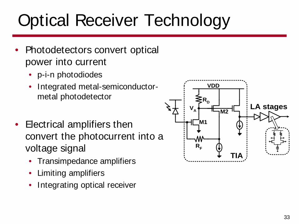
Optical Receiver Technology
• Photodetectors convert optical power into current• p-i-n photodiodes• Integrated metal-semiconductor-
metal photodetector
• Electrical amplifiers then convert the photocurrent into a voltage signal• Transimpedance amplifiers• Limiting amplifiers• Integrating optical receiver
RF
M1
M2
RD
VDD
VA
TIA
LA stages
33

p-i-n Photodiode
• Normally incident light absorbed in intrinsic region and generates carriers
• Trade-off between capacitance and transit-time
• Typical capacitance between 100-300fF
( ) ( )mA/mW108 5 ληλη
ρ pdpd
opt hcq
PI
×===
Wpd e αη −−=1
Wvf sat
trdBPD
45.02
4.23 ==
πτ
Responsivity:
Quantum Efficiency:
Transit-Time Limited Bandwidth:
[Sackinger]
34

Integrated Ge MSM Photodetector
SiO2
Cu
Ge
SiO2Silicon nitride
0.75 um
XSEM
Active area: < 2 um2Very low capacitance: <1 fF
Cu
SiN waveguide
2 um
Cu Cu
Ge
Detector
• Lateral Metal-Semiconductor-Metal (MSM Detector)• Silicon Nitride Waveguide-Coupled • Direct Germanium deposition on oxideI. Young, E. Mohammed, J. Liao, A. Kern, S. Palermo, B. Block, M. Reshotko, and P. Chang, “Optical I/O Technology for Tera-Scale Computing," IEEE Journal of Solid-State Circuits, 2010. 35

Agenda
• Electrical Channel Issues• Optical Channel• Optical Transmitter Technology• Optical Receiver Technology• Optical Integration Approaches
36

Optical Integration Approaches
• Efficient cost-effective optical integration approaches are necessary for optical interconnects to realize their potential for improved power efficiency at higher data rates
• Hybrid integration• Optical devices fabricated on a separate substrate
• Integrated CMOS photonics• Optical devices part of CMOS chip
37

Hybrid Integration
Wirebonding Flip-Chip Bonding
Short In-Package Traces
[Kromer] [Schow] [Mohammed]
38
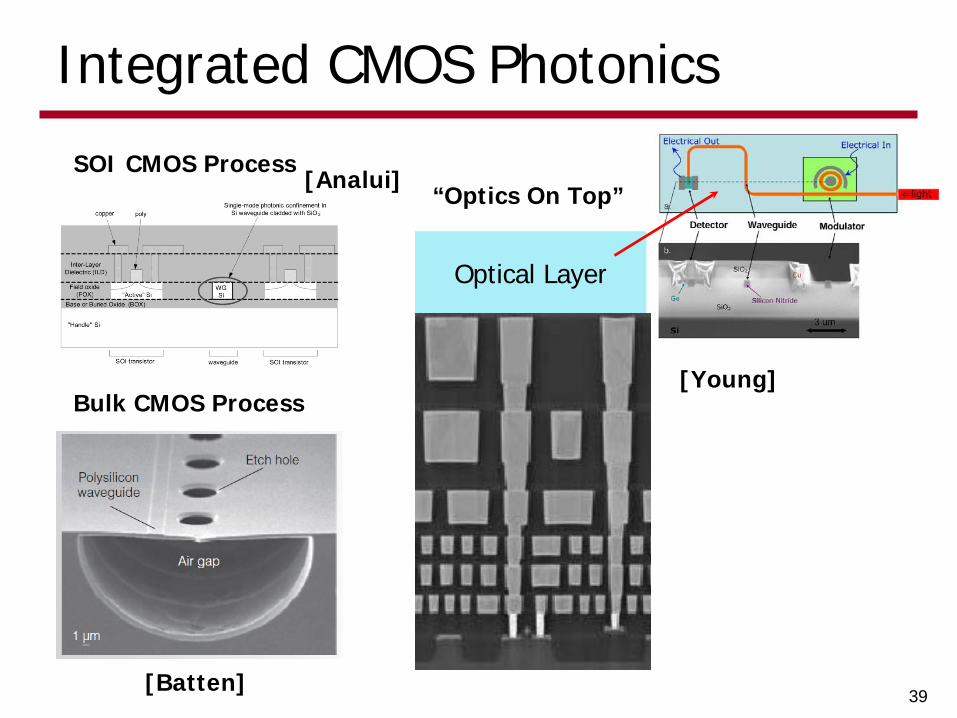
Integrated CMOS Photonics
Optical Layer
SOI CMOS Process
Bulk CMOS Process
“Optics On Top”[Analui]
[Batten]
[Young]
39

Future Photonic CMOS Chip
• Unified optical interconnect for on-chip core-to-core and off-chip processor-to-processor and processor-to-memory
I. Young, E. Mohammed, J. Liao, A. Kern, S. Palermo, B. Block, M. Reshotko, and P. Chang, “Optical I/O Technology for Tera-Scale Computing," IEEE International Solid-State Circuits Conference, 2009. 40

Conclusion
• Thanks for the fun semester!
41