ece606: solid state devices lecture 20 ...ee606/downloads/ece606_f...ece606: solid state devices...
TRANSCRIPT

Klimeck – ECE606 Fall 2012 – notes adopted from Alam
ECE606: Solid State DevicesLecture 20
Heterojunction Bipolar Transistor
Gerhard [email protected]
1
Klimeck – ECE606 Fall 2012 – notes adopted from Alam
Outline
2
1. Introduction2. Equilibrium solution for heterojunction3. Types of heterojunctions4. Intermediate Summary5. Abrupt junction HBTs6. Graded junction HBTs7. Graded base HBTs8. Double heterojunction HBTs9. Conclusions
“Heterostructure Fundamentals,” by Mark Lundstrom, Purdue University, 1995.
Herbert Kroemer, “Heterostructure bipolar transistors and integrated circuits,” Proc. IEEE , 70, pp. 13-25, 1982.

Klimeck – ECE606 Fall 2012 – notes adopted from Alam
How to make a better Transistor
3
( ),
,
,
,
2,
, ,
,
2
,
,g B
gg E
g E
BC B V B
C
EEi B
EE Vi E E
EN N ee
N Nn
n
e
ββ
β
−−
−= ≈
Heterojunction bipolar transistor
Graded Base transport
Polysilicon Emitter
Emitter bandgap > Base Bandgap
2,
, 2,
i B
i
E thpoly ballis ic
sEt
B
Nn
Nn
υβυ
→ × ×
Klimeck – ECE606 Fall 2012 – notes adopted from Alam
Heterojunction Bipolar Transistors
4
nemitter
ncollector n+
EG1>EG2
p+base
EG2 EG2
i) Wide gap Emitter HBT
ii) Double Heterojunction Bipolar Transistor
nemitter
ncollector n+
EG1>EG2
p+base
EG2 EG3>EG2

Klimeck – ECE606 Fall 2012 – notes adopted from Alam
Mesa HBTs
5
nemitter
ncollector n+
EG1>EG2
p+base
EG2 EG3>EG2
p+ basen-collector
n+
semi-insulating substrate
nMesa HBT
Intentional traps, Fermi level pinnedLow conductanceLow capacitanceHigh speed
Klimeck – ECE606 Fall 2012 – notes adopted from Alam
Applications
6
1) Optical fiber communications-40Gb/s…….160Gb/s
2) Wideband, high-resolution DA/AD convertersand digital frequency synthesizers
-military radar and communications
3) Monolithic, millimeter-wave IC’s (MMIC’s)
-front ends for receivers and transmitters
future need for transistors with 1 THz power-gain cutoff freq.

Klimeck – ECE606 Fall 2012 – notes adopted from Alam
Background
7
A heterojunction bipolar transistor
Schokley realized that HBT is possible, but Kroemer really provided the foundation of the field and worked out the details.
Kroemer
Klimeck – ECE606 Fall 2012 – notes adopted from Alam
Outline
8
1. Introduction2. Equilibrium solution for heterojunction3. Types of heterojunctions4. Intermediate Summary5. Abrupt junction HBTs6. Graded junction HBTs7. Graded base HBTs8. Double heterojunction HBTs9. Conclusions
“Heterostructure Fundamentals,” by Mark Lundstrom, Purdue University, 1995.
Herbert Kroemer, “Heterostructure bipolar transistors and integrated circuits,” Proc. IEEE , 70, pp. 13-25, 1982.

Klimeck – ECE606 Fall 2012 – notes adopted from Alam
Topic Map
9
Equi libr ium DC Small signal
Large Signal
Circuits
Diode
Schottky
BJT/HBT
MOS
Klimeck – ECE606 Fall 2012 – notes adopted from Alam
Bandgaps and Lattice Matching
10

Klimeck – ECE606 Fall 2012 – notes adopted from Alam
Band Diagram at Equilibrium
11
1P P P
pr g
t q
∂ = ∇ • − +∂
J
( )D AD q p n N N+ −∇ • = − + −
P P Pqp E qD pµ= − ∇J
1N N N
nr g
t q
∂ = ∇ • − +∂
J
J µ= + ∇N N Nqn E qD n
Equilibrium
DC dn/dt=0Small signal dn/dt ~ jωtn
Transient --- Charge control model
Klimeck – ECE606 Fall 2012 – notes adopted from Alam
N-Al0.3Ga0.7As: p-GaAs(Type-I Heterojunction)
12
Abrupt junction HBT
Vacuum Level
EC
EV
EF
χ2
χ1
EG≈ 1.80 eV
EG≈ 1.42 eV
ND NA
Klimeck – ECE606 Fall 2012 – notes adopted from Alam
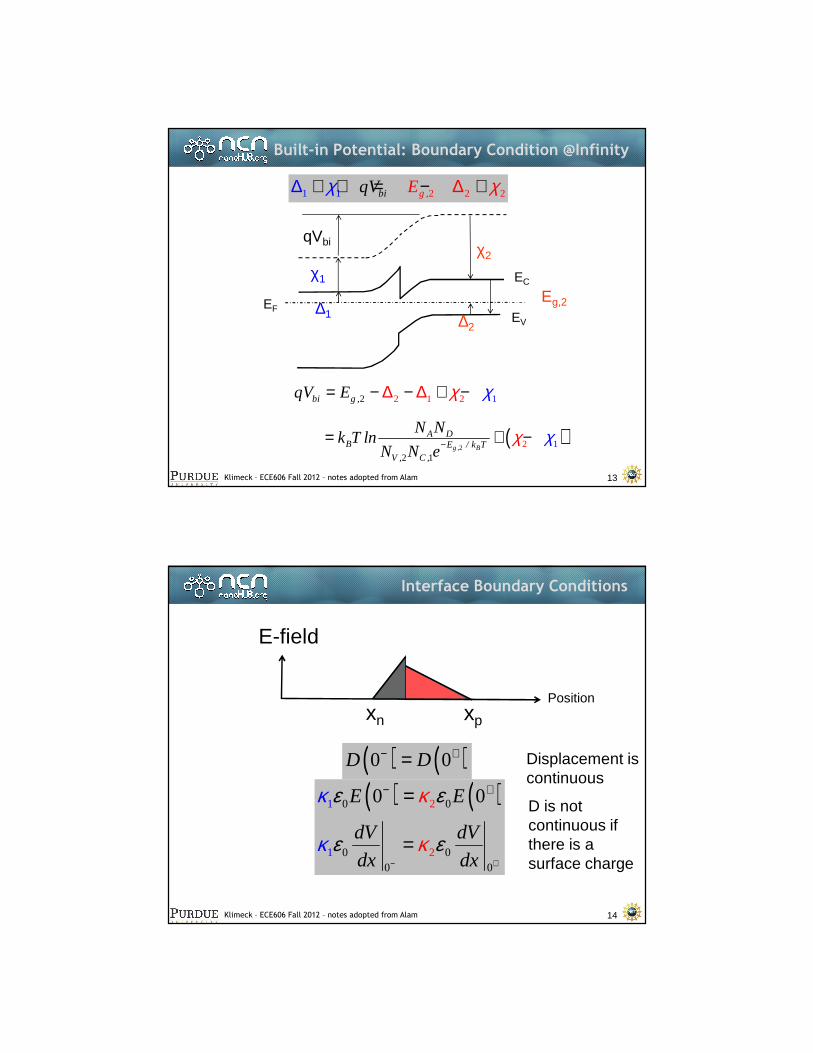
Built-in Potential: Boundary Condition @Infinity
13
qVbi
∆1 ∆2
Eg,2
EC
EV
EF
χ2
χ1
21 2 21 gi ,bqV E+ + = − ∆∆ + χχ
2 2 1 2 1bi g ,qV E ∆ ∆= − − + −χ χ
( )2
2 1
12g , B
A DB E / k T
V , C ,
N Nk T ln
N N e−= + −χ χ
Klimeck – ECE606 Fall 2012 – notes adopted from Alam
Interface Boundary Conditions
14
( ) ( )0 0D D− +=
Position
E-field
xn xp
( ) ( )0 0
0
2
2
1
00
10
0 0E E
dV dV
dx dx
κ
κ
ε
ε
κ
κ
ε
ε− +
− +=
=
D is not continuous if there is a surface charge
Displacement is continuous
Klimeck – ECE606 Fall 2012 – notes adopted from Alam
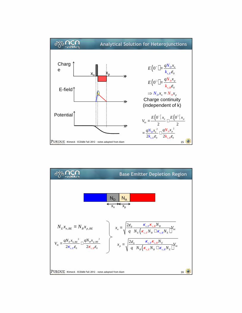
Analytical Solution for Heterojunctions
15
Charge
xpxn x
Potential
x
E-field
x
( ) ( )2
,
2
0,0
0 0
2 2
2 2
n p
bi
pn
s B
D A
E s
E x E xV
q xq N
kk
xN
ε ε
− +
= +
= +
( )
( ), 0
, 0
0
0 A
s B
D
s E
D
n
n A
p
p
N
q xE
q xE
x x
N
k
k
NN
ε
ε
−
+
=
=
⇒ =Charge continuity (independent of k)
Klimeck – ECE606 Fall 2012 – notes adopted from Alam
Base Emitter Depletion Region
16
ND NA
,
22,,
0 0,2 2s E
B p BEE n BEbi
s B
qN xqN xV
ε κ εκ= +
, ,E n BE B p BEN x N x=( )
,
,,
0 ,2 s BBn bi
E B
s E
sE EBs
Nx V
q N N N
εκ κ
κκ=
+
xn
( ),
,,
0 ,2 s EBp bi
B B
s E
sE EBs
Nx V
q N N N
εκ κ
κκ=
+
xp
Klimeck – ECE606 Fall 2012 – notes adopted from Alam
Outline
17
1. Introduction2. Equilibrium solution for heterojunction3. Types of heterojunctions4. Intermediate Summary5. Abrupt junction HBTs6. Graded junction HBTs7. Graded base HBTs8. Double heterojunction HBTs9. Conclusions
“Heterostructure Fundamentals,” by Mark Lundstrom, Purdue University, 1995.
Herbert Kroemer, “Heterostructure bipolar transistors and integrated circuits,” Proc. IEEE , 70, pp. 13-25, 1982.
Klimeck – ECE606 Fall 2012 – notes adopted from Alam
N-Al0.3Ga0.7As: p-GaAs(Type-I Heterojunction)
18
Abrupt junction HBT
Vacuum Level
EC
EV
EF
χ2
χ1
EG≈ 1.80 eV
EG≈ 1.42 eV
ND NA

Klimeck – ECE606 Fall 2012 – notes adopted from Alam
P-Al0.3Ga0.7As : n-GaAs (Type I junctions)
Alam ECE-606 S09 19
E0Vacuum level
χ1
EC
EV
EC
EV
EG≈ 1.80 eV
EG≈ 1.42 eV
χ2
V
jP
V
jn
∆EV
qV (x)
El
qVBI
∆EC
EF
Depletion layerDepletion layer
Klimeck – ECE606 Fall 2012 – notes adopted from Alam
N-p vs P-n of Type I Heterostructure
20
Klimeck – ECE606 Fall 2012 – notes adopted from Alam
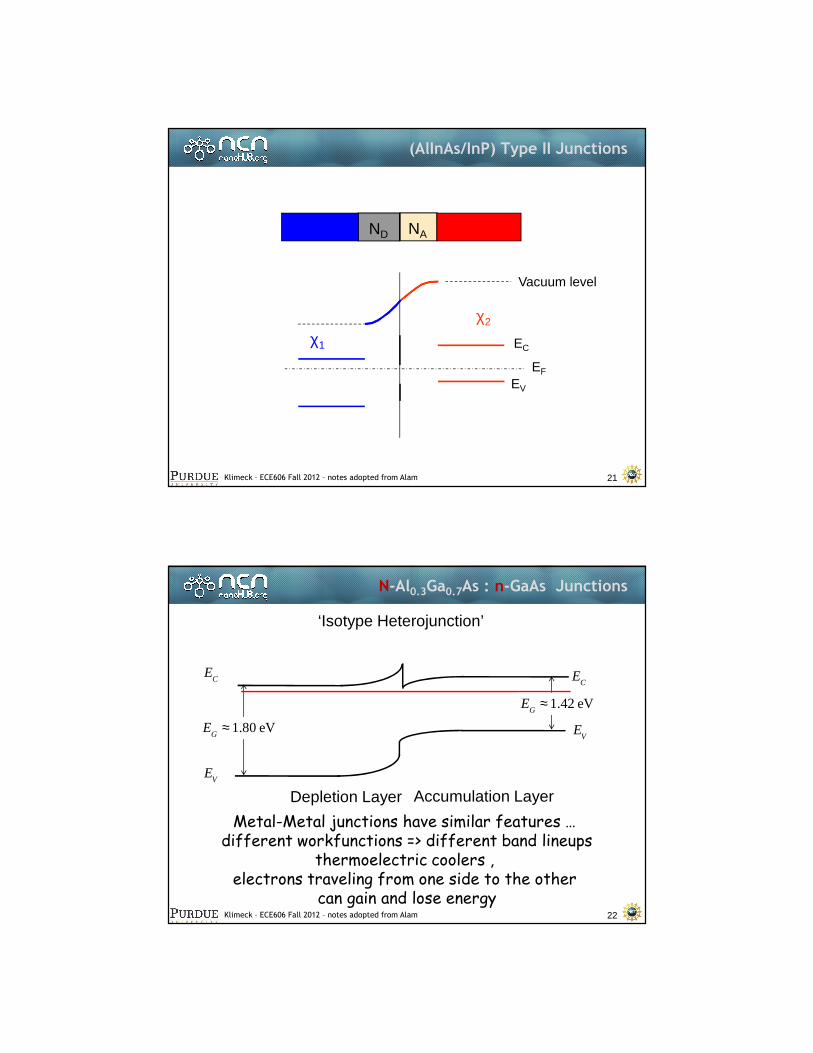
(AlInAs/InP) Type II Junctions
21
ND NA
Vacuum level
EC
EV
EF
χ2
χ1
Klimeck – ECE606 Fall 2012 – notes adopted from Alam
N-Al0.3Ga0.7As : n-GaAs Junctions
22
EC
EV
EC
EV
EG≈ 1.80 eV
EG≈ 1.42 eV
‘Isotype Heterojunction’
EV
Accumulation LayerDepletion Layer
Metal-Metal junctions have similar features … different workfunctions => different band lineups
thermoelectric coolers , electrons traveling from one side to the other
can gain and lose energy

Klimeck – ECE606 Fall 2012 – notes adopted from Alam
P-GaSb : n-InAs (Type III)
23
EC
EV
EC
EV
E0 Field-free vacuum level
χ1
χ2
EFP
EG≈ 0.72 eV
EFn
EG≈ 0.36 eV
Klimeck – ECE606 Fall 2012 – notes adopted from Alam
P-GaSb : n-InAs (Type III)
24
EC
EV
EC
EV
∆EC
= 0.87 eV
EF EG
≈ 0.72 eV
EG≈ 0.36 eV
Accumulation Layer!Accumulation Layer!

Klimeck – ECE606 Fall 2012 – notes adopted from Alam
Conclusion
25
1. Heterojunction transistors offer a solution to the limitations of poly-Si bipolar transistors.
2. Equilibrium solutions for HBTs are very similar to those of normal BJTs.
3. Depending on the alignment, there could be different types of heterojuctions. Each has different usage.
4. We will discuss current transport in HBTs in the next section.
Klimeck – ECE606 Fall 2012 – notes adopted from Alam
Outline
26
1. Introduction2. Equilibrium solution for heterojunction3. Types of heterojunctions4. Intermediate Summary5. Abrupt junction HBTs6. Graded junction HBTs7. Graded base HBTs8. Double heterojunction HBTs9. Conclusions
“Heterostructure Fundamentals,” by Mark Lundstrom, Purdue University, 1995.
Herbert Kroemer, “Heterostructure bipolar transistors and integrated circuits,” Proc. IEEE , 70, pp. 13-25, 1982.
Klimeck – ECE606 Fall 2012 – notes adopted from Alam
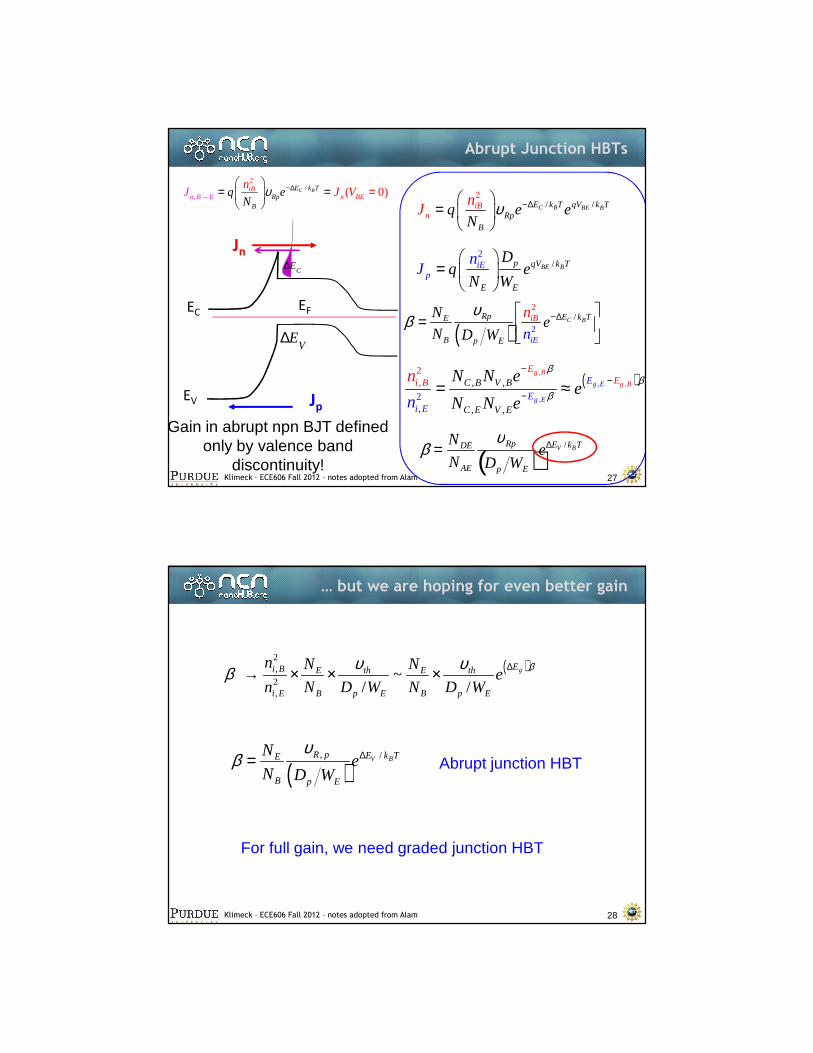
Abrupt Junction HBTs
27
EC EF
EV
Jn
Jp
/2
BE Bp qV k
E E
iEp
TnJ
Dq e
N W
=
( )2
2/C B
i
Rp E k TE
B p E
iB
E
Ne
n
n
N D W
υβ −∆
=
2/ /C B BE BE k T qV k T
RpnB
iBqJN
ne eυ −∆
=
β =NDE
NAE
υRp
Dp WE( )e∆EV /kBT
∆EV
Gain in abrupt npn BJT defined only by valence band
discontinuity!
2/
, ( 0)C BE k TR
iBnn B E BEp
B
q eN
nJJ Vυ −∆
→
= =
=
∆EC
( ),
,
,
,
2,
, ,
,
2
,
,g B
gg E
g E
BC B V B
C
EEi B
EE Vi E E
EN N ee
N Nn
n
e
ββ
β
−−
−= ≈
Klimeck – ECE606 Fall 2012 – notes adopted from Alam
… but we are hoping for even better gain
28
( )2,
2,
~/ /
gEi B E th E th
i E B p E B p E
n N Ne
n N D W N D W
∆→ × × × βυ υβ
( ), /V BR p E k TE
B p E
Ne
N D W∆=
υβ Abrupt junction HBT
For full gain, we need graded junction HBT
Klimeck – ECE606 Fall 2012 – notes adopted from Alam
Outline
29
1. Introduction2. Equilibrium solution for heterojunction3. Types of heterojunctions4. Intermediate Summary5. Abrupt junction HBTs6. Graded junction HBTs7. Graded base HBTs8. Double heterojunction HBTs9. Conclusions
“Heterostructure Fundamentals,” by Mark Lundstrom, Purdue University, 1995.
Herbert Kroemer, “Heterostructure bipolar transistors and integrated circuits,” Proc. IEEE , 70, pp. 13-25, 1982.
Klimeck – ECE606 Fall 2012 – notes adopted from Alam
Abrupt Junction
30
EC
EC
EV
EG≈ 1.80 eV
V
jN V
jp
∆EV
EG≈ 1.42 eV
EV
V (x)
x xP −x
N
χ(x)
x xP −x
N E
C(x) = E
0− χ(x)−qV x( )
EV(x) = E
C(x)− E
G(x)

Klimeck – ECE606 Fall 2012 – notes adopted from Alam
Graded Base-Emitter Junction
31
EC
EC
EV
EG≈ 1.80 eV ∆E
V
EG≈ 1.42 eV
EV
V (x)
x xP −x
N
χ(x)
x xP −x
N E
C(x) = E
0− χ(x)−qV x( )
EV(x) = E
C(x)− E
G(x)
Klimeck – ECE606 Fall 2012 – notes adopted from Alam
Current Gain
32
EC
EF
EV
x
Jn
Jp
2/BE Bp qV k Ti
Dp
E
E E
Dn
N WJ q e
=
EGE > EGB
β =NDE
NAE
Dn
Dp
WE
WB
niB2
niE2
ni = NCNV e−EG /2kBT
β ≈NDE
NAE
Dn
Dp
WE
WB
e∆EG /kBT
2/BE BqV kn
ABn
TiB
B
n D
N WJ q e
=
No exponential Suppression!

Klimeck – ECE606 Fall 2012 – notes adopted from Alam
Advantages of HBT: Inverted Base Doping
33
/G BE k TDE n EDC
AB p B
N D We
N D Wβ ∆≈
1) Thin Base for high speed
2) Very heavily doped Base to prevent Punch Through,reduce Early effect, and to lower Rex
3) Moderately doped Emitter (lower Cj,BE)
“inverted base doping” NAB >> NDE
Klimeck – ECE606 Fall 2012 – notes adopted from Alam
Outline
34
1. Introduction2. Equilibrium solution for heterojunction3. Types of heterojunctions4. Intermediate Summary5. Abrupt junction HBTs6. Graded junction HBTs7. Graded base HBTs8. Double heterojunction HBTs9. Conclusions
“Heterostructure Fundamentals,” by Mark Lundstrom, Purdue University, 1995.
Herbert Kroemer, “Heterostructure bipolar transistors and integrated circuits,” Proc. IEEE , 70, pp. 13-25, 1982.
Klimeck – ECE606 Fall 2012 – notes adopted from Alam
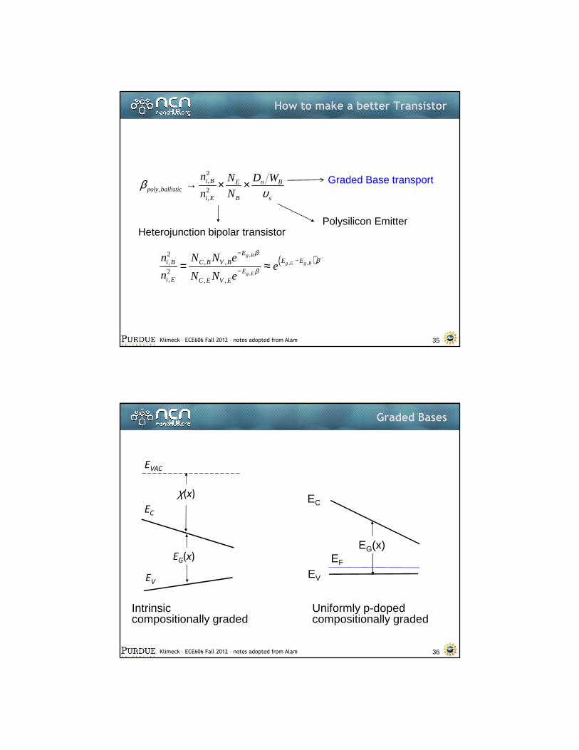
How to make a better Transistor
35
( ),
, ,
,
2, , ,
2, , ,
g B
g E g B
g E
EE Ei B C B V B
Ei E C E V E
n N N ee
n N N e
−−
−= ≈β
ββ
Heterojunction bipolar transistor
Graded Base transport
Polysilicon Emitter
2,
, 2,
i B E n Bpoly ballistic
i E B s
n N D W
n Nβ
υ→ × ×
Klimeck – ECE606 Fall 2012 – notes adopted from Alam
Graded Bases
36
EC
EV
χ(x)
EVAC
EG(x)
Intrinsiccompositionally graded
EC
EV
EG(x)EF
Uniformly p-dopedcompositionally graded

Klimeck – ECE606 Fall 2012 – notes adopted from Alam
Graded Base HBTs
37
EC
EV
x
Jp
EF2
/BE Bp qV k TiE
E EpJ
Dnq e
N W
=
2
2E n E
DCB
i
p B iE
BN D W n
N D W nβ =
2
2eff
B Bb
n n
W W
Dτ
µ= <<
E
Geff
B
E q
W
∆=E
Jn2
/BE BqV k Tn
Bn
B
B
iJD
q eW
n
N
=
Klimeck – ECE606 Fall 2012 – notes adopted from Alam
Outline
38
1. Introduction2. Equilibrium solution for heterojunction3. Types of heterojunctions4. Intermediate Summary5. Abrupt junction HBTs6. Graded junction HBTs7. Graded base HBTs8. Double heterojunction HBTs9. Conclusions
“Heterostructure Fundamentals,” by Mark Lundstrom, Purdue University, 1995.
Herbert Kroemer, “Heterostructure bipolar transistors and integrated circuits,” Proc. IEEE , 70, pp. 13-25, 1982.

Klimeck – ECE606 Fall 2012 – notes adopted from Alam
Double HBJT
39
EC
EF
EV
x
Jn
Jp
EGE > EGBEGC > EGE
• Symmetrical operation(simplify circuiots)
• No charge storage whenthe b-c junction is forwardbiased(ni is smaller)
• Reduced collector offsetvoltage
• Higher collectorbreakdown voltage(higher gap)
Klimeck – ECE606 Fall 2012 – notes adopted from Alam
Offset Voltage
40
IC
IB
VCE
does I C = 0 at VCE = 0?
C
E
B ICVB
I B

Klimeck – ECE606 Fall 2012 – notes adopted from Alam
Offset Voltage
41
EC
EF
EV
x
J1( )
2
1/B E Bq V V k TiB n
AB B
Jn D
q eN W
− =
J2
( )2
2/B C Bq V V k TiB n
AB B
Jn D
q eN W
− =
J3
( )2
3/B C Bq V V k TpiC
DC C
JDn
q eN W
− =
1 2 3C J JJ J= − −
set JC = 0, assume VE = 0, solve for VC=VOS
Klimeck – ECE606 Fall 2012 – notes adopted from Alam
Offset Voltage Result
42
VOS =kBT
qln 1+ 1 γ R( )
( )( )( )( )
2
2
23
iB AB n B
R
iC DC p C
n N D
J
W
n N W
J
Dγ = = (Reverse Emitter injection efficiency)
Want a large γR for small Vos. Wide bandgap collector helps.

Klimeck – ECE606 Fall 2012 – notes adopted from Alam
Outline
43
1. Introduction2. Equilibrium solution for heterojunction3. Types of heterojunctions4. Intermediate Summary5. Abrupt junction HBTs6. Graded junction HBTs7. Graded base HBTs8. Double heterojunction HBTs9. Conclusions – modern design
“Heterostructure Fundamentals,” by Mark Lundstrom, Purdue University, 1995.
Herbert Kroemer, “Heterostructure bipolar transistors and integrated circuits,” Proc. IEEE , 70, pp. 13-25, 1982.
Klimeck – ECE606 Fall 2012 – notes adopted from Alam
Putting the Terms Together
44
2
, ,
1
2 2 2B BC
T n sat
Bj BC j BE
C
W W
f D
k TC C
qI
= + +
+
π υ
10log Tf
10log CI
Kirk Current
Quations: Why does HBTs have such high performance ?
KI
Base transit time
Collector transit time
junction charging time …
Klimeck – ECE606 Fall 2012 – notes adopted from Alam
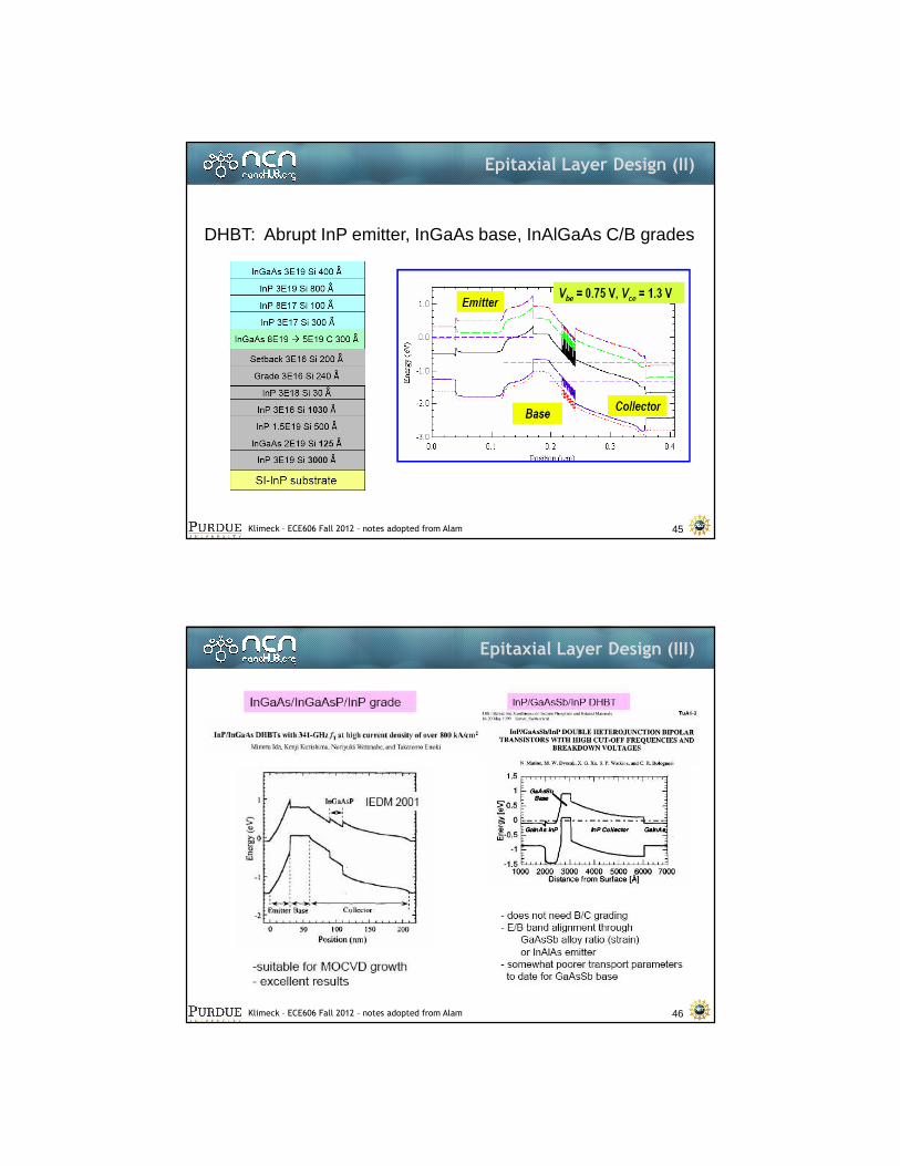
Epitaxial Layer Design (II)
45
DHBT: Abrupt InP emitter, InGaAs base, InAlGaAs C/B grades
Klimeck – ECE606 Fall 2012 – notes adopted from Alam
Epitaxial Layer Design (III)
46
Klimeck – ECE606 Fall 2012 – notes adopted from Alam
Summary
47
1) The use of a wide bandgap emitter has two benefits:-allows heavy base doping-allows moderate emitter doping
2) The use of a wide bandgap collector has benefits:
-symmetrical device-reduced charge storage in saturation-reduced collector offset voltage-higher collector breakdown voltage
3) Bandgap engineering has potential benefits:
-heterojunction launching ramps-compositionally graded bases-elimination of band spikes
4) HBTs have the potential for THz cutoff frequencies. However, it has yield issues and heating and contact R problems.
Klimeck – ECE606 Fall 2012 – notes adopted from Alam
Outline from previous lecture
48
1) Current gain in BJTs
2) Considerations for base doping
3) Considerations for collector doping
4) Intermediate Summary
5) Problems of classical transistor
6) Poly-Si emitter
7) Short base transport
8) High frequency response
9) Conclusions
REF: SDF, Chapter 10

Klimeck – ECE606 Fall 2012 – notes adopted from Alam
Topic Map
49
Equilibrium DC Small signal
Large Signal
Circuits
Diode
Schottky
BJT/HBT
MOS
Klimeck – ECE606 Fall 2012 – notes adopted from Alam
Small Signal Response
50
P+
N
P
C
E E
B
VEB(in)
VEC(out)
ICIB
log10 β
log10 f
fT
1
fβ
2
, ,
1
2 2 2B BC B
j BC j BET n sat C
W W k TC C
f D qI
= + + +
π υ
β ω( ) ≈ βDC
ωβ
ω
Desire high fT⇒High IC⇒Low capacitances⇒Low widths

Klimeck – ECE606 Fall 2012 – notes adopted from Alam
Frequency Response
51
� The gain of an amplifier is affected by the capacitance associated with its circuit.� This capacitance reduces the gain in both the low and high frequency ranges of
operation.� The reduction of gain in the low frequency band is due to the coupling
and bypass capacitors selected. They are essentially short circuits in themid and high bands.
� The reduction of gain in the high frequency band is due to the internalcapacitance of the amplifying device, e.g., BJT, FET, etc.
� This capacitance is represented by capacitors in the small signal equivalent circuit for these devices. They are essentially open circuits in the low and mid bands.
Klimeck – ECE606 Fall 2012 – notes adopted from Alam
Small Signal Response (Common Emitter)From Ebers Moll Model
52
Cµ
( )1 F FIα−
Cπ
IRF F R RI Iα α−
( )/0 1BEqV kT
F FI I e= −
( )11 F F
BE
B B
BE B
Idd q
r dV dV T
I
k
I
π
α =−
= =
( )F C
BE Bm
Fd qI
dV Tg
I
k
α= =
( )F F B BEmm Eg VI gδ δα υ= =
P+
N
P
C
E E
B
VEB(in)
VEC(out)
ICIB
IB
1 C
DC B
qI
k Tβ=
DC Circuit => AC small signal CircuitBC In reverse bias, IR=0
Cµ
Cπrππππ gmVBE
IBIC
IE

Klimeck – ECE606 Fall 2012 – notes adopted from Alam
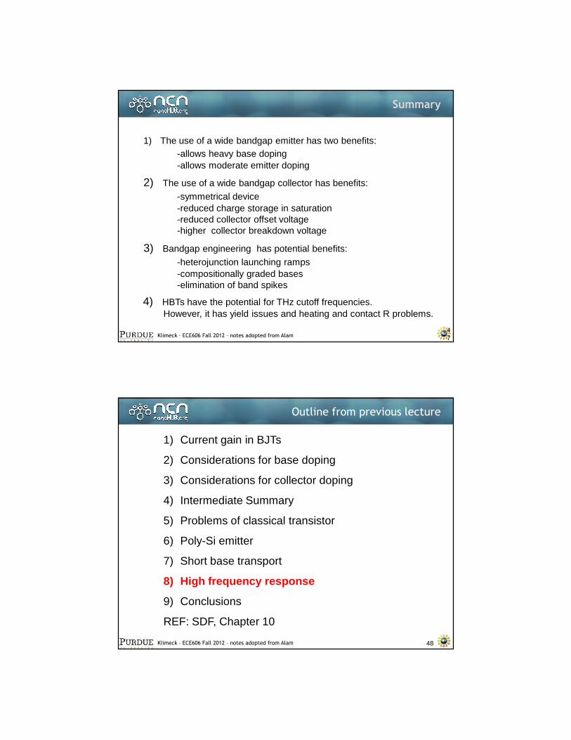
Short Circuit Current Gain
53
( )( )1
1T
T mT
T
m j gf
j C Cj C j
g
Cr
C
π µπ µ
π
µωβ
ω ω ω−
≡ = ≈ +
+ +
( )1
m BE CB
BE BE BCB
Cj
f
j C j
C
Ci
r
gi
π µπ
µω υβ
υ ω υ ω
υ
υ
+= =
+ +
Cπrπ
m BEg υ
Cµ
( ) ( ), , , ,
1 1
2 j BC jT
BBE d B
B
m C CC d BE
T
C k T k T
g
CC C C C
f qI qIπ µ
πω+
≡ = = + + +
,,
d BCB Bd BC
C C BE C
Ck T dQC
qI dI dV dI= =
E
CB
Klimeck – ECE606 Fall 2012 – notes adopted from Alam
Short Circuit Current Gain
54
( )( )1
1T
T mT
T
m j gf
j C Cj C j
g
Cr
C
π µπ µ
π
µωβ
ω ω ω−
≡ = ≈ +
+ +
Cπrπ
m BEg υ
Cµ
( ) ( ), , , ,
1 1
2 j BC j
T
BBE d B
B
m C C
C d BE
T
C k T k T
g
CC C C C
f qI qIπ µ
πω+
≡ = = + + +
,,
d BCB Bd BC
C C BE C
Ck T dQC
qI dI dV dI= =
E
CB
Klimeck – ECE606 Fall 2012 – notes adopted from Alam
Short Circuit Current Gain
55
Cπrπ
m BEg υ
Cµ
( ) ( ), , , ,
1 1
2 j BC j
T
BBE d B
B
m C C
C d BE
T
C k T k T
g
CC C C C
f qI qIπ µ
πω+
≡ = = + + +
,,
d BCB Bd BC
C C BE C
Ck T dQC
qI dI dV dI= =
E
CB
Klimeck – ECE606 Fall 2012 – notes adopted from Alam
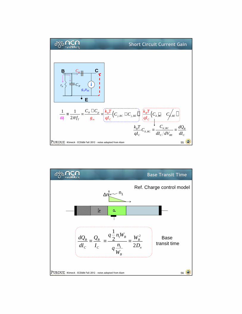
Base Transit Time
56
B B
C C
dQ Q
dI I=
N+ P
∆n n1
21
1
12
2
BB
n
B
q nW Wn Dq
W
= =
Ref. Charge control model
Base transit time

Klimeck – ECE606 Fall 2012 – notes adopted from Alam
Collector Transit Time
57
?BC
sat
W=τυ
N+ P
1
2qi τ× × =
, 2 2BC
eff BCsat
q W
i
ττυ
= = =
t
i τ
Electrons injected into collector depletion region – very high fields more than diffusion => drift => acceleration of carriersCharge imaged in collector
Klimeck – ECE606 Fall 2012 – notes adopted from Alam
Putting the Terms Together
58
2
, ,
1
2 2 2B BC
T n sat
Bj BC j BE
C
W W
f D
k TC C
qI
= + +
+
π υ
Base transit time
Collector transit time
Junction charging time
10log Tf
10log CI
Kirk Current
Do you see the motivation to reduce WB and WBC as much as possible? What problem would you face if you push this too far ?
KI
Increasing IC too high reduces WBC and increases the overall capacitance=> frequency rolls off….

Klimeck – ECE606 Fall 2012 – notes adopted from Alam
High Frequency Metrics
59
( ) ( )2
, ,
1
2 2 2B BC B
j BE j BCT n sat C
ex c cb
W W k T qC C R
f DR C
Iτ
π υ= = + + ++ +
(current-gain cutoff frequency, fT)
(power-gain cutoff frequency, fmax)
fmax =fT
8π RbbCcbi
Klimeck – ECE606 Fall 2012 – notes adopted from Alam
Summary
60
We have discussed various modifications of the classical
BJTs and explained why improvement of performance
has become so difficult in recent years.
The small signal analysis illustrates the importance of
reduced junction capacitance, resistances, and transit
times.
Classical homojunctions BJTs can only go so far, further
improvement is possible with heterojunction bipolar
transistors.